JP6331997B2 - Semiconductor optical device - Google Patents
Semiconductor optical device Download PDFInfo
- Publication number
- JP6331997B2 JP6331997B2 JP2014241903A JP2014241903A JP6331997B2 JP 6331997 B2 JP6331997 B2 JP 6331997B2 JP 2014241903 A JP2014241903 A JP 2014241903A JP 2014241903 A JP2014241903 A JP 2014241903A JP 6331997 B2 JP6331997 B2 JP 6331997B2
- Authority
- JP
- Japan
- Prior art keywords
- refractive index
- diffraction grating
- layer
- optical device
- semiconductor optical
- Prior art date
- Legal status (The legal status is an assumption and is not a legal conclusion. Google has not performed a legal analysis and makes no representation as to the accuracy of the status listed.)
- Active
Links
- 230000003287 optical effect Effects 0.000 title claims description 64
- 239000004065 semiconductor Substances 0.000 title claims description 62
- 239000000758 substrate Substances 0.000 claims description 15
- 230000007423 decrease Effects 0.000 claims description 9
- 230000000737 periodic effect Effects 0.000 description 19
- 230000008878 coupling Effects 0.000 description 18
- 238000010168 coupling process Methods 0.000 description 18
- 238000005859 coupling reaction Methods 0.000 description 18
- 239000000463 material Substances 0.000 description 16
- 238000004519 manufacturing process Methods 0.000 description 9
- 230000004048 modification Effects 0.000 description 9
- 238000012986 modification Methods 0.000 description 9
- 238000005530 etching Methods 0.000 description 7
- 230000000052 comparative effect Effects 0.000 description 5
- 230000008901 benefit Effects 0.000 description 3
- 238000005253 cladding Methods 0.000 description 3
- 230000000694 effects Effects 0.000 description 3
- 229910004298 SiO 2 Inorganic materials 0.000 description 2
- 230000008859 change Effects 0.000 description 2
- 239000002019 doping agent Substances 0.000 description 2
- 238000000034 method Methods 0.000 description 2
- 229910000530 Gallium indium arsenide Inorganic materials 0.000 description 1
- 230000003247 decreasing effect Effects 0.000 description 1
- 230000006866 deterioration Effects 0.000 description 1
- 238000010586 diagram Methods 0.000 description 1
- 239000003989 dielectric material Substances 0.000 description 1
- 239000006185 dispersion Substances 0.000 description 1
- 238000009826 distribution Methods 0.000 description 1
- 235000012489 doughnuts Nutrition 0.000 description 1
- 230000031700 light absorption Effects 0.000 description 1
- 239000000203 mixture Substances 0.000 description 1
- 239000004038 photonic crystal Substances 0.000 description 1
- 229920000642 polymer Polymers 0.000 description 1
Images


Classifications
-
- H—ELECTRICITY
- H01—ELECTRIC ELEMENTS
- H01S—DEVICES USING THE PROCESS OF LIGHT AMPLIFICATION BY STIMULATED EMISSION OF RADIATION [LASER] TO AMPLIFY OR GENERATE LIGHT; DEVICES USING STIMULATED EMISSION OF ELECTROMAGNETIC RADIATION IN WAVE RANGES OTHER THAN OPTICAL
- H01S5/00—Semiconductor lasers
- H01S5/10—Construction or shape of the optical resonator, e.g. extended or external cavity, coupled cavities, bent-guide, varying width, thickness or composition of the active region
- H01S5/12—Construction or shape of the optical resonator, e.g. extended or external cavity, coupled cavities, bent-guide, varying width, thickness or composition of the active region the resonator having a periodic structure, e.g. in distributed feedback [DFB] lasers
-
- H—ELECTRICITY
- H01—ELECTRIC ELEMENTS
- H01S—DEVICES USING THE PROCESS OF LIGHT AMPLIFICATION BY STIMULATED EMISSION OF RADIATION [LASER] TO AMPLIFY OR GENERATE LIGHT; DEVICES USING STIMULATED EMISSION OF ELECTROMAGNETIC RADIATION IN WAVE RANGES OTHER THAN OPTICAL
- H01S3/00—Lasers, i.e. devices using stimulated emission of electromagnetic radiation in the infrared, visible or ultraviolet wave range
- H01S3/05—Construction or shape of optical resonators; Accommodation of active medium therein; Shape of active medium
- H01S3/06—Construction or shape of active medium
- H01S3/063—Waveguide lasers, i.e. whereby the dimensions of the waveguide are of the order of the light wavelength
- H01S3/067—Fibre lasers
- H01S3/0675—Resonators including a grating structure, e.g. distributed Bragg reflectors [DBR] or distributed feedback [DFB] fibre lasers
-
- H—ELECTRICITY
- H01—ELECTRIC ELEMENTS
- H01S—DEVICES USING THE PROCESS OF LIGHT AMPLIFICATION BY STIMULATED EMISSION OF RADIATION [LASER] TO AMPLIFY OR GENERATE LIGHT; DEVICES USING STIMULATED EMISSION OF ELECTROMAGNETIC RADIATION IN WAVE RANGES OTHER THAN OPTICAL
- H01S3/00—Lasers, i.e. devices using stimulated emission of electromagnetic radiation in the infrared, visible or ultraviolet wave range
- H01S3/10—Controlling the intensity, frequency, phase, polarisation or direction of the emitted radiation, e.g. switching, gating, modulating or demodulating
- H01S3/105—Controlling the intensity, frequency, phase, polarisation or direction of the emitted radiation, e.g. switching, gating, modulating or demodulating by controlling the mutual position or the reflecting properties of the reflectors of the cavity, e.g. by controlling the cavity length
- H01S3/1055—Controlling the intensity, frequency, phase, polarisation or direction of the emitted radiation, e.g. switching, gating, modulating or demodulating by controlling the mutual position or the reflecting properties of the reflectors of the cavity, e.g. by controlling the cavity length one of the reflectors being constituted by a diffraction grating
-
- H—ELECTRICITY
- H01—ELECTRIC ELEMENTS
- H01S—DEVICES USING THE PROCESS OF LIGHT AMPLIFICATION BY STIMULATED EMISSION OF RADIATION [LASER] TO AMPLIFY OR GENERATE LIGHT; DEVICES USING STIMULATED EMISSION OF ELECTROMAGNETIC RADIATION IN WAVE RANGES OTHER THAN OPTICAL
- H01S5/00—Semiconductor lasers
- H01S5/10—Construction or shape of the optical resonator, e.g. extended or external cavity, coupled cavities, bent-guide, varying width, thickness or composition of the active region
- H01S5/12—Construction or shape of the optical resonator, e.g. extended or external cavity, coupled cavities, bent-guide, varying width, thickness or composition of the active region the resonator having a periodic structure, e.g. in distributed feedback [DFB] lasers
- H01S5/1231—Grating growth or overgrowth details
-
- H—ELECTRICITY
- H01—ELECTRIC ELEMENTS
- H01S—DEVICES USING THE PROCESS OF LIGHT AMPLIFICATION BY STIMULATED EMISSION OF RADIATION [LASER] TO AMPLIFY OR GENERATE LIGHT; DEVICES USING STIMULATED EMISSION OF ELECTROMAGNETIC RADIATION IN WAVE RANGES OTHER THAN OPTICAL
- H01S5/00—Semiconductor lasers
- H01S5/10—Construction or shape of the optical resonator, e.g. extended or external cavity, coupled cavities, bent-guide, varying width, thickness or composition of the active region
- H01S5/18—Surface-emitting [SE] lasers, e.g. having both horizontal and vertical cavities
- H01S5/183—Surface-emitting [SE] lasers, e.g. having both horizontal and vertical cavities having only vertical cavities, e.g. vertical cavity surface-emitting lasers [VCSEL]
- H01S5/18308—Surface-emitting [SE] lasers, e.g. having both horizontal and vertical cavities having only vertical cavities, e.g. vertical cavity surface-emitting lasers [VCSEL] having a special structure for lateral current or light confinement
- H01S5/18319—Surface-emitting [SE] lasers, e.g. having both horizontal and vertical cavities having only vertical cavities, e.g. vertical cavity surface-emitting lasers [VCSEL] having a special structure for lateral current or light confinement comprising a periodical structure in lateral directions
-
- H—ELECTRICITY
- H01—ELECTRIC ELEMENTS
- H01S—DEVICES USING THE PROCESS OF LIGHT AMPLIFICATION BY STIMULATED EMISSION OF RADIATION [LASER] TO AMPLIFY OR GENERATE LIGHT; DEVICES USING STIMULATED EMISSION OF ELECTROMAGNETIC RADIATION IN WAVE RANGES OTHER THAN OPTICAL
- H01S5/00—Semiconductor lasers
- H01S5/20—Structure or shape of the semiconductor body to guide the optical wave ; Confining structures perpendicular to the optical axis, e.g. index or gain guiding, stripe geometry, broad area lasers, gain tailoring, transverse or lateral reflectors, special cladding structures, MQW barrier reflection layers
Landscapes
- Physics & Mathematics (AREA)
- Electromagnetism (AREA)
- Optics & Photonics (AREA)
- Condensed Matter Physics & Semiconductors (AREA)
- General Physics & Mathematics (AREA)
- Engineering & Computer Science (AREA)
- Plasma & Fusion (AREA)
- Semiconductor Lasers (AREA)
Description
本発明は、半導体光素子に関する。 The present invention relates to a semiconductor light emitting element.
従来、例えば、下記の特許文献1、2に記載されているように、共振器内部に複素結合型の回折格子を備える分布帰還型レーザ素子(DFB−LD)が知られている。特許文献1によれば、屈折率結合型、利得結合型、および複素結合型のそれぞれのDFBレーザは次のように対比される。屈折率結合型DFBレーザは、共振器内部で複素屈折率の実部のみが周期的に変動しているタイプ、つまり周期的に屈折率を変化させる回折格子を共振器内に備えている半導体レーザ素子である。利得結合型DFBレーザは、共振器内部で複素屈折率の虚部のみが周期的に変動しているタイプ、つまり周期的に利得を変化させる、又は周期的に損失を変化させる回折格子を共振器内に備えている半導体レーザ素子である。複素結合型DFBレーザは、共振器内部で複素屈折率の実部及び虚部の双方が周期的に変動しているタイプの半導体レーザ素子である。
Conventionally, for example, as described in
利得結合型の回折格子は光吸収層を含むので、しきい値電流の上昇、スロープ効率の低下、および消費電力が大きいといった問題点がある。これに対し、屈折率結合型の回折格子を用いた場合にはこれらの問題を回避できるという利点がある。 Since the gain-coupled diffraction grating includes a light absorption layer, there are problems such as an increase in threshold current, a decrease in slope efficiency, and large power consumption. On the other hand, when a refractive index coupling type diffraction grating is used, there is an advantage that these problems can be avoided.
ところで、DFBレーザを製造する際には、エッチングにより回折格子を形成した後、さらに回折格子埋込層を成長し、この回折格子埋込層の上に光閉込層、活性層などが設けられる。このとき、製造ばらつきにより回折格子が設計値よりも深く形成されると、回折格子と光閉込層、活性層などとの間の距離が目標の設計値よりも小さくなる。この場合、光結合係数が狙いとする設計値よりも大きくなるという問題があった。この問題を防ぐ方法の一つとして、例えば回折格子と光閉込層の距離が設計値通りになるように回折格子深さに応じて回折格子埋込層の厚さを変えることもできる。しかし、この方法では製造効率を下げてしまうという問題があった。 By the way, when manufacturing a DFB laser, after forming a diffraction grating by etching, a diffraction grating buried layer is further grown, and a light confinement layer, an active layer, etc. are provided on this diffraction grating buried layer. . At this time, if the diffraction grating is formed deeper than the design value due to manufacturing variations, the distance between the diffraction grating and the optical confinement layer, the active layer, or the like becomes smaller than the target design value. In this case, there has been a problem that the optical coupling coefficient becomes larger than the target design value. As one method for preventing this problem, for example, the thickness of the diffraction grating buried layer can be changed according to the depth of the diffraction grating so that the distance between the diffraction grating and the light confinement layer is as designed. However, this method has a problem that the production efficiency is lowered.
本発明は、上述のような課題を解決するためになされたもので、屈折率結合型の回折格子または周期構造層の深さがばらつくことに起因する光結合係数のばらつきを抑制することのできる半導体光素子を提供することを目的とする。 The present invention has been made to solve the above-described problems, and can suppress variations in the optical coupling coefficient caused by variations in the depth of the refractive index coupled diffraction grating or the periodic structure layer. and to provide a semiconductor optical element.
第1の発明にかかる半導体光素子は、半導体基板と、前記半導体基板の上に並ぶ複数の格子片を含み、前記格子片それぞれが前記半導体基板の上に設けられた下側部分および前記下側部分の上に設けられた上側部分を含み、前記上側部分が第1屈折率を有し、前記下側部分が前記第1屈折率よりも低い第2屈折率を有し、前記上側部分から前記下側部分にかけて段階的、または連続的に屈折率が低下する、屈折率結合型の回折格子と、前記回折格子を埋め込むように前記回折格子に積層され、前記第1屈折率よりも低くかつ前記第2屈折率より高い屈折率を有する回折格子埋込層と、前記回折格子とともに前記回折格子埋込層を挟み込むように前記回折格子埋込層に積層された、活性層または光導波路層と、を備える。 A semiconductor optical device according to a first aspect of the present invention includes a semiconductor substrate and a plurality of lattice pieces arranged on the semiconductor substrate, and each of the lattice pieces provided on the semiconductor substrate and the lower side comprises an upper portion provided on a portion, said upper portion having a first refractive index, the lower portion have a second refractive index lower than the first refractive index, said from the upper portion A refractive index coupled type diffraction grating whose refractive index decreases stepwise or continuously toward the lower part, and is laminated on the diffraction grating so as to embed the diffraction grating, which is lower than the first refractive index and the A diffraction grating buried layer having a refractive index higher than a second refractive index, and an active layer or an optical waveguide layer laminated on the diffraction grating buried layer so as to sandwich the diffraction grating buried layer together with the diffraction grating; Is provided.
第1の発明によれば、格子片の下側部分を上側部分よりも低屈折率とし、下側部分を埋込層より低屈折率としたことにより、格子片が深くなるほど実効屈折率差を減少させることができる。これにより、光結合係数のばらつきを抑制することができる。 According to the first invention, the lower part of the grating piece has a lower refractive index than the upper part, and the lower part has a lower refractive index than the buried layer, so that the effective refractive index difference increases as the grating piece becomes deeper. Can be reduced. Thereby, the dispersion | variation in an optical coupling coefficient can be suppressed.
実施の形態1.
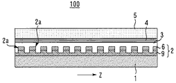
図1は、本発明の実施の形態1にかかる半導体光素子100を示す断面図である。実施の形態1にかかる半導体光素子100は、屈折率結合型の帰還型レーザ素子(DFBレーザ素子)である。半導体光素子100は、半導体基板1と、この半導体基板1の上に順次積層された回折格子2、回折格子埋込層3、活性層4、およびクラッド層5とを備えている。半導体基板1は、Sをドーパントとしたn型InP基板である。なお、半導体基板1は、Znをドーパントとしたp型InP基板としてもよい。
FIG. 1 is a sectional view showing a semiconductor
屈折率結合型の回折格子2は、半導体基板1の上に設けられ、InGaAsP系材料で構成されている。共振器内に備えられた回折格子2は、周期的に屈折率を変化させる。回折格子2を備えることで、共振器内部で複素屈折率の実部のみを周期的に変動させることができ、屈折率結合型の帰還型レーザ素子(DFBレーザ素子)が得られる。回折格子2により複素屈折率の実部のみが周期的に変動し、特定の波長にのみ帰還をかけることができる。回折格子2は、半導体基板1の上においてレーザ光が射出される方向(Z方向)に並ぶ複数の格子片2aを含んでいる。格子片2aそれぞれが、下側部分9および下側部分9の上に設けられた上側部分6とを有する。格子片2aそれぞれの下側部分9が連結しており、回折格子2の下部に1つの層を成している。上側部分6が第1屈折率n1を有し、下側部分9が第2屈折率n2(ただしn2<n1)を有する。上側部分6から下側部分9にかけて段階的に屈折率が低下している。
The refractive index coupled
回折格子埋込層3は、回折格子2を埋め込むように回折格子2に積層され、上側部分6よりも低くかつ下側部分とは異なる屈折率n0を有する。回折格子埋込層3は、InGaAsP系材料からなる。便宜上、回折格子埋込層3の屈折率をn0とし、回折格子2の上側部分6の屈折率をn1とし、回折格子2の下側部分9の屈折率をn2とする。回折格子埋込層3の屈折率n0は、n1とn2の中間である。つまり、n2<n0<n1である。n2<n0<n1の関係が成り立つように、各層の材料組成およびキャリア濃度の少なくとも一方が調整されている。
The diffraction grating buried
活性層4は、回折格子2とともに回折格子埋込層3を挟み込むように回折格子埋込層3に積層されている。活性層4は、回折格子埋込層3の上に積層され、AlInGaAs系もしくはInGaAsP系材料からなる。
The
クラッド層5は、活性層4の上に設けられ、InGaAsP系材料からなる。
The
図2は、実施の形態に対する比較例にかかる半導体光素子400を示す断面図である。比較例にかかる半導体光素子400は、DFB−LDであり、図2の断面図に示すように、上側部分6と下側部分407の二層からなる回折格子408を用いている。上側部分6は実施の形態1と同様であり、その屈折率n1が回折格子埋込層3より高い。一方、下側部分407は回折格子埋込層3と同一の屈折率n0をもつ。
FIG. 2 is a cross-sectional view showing a semiconductor
便宜上、上側部分6と活性層4の距離をtとし、回折格子2、408の深さをdとし、回折格子2、408の周期をΛとし、デューティー比をDとする。製造工程において回折格子埋込層3の成長条件が固定されている場合、回折格子埋込層3の体積が一定であるため、下記の(1)式のような関係が成立する。そのため、回折格子2、408それぞれにおいて、深さdが増加すると距離tが小さくなる。
For convenience, the distance between the
![]()
![]()
図3は、本発明の実施の形態1にかかる半導体光素子100を示す断面図である。図3の断面に示すように、半導体光素子100では回折格子2は高屈折率n1である上側部分6と回折格子埋込層3より低い屈折率n2を持つ下側部分9から構成される。なお、本実施の形態では回折格子2を二層構造としているが、互いに屈折率の異なる三層以上の多層構造としてもよい。回折格子2における実効屈折率差Δnは、上側部分6の厚さをd1、下側部分9の深さをd2とすると加重平均から下記の(2)式のように近似される。d1とd2の合計dが、回折格子2の各格子片2aの高さに一致し、いいかえると回折格子2の隣接する格子片2aの間の溝の深さである。
FIG. 3 is a cross-sectional view showing the semiconductor

光結合係数κは一般に下記の(3)式で表される。k0は波数、βは伝搬定数、Δε1は下記の(4)式で与えられる誘電率の摂動Δε(x,y,z)のフーリエ級数、U(x,y)は光の強度分布である。回折格子2および回折格子408が周期構造をもつ向きをz方向とする。また、一般に誘電率εは屈折率nの二乗に比例する。深さdが大きくなり距離tが小さくなると、活性層4から染み出した光と回折格子2、408とのオーバーラップ量が増える。このため、回折格子2、408への光結合係数κが大きくなる。
The optical coupling coefficient κ is generally expressed by the following equation (3). k 0 is the wave number, beta Fourier series, U (x, y) is the intensity of the light distribution of the propagation constant, [Delta] [epsilon] 1 is the perturbation [Delta] [epsilon] of the dielectric constant given by the following formula (4) (x, y, z) It is. The direction in which the
図4は、本発明の実施の形態1にかかる半導体光素子100の効果を示す図である。図4は、一例として、比較例の半導体光素子400と実施の形態1にかかる半導体光素子100との間で、光結合係数κと共振器長Lの積(κL)と回折格子2、408の深さdの関係をグラフにしたものである。図4に示すとおり、実施の形態1の方が比較例よりもκLの深さd依存性が小さくなっている。κLの深さd依存性が大きければ、深さdの製造バラつきを抑制するために回折格子埋込層3の成長条件を調整することが必要となる。実施の形態1にかかる半導体光素子100はκLの深さd依存性が小さくなるように改善されているので、回折格子埋込層3の成長条件を一定にしても均一な光結合係数κを得やすくなり、DFB−LDの製造効率を上げることができる。回折格子2の製造中におけるバラツキのほかにも、半導体ウェハ面内の傾斜などに起因して回折格子2の深さdにばらつきが生じた場合にも同様に、光結合係数κの面内バラつきを軽減することができる。
FIG. 4 is a diagram showing the effect of the semiconductor
また、本発明では屈折率結合型の回折格子2を用いている。このため、利得結合型回折格子を用いた特許文献1,2に例示される半導体レーザ素子と比較すると、回折格子2における光損失がなく、しきい値電流の上昇、スロープ効率の低下、および消費電力の増大といった特性低下を抑制できるという利点がある。
In the present invention, the refractive index coupled
以上説明した実施の形態1によれば、光結合係数κが回折格子2の深さdに依存して変化する度合いを抑制できる。従って、回折格子埋込層3の成長条件を一定にすることができ、製造効率を上げることができる。
According to the first embodiment described above, the degree to which the optical coupling coefficient κ changes depending on the depth d of the
なお、変形例として、回折格子埋込層3の屈折率n0を下側部分9の屈折率n2より低くしてもよく(すなわちn0<n2)、そのような低屈折率材料に回折格子埋込層3の材料を置換してもよい。この場合、屈折率は、n0<n2<n1という関係になる。この変形を行った場合にも、(2)式において回折格子2の深さdが深くなった場合、(2)式第3項によりΔnが小さくなる。
As a modification, the refractive index n 0 of the diffraction grating buried
実施の形態1では、下側部分9と上側部分6とで二段階に屈折率を変化させた。しかしながら本発明はこれに限られず、三段階、四段階、あるいはそれ以上の段階で上側部分6から下側部分9に徐々に屈折率を低下させてもよい。例えば、半導体光素子100は、下側部分9と上側部分6との間に、下側部分9の屈折率と上側部分6の屈折率との中間の屈折率を有する中間部分を含んでいてもよい。この中間部分をさらに2層、3層あるいはそれ以上の多層構造として、上側部分6から下側部分9に徐々に屈折率を低下させるように回折格子2を複数の層に構成してもよい。
In the first embodiment, the refractive index is changed in two steps between the
図5は、本発明の実施の形態1の変形例にかかる半導体光素子101を示す断面図である。格子片2aは、連続的に屈折率が変化するものであってもよい。図5のように、最上部から最下部にかけて連続的に屈折率が低下する回折格子19を設けて、他の構造は実施の形態1と同じものとしてもよい。このときの回折格子19の最下部の屈折率は回折格子埋込層3よりも低いものとする。この変形を行った場合にも、(2)式において回折格子19の深さdが大きくなると(2)式第3項によりΔnが小さくなるため、上記実施の形態1にかかる半導体光素子100と同じく光結合係数κの変動を抑制する効果が得られる。
FIG. 5 is a cross-sectional view showing a semiconductor
図6は、本発明の実施の形態1の変形例にかかる半導体光素子150を示す断面図である。半導体光素子150は、実施の形態1にかかる半導体光素子100の活性層4を、光導波路層41に置き換えたものである。光導波路層41は、回折格子2とともに回折格子埋込層3を挟み込むように回折格子埋込層3に積層されている。光導波路層41は、InGaAsP系またはAlInGaAs系材料で構成してもよい。これにより、半導体レーザ素子に代えて、結合導波路、波長フィルタを含む導波路型光デバイスを得ることができる。(2)式において回折格子2の深さdが増加した場合に(2)式第3項によりΔnが小さくなるのは半導体光素子150でも同様であるため、光結合係数κのばらつきを抑制できる。なお、回折格子2、回折格子埋込層3、および光導波路層41には、InGaAs、InGaAsP、あるはSiを含む半導体材料を用いてもよく、ポリマー又はSiO2のようなパッシブ材料を用いてもよい。
FIG. 6 is a cross-sectional view showing a semiconductor
実施の形態2.
図7は、本発明の実施の形態2にかかる半導体光素子200を示す断面図である。半導体光素子200は、回折格子2を回折格子22に置換した点を除き、実施の形態1と同様の構成を備えている。回折格子22は、上側部分6と、下側部分9に代えて設けられた下側部分210とを備えるものであり、Z方向に向かって回折格子片22aが並べられたものである。
FIG. 7 is a sectional view showing a semiconductor
下側部分210は上側部分6よりもエッチングレートが低い材料で形成される。この低エッチングレート材料には、AlGaInAsが含まれる。この低エッチングレート材料のエッチングレートは、上側部分6の材料のエッチングレートの例えば1/10以下であることが好ましい。下側部分210は上側部分6よりもエッチングレートが低いので、製造時に回折格子22の深さdが設計値から変動しにくい。従って、回折格子22の深さdがばらつくことに起因する光結合係数κのばらつきを抑制することができる。また、面内の回折格子22の深さdのばらつきも軽減することができるという利点もある。
The
なお、実施の形態2にかかる半導体光素子200において、図6に示した実施の形態1の変形例と同様に、活性層4を光導波路層41に置換してもよい。
In the semiconductor
実施の形態3.
図8は、本発明の実施の形態3にかかる面発光半導体光素子300を示す分解斜視図である。図8では埋込層303と二次元周期構造層330とを分離して図示しているが、実際の面発光半導体光素子300ではこれらの層は密着している。面発光半導体光素子300は、面発光レーザ素子(VCSEL)である。面発光半導体光素子300は、二次元周期構造層330と、埋込層303と、活性層304と、クラッド層305と、これらを挟み込む一対のブラッグ反射鏡(DBR)314、315とを備えている。
FIG. 8 is an exploded perspective view showing the surface emitting semiconductor
二次元周期構造層330は、平面方向に周期的な構造を有する層であり、具体例としてはフォトニック結晶である。二次元周期構造層330は二層構造であり、第1屈折率層312と第2屈折率層313とから構成されている。第1屈折率層312は、二層構造の上側(活性層304側)に位置し、屈折率が高い。第2屈折率層313は、二層構造の下側に位置しており、第1屈折率層312よりも屈折率が低い。つまり、活性層304に近い側に位置する第1屈折率層312は、第2屈折率層313よりも高い屈折率の材料で構成される。
The two-dimensional
第1屈折率層312は、複数の凹部311を備えている。複数の凹部311は、第1屈折率層312の平面方向に一定間隔を保って周期的に並んでいる。複数の凹部311は、平面視における輪郭形状、深さ、および断面構造が互いに同一である。ただし、本発明はこれに限定されるものではなく、複数の凹部311の位置、形状、および間隔は適宜に調整されうる。以上のように、二次元周期構造層330は、複数の凹部311を備えることで平面方向に沿って周期的に並ぶ凸凹を備えている。第1屈折率層312は凸側の部分を構成し、第2屈折率層313はこの第1屈折率層312よりも凹側に位置する部分を構成する。
The first refractive index layer 312 includes a plurality of
埋込層303は、第1屈折率層312および第2屈折率層313の上方に、これらを覆うように二次元周期構造層330に積層される。埋込層303により、第1屈折率層312上の周期的な凸凹が埋め込まれる。第2屈折率層313と埋込層303との間では屈折率が異なるように各層の材料などが選定される。
The buried
埋込層303の上に、さらに活性層304およびクラッド層305を順次成長させる。一対のブラッグ反射鏡(DBR)314、315は、二次元周期構造層330、埋込層303、および活性層304を挟み込んでいる。上下のDBR314、315は、InGaAsP系、AlInGaAs系、又はSiを含む半導体材料で構成してもよく、もしくはSiO2又はTa2O5を含む誘電体材料から構成してもよい。
On the buried
上下のDBR314、315で光を共振させるとともに、活性層304の下の埋め込み二次元周期構造層330の二次元回折を用いることにより、出射ビーム形状をドーナッツ状に変化させたり、出射角度をつけたりすることができる。二次元周期構造層330は、平面方向に周期的に屈折率を変化させる。二次元周期構造層330を備えることで、共振器内部で複素屈折率の実部のみを周期的に変動させることができ、屈折率結合型の面発光型レーザ素子が得られる。二次元周期構造層330の上部に第1屈折率層312を設け下部に第2屈折率層313を設けているので、面内における二次元周期構造層330の凸凹深さが変わることで二次元周期構造層330と活性層304との距離がばらつくことに起因する光結合係数κのばらつきを、実施の形態1と同様に抑制することができる。なお、変形例として、上下のブラッグ反射鏡314、315を省略しても良く、これにより面発光ダイオード(LED)とすることも可能である。
The upper and lower DBRs 314 and 315 resonate light, and the two-dimensional diffraction of the embedded two-dimensional
1 半導体基板、2、19、22、408 回折格子、2a,22a 格子片、3 回折格子埋込層、4、304 活性層、5、305 クラッド層、6 上側部分、9、210、407 下側部分、41 光導波路層、100、101、150、200、400 半導体光素子、300 面発光半導体光素子、303 埋込層、311 凹部、312 第1屈折率層、313 第2屈折率層、314,315 ブラッグ反射鏡、330 二次元周期構造層
DESCRIPTION OF
Claims (2)
前記半導体基板の上に並ぶ複数の格子片を含み、前記格子片それぞれが前記半導体基板の上に設けられた下側部分および前記下側部分の上に設けられた上側部分を含み、前記上側部分が第1屈折率を有し、前記下側部分が前記第1屈折率よりも低い第2屈折率を有し、前記上側部分から前記下側部分にかけて段階的、または連続的に屈折率が低下する、屈折率結合型の回折格子と、
前記回折格子を埋め込むように前記回折格子に積層され、前記第1屈折率よりも低くかつ前記第2屈折率より高い屈折率を有する回折格子埋込層と、
前記回折格子とともに前記回折格子埋込層を挟み込むように前記回折格子埋込層に積層された、活性層または光導波路層と、
を備える半導体光素子。 A semiconductor substrate;
A plurality of lattice pieces arranged on the semiconductor substrate, each lattice piece including a lower portion provided on the semiconductor substrate and an upper portion provided on the lower portion; There has a first refractive index, the lower portion have a second refractive index lower than the first refractive index, stepwise, or continuously refractive index toward the lower portion from the upper portion decreases A refractive index coupled diffraction grating;
Said laminated on the diffraction grating so as to fill the diffraction grating, the diffraction grating burying layer having a refractive index higher than low and the second refractive index than the first refractive index,
An active layer or an optical waveguide layer laminated on the diffraction grating embedded layer so as to sandwich the diffraction grating embedded layer together with the diffraction grating; and
A semiconductor optical device comprising:
Priority Applications (3)
| Application Number | Priority Date | Filing Date | Title |
|---|---|---|---|
| JP2014241903A JP6331997B2 (en) | 2014-11-28 | 2014-11-28 | Semiconductor optical device |
| US14/799,087 US9685764B2 (en) | 2014-11-28 | 2015-07-14 | Semiconductor optical element and surface-emitting semiconductor optical element |
| CN201510849909.9A CN105655868B (en) | 2014-11-28 | 2015-11-27 | Semiconductor laser and surface luminous semiconductor optical element |
Applications Claiming Priority (1)
| Application Number | Priority Date | Filing Date | Title |
|---|---|---|---|
| JP2014241903A JP6331997B2 (en) | 2014-11-28 | 2014-11-28 | Semiconductor optical device |
Publications (3)
| Publication Number | Publication Date |
|---|---|
| JP2016103594A JP2016103594A (en) | 2016-06-02 |
| JP2016103594A5 JP2016103594A5 (en) | 2017-02-09 |
| JP6331997B2 true JP6331997B2 (en) | 2018-05-30 |
Family
ID=56079776
Family Applications (1)
| Application Number | Title | Priority Date | Filing Date |
|---|---|---|---|
| JP2014241903A Active JP6331997B2 (en) | 2014-11-28 | 2014-11-28 | Semiconductor optical device |
Country Status (3)
| Country | Link |
|---|---|
| US (1) | US9685764B2 (en) |
| JP (1) | JP6331997B2 (en) |
| CN (1) | CN105655868B (en) |
Families Citing this family (11)
| Publication number | Priority date | Publication date | Assignee | Title |
|---|---|---|---|---|
| DE112016001195T5 (en) | 2015-03-13 | 2017-11-23 | Hamamatsu Photonics K.K. | LIGHT-EMITTING SEMICONDUCTOR ELEMENT |
| JP6468180B2 (en) * | 2015-12-24 | 2019-02-13 | 三菱電機株式会社 | Manufacturing method of optical semiconductor device |
| WO2017132283A1 (en) * | 2016-01-25 | 2017-08-03 | The Regents Of The University Of California | Nano-scale pixelated filter-free color detector |
| DE102017100997A1 (en) | 2017-01-19 | 2018-07-19 | Osram Opto Semiconductors Gmbh | Semiconductor laser and method for producing such a semiconductor laser |
| CN109962406B (en) * | 2017-12-14 | 2021-11-12 | 中国科学院半导体研究所 | Semiconductor laser and preparation method thereof |
| CN108933382B (en) * | 2018-06-21 | 2019-12-20 | 武汉光迅科技股份有限公司 | Grating, DBR laser and grating preparation method |
| CN111769437B (en) * | 2020-07-21 | 2021-09-21 | 厦门市三安集成电路有限公司 | Bragg grating, preparation method thereof and distributed feedback laser |
| US20220109287A1 (en) * | 2020-10-01 | 2022-04-07 | Vixar, Inc. | Metalens Array and Vertical Cavity Surface Emitting Laser Systems and Methods |
| CN112117640B (en) * | 2020-11-02 | 2022-02-22 | 北京工业大学 | VCSEL (vertical cavity surface emitting laser) light splitting structure of substrate type diffractive optical element and preparation method |
| US20220352693A1 (en) * | 2021-04-30 | 2022-11-03 | Lumentum Operations Llc | Methods for incorporating a control structure within a vertical cavity surface emitting laser device cavity |
| CN113745968B (en) * | 2021-08-27 | 2023-06-30 | 因林光电科技(苏州)有限公司 | Semiconductor laser and preparation method thereof |
Family Cites Families (16)
| Publication number | Priority date | Publication date | Assignee | Title |
|---|---|---|---|---|
| JPH0529705A (en) | 1991-07-22 | 1993-02-05 | Hikari Keisoku Gijutsu Kaihatsu Kk | Distributed feedback type semiconductor laser apparatus |
| DE69117488T2 (en) | 1990-10-19 | 1996-10-02 | Optical Measurement Technology | SEMICONDUCTOR LASER WITH DISTRIBUTED FEEDBACK |
| EP0706243A3 (en) * | 1994-09-28 | 1996-11-13 | Matsushita Electric Ind Co Ltd | Distributed feedback semiconductor laser and method for producing the same |
| JP2924714B2 (en) * | 1995-06-19 | 1999-07-26 | 日本電気株式会社 | Distributed feedback semiconductor laser device |
| JP3140788B2 (en) * | 1995-12-28 | 2001-03-05 | 松下電器産業株式会社 | Semiconductor laser device |
| JP2000349394A (en) * | 1999-06-02 | 2000-12-15 | Matsushita Electric Ind Co Ltd | Semiconductor laser device |
| JP2001168455A (en) * | 1999-12-06 | 2001-06-22 | Fujitsu Ltd | Manufacturing method for optical semiconductor device |
| US6560259B1 (en) * | 2000-05-31 | 2003-05-06 | Applied Optoelectronics, Inc. | Spatially coherent surface-emitting, grating coupled quantum cascade laser with unstable resonance cavity |
| US6365428B1 (en) * | 2000-06-15 | 2002-04-02 | Sandia Corporation | Embedded high-contrast distributed grating structures |
| JP3745985B2 (en) | 2001-01-24 | 2006-02-15 | 古河電気工業株式会社 | Complex coupled type distributed feedback semiconductor laser device |
| CN100568031C (en) * | 2003-03-31 | 2009-12-09 | 日本电信电话株式会社 | Optical semiconductor photoreactive semiconductor integrated circuit |
| JP4358583B2 (en) * | 2003-09-12 | 2009-11-04 | 株式会社ミツトヨ | Scale manufacturing method |
| JP4350774B2 (en) * | 2007-07-31 | 2009-10-21 | キヤノン株式会社 | Surface emitting laser |
| US8201268B1 (en) * | 2008-11-13 | 2012-06-12 | Optonet Inc. | Integrated high index contrast sub-wavelength optical transforming tip (HICSWOTT) for near-field scanning optical microscope |
| DE102009001505A1 (en) * | 2008-11-21 | 2010-05-27 | Vertilas Gmbh | Surface emitting semiconductor laser diode and method of making the same |
| US8343878B2 (en) * | 2008-12-19 | 2013-01-01 | The Board Of Trustees Of The University Of Illinois | Method of plasma etching GA-based compound semiconductors |
-
2014
- 2014-11-28 JP JP2014241903A patent/JP6331997B2/en active Active
-
2015
- 2015-07-14 US US14/799,087 patent/US9685764B2/en active Active
- 2015-11-27 CN CN201510849909.9A patent/CN105655868B/en active Active
Also Published As
| Publication number | Publication date |
|---|---|
| US9685764B2 (en) | 2017-06-20 |
| CN105655868A (en) | 2016-06-08 |
| CN105655868B (en) | 2019-02-19 |
| JP2016103594A (en) | 2016-06-02 |
| US20160156154A1 (en) | 2016-06-02 |
Similar Documents
| Publication | Publication Date | Title |
|---|---|---|
| JP6331997B2 (en) | Semiconductor optical device | |
| US9431793B2 (en) | Semiconductor laser device | |
| US20070242715A1 (en) | Mode and polarization control in vcsels using sub-wavelength structure | |
| US20060215720A1 (en) | Quantum cascade laser with grating formed by a periodic variation in doping | |
| US8638825B2 (en) | Wavelength tunable laser diode | |
| WO2013191745A1 (en) | Photonic crystal surface-emitting lasers enabled by an accidental dirac point | |
| US7912106B2 (en) | Enhanced surface-emitting photonic device | |
| JPWO2008053672A1 (en) | Semiconductor optical device, semiconductor laser using the semiconductor optical device, and optical transponder using the semiconductor laser | |
| JP6807643B2 (en) | Distribution feedback type semiconductor laser device | |
| US12046873B2 (en) | Air cavity dominant VCSELs with a wide wavelength sweep | |
| WO2008103188A1 (en) | High efficiency partial distributed feedback (p-dfb) laser | |
| JP3682367B2 (en) | Distributed feedback laser diode | |
| KR100826732B1 (en) | Surface-emitting type semiconductor laser | |
| KR100594108B1 (en) | Single mode distributed feedback laser | |
| US9093821B2 (en) | Substrate-emitting transverse magnetic polarized laser employing a metal/semiconductor distributed feedback grating for symmetric-mode operation | |
| US10008826B1 (en) | Surface-emitting semiconductor laser | |
| US8351481B2 (en) | Methods and apparatus for single-mode selection in quantum cascade lasers | |
| WO2019013846A2 (en) | Air-cavity dominant vertical cavity surface emitting lasers | |
| JP5702262B2 (en) | Tunable semiconductor laser | |
| JP5681082B2 (en) | Tunable semiconductor laser | |
| JP2012033975A (en) | Method of manufacturing semiconductor laser | |
| JP2010165869A (en) | Semiconductor laser element | |
| US10658816B2 (en) | Distributed feedback laser diode | |
| CN112952551A (en) | Surface emitting laser element with mixed grating structure and manufacturing method thereof | |
| US20160164249A1 (en) | Semiconductor laser diode and laser array implementing the same |
Legal Events
| Date | Code | Title | Description |
|---|---|---|---|
| A521 | Request for written amendment filed |
Free format text: JAPANESE INTERMEDIATE CODE: A523 Effective date: 20161221 |
|
| A621 | Written request for application examination |
Free format text: JAPANESE INTERMEDIATE CODE: A621 Effective date: 20161221 |
|
| A977 | Report on retrieval |
Free format text: JAPANESE INTERMEDIATE CODE: A971007 Effective date: 20170920 |
|
| A131 | Notification of reasons for refusal |
Free format text: JAPANESE INTERMEDIATE CODE: A131 Effective date: 20171003 |
|
| A521 | Request for written amendment filed |
Free format text: JAPANESE INTERMEDIATE CODE: A523 Effective date: 20171127 |
|
| TRDD | Decision of grant or rejection written | ||
| A01 | Written decision to grant a patent or to grant a registration (utility model) |
Free format text: JAPANESE INTERMEDIATE CODE: A01 Effective date: 20180403 |
|
| A61 | First payment of annual fees (during grant procedure) |
Free format text: JAPANESE INTERMEDIATE CODE: A61 Effective date: 20180416 |
|
| R150 | Certificate of patent or registration of utility model |
Ref document number: 6331997 Country of ref document: JP Free format text: JAPANESE INTERMEDIATE CODE: R150 |
|
| R250 | Receipt of annual fees |
Free format text: JAPANESE INTERMEDIATE CODE: R250 |
|
| R250 | Receipt of annual fees |
Free format text: JAPANESE INTERMEDIATE CODE: R250 |
|
| R250 | Receipt of annual fees |
Free format text: JAPANESE INTERMEDIATE CODE: R250 |
|
| R250 | Receipt of annual fees |
Free format text: JAPANESE INTERMEDIATE CODE: R250 |