JP6318708B2 - Ignition control device - Google Patents
Ignition control device Download PDFInfo
- Publication number
- JP6318708B2 JP6318708B2 JP2014043013A JP2014043013A JP6318708B2 JP 6318708 B2 JP6318708 B2 JP 6318708B2 JP 2014043013 A JP2014043013 A JP 2014043013A JP 2014043013 A JP2014043013 A JP 2014043013A JP 6318708 B2 JP6318708 B2 JP 6318708B2
- Authority
- JP
- Japan
- Prior art keywords
- switching element
- side terminal
- ignition
- terminal
- power supply
- Prior art date
- Legal status (The legal status is an assumption and is not a legal conclusion. Google has not performed a legal analysis and makes no representation as to the accuracy of the status listed.)
- Active
Links
- 238000004804 winding Methods 0.000 claims description 89
- 238000004146 energy storage Methods 0.000 claims description 24
- 239000003990 capacitor Substances 0.000 claims description 23
- 238000001514 detection method Methods 0.000 claims description 18
- 239000000446 fuel Substances 0.000 claims description 9
- 239000004065 semiconductor Substances 0.000 claims description 7
- 239000000203 mixture Substances 0.000 claims description 6
- 230000003247 decreasing effect Effects 0.000 claims description 3
- 239000007789 gas Substances 0.000 description 8
- 238000002485 combustion reaction Methods 0.000 description 7
- 230000004048 modification Effects 0.000 description 7
- 238000012986 modification Methods 0.000 description 7
- 238000010586 diagram Methods 0.000 description 6
- 230000000694 effects Effects 0.000 description 5
- 238000013459 approach Methods 0.000 description 3
- 238000004891 communication Methods 0.000 description 3
- 239000000498 cooling water Substances 0.000 description 3
- 230000003071 parasitic effect Effects 0.000 description 3
- 238000011144 upstream manufacturing Methods 0.000 description 3
- XLYOFNOQVPJJNP-UHFFFAOYSA-N water Substances O XLYOFNOQVPJJNP-UHFFFAOYSA-N 0.000 description 3
- 238000009825 accumulation Methods 0.000 description 2
- 230000015556 catabolic process Effects 0.000 description 2
- 230000000630 rising effect Effects 0.000 description 2
- 239000000567 combustion gas Substances 0.000 description 1
- 239000002826 coolant Substances 0.000 description 1
- 239000000110 cooling liquid Substances 0.000 description 1
- 238000009792 diffusion process Methods 0.000 description 1
- 230000008034 disappearance Effects 0.000 description 1
- 230000005669 field effect Effects 0.000 description 1
- 229910044991 metal oxide Inorganic materials 0.000 description 1
- 150000004706 metal oxides Chemical class 0.000 description 1
- 230000002093 peripheral effect Effects 0.000 description 1
- 238000010992 reflux Methods 0.000 description 1
- 230000001360 synchronised effect Effects 0.000 description 1
Images


Classifications
-
- F—MECHANICAL ENGINEERING; LIGHTING; HEATING; WEAPONS; BLASTING
- F02—COMBUSTION ENGINES; HOT-GAS OR COMBUSTION-PRODUCT ENGINE PLANTS
- F02P—IGNITION, OTHER THAN COMPRESSION IGNITION, FOR INTERNAL-COMBUSTION ENGINES; TESTING OF IGNITION TIMING IN COMPRESSION-IGNITION ENGINES
- F02P3/00—Other installations
- F02P3/02—Other installations having inductive energy storage, e.g. arrangements of induction coils
- F02P3/04—Layout of circuits
- F02P3/0407—Opening or closing the primary coil circuit with electronic switching means
- F02P3/0435—Opening or closing the primary coil circuit with electronic switching means with semiconductor devices
-
- F—MECHANICAL ENGINEERING; LIGHTING; HEATING; WEAPONS; BLASTING
- F02—COMBUSTION ENGINES; HOT-GAS OR COMBUSTION-PRODUCT ENGINE PLANTS
- F02P—IGNITION, OTHER THAN COMPRESSION IGNITION, FOR INTERNAL-COMBUSTION ENGINES; TESTING OF IGNITION TIMING IN COMPRESSION-IGNITION ENGINES
- F02P15/00—Electric spark ignition having characteristics not provided for in, or of interest apart from, groups F02P1/00 - F02P13/00 and combined with layout of ignition circuits
- F02P15/10—Electric spark ignition having characteristics not provided for in, or of interest apart from, groups F02P1/00 - F02P13/00 and combined with layout of ignition circuits having continuous electric sparks
-
- F—MECHANICAL ENGINEERING; LIGHTING; HEATING; WEAPONS; BLASTING
- F02—COMBUSTION ENGINES; HOT-GAS OR COMBUSTION-PRODUCT ENGINE PLANTS
- F02P—IGNITION, OTHER THAN COMPRESSION IGNITION, FOR INTERNAL-COMBUSTION ENGINES; TESTING OF IGNITION TIMING IN COMPRESSION-IGNITION ENGINES
- F02P9/00—Electric spark ignition control, not otherwise provided for
-
- F—MECHANICAL ENGINEERING; LIGHTING; HEATING; WEAPONS; BLASTING
- F02—COMBUSTION ENGINES; HOT-GAS OR COMBUSTION-PRODUCT ENGINE PLANTS
- F02P—IGNITION, OTHER THAN COMPRESSION IGNITION, FOR INTERNAL-COMBUSTION ENGINES; TESTING OF IGNITION TIMING IN COMPRESSION-IGNITION ENGINES
- F02P11/00—Safety means for electric spark ignition, not otherwise provided for
- F02P11/06—Indicating unsafe conditions
Description
本発明は、内燃機関の気筒内にて燃料混合気を点火するように設けられた点火プラグの、動作を制御するように構成された、点火制御装置に関する。 The present invention relates to an ignition control device configured to control the operation of a spark plug provided to ignite a fuel mixture in a cylinder of an internal combustion engine.
この種の装置において、燃料混合気の燃焼状態を良好なものにするために、いわゆる多重放電を行うように構成されたものが知られている。例えば、特開2007−231927号公報には、1回の燃焼行程内にて複数回の放電を断続的に生じさせる構成が開示されている。一方、特開2000−199470号公報には、放電時間の長い多重放電特性を得るために、2つの点火コイルを並列に接続した構成が開示されている。 In this type of apparatus, there is known an apparatus configured to perform so-called multiple discharge in order to improve the combustion state of the fuel mixture. For example, Japanese Patent Application Laid-Open No. 2007-231927 discloses a configuration in which a plurality of discharges are intermittently generated within one combustion stroke. On the other hand, Japanese Patent Laid-Open No. 2000-199470 discloses a configuration in which two ignition coils are connected in parallel in order to obtain multiple discharge characteristics with a long discharge time.
特開2007−231927号公報に記載の構成のように、1回の燃焼行程内にて複数回の放電を断続的に生じさせる場合、当該行程内における点火放電の開始から終了までの間に、点火放電電流が繰り返しゼロとなる。すると、特に筒内のガス流速が大きい場合に、いわゆる「吹き消え」が生じ、点火エネルギがロスされるという問題が生じ得る。一方、特開2000−199470号公報に記載のように、2つの点火コイルを並列に接続した構成においては、1回の燃焼行程内における点火放電の開始から終了までの間に点火放電電流が繰り返しゼロとなることはないものの、装置構成が複雑化し、装置サイズも大型化するという問題がある。また、かかる従来技術においては、点火に必要なエネルギを大きく上回る構成となることで、無駄な電力消費が発生するという問題もある。本発明は、上記に例示した事情等に鑑みてなされたものである。 When a plurality of discharges are intermittently generated in one combustion stroke as in the configuration described in Japanese Patent Laid-Open No. 2007-231927, during the period from the start to the end of the ignition discharge in the stroke, The ignition discharge current repeatedly becomes zero. Then, particularly when the gas flow rate in the cylinder is large, a so-called “blown out” occurs, and there may be a problem that ignition energy is lost. On the other hand, as described in Japanese Patent Application Laid-Open No. 2000-199470, in the configuration in which two ignition coils are connected in parallel, the ignition discharge current is repeatedly generated from the start to the end of the ignition discharge within one combustion stroke. Although it does not become zero, there is a problem that the apparatus configuration becomes complicated and the apparatus size increases. In addition, in the related art, there is a problem that wasteful power consumption occurs due to the configuration that greatly exceeds the energy required for ignition. The present invention has been made in view of the circumstances exemplified above.
本発明の点火制御装置(30)は、点火プラグ(19)の動作を制御するように構成されている。ここで、前記点火プラグは、内燃機関(11)の気筒(11b)内にて燃料混合気を点火するように設けられている。本発明の点火制御装置は、イグニッションコイル(311)と、直流電源(312)と、第一スイッチング素子(313)と、第二スイッチング素子(314)と、第三スイッチング素子(315)と、エネルギ蓄積コイル(316)と、を備えている。 The ignition control device (30) of the present invention is configured to control the operation of the spark plug (19). Here, the spark plug is provided so as to ignite the fuel mixture in the cylinder (11b) of the internal combustion engine (11). The ignition control device of the present invention includes an ignition coil (311), a DC power supply (312), a first switching element (313), a second switching element (314), a third switching element (315), an energy And a storage coil (316).
前記イグニッションコイルは、一次巻線(311a)と、二次巻線(311b)と、を備えている。前記二次巻線は、前記点火プラグに接続されている。このイグニッションコイルは、一次電流(前記一次巻線を通流する電流)の増減により、前記二次巻線にて二次電流が発生するように構成されている。また、前記一次巻線にて前記一次電流を通流させるように、前記一次巻線の一端側には、前記直流電源における非接地側出力端子が接続されている。 The ignition coil includes a primary winding (311a) and a secondary winding (311b). The secondary winding is connected to the spark plug. The ignition coil is configured such that a secondary current is generated in the secondary winding by increasing or decreasing a primary current (current flowing through the primary winding). In addition, an ungrounded output terminal of the DC power supply is connected to one end of the primary winding so that the primary current flows through the primary winding.
前記第一スイッチング素子は、第一制御端子(313G)と、第一電源側端子(313C)と、第一接地側端子(313E)と、を有している。この第一スイッチング素子は、半導体スイッチング素子であって、前記第一制御端子に入力された第一制御信号に基づいて、前記第一電源側端子と前記第一接地側端子との間の通電のオンオフを制御するように構成されている。この第一スイッチング素子においては、前記第一電源側端子は、前記一次巻線の他端側に接続されている。また、前記第一接地側端子は、接地側に接続されている。 The first switching element has a first control terminal (313G), a first power supply side terminal (313C), and a first ground side terminal (313E). The first switching element is a semiconductor switching element, and based on a first control signal input to the first control terminal, an energization between the first power supply side terminal and the first ground side terminal is performed. It is configured to control on / off. In the first switching element, the first power supply side terminal is connected to the other end side of the primary winding. The first ground side terminal is connected to the ground side.
前記第二スイッチング素子は、第二制御端子(314G)と、第二電源側端子(314D)と、第二接地側端子(314S)と、を有している。この第二スイッチング素子は、半導体スイッチング素子であって、前記第二制御端子に入力された第二制御信号に基づいて、前記第二電源側端子と前記第二接地側端子との間の通電のオンオフを制御するように構成されている。この第二スイッチング素子においては、前記第二接地側端子が前記一次巻線の前記他端側に接続されている。 The second switching element has a second control terminal (314G), a second power supply side terminal (314D), and a second ground side terminal (314S). The second switching element is a semiconductor switching element, and based on a second control signal input to the second control terminal, an energization between the second power supply side terminal and the second ground side terminal is performed. It is configured to control on / off. In the second switching element, the second ground side terminal is connected to the other end side of the primary winding.
前記第三スイッチング素子は、第三制御端子(315G)と、第三電源側端子(315C)と、第三接地側端子(315E)と、を有している。この第三スイッチング素子は、半導体スイッチング素子であって、前記第三制御端子に入力された第三制御信号に基づいて、前記第三電源側端子と前記第三接地側端子との間の通電のオンオフを制御するように構成されている。この第三スイッチング素子においては、前記第三電源側端子は、前記第二スイッチング素子における前記第二電源側端子に接続されている。また、前記第三接地側端子は、前記接地側に接続されている。 The third switching element has a third control terminal (315G), a third power supply side terminal (315C), and a third ground side terminal (315E). The third switching element is a semiconductor switching element, and based on a third control signal input to the third control terminal, an energization between the third power supply side terminal and the third ground side terminal is performed. It is configured to control on / off. In the third switching element, the third power supply side terminal is connected to the second power supply side terminal in the second switching element. The third ground side terminal is connected to the ground side.
前記エネルギ蓄積コイルは、前記第三スイッチング素子のオンによってエネルギを蓄積するように設けられたインダクタである。このエネルギ蓄積コイルは、前記直流電源における前記非接地側出力端子と前記第三スイッチング素子における前記第三電源側端子とを接続する電力ラインに介装されている。 The energy storage coil is an inductor provided to store energy when the third switching element is turned on. The energy storage coil is interposed in a power line that connects the non-grounded output terminal of the DC power supply and the third power supply side terminal of the third switching element.
かかる構成を有する本発明の前記点火制御装置においては、前記第一スイッチング素子のオンにより、前記一次巻線に前記一次電流が通流する。これにより、前記イグニッションコイルが充電される。その後、前記第一スイッチング素子がオフされると、それ以前まで前記一次巻線に通流していた前記一次電流が急激に遮断される。すると、前記イグニッションコイルの前記一次巻線に高電圧が発生し、かかる高電圧がさらに前記二次巻線で昇圧されることで、前記点火プラグにて高電圧が発生して放電が発生し、このとき前記二次巻線にて大きな前記二次電流が生じる。これにより、前記点火プラグにて前記点火放電が開始される。 In the ignition control device of the present invention having such a configuration, the primary current flows through the primary winding when the first switching element is turned on. Thereby, the ignition coil is charged. Thereafter, when the first switching element is turned off, the primary current that has been flowing through the primary winding until then is rapidly cut off. Then, a high voltage is generated in the primary winding of the ignition coil, and the high voltage is further boosted in the secondary winding, so that a high voltage is generated in the spark plug and a discharge is generated. At this time, a large secondary current is generated in the secondary winding. Thereby, the ignition discharge is started by the spark plug.
ここで、前記点火プラグにて前記点火放電が開始した後は、前記二次電流(以下「放電電流」と称する)は、そのままでは時間経過とともにゼロに近づく。この点、本発明の構成においては、前記点火放電中に前記第二スイッチング素子がオンされることで、当該第二スイッチング素子を介して、エネルギが前記他端側から前記一次巻線に供給される。すると、前記一次電流が通流する。このとき、それまで通流していた前記放電電流に対して、かかる一次電流の通流に伴う追加分が重畳される。すると、前記一次巻線に流れる電流が増強され、前記二次巻線に放電維持電圧以上の誘導起電力を発生させることができる。このため、前記二次電流すなわち前記放電電流が増強され、以て吹き消えを効果的に抑制することができる。これにより、前記放電電流が、前記点火放電を維持可能な程度に良好に確保される。 Here, after the ignition discharge is started by the spark plug, the secondary current (hereinafter referred to as “discharge current”) approaches zero as time passes. In this regard, in the configuration of the present invention, when the second switching element is turned on during the ignition discharge, energy is supplied to the primary winding from the other end side via the second switching element. The Then, the primary current flows. At this time, an additional portion accompanying the flow of the primary current is superimposed on the discharge current that has been flowing so far. Then, the current flowing through the primary winding is increased, and an induced electromotive force higher than the discharge sustaining voltage can be generated in the secondary winding. For this reason, the secondary current, that is, the discharge current is enhanced, and blowout can be effectively suppressed. As a result, the discharge current is ensured satisfactorily to such an extent that the ignition discharge can be maintained.
したがって、本発明によれば、いわゆる「吹き消え」の発生及びこれに伴う点火エネルギのロスが、簡略な装置構成によって良好に抑制される。また、このように前記一次巻線の低圧側(接地側あるいは前記第一スイッチング側)からエネルギを投入することにより、前記二次巻線側からエネルギを投入する場合よりも、低圧でエネルギを投入することが可能となる。この点、前記一次巻線の高圧側(前記直流電源側)から、前記直流電源の電圧より高い電圧でエネルギ投入すると、当該直流電源への流入電流などにより効率が悪くなる。これに対し、本発明によれば、上述のように、前記一次巻線の低圧側からエネルギを投入するため、もっとも容易に効率よくエネルギを投入することができるという優れた効果がある。 Therefore, according to the present invention, the occurrence of so-called “blown out” and the resulting loss of ignition energy are satisfactorily suppressed by a simple device configuration. In addition, by supplying energy from the low-voltage side (grounding side or the first switching side) of the primary winding in this way, energy is input at a lower pressure than when energy is input from the secondary winding side. It becomes possible to do. In this regard, if energy is input from the high voltage side (the DC power supply side) of the primary winding at a voltage higher than the voltage of the DC power supply, the efficiency is deteriorated due to an inflow current to the DC power supply. On the other hand, according to the present invention, as described above, since energy is input from the low-voltage side of the primary winding, there is an excellent effect that energy can be input most easily and efficiently.
以下、本発明を具体化した一実施形態を、図面を参照しつつ説明する。なお、変形例は、当該実施形態の説明中に挿入されると首尾一貫した一実施形態の説明の理解が妨げられるので、末尾にまとめて記載されている。 DESCRIPTION OF EXEMPLARY EMBODIMENTS Hereinafter, an embodiment of the invention will be described with reference to the drawings. In addition, since a modification will prevent understanding of description of one consistent embodiment, if it is inserted during the description of the said embodiment, it is described collectively at the end.
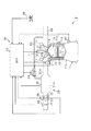
<エンジンシステムの構成>
図1を参照すると、エンジンシステム10は、火花点火式の内燃機関であるエンジン11を備えている。エンジン11の本体部を構成するエンジンブロック11aの内部には、気筒11b及びウォータージャケット11cが形成されている。気筒11bは、ピストン12を往復移動可能に収容するように設けられている。ウォータージャケット11cは、冷却液(冷却水ともいう)が通流可能な空間であって、気筒11bの周囲を取り囲むように設けられている。
<Engine system configuration>
Referring to FIG. 1, an
エンジンブロック11aの上部であるシリンダヘッドには、吸気ポート13及び排気ポート14が、気筒11bと連通可能に形成されている。また、シリンダヘッドには、吸気ポート13と気筒11bとの連通状態を制御するための吸気バルブ15と、排気ポート14と気筒11bとの連通状態を制御するための排気バルブ16と、吸気バルブ15及び排気バルブ16を所定のタイミングで開閉動作させるためのバルブ駆動機構17と、が設けられている。
An
さらに、エンジンブロック11aには、インジェクタ18及び点火プラグ19が装着されている。本実施形態においては、インジェクタ18は、気筒11b内に燃料を直接噴射するように設けられている。点火プラグ19は、気筒11b内にて燃料混合気を点火するように設けられている。
Further, an
エンジン11には、給排気機構20が接続されている。給排気機構20には、吸気管21(吸気マニホールド21a及びサージタンク21bを含む)と、排気管22と、EGR通路23と、の3種類のガス通路が設けられている。
A supply /
吸気マニホールド21aは、吸気ポート13に接続されている。サージタンク21bは、吸気マニホールド21aよりも吸気通流方向における上流側に配置されている。排気管22は、排気ポート14に接続されている。
The
EGR通路23は、排気管22とサージタンク21bとを接続することで、排気管22に排出された排気ガスの一部を吸気に導入可能に設けられている(EGRはExhaust Gas Recirculationの略である)。EGR通路23には、EGR制御バルブ24が介装されている。EGR制御バルブ24は、その開度によってEGR率(気筒11b内に吸入される燃焼前のガスにおける排気ガスの混入割合)を制御可能に設けられている。
The
吸気管21における、サージタンク21bよりも吸気通流方向における上流側には、スロットルバルブ25が介装されている。スロットルバルブ25は、その開度が、DCモータ等のスロットルアクチュエータ26の動作によって制御されるようになっている。また、吸気ポート13の近傍には、スワール流やタンブル流を発生させるための気流制御バルブ27が設けられている。
A
エンジンシステム10には、点火制御装置30が設けられている。点火制御装置30は、点火プラグ19の動作を制御する(すなわちエンジン11における点火制御を行う)ように構成されている。この点火制御装置30は、点火回路ユニット31と、電子制御ユニット32と、を備えている。
The
点火回路ユニット31は、気筒11b内の燃料混合気に点火するための火花放電を点火プラグ19にて発生させるように構成されている。電子制御ユニット32は、いわゆるエンジンECU(ECUはElectronic Control Unitの略である)であって、回転速度センサ33等の各種センサの出力に基づいて取得したエンジン11の運転状態(以下「エンジンパラメータ」と略称する。)に応じて、インジェクタ18及び点火回路ユニット31を含む各部の動作を制御するようになっている。
The
点火制御に関しては、電子制御ユニット32は、取得したエンジンパラメータに基づいて、点火信号IGt及びエネルギ投入期間信号IGwを生成及び出力するようになっている。かかる点火信号IGt及びエネルギ投入期間信号IGwは、気筒11b内のガスの状態及び必要とされるエンジン11の出力(これらはエンジンパラメータに応じて変化する)に応じた、最適な点火時期及び放電電流(点火放電電流)を規定するものである。なお、これらの信号についてはすでに公知あるいは周知であるので、これらの信号についてのこれ以上の詳細な説明については本明細書では省略する(必要に応じ、特開2002−168170号公報、特開2007−211631号公報、等参照。)。
Regarding the ignition control, the
回転速度センサ33は、エンジン回転速度(エンジン回転数ともいう)Neを検出(取得)するためのセンサである。この回転速度センサ33は、ピストン12の往復運動に伴って回転する図示しないクランクシャフトの回転角度に応じたパルス状の出力を生じるように、エンジンブロック11aに装着されている。冷却水温センサ34は、ウォータージャケット11c内を通流する冷却液の温度である冷却水温Twを検出(取得)するためのセンサであって、エンジンブロック11aに装着されている。
The
エアフローメータ35は、吸入空気量Ga(吸気管21を通流して気筒11b内に導入される吸入空気の質量流量)を検出(取得)するためのセンサである。このエアフローメータ35は、スロットルバルブ25よりも吸気通流方向における上流側にて、吸気管21に装着されている。吸気圧センサ36は、吸気管21内の圧力である吸気圧Paを検出(取得)するためのセンサであって、サージタンク21bに装着されている。
The
スロットル開度センサ37は、スロットルバルブ25の開度(スロットル開度THA)に対応する出力を生じるセンサであって、スロットルアクチュエータ26に内蔵されている。アクセルポジションセンサ38は、図示しないアクセルの操作量(アクセル操作量ACCP)に対応する出力を生じるように設けられている。
The throttle opening sensor 37 is a sensor that generates an output corresponding to the opening of the throttle valve 25 (throttle opening THA), and is built in the
<第一実施形態の点火制御装置の構成>
図2を参照すると、第一実施形態における点火回路ユニット31は、イグニッションコイル311(一次巻線311a及び二次巻線311bを含む)と、直流電源312と、第一スイッチング素子313と、第二スイッチング素子314と、第三スイッチング素子315と、エネルギ蓄積コイル316と、コンデンサ317と、ダイオード318a,318b及び318cと、ドライバ回路319と、を備えている。
<Configuration of Ignition Control Device of First Embodiment>
Referring to FIG. 2, the
上述のように、イグニッションコイル311は、一次巻線311aと二次巻線311bとを備えている。このイグニッションコイル311は、周知の通り、一次巻線311aを通流する一次電流の増減により、二次巻線311bにて二次電流を発生させるように構成されている。
As described above, the
一次巻線311aの一端である高電圧側端子(非接地側端子とも称し得る)側には、直流電源312における非接地側出力端子(具体的には+端子)が接続されている。一方、一次巻線311aの他端である低電圧側端子(接地側端子とも称し得る)側は、第一スイッチング素子313を介して、接地側に接続されている。すなわち、直流電源312は、第一スイッチング素子313がオンされたときに、一次巻線311aにて高電圧側端子側から低電圧側端子側に向かう方向の一次電流を通流させるように設けられている。
A non-grounded output terminal (specifically, a + terminal) of the
二次巻線311bにおける高電圧側端子(非接地側端子とも称し得る)側は、ダイオード318aを介して、一次巻線311aにおける高電圧側端子側に接続されている。このダイオード318aは、一次巻線311aにおける高電圧側端子側から二次巻線311bにおける高電圧側端子側に向かう方向の電流の通流を禁止するとともに、二次電流(放電電流)を点火プラグ19から二次巻線311bに向かう(すなわち図中の電流I2が負の値となる)方向に規定すべく、そのアノードが二次巻線311bにおける高電圧側端子側に接続されている。一方、二次巻線311bにおける低電圧側端子(接地側端子とも称し得る)側は、点火プラグ19に接続されている。
The high voltage side terminal (which may also be referred to as a non-ground side terminal) side in the secondary winding 311b is connected to the high voltage side terminal side in the primary winding 311a via a
第一スイッチング素子313は、MOSゲート構造トランジスタであるIGBT(IGBTはInsulated Gate Bipolar Transistorの略)であって、第一制御端子313Gと、第一電源側端子313Cと、第一接地側端子313Eと、を有している。この第一スイッチング素子313は、第一制御端子313Gに入力された第一制御信号IGaに基づいて、第一電源側端子313Cと第一接地側端子313Eとの間の通電のオンオフを制御するように構成されている。本実施形態においては、第一電源側端子313Cは、一次巻線311aにおける低電圧側端子側に接続されている。また、第一接地側端子313Eは、接地側に接続されている。
The
第二スイッチング素子314は、MOSFET(MOSFETはMetal Oxide Semiconductor Field Effect Transistorの略)であって、第二制御端子314Gと、第二電源側端子314Dと、第二接地側端子314Sと、を有している。この第二スイッチング素子314は、第二制御端子314Gに入力された第二制御信号IGbに基づいて、第二電源側端子314Dと第二接地側端子314Sとの間の通電のオンオフを制御するように構成されている。
The
本実施形態においては、第二接地側端子314Sは、ダイオード318bを介して、一次巻線311aにおける低電圧側端子側に接続されている。このダイオード318bは、第二スイッチング素子314における第二接地側端子314Sから一次巻線311aにおける低電圧側端子側に向かう方向の電流の通流を許容するように、そのアノードが第二接地側端子314Sに接続されている。
In the present embodiment, the second
第三スイッチング素子315は、MOSゲート構造トランジスタであるIGBTであって、第三制御端子315Gと、第三電源側端子315Cと、第三接地側端子315Eと、を有している。この第三スイッチング素子315は、第三制御端子315Gに入力された第三制御信号IGcに基づいて、第三電源側端子315Cと第三接地側端子315Eとの間の通電のオンオフを制御するように構成されている。
The
本実施形態においては、第三電源側端子315Cは、ダイオード318cを介して、第二スイッチング素子314における第二電源側端子314Dに接続されている。ダイオード318cは、第三スイッチング素子315における第三電源側端子315Cから第二スイッチング素子314における第二電源側端子314Dに向かう方向の電流の通流を許容するように、そのアノードが第三電源側端子315Cに接続されている。また、第三スイッチング素子315における第三接地側端子315Eは、接地側に接続されている。
In the present embodiment, the third power supply side terminal 315C is connected to the second power
エネルギ蓄積コイル316は、第三スイッチング素子315のオンによってエネルギを蓄積するように設けられたインダクタである。このエネルギ蓄積コイル316は、直流電源312における上述の非接地側出力端子と第三スイッチング素子315における第三電源側端子315Cとを接続する電力ラインに介装されている。
The
コンデンサ317は、接地側と直流電源312における上述の非接地側出力端子との間にて、エネルギ蓄積コイル316と直列接続されている。すなわち、コンデンサ317は、エネルギ蓄積コイル316に対して、第三スイッチング素子315と並列接続されている。このコンデンサ317は、第三スイッチング素子315のオフによって、エネルギを蓄積するように設けられている。
The
本発明の「制御部」を構成するドライバ回路319は、電子制御ユニット32から出力されたエンジンパラメータ、点火信号IGt及びエネルギ投入期間信号IGwを受信するように、電子制御ユニット32に接続されている。また、ドライバ回路319は、第一スイッチング素子313、第二スイッチング素子314、及び第三スイッチング素子315を制御するように、第一制御端子313G、第二制御端子314G及び第三制御端子315Gに接続されている。このドライバ回路319は、受信した点火信号IGt及びエネルギ投入期間信号IGwに基づいて、第一制御信号IGa、第二制御信号IGb、及び第三制御信号IGcを、それぞれ第一制御端子313G、第二制御端子314G及び第三制御端子315Gに出力するように設けられている。
The
具体的には、ドライバ回路319は、点火プラグ19の点火放電(これは第一スイッチング素子313のオフにより開始される)中に、コンデンサ317から蓄積エネルギを放出させる(これは第三スイッチング素子315のオフ及び第二スイッチング素子314のオンにより行われる)ことで一次巻線311aにおける低電圧側端子側から当該一次巻線311aに一次電流を供給すべく、各スイッチング素子を制御するようになっている。特に、本実施形態においては、ドライバ回路319は、コンデンサ317からの蓄積エネルギの蓄積量あるいは放出量をエンジンパラメータに応じて可変とすべく、第二スイッチング素子314及び第三スイッチング素子315を制御するようになっている。
Specifically, the
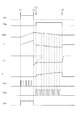
<第一実施形態の動作説明>
以下、本実施形態の構成による動作(作用・効果)について説明する。図3及び図4のタイムチャートにおいて、「Vdc」はコンデンサ317の電圧、「I1」は一次電流、「I2」は二次電流、「P」はコンデンサ317から放出されて一次巻線311aに対してその低電圧側端子側から供給されるエネルギ(以下「投入エネルギ」と称する)、をそれぞれ示す。
<Description of Operation of First Embodiment>
The operation (action / effect) according to the configuration of the present embodiment will be described below. In the time charts of FIGS. 3 and 4, “Vdc” is the voltage of the
なお、図中、一次電流「I1」及び二次電流「I2」のタイムチャートにおいては、図2にて矢印で示されている方向が正の値となるように示されているものとする。また、投入エネルギPのタイムチャートにおいては、1回の点火タイミング中における、供給開始(最初の第二制御信号IGbの立ち上り)からの投入エネルギの積算値が示されている。また、点火信号IGt、エネルギ投入期間信号IGw、第一制御信号IGa、第二制御信号IGb、及び第三制御信号IGcは、図中上方に立ち上がった状態が「H」であり、下方に立ち下がった状態が「L」であるものとする。 In the figure, in the time chart of the primary current “I1” and the secondary current “I2”, it is assumed that the direction indicated by the arrow in FIG. 2 is a positive value. Further, in the time chart of the input energy P, the integrated value of the input energy from the start of supply (rise of the first second control signal IGb) during one ignition timing is shown. Further, the ignition signal IGt, the energy input period signal IGw, the first control signal IGa, the second control signal IGb, and the third control signal IGc are “H” in the state of rising upward in the drawing and falling downward. It is assumed that the status is “L”.
電子制御ユニット32は、回転速度センサ33等の各種センサの出力に基づいて取得したエンジンパラメータに応じて、インジェクタ18及び点火回路ユニット31を含む、エンジンシステム10における各部の動作を制御する。ここで、点火制御について詳述すると、電子制御ユニット32は、取得したエンジンパラメータに基づいて、点火信号IGt及びエネルギ投入期間信号IGwを生成する。そして、電子制御ユニット32は、生成した点火信号IGt及びエネルギ投入期間信号IGwと、エンジンパラメータとを、ドライバ回路319に向けて出力する。
The
ドライバ回路319は、電子制御ユニット32から出力された点火信号IGt、エネルギ投入期間信号IGw及びエンジンパラメータを受信すると、これらに基づいて、第一スイッチング素子313のオンオフを制御するための第一制御信号IGa、第二スイッチング素子314のオンオフを制御するための第二制御信号IGb、及び第三スイッチング素子315のオンオフを制御するための第三制御信号IGcを出力する。
When the
なお、本実施形態においては、第一制御信号IGaは、点火信号IGtと同一である。このため、ドライバ回路319は、受信した点火信号IGtをそのまま第一スイッチング素子313における第一制御端子313Gに向けて出力する。
In the present embodiment, the first control signal IGa is the same as the ignition signal IGt. For this reason, the
一方、第二制御信号IGbは、受信したエネルギ投入期間信号IGwに基づいて生成されるものである。このため、ドライバ回路319は、受信したエネルギ投入期間信号IGwに基づいて第二制御信号IGbを生成するとともに、かかる第二制御信号IGbを第二スイッチング素子314における第二制御端子314Gに向けて出力する。なお、本実施形態においては、第二制御信号IGbは、エネルギ投入期間信号IGwがHレベルの間に繰り返し出力される、周期及びオンデューティ比が一定(1:1)の矩形波パルス状の信号である。
On the other hand, the second control signal IGb is generated based on the received energy input period signal IGw. Therefore, the
また、第三制御信号IGcは、受信した点火信号IGt及びエンジンパラメータに基づいて生成されるものである。このため、ドライバ回路319は、受信した点火信号IGt及びエンジンパラメータに基づいて第三制御信号IGcを生成するとともに、かかる第三制御信号IGcを第三スイッチング素子315における第三制御端子315Gに向けて出力する。なお、本実施形態においては、第三制御信号IGcは、点火信号IGtがHレベルの間に繰り返し出力される、周期が一定でエンジンパラメータに基づいてオンデューティ比が可変とされる矩形波パルス状の信号である。
The third control signal IGc is generated based on the received ignition signal IGt and engine parameters. Therefore, the
以下図3を参照すると、時刻t1にて点火信号IGtがHレベルに立ち上がると、これに対応して、第一制御信号IGaがHレベルに立ち上げられることで、第一スイッチング素子313がオンされる(このときエネルギ投入期間信号IGwはLレベルであるため第二スイッチング素子314はオフである)。これにより、一次巻線311aにおける一次電流の通流が開始する。
Referring to FIG. 3 below, when the ignition signal IGt rises to H level at time t1, the
また、点火信号IGtがHレベルに立ち上がっている間、矩形波パルス状の第三制御信号IGcが、第三スイッチング素子315における第三制御端子315Gに入力される。すると、第三スイッチング素子315のオンオフにおけるオン後のオフ期間(すなわち第三制御信号IGcにおけるLレベル期間中)に、電圧Vdcがステップ状に上昇する。
Further, while the ignition signal IGt rises to the H level, the third control signal IGc in the form of a rectangular pulse is input to the
このようにして、点火信号IGtがHレベルに立ち上がっている時刻t1−t2間に、イグニッションコイル311が充電されるとともに、エネルギ蓄積コイル316を介してコンデンサ317にエネルギが蓄積される。かかるエネルギの蓄積は、時刻t2までに終了する。
Thus, the
その後、時刻t2にて第一制御信号IGaがHレベルからLレベルに立ち下げられることで、第一スイッチング素子313がオフされると、それ以前まで一次巻線311aに通流していた一次電流が急激に遮断される。すると、イグニッションコイル311が放電し、二次巻線311bにて、大きな二次電流である放電電流が生じる。これにより、点火プラグ19にて点火放電が開始する。
After that, when the
時刻t2にて点火放電が開始した後は、従来の放電制御においては(あるいはエネルギ投入期間信号IGwがHレベルに立ち上げられることなくLレベルのまま維持されるような運転条件においては)、破線で示されたように、放電電流はそのままでは時間経過とともにゼロに近づき、放電を維持できない程度まで減衰し放電は終了する。 After ignition discharge starts at time t2, in conventional discharge control (or under operating conditions in which the energy input period signal IGw is maintained at L level without being raised to H level), a broken line As shown in the above, the discharge current approaches zero as time elapses as it is, decays to such an extent that the discharge cannot be maintained, and the discharge ends.
この点、本動作例においては、時刻t2の直後の時刻t3にてエネルギ投入期間信号IGwがHレベルに立ち上げられることで、第三スイッチング素子315のオフ(第三制御信号IGc=Lレベル)下で第二スイッチング素子314がオンされる(第二制御信号IGb=Hレベル)。すると、コンデンサ317の蓄積エネルギが当該コンデンサ317から放出され、上述の投入エネルギが、一次巻線311aに対してその低電圧側端子側から供給される。これにより、点火放電中に、投入エネルギに起因する一次電流が通流する。
In this regard, in this operation example, the energy input period signal IGw is raised to H level at time t3 immediately after time t2, so that the
このとき、時刻t2−t3間で通流していた放電電流に対して、投入エネルギに起因する一次電流の通流に伴う追加分が重畳される。かかる一時電流の重畳(追加)は、時刻t3以降(t4まで)、第二スイッチング素子314がオンされる毎に行われる。すなわち、図3に示されているように、第二制御信号IGbが立ち上がる毎に、コンデンサ317の蓄積エネルギにより一次電流(I1)が順次追加され、これに対応して、放電電流(I2)が順次追加される。これにより、放電電流が、点火放電を維持可能な程度に良好に確保される。なお、本具体例においては、時刻t2とt3との間の時間間隔は、いわゆる「吹き消え」が生じないように、エンジン回転速度Ne及び吸入空気量Gaに基づいて電子制御ユニット32により適宜(マップ等を用いて)設定されるものとする。
At this time, the additional amount accompanying the flow of the primary current due to the input energy is superimposed on the discharge current that has been flowing between the times t2 and t3. The superimposition (addition) of the temporary current is performed every time the
ところで、点火信号IGtがHレベルに立ち上がっている時刻t1−t2間における、コンデンサ317におけるエネルギ蓄積状態は、第三制御信号IGcのオンデューティ比によって制御可能である。また、コンデンサ317における蓄積エネルギが大きいほど、第二スイッチング素子314がオンされる毎の投入エネルギもまた大きくなる。
By the way, the energy storage state in the
そこで、本実施形態においては、いわゆる「吹き消え」が生じやすい高負荷又は高回転運転条件(吸気圧Pa:高、エンジン回転速度Ne:高、スロットル開度THA:大、EGR率:高、空燃比:リーン)になるほど、第三制御信号IGcのオンデューティ比が高く設定される。これにより、エンジンの運転状態に合わせて図4に示されているように(特に図4における矢印参照)、コンデンサ317におけるエネルギ蓄積量や投入エネルギを高めることができ、電力消費をおさえながら「吹き消え」を良好に抑制することが可能となる。
Therefore, in the present embodiment, a high load or high rotation operation condition in which so-called “blown out” is likely to occur (intake pressure Pa: high, engine rotation speed Ne: high, throttle opening THA: high, EGR rate: high, empty The on-duty ratio of the third control signal IGc is set higher as the fuel ratio becomes leaner. As a result, as shown in FIG. 4 according to the operating state of the engine (see particularly the arrow in FIG. 4), the amount of energy stored in the
このように、本実施形態の構成においては、いわゆる「吹き消え」が生じないように放電電流の通流状態を、気筒11b内におけるガスの流動状態に対応して良好に制御することが可能となる。したがって、本実施形態によれば、いわゆる「吹き消え」の発生及びこれに伴う点火エネルギのロスが、簡略な装置構成によって良好に抑制される。 As described above, in the configuration of the present embodiment, it is possible to satisfactorily control the flow state of the discharge current corresponding to the flow state of the gas in the cylinder 11b so that so-called “blown out” does not occur. Become. Therefore, according to the present embodiment, the occurrence of so-called “blown out” and the resulting loss of ignition energy are satisfactorily suppressed by a simple device configuration.
すなわち、本実施形態の構成のように、一次巻線311aにおける低電圧端子側(第一スイッチング素子313側)からエネルギを投入することにより、二次巻線311b側からエネルギを投入する場合よりも、低圧でエネルギを投入することが可能となる。この点、一次巻線311aの高電圧側端子から、直流電源312の電圧より高い電圧でエネルギ投入すると、当該直流電源312への流入電流などにより効率が悪くなる。これに対し、本実施形態の構成によれば、上述のように、一次巻線311aにおける低電圧端子側からエネルギを投入するため、もっとも容易に効率よくエネルギを投入することができるという優れた効果がある。
That is, as in the configuration of the present embodiment, energy is input from the low voltage terminal side (first switching
<第二実施形態の点火制御装置の構成>
以下、第二実施形態における点火回路ユニット31の構成について説明する。なお、以下の第二実施形態の説明において、上述の第一実施形態にて説明されているものと同様の構成及び機能を有する部分に対しては、当該第一実施形態と同様の符号が用いられ得るものとする。そして、かかる部分の説明については、技術的に矛盾しない範囲内において、当該第一実施形態における説明が適宜援用され得るものとする。
<Configuration of Ignition Control Device of Second Embodiment>
Hereinafter, the configuration of the
図5に示されている、本実施形態の点火回路ユニット31においては、二次巻線311bにおける非接地側端子(点火プラグ19が接続されている側とは反対側の端子)は、ダイオード318a及び放電電流検出抵抗318rを介して、接地側に接続されている。このダイオード318aは、二次電流(放電電流)を点火プラグ19から二次巻線311bに向かう(すなわち図中の電流I2が負の値となる)方向に規定すべく、そのアノードが二次巻線311bにおける非接地側端子側に接続されている。放電電流検出抵抗318rは、ダイオード318aのカソードとの接続位置にて、二次電流(放電電流)に対応する電圧を生じるように設けられている。かかる接続位置は、当該位置の電圧を点火制御装置30に入力可能に、点火制御装置30に接続されている。
In the
本実施形態においては、第三電源側端子315Cは、ダイオード318cを介して、第二スイッチング素子314における第二電源側端子314Dに接続されている。ダイオード318cは、第三スイッチング素子315における第三電源側端子315Cから第二スイッチング素子314における第二電源側端子314Dに向かう方向の電流の通流を許容するように、そのアノードが第三電源側端子315Cに接続されている。
In the present embodiment, the third power supply side terminal 315C is connected to the second power
<第二実施形態の動作説明>
以下、本実施形態の構成による動作(作用・効果)について説明する。図6のタイムチャートにおいて、「Vdc」は第二スイッチング素子314における第二電源側端子314Dの電圧を示す。
<Description of Operation of Second Embodiment>
The operation (action / effect) according to the configuration of the present embodiment will be described below. In the time chart of FIG. 6, “Vdc” indicates the voltage of the second power
ここで、本実施形態においては、第三制御信号IGcは、エネルギ投入期間信号IGwがHレベルに立ち上がると同時にHレベルに立ち上がるとともに、エネルギ投入期間信号IGwがHレベルの間に所定の周期で繰り返し立ち上がる、オンデューティ比が一定(1:1)の矩形波パルス状の信号である。また、第二制御信号IGbは、エネルギ投入期間信号IGwがHレベルの間に、第三制御信号IGcと交互に繰り返し立ち上がる、オンデューティ比が一定(1:1)の矩形波パルス状の信号である。 Here, in the present embodiment, the third control signal IGc rises to the H level at the same time as the energy input period signal IGw rises to the H level, and repeats at a predetermined cycle while the energy input period signal IGw is at the H level. This is a rectangular wave pulse-like signal that rises and has a constant on-duty ratio (1: 1). The second control signal IGb is a rectangular wave pulse signal with a constant on-duty ratio (1: 1) that alternately and repeatedly rises with the third control signal IGc while the energy input period signal IGw is at the H level. is there.
すなわち、図6に示されているように、第三制御信号IGcがHレベルからLレベルに立ち下がると同時に第二制御信号IGbがLレベルからHレベルに立ち上がる。また、第二制御信号IGbがHレベルからLレベルに立ち下がると同時に第三制御信号IGcがLレベルからHレベルに立ち上がる。 That is, as shown in FIG. 6, the second control signal IGb rises from the L level to the H level simultaneously with the fall of the third control signal IGc from the H level to the L level. Further, at the same time as the second control signal IGb falls from the H level to the L level, the third control signal IGc rises from the L level to the H level.
以下図6を参照すると、時刻t1にて点火信号IGtがHレベルに立ち上がると、これに対応して、第一制御信号IGaがHレベルに立ち上げられることで、第一スイッチング素子313がオンされる(このときエネルギ投入期間信号IGwはLレベルであるため第二スイッチング素子314及び第三スイッチング素子315はオフである)。これにより、一次巻線311aにおける一次電流の通流が開始する。
Referring to FIG. 6 below, when the ignition signal IGt rises to H level at time t1, the
このようにして、点火信号IGtがHレベルに立ち上がっている時刻t1−t2間に、イグニッションコイル311が充電される。その後、時刻t2にて第一制御信号IGaがHレベルからLレベルに立ち下げられることで第一スイッチング素子313がオフされると、それ以前まで一次巻線311aに通流していた一次電流が急激に遮断される。すると、イグニッションコイル311の一次巻線311aに高電圧が発生し、かかる高電圧がさらに二次巻線311bで昇圧されることで、点火プラグ19に高電圧が発生して放電が発生し、このとき、二次巻線311bにて、大きな二次電流である放電電流が生じる。これにより、点火プラグ19にて点火放電が開始される。
In this way, the
ここで、時刻t2にて点火放電が開始した後は、従来の放電制御においては(あるいはエネルギ投入期間信号IGwがHレベルに立ち上げられることなくLレベルのまま維持されるような運転条件においては)、破線で示されたように、放電電流はそのままでは時間経過とともにゼロに近づき、放電を維持できない程度まで減衰し放電は終了する。 Here, after the ignition discharge is started at time t2, in the conventional discharge control (or in an operating condition where the energy input period signal IGw is maintained at the L level without being raised to the H level. ), As indicated by the broken line, the discharge current approaches zero as time elapses as it is, decays to such an extent that the discharge cannot be maintained, and the discharge ends.
この点、本実施形態においては、時刻t2にて、点火信号IGtがHレベルからLレベルに立ち下がると同時に、エネルギ投入期間信号IGwがLレベルからHレベルに立ち上げられる。すると、まず、第二制御信号IGbがLレベルに維持されつつ、第三制御信号IGcがHレベルに立ち上げられる。すなわち、第二スイッチング素子314がオフの状態で、第三スイッチング素子315がオンされる。これにより、エネルギ蓄積コイル316にエネルギが蓄積される。
In this regard, in the present embodiment, at time t2, the ignition signal IGt falls from the H level to the L level, and at the same time, the energy input period signal IGw rises from the L level to the H level. Then, first, the third control signal IGc is raised to the H level while the second control signal IGb is maintained at the L level. That is, the
その後、第三制御信号IGcがHレベルからLレベルに立ち下がると同時に、第二制御信号IGbがHレベルに立ち上げられる。このとき、第三スイッチング素子315のオフによる、エネルギ蓄積コイル316を含むDC/DCコンバータにおける昇圧と同時に、第二スイッチング素子314がオンされることとなる。すると、エネルギ蓄積コイル316から放出されたエネルギが、一次巻線311aに対してその低電圧側端子側から供給される。これにより、点火放電中に、投入エネルギに起因する一次電流が通流する。
Thereafter, the third control signal IGc falls from the H level to the L level, and at the same time, the second control signal IGb rises to the H level. At this time, the
このようにして、エネルギ蓄積コイル316から一次巻線311aに一次電流が供給されると、それまで通流していた放電電流に対して、かかる一次電流の供給に伴う追加分が重畳される。これにより、放電電流が、点火放電を維持可能な程度に良好に確保される。このような、エネルギ蓄積コイル316におけるエネルギの蓄積と、エネルギ蓄積コイル316からの一次電流の供給に伴う放電電流の重畳は、第三制御信号IGcのオンパルスと第二制御信号IGbのオンパルスとが交互に出力されることによって、エネルギ投入期間信号IGwがHレベルからLレベルに立ち下がる時刻t4まで、繰り返し行われる。
In this way, when the primary current is supplied from the
すなわち、図6に示されているように、第三制御信号IGcのパルスが立ち上がる毎に、エネルギ蓄積コイル316にエネルギが蓄積される。そして、第二制御信号IGbのパルスが立ち上がる毎に、エネルギ蓄積コイル316から供給された投入エネルギにより一次電流(I1)が順次追加され、これに対応して、放電電流(I2)が順次追加される。
That is, as shown in FIG. 6, energy is accumulated in the
このように、本実施形態の構成においては、いわゆる「吹き消え」が生じないように、放電電流を良好に維持することが可能となる。また、本実施形態の構成においても、一次巻線311aにおける低電圧端子側(第一スイッチング素子313側)からエネルギを投入することにより、上述の第一実施形態と同様に、エネルギ投入が低電圧にて効率よく実現される。さらに、本実施形態の構成においては、特開2007−231927号公報に記載の従来の構成におけるコンデンサが省略されている。したがって、本実施形態によれば、いわゆる「吹き消え」の発生及びこれに伴う点火エネルギのロスが、従来よりも簡略な装置構成によって、良好に抑制される。
Thus, in the configuration of the present embodiment, it is possible to maintain the discharge current satisfactorily so that so-called “blown out” does not occur. Also in the configuration of the present embodiment, energy is input from the low voltage terminal side (first switching
<変形例>
以下、代表的な変形例について、幾つか例示する。以下の変形例の説明において、上述の実施形態にて説明されているものと同様の構成及び機能を有する部分に対しては、上述の実施形態と同様の符号が用いられ得るものとする。そして、かかる部分の説明については、技術的に矛盾しない範囲内において、上述の実施形態における説明が適宜援用され得るものとする。もっとも、言うまでもなく、変形例とて、以下に列挙されたものに限定されるものではない。また、上述の実施形態の一部、及び、複数の変形例の全部又は一部が、技術的に矛盾しない範囲内において、適宜、複合的に適用され得る。
<Modification>
Hereinafter, some typical modifications will be exemplified. In the following description of the modified examples, the same reference numerals as those in the above embodiment can be used for portions having the same configurations and functions as those described in the above embodiment. And about description of this part, the description in the above-mentioned embodiment shall be used suitably in the range which is not technically consistent. Needless to say, the modifications are not limited to those listed below. In addition, a part of the above-described embodiment and all or a part of the plurality of modified examples can be combined appropriately as long as they are technically consistent.
本発明は、上述の各実施形態にて例示された具体的な構成に限定されない。すなわち、例えば、電子制御ユニット32のうちの一部の機能ブロックが、ドライバ回路319と一体化され得る。あるいは、ドライバ回路319が、スイッチング素子毎に分割され得る。この場合、第一制御信号IGaが点火信号IGtであるときは、ドライバ回路319を介することなく、点火信号IGtが電子制御ユニット32から直接第一スイッチング素子313における第一制御端子313Gに出力されてもよい。
The present invention is not limited to the specific configurations exemplified in the above embodiments. That is, for example, some functional blocks of the
本発明は、上述の各実施形態にて例示された具体的な動作に限定されない。すなわち、例えば、上述の第一実施形態において、上記した吸気圧Pa、エンジン回転速度Ne、スロットル開度THA、EGR率及び空燃比と、吸入空気量Gaやアクセル操作量ACCP等の他のエンジンパラメータとのうちから、任意に選択されたものが、制御用のパラメータとして用いられ得る。また、エンジンパラメータに代えて、第二制御信号IGbや第三制御信号IGcの生成に利用可能な他の情報が、電子制御ユニット32からドライバ回路319に向けて出力されてもよい。
The present invention is not limited to the specific operations exemplified in the above embodiments. That is, for example, in the first embodiment, other engine parameters such as the intake pressure Pa, the engine speed Ne, the throttle opening THA, the EGR rate, the air-fuel ratio, the intake air amount Ga, and the accelerator operation amount ACCP are described. Any one selected from the above can be used as a control parameter. Further, instead of the engine parameter, other information that can be used to generate the second control signal IGb and the third control signal IGc may be output from the
上述の第一実施形態にて例示した第三制御信号IGcのデューティ制御に代えて、あるいはこれとともに、エネルギ投入期間信号IGwの波形(図3等におけるt3の立ち上りタイミング及び/又はt3−t4の間の期間)の制御によって、投入エネルギを可変としてもよい。この場合、ドライバ回路319に代えて、あるいはこれとともに、電子制御ユニット32が、本発明の「制御部」に相当することとなる。
Instead of or together with the duty control of the third control signal IGc exemplified in the first embodiment, the waveform of the energy input period signal IGw (between the rising timing of t3 and / or t3-t4 in FIG. 3 and the like) The input energy may be made variable by the control during the period (1). In this case, instead of or together with the
上述の第一実施形態において、第三制御信号IGcは、第一制御信号IGaがHレベルである間に1回ずつ立ち上り及び立ち下がる波形であってもよい。 In the first embodiment described above, the third control signal IGc may have a waveform that rises and falls once each while the first control signal IGa is at the H level.
上述の第二実施形態において、エネルギ蓄積コイル316からの一次電流の供給(第三スイッチング素子315のオフ及び第二スイッチング素子314のオン)は、放電電流検出抵抗318rによって検出された放電電流が所定値以下となった時点で行われてもよい。
In the second embodiment described above, supply of the primary current from the energy storage coil 316 (OFF of the
上述の各実施形態において、第一スイッチング素子313は、IGBTに限定されない(以下の他の実施形態も同様である)。すなわち、第一スイッチング素子313は、いわゆる「パワーMOSFET」であってもよい。第一スイッチング素子313がIGBTである場合、近年広く用いられているような、ダイオード内蔵型のものが好適に適用され得る(図7参照)。すなわち、図7における還流ダイオード313D1は、第一スイッチング素子313に内蔵されたものであって、カソードが第一電源側端子313Cに接続されるとともにアノードが第一接地側端子313Eに接続されている。
In each above-mentioned embodiment, the
なお、図7における還流ダイオード313D1に代えて、図8に示されているように、外付けの還流ダイオード313D2が設けられていてもよい。この場合、還流ダイオード313D2は、カソードが第一電源側端子313Cに接続されるとともにアノードが第一接地側端子313Eに接続されている。
Instead of the free-wheeling diode 313D1 in FIG. 7, an external free-wheeling diode 313D2 may be provided as shown in FIG. In this case, the free-wheeling diode 313D2 has a cathode connected to the first power
これらの還流ダイオード313D1,313D2によれば、特に、筒内のガス流速が非常に大きく吹き消えの発生の可能性が非常に高い運転状態において、投入エネルギのON/OFFに起因する一次電流の還流経路、特にOFFさせたときの環流径路が良好に形成され二次電流を所定の値に制御することができる。さらに、図7の構成においては、高耐圧の還流ダイオード313D1が第一スイッチング素子313に内蔵されたものであるため、回路構成が簡略化される。
According to these free-wheeling diodes 313D1 and 313D2, in particular, in the operating state where the gas flow rate in the cylinder is very large and the possibility of blow-off is very high, the primary current is returned due to ON / OFF of the input energy. The path, particularly the recirculation path when it is turned off, is well formed, and the secondary current can be controlled to a predetermined value. Furthermore, in the configuration of FIG. 7, the circuit configuration is simplified because the high breakdown
第一スイッチング素子313としてNチャネル型の「パワーMOSFET」を用いた場合、寄生ダイオードを上述の還流ダイオード(図7における還流ダイオード313D1参照)として利用することが可能となる。この場合、かかる寄生ダイオードからなる還流ダイオードの耐圧は、第一スイッチング素子313の耐圧と同じとなる。したがって、かかる構成によれば、高耐圧の還流ダイオードとスイッチング素子とを一体化(ワンチップ化)することが可能となる。
When an N-channel “power MOSFET” is used as the
なお、第一スイッチング素子313としてIGBTを用いた場合であっても、IGBTチップの外周部分に設けられた耐圧構造部における等電位リング(かかる等電位リングは、n+領域すなわち高濃度n型拡散領域であるチャネルストッパ領域上に形成された、導電膜パターンである:かかる構成は周知であって、例えば、特開平7−249765号等参照。)と、第一電源側端子313C(コレクタ)に接続されたリードフレームとを、ワイヤボンディング等により接続することで、図7に示されている回路構成を実現することが可能である。この場合、エミッタからコレクタに向かうPN接合を、内蔵ダイオード(仮想的な寄生ダイオード)として利用することとなる。かかる構成によっても、高耐圧の還流ダイオードとスイッチング素子とを一体化(ワンチップ化)することが可能となる。
Even when an IGBT is used as the
<<第三実施形態の点火制御装置>>
以下、他の実施形態における点火回路ユニット31の構成及び作用・効果について説明する。なお、以下に説明する各実施形態においては、第一スイッチング素子313として、内蔵型の還流ダイオード313D1を有するIGBTが用いられているものとする。また、第二スイッチング素子314として、上述の各実施形態と同様に、NチャネルMOSFETが用いられているものとする。さらに、第三スイッチング素子315として、第三制御端子315Gと第三電源側端子315Dと第三接地側端子315Sとを有するパワーMOSFET(より詳細にはNチャネルMOSFET)が用いられているものとする。
<< Ignition Control Device of Third Embodiment >>
Hereinafter, the configuration, operation, and effect of the
図9に示されている第三実施形態においては、点火回路ユニット31は、コイルユニット400と、ドライバユニット500と、を備えている。
In the third embodiment shown in FIG. 9, the
コイルユニット400は、イグニッションコイル311とダイオード318aとをユニット化したものであって、所定の着脱式コネクタを介してドライバユニット500及び点火プラグ19に接続されている。すなわち、コイルユニット400は、イグニッションコイル311又はダイオード318aが故障した際に交換可能に構成されている。
The
ドライバユニット500は、点火回路ユニット31における主要部(各スイッチング素子、エネルギ蓄積コイル316、コンデンサ317、等)をユニット化したものであって、所定の着脱式コネクタを介して直流電源312及びコイルユニット400に接続されている。すなわち、ドライバユニット500は、エネルギ蓄積コイル316、コンデンサ317、各スイッチング素子、等のうちの少なくとも1つが故障した際に交換可能に構成されている。
The
また、本実施形態においては、ドライバユニット500には、一次電流検出抵抗501と遮断スイッチ502とが設けられている。一次電流検出抵抗501は、第一スイッチング素子313における第一接地側端子313Eと接地側との間に介装されている。遮断スイッチ502は、一次電流検出抵抗501を用いて検出された一次電流に応じて、一次巻線311aと第一スイッチング素子313との間の電流経路を遮断可能に、当該電流経路に介装されている。遮断スイッチ502は、その制御入力端子(上述の電流経路の連通と遮断とを切り換えるための信号が入力される端子)がドライバ回路319に接続されている。
In the present embodiment, the
具体的には、遮断スイッチ502は、ダイオード318bにおけるカソードと第一スイッチング素子313における第一電源側端子313Cとの接続点と、一次巻線311aと、の間に設けられている。この遮断スイッチ502は、本実施形態においては、トランジスタであって、エミッタが一次巻線311aに接続されているとともに、コレクタがダイオード318bにおけるカソードと第一スイッチング素子313における第一電源側端子313Cとの接続点に接続されている。
Specifically, the
かかる構成においては、ドライバ回路319は、一次電流検出抵抗501を用いて検出された一次電流に基づいて、第一スイッチング素子313における故障の発生の有無を検知する。かかる故障が検知されると、ドライバ回路319は、遮断スイッチ502をオフさせることで、一次巻線311aから第一スイッチング素子313に至る電流経路を遮断する。これにより、上述の故障(特に第一スイッチング素子313の短絡故障)が発生した場合に、コイルユニット400を不用意に破損させてしまうことを確実に防止することが可能となる。
In such a configuration, the
また、かかる構成においては、上述の故障が発生した場合に、コイルユニット400をそのまま使用しつつ、故障したドライバユニット500を交換するのみによって、点火回路ユニット31の故障が復旧する。したがって、かかる構成によれば、部品交換コストが良好に低減される。
Further, in such a configuration, when the above-described failure occurs, the failure of the
なお、上述の第三実施形態において、遮断スイッチ502は、トランジスタ(いわゆる「パワーMOSFET」を含む)に限定されない。具体的には、例えば、遮断スイッチ502は、リレーであってもよい。
In the third embodiment described above, the
<<第四実施形態の点火制御装置の構成>>
以下、第四実施形態における点火回路ユニット31の構成について、図10を参照しつつ説明する。本実施形態においても、点火回路ユニット31は、コイルユニット400と、ドライバユニット500と、を備えている。特に、本実施形態は、図10に示されているように、点火プラグ19とコイルユニット400との組が複数組、直流電源312に対して並列に接続されている構成を、対象とするものである。
<< Configuration of Ignition Control Device of Fourth Embodiment >>
Hereinafter, the configuration of the
本実施形態においては、ドライバユニット500には、二次電流検出抵抗503が設けられている。二次電流検出抵抗503における一端側は、各組におけるダイオード318aを介して、当該組における二次巻線311bの高電圧側端子(非接地側端子とも称し得る)側に接続されている。すなわち、複数のダイオード318aが、1つの(共通の)二次電流検出抵抗503に対して並列に接続されている。一方、二次電流検出抵抗503における他端側は、接地されている(接地側に接続されている)。また、各組において、二次巻線311bにおける低電圧側端子(接地側端子とも称し得る)側は、当該組における点火プラグ19に接続されている。
In the present embodiment, the
本実施形態においては、ドライバユニット500は、コンバータユニット510と分配ユニット520とを備えている。コンバータユニット510は、第三スイッチング素子315、エネルギ蓄積コイル316、コンデンサ317、及びダイオード318cをユニット化したものである。このコンバータユニット510は、所定の着脱式コネクタを介してドライバユニット500のメイン基板に装着されることで、直流電源312、第二スイッチング素子314、及びドライバ回路319に接続されている。
In the present embodiment, the
分配ユニット520には、ダイオード318bと第一スイッチング素子313と第四スイッチング素子521との組が、複数組(上述の点火プラグ19とコイルユニット400との組と同数)設けられている。各組におけるダイオード318bのアノードは、第二スイッチング素子314における第二接地側端子314Sに接続されている。すなわち、複数のダイオード318bが、第二スイッチング素子314における第二接地側端子314Sに対して並列に接続されている。
The
第四スイッチング素子521は、一次巻線311aと第二スイッチング素子314における第二接地側端子314Sとの間の通電経路に介装されている。具体的には、図10の例においては、第四スイッチング素子521は、ダイオード318bにおけるカソードと第一スイッチング素子313における第一電源側端子313Cとの接続点と、一次巻線311aと、の間に設けられている。
The
図10の例においては、第四スイッチング素子521は、MOSFET(より詳細にはNチャネルMOSFET)であって、第四制御端子521Gと、第四電源側端子521Dと、第四接地側端子521Sと、を有している。各組において、第四電源側端子521Dは、ダイオード318bにおけるカソードと第一スイッチング素子313における第一電源側端子313Cとの接続点に接続されている。また、第四接地側端子521Sは、一次巻線311aにおける低電圧側端子(接地側端子)に接続されている。さらに、第四制御端子521Gは、ドライバ回路319に接続されている。
In the example of FIG. 10, the
このように、本実施形態においては、ダイオード318b、第一スイッチング素子313、第四スイッチング素子521、及びイグニッションコイル311(一次巻線311a)の組が複数組、1つの(共通の)第二スイッチング素子314に対して並列に接続されている。また、分配ユニット520は、所定の着脱式コネクタを介してドライバユニット500のメイン基板に装着可能に構成されている。
As described above, in the present embodiment, a plurality of sets of the
さらに、分配ユニット520には、追加抵抗531及び追加スイッチ532が設けられている。追加抵抗531及び追加スイッチ532は、第二スイッチング素子314における第二接地側端子314Sと各組におけるダイオード318bのアノードとの接続点と、接地側と、の間に介装されている。本発明の「故障検出抵抗」としての追加抵抗531は、電流検出用の抵抗であって、当該接続点と追加スイッチ532との間に設けられている。追加スイッチ532は、当該接続点と接地側との間の電流経路を遮断可能に設けられている。すなわち、複数のダイオード318bが、共通の(1組の)追加抵抗531及び追加スイッチ532に対して並列に接続されている。
Further, the
図10の例においては、追加スイッチ532は、MOSFET(より詳細にはNチャネルMOSFET)であって、制御端子532Gと、電源側端子532Dと、接地側端子532Sと、を有している。制御端子532Gは、ドライバ回路319に接続されている。電源側端子532Dは、追加抵抗531に接続されている。接地側端子532Sは、接地されている(接地側に接続されている)。
In the example of FIG. 10, the
<<第四実施形態の点火制御装置の動作>>
上述のような、本実施形態の構成においては、電子制御ユニット32は、取得したエンジンパラメータに基づいて、各気筒に対応する点火信号IGtをそれぞれ生成する。また、電子制御ユニット32は、取得したエンジンパラメータに基づいて、各気筒に対応するエネルギ投入期間信号IGwをそれぞれ生成する。そして、電子制御ユニット32は、生成した点火信号IGt及びエネルギ投入期間信号IGwと、エンジンパラメータとを含む、各種信号を、ドライバ回路319に向けて出力する。
<< Operation of Ignition Control Device of Fourth Embodiment >>
In the configuration of the present embodiment as described above, the
ドライバ回路319は、電子制御ユニット32から受け取った各種信号と、二次電流検出抵抗503を用いて検出された二次電流と、に基づいて、第一スイッチング素子313、第二スイッチング素子314、第三スイッチング素子315、第四スイッチング素子521、及び追加スイッチ532のオンオフを制御する。これにより、各気筒のそれぞれに対応する点火プラグ19における点火放電制御が、二次電流がフィードバック制御されつつ行われる。なお、以下の、より詳細な動作説明においては、説明の簡略化のため、図10に示された複数の点火プラグ19のうちの、図中最も左側に示されたものに対してのみ、点火放電を発生させる場合について説明する。
Based on the various signals received from the
ドライバ回路319は、電子制御ユニット32から受け取った、各気筒に対応した点火信号IGtに基づいて、図10における最も上側に示された第一スイッチング素子313に対して、図3における「IGa」にて示されているようなオンパルスを入力する。これにより、第一制御信号IGa(点火信号IGt)のオフタイミングと同期して、対応する点火プラグ19にて点火放電が開始する。また、ドライバ回路319は、かかるオンパルスに同期して、第二スイッチング素子314のオフ下で、第三スイッチング素子315に対して、図3における「IGc」にて示されているようなオンパルスを入力する。これにより、コンバータユニット510にて、投入エネルギが蓄積される(上述の第1実施形態参照)。
Based on the ignition signal IGt corresponding to each cylinder received from the
ここで、図10に示されている回路構成においては、イグニッションコイル311における一次巻線311aと第一スイッチング素子313との間に、第四スイッチング素子521が介在している。このため、図10における最も左側に示されたイグニッションコイル311における一次巻線311aにて一次電流が通流する間、図10における最も上側に示された第四スイッチング素子521をオンさせる必要がある。そこで、かかる第四スイッチング素子521は、第一制御信号IGaのオンタイミングと同期して(第一制御信号IGaのオンタイミングと同時あるいはこれよりも若干早いタイミングで)オンされ、エネルギ投入期間信号IGwのオフタイミングと同期して(エネルギ投入期間信号IGwのオフタイミングと同時あるいはこれよりも若干遅いタイミングで)オフされる。
Here, in the circuit configuration shown in FIG. 10, the
点火放電開始後は、上述の通り、第一スイッチング素子313及び第三スイッチング素子315のオフ下で第二スイッチング素子314がPWM制御される。具体的には、二次電流検出抵抗503を用いて検出された二次電流に基づいて、第二スイッチング素子314のオンデューティがフィードバック制御される。これにより、吹き消え防止のための投入エネルギが、コンバータユニット510側から、図10における最も左側に示されたイグニッションコイル311における一次巻線311aに対して投入される。
After the ignition discharge is started, the
ところで、NチャネルMOSFETである第二スイッチング素子314のスイッチング動作は、例えば、ドライバ回路319側に設けられたブートストラップ回路によって行われる。この点、図10に示されている回路構成において、ダイオード318bのアノードと第二スイッチング素子314における第二接地側端子314Sとの接続点を「フロート」状態にした場合(すなわち、当該接続点と接地側とを、追加抵抗531及び追加スイッチ532を介して接続する、通電経路がない場合)を仮定する。この場合、第二スイッチング素子314及び第四スイッチング素子521がともにオフの状態では、第二スイッチング素子314における第二接地側端子314Sの電位は不定となる。すると、第二スイッチング素子314のスイッチング動作が行えなくなる懸念が生じる(上述のブートストラップ回路におけるブートストラップコンデンサへの充電が行えなくなるため)。
By the way, the switching operation of the
そこで、本実施形態においては、図10に示されているように、第二スイッチング素子314のスイッチング動作に先立って第二接地側端子314Sの電位をグランドレベルに「落とす」ための、スイッチ(具体的には追加スイッチ532)付きの通電経路が設けられている。このため、本実施形態においては、第一制御信号IGaのオン期間の間に追加スイッチ532が連続的にオンされることで、第二スイッチング素子314のスイッチング動作に先立って、第二接地側端子314Sの電位がグランドレベルに良好に設定された状態となる。この状態が形成された後に追加スイッチ532オフされてから、エネルギ投入期間信号IGwの立ち上がりに伴って第二スイッチング素子314のPWM制御が開始する。これにより、第二スイッチング素子314のスイッチング動作が良好に行われる。
Therefore, in the present embodiment, as shown in FIG. 10, prior to the switching operation of the
また、第二スイッチング素子314の短絡故障が発生した場合、追加抵抗531の両端の電圧(すなわち追加抵抗531における上述の接続点側の端の電位)の検出値が、0V(GND)よりも高くなる。そこで、本実施形態の構成においては、ドライバ回路319は、追加スイッチ532のオン期間中(この期間中は上述のように第二スイッチング素子314はオフ中である)であって且つエネルギ投入期間信号IGwのオフ期間中にて、追加抵抗531の両端の電圧をモニタする。これにより、投入エネルギの投入経路に電流検出抵抗等を設けることなく、第二スイッチング素子314の短絡故障の発生を検知することが可能である。
In addition, when a short circuit failure of the
さらに、本実施形態の構成においては、比較的低速(低周波数)にてスイッチングされる、気筒分配用の第四スイッチング素子521が、複数のイグニッションコイル311のそれぞれについて個別に設けられている。これに対し、比較的高速(高周波数)にてスイッチングされる第二スイッチング素子314は、複数のイグニッションコイル311について共通化されている。特に、かかる構成においては、第二スイッチング素子314を複数のイグニッションコイル311のそれぞれについて個別に設ける構成とは異なり、第二スイッチング素子314の駆動を制御するための回路が集約される(上記の例ではかかる回路はドライバ回路319に設けられている)。したがって、かかる構成によれば、点火回路ユニット31における回路構成が可及的に簡素化(小型化)され得る。
Further, in the configuration of the present embodiment, a
なお、追加スイッチ532のオンタイミングは、第二スイッチング素子314のオフ中であって、且つ第二スイッチング素子314のオンタイミングにて第二接地側端子314Sの電位を良好にグランドレベルに設定できるものであれば、特段の限定はない。
The ON timing of the
図11に示されているように、第四スイッチング素子521は、第二スイッチング素子314とダイオード318bとの間に設けられていてもよい。すなわち、第二スイッチング素子314における第二接地側端子314Sと第四スイッチング素子521における第四電源側端子521Dとの接続点が、追加抵抗531及び追加スイッチ532を介して、接地側に接続されていてもよい。
As shown in FIG. 11, the
図11に示されている回路構成においては、図10に示されている回路構成とは異なり、イグニッションコイル311における一次巻線311aと第一スイッチング素子313との間に、第四スイッチング素子521が介在していない。このため、図10の例とは異なり、第四スイッチング素子521は、エネルギ投入期間信号IGwのオンタイミングと同期して(エネルギ投入期間信号IGwのオンタイミングと同時あるいはこれよりも若干早いタイミングで)オンされればよい。
In the circuit configuration shown in FIG. 11, unlike the circuit configuration shown in FIG. 10, the
なお、図10及び図11にて仮想線(二点差線)で示されているように、分配ユニット520には、第四スイッチング素子521に対して駆動制御信号を出力するためのドライバ回路である気筒分配ドライバDDが設けられていてもよい。
10 and 11, the
また、第二スイッチング素子314の短絡故障の発生の有無は、ダイオード318bの素子温度と関連がある。このため、ダイオード318bの素子温度を、順方向電圧の温度特性を用いて検出することで、電流検出抵抗を用いなくても第二スイッチング素子314の短絡故障の発生検知が可能となる。
In addition, whether or not a short circuit failure has occurred in the
具体的には、例えば、ドライバ回路319は、エネルギ投入期間信号IGwのオフタイミング直後に、ダイオード318bに定電流を短時間通流させて、ダイオード318bの順方向電圧を取得する。そして、ドライバ回路319は、この順方向電圧の取得値が所定の閾値を超えた場合に、第二スイッチング素子314の短絡故障の発生を検知する。
Specifically, for example, immediately after the off timing of the energy input period signal IGw, the
『第二スイッチング素子314とこれに並列接続された複数の「第一スイッチング素子313及び第四スイッチング素子521等の組」』が、複数設けられていてもよい。
A plurality of “
その他、特段に言及されていない変形例についても、本発明の本質的部分を変更しない範囲内において、本発明の技術的範囲に含まれることは当然である。また、本発明の課題を解決するための手段を構成する各要素における、作用・機能的に表現されている要素は、上述の実施形態や変形例にて開示されている具体的構成及びその均等物の他、当該作用・機能を実現可能ないかなる構成をも含む。 Other modifications not specifically mentioned are naturally included in the technical scope of the present invention without departing from the essential part of the present invention. In addition, in each element constituting the means for solving the problems of the present invention, elements expressed in terms of function and function are specific configurations disclosed in the above-described embodiments and modifications, and equivalents thereof. In addition to objects, any configuration capable of realizing the action / function is included.
11…エンジン、11b…気筒、19…点火プラグ、30…点火制御装置、31…点火回路ユニット、32…電子制御ユニット、311…イグニッションコイル、311a…一次巻線、311b…二次巻線、312…直流電源、313…第一スイッチング素子、313C…第一電源側端子、313E…第一接地側端子、313G…第一制御端子、314…第二スイッチング素子、314D…第二電源側端子、314G…第二制御端子、314S…第二接地側端子、315…第三スイッチング素子、315C…第三電源側端子、315E…第三接地側端子、315G…第三制御端子、316…エネルギ蓄積コイル、317…コンデンサ、319…ドライバ回路、IGa…第一制御信号、IGb…第二制御信号、IGc…第三制御信号、IGt…点火信号、IGw…エネルギ投入期間信号。
DESCRIPTION OF
Claims (8)
一次巻線(311a)と二次巻線(311b)とを備えていて、前記一次巻線を通流する電流である一次電流の増減により、前記点火プラグに接続された前記二次巻線にて二次電流が発生するように構成された、イグニッションコイル(311)と、
前記一次巻線にて前記一次電流を通流させるように、非接地側出力端子が前記一次巻線の一端側に接続された、直流電源(312)と、
第一制御端子(313G)と第一電源側端子(313C)と第一接地側端子(313E)とを有していて前記第一制御端子に入力された第一制御信号に基づいて前記第一電源側端子と前記第一接地側端子との間の通電のオンオフを制御するように構成された半導体スイッチング素子であって、前記第一電源側端子が前記一次巻線の他端側に接続されるとともに前記第一接地側端子が接地側に接続された、第一スイッチング素子(313)と、
第二制御端子(314G)と第二電源側端子(314D)と第二接地側端子(314S)とを有していて前記第二制御端子に入力された第二制御信号に基づいて前記第二電源側端子と前記第二接地側端子との間の通電のオンオフを制御するように構成された半導体スイッチング素子であって、前記第二接地側端子が前記一次巻線の前記他端側に接続された、第二スイッチング素子(314)と、
第三制御端子(315G)と第三電源側端子(315C)と第三接地側端子(315E)とを有していて前記第三制御端子に入力された第三制御信号に基づいて前記第三電源側端子と前記第三接地側端子との間の通電のオンオフを制御するように構成された半導体スイッチング素子であって、前記第三電源側端子が前記第二スイッチング素子における前記第二電源側端子に接続されるとともに前記第三接地側端子が前記接地側に接続された、第三スイッチング素子(315)と、
前記直流電源における前記非接地側出力端子と前記第三スイッチング素子における前記第三電源側端子とを接続する電力ラインに介装されたインダクタであって、前記第三スイッチング素子のオンによってエネルギを蓄積するように設けられた、エネルギ蓄積コイル(316)と、
を備えたことを特徴とする、点火制御装置。 In an ignition control device (30) configured to control the operation of a spark plug (19) provided to ignite a fuel mixture,
A primary winding (311a) and a secondary winding (311b) are provided, and the secondary winding connected to the spark plug is connected to the spark plug by increasing / decreasing the primary current flowing through the primary winding. An ignition coil (311) configured to generate a secondary current
A direct-current power source (312) having a non-grounded output terminal connected to one end of the primary winding so that the primary current flows through the primary winding;
The first control terminal (313G), the first power supply side terminal (313C), and the first ground side terminal (313E) have the first control signal input to the first control terminal based on the first control signal. A semiconductor switching element configured to control on / off of energization between a power supply side terminal and the first ground side terminal, wherein the first power supply side terminal is connected to the other end side of the primary winding. And a first switching element (313) having the first ground side terminal connected to the ground side,
The second control terminal (314G), the second power supply side terminal (314D), and the second ground side terminal (314S) have the second control signal input to the second control terminal based on the second control signal. A semiconductor switching element configured to control on / off of energization between a power supply side terminal and the second ground side terminal, wherein the second ground side terminal is connected to the other end side of the primary winding. A second switching element (314),
The third control terminal (315G), the third power supply side terminal (315C), and the third ground side terminal (315E) have the third control terminal based on the third control signal input to the third control terminal. A semiconductor switching element configured to control on / off of energization between a power supply side terminal and the third ground side terminal, wherein the third power supply side terminal is the second power supply side of the second switching element. A third switching element (315) connected to the terminal and having the third ground side terminal connected to the ground side;
An inductor interposed in a power line connecting the non-grounded output terminal of the DC power supply and the third power supply side terminal of the third switching element, and stores energy when the third switching element is turned on. An energy storage coil (316) provided to
An ignition control device comprising:
前記第二接地側端子と接地側との間に介装された、追加スイッチ(532)と、
をさらに備え、
前記点火プラグと前記イグニッションコイルと前記第一スイッチング素子と前記第四スイッチング素子との組が、複数組設けられたことを特徴とする、請求項1〜5のうちのいずれか1項に記載の点火制御装置。 A fourth switching element (521) interposed in an energization path between the primary winding and the second ground side terminal of the second switching element;
An additional switch (532) interposed between the second ground side terminal and the ground side;
Further comprising
The set of the spark plug, the ignition coil, the first switching element, and the fourth switching element, a plurality of sets are provided. 6. Ignition control device.
Priority Applications (10)
| Application Number | Priority Date | Filing Date | Title |
|---|---|---|---|
| JP2014043013A JP6318708B2 (en) | 2013-04-11 | 2014-03-05 | Ignition control device |
| PCT/JP2014/060503 WO2014168239A1 (en) | 2013-04-11 | 2014-04-11 | Ignition control device |
| CN201710468154.7A CN107237710B (en) | 2013-04-11 | 2014-04-11 | Ignition control device |
| EP18161131.0A EP3354893A1 (en) | 2013-04-11 | 2014-04-11 | Ignition control apparatus |
| CN201480020334.3A CN105121837B (en) | 2013-04-11 | 2014-04-11 | Ignition control device |
| KR1020177019848A KR101850913B1 (en) | 2013-04-11 | 2014-04-11 | Ignition control device |
| EP14782783.6A EP2985450B1 (en) | 2013-04-11 | 2014-04-11 | Ignition control apparatus |
| US14/783,901 US9765748B2 (en) | 2013-04-11 | 2014-04-11 | Ignition control apparatus |
| KR1020157027869A KR101760769B1 (en) | 2013-04-11 | 2014-04-11 | Ignition control device |
| US15/680,265 US10302062B2 (en) | 2013-04-11 | 2017-08-18 | Ignition control apparatus |
Applications Claiming Priority (3)
| Application Number | Priority Date | Filing Date | Title |
|---|---|---|---|
| JP2013082960 | 2013-04-11 | ||
| JP2013082960 | 2013-04-11 | ||
| JP2014043013A JP6318708B2 (en) | 2013-04-11 | 2014-03-05 | Ignition control device |
Related Child Applications (1)
| Application Number | Title | Priority Date | Filing Date |
|---|---|---|---|
| JP2017135613A Division JP6376253B2 (en) | 2013-04-11 | 2017-07-11 | Ignition control device |
Publications (2)
| Publication Number | Publication Date |
|---|---|
| JP2014218997A JP2014218997A (en) | 2014-11-20 |
| JP6318708B2 true JP6318708B2 (en) | 2018-05-09 |
Family
ID=51689640
Family Applications (1)
| Application Number | Title | Priority Date | Filing Date |
|---|---|---|---|
| JP2014043013A Active JP6318708B2 (en) | 2013-04-11 | 2014-03-05 | Ignition control device |
Country Status (6)
| Country | Link |
|---|---|
| US (2) | US9765748B2 (en) |
| EP (2) | EP2985450B1 (en) |
| JP (1) | JP6318708B2 (en) |
| KR (2) | KR101850913B1 (en) |
| CN (2) | CN105121837B (en) |
| WO (1) | WO2014168239A1 (en) |
Families Citing this family (21)
| Publication number | Priority date | Publication date | Assignee | Title |
|---|---|---|---|---|
| JP6330366B2 (en) | 2013-04-11 | 2018-05-30 | 株式会社デンソー | Ignition device |
| CN105102809B (en) | 2013-04-11 | 2018-02-09 | 株式会社电装 | Igniter |
| EP2985448B1 (en) | 2013-04-11 | 2019-10-30 | Denso Corporation | Ignition control device for internal combustion engine |
| JP6318708B2 (en) | 2013-04-11 | 2018-05-09 | 株式会社デンソー | Ignition control device |
| EP3199797B1 (en) | 2013-05-24 | 2023-05-10 | Denso Corporation | Ignition control apparatus |
| JP6274056B2 (en) | 2013-11-28 | 2018-02-07 | 株式会社デンソー | Ignition device |
| WO2015156296A1 (en) | 2014-04-10 | 2015-10-15 | 株式会社デンソー | Ignition system |
| EP3130793B9 (en) * | 2014-04-10 | 2020-11-18 | Denso Corporation | Ignition device for internal combustion engine |
| JP6319161B2 (en) * | 2015-04-15 | 2018-05-09 | トヨタ自動車株式会社 | Ignition control system for internal combustion engine |
| JP6549901B2 (en) * | 2015-05-26 | 2019-07-24 | 株式会社Soken | Igniter |
| JP6563699B2 (en) * | 2015-06-09 | 2019-08-21 | 株式会社Soken | Ignition control device |
| JP6252796B2 (en) | 2015-07-10 | 2017-12-27 | トヨタ自動車株式会社 | Control device for internal combustion engine |
| JP6570737B2 (en) * | 2016-04-22 | 2019-09-04 | 日立オートモティブシステムズ阪神株式会社 | Ignition device for internal combustion engine |
| JP2018178997A (en) * | 2017-04-20 | 2018-11-15 | 株式会社デンソー | Ignition system for internal combustion engine |
| JP6708188B2 (en) * | 2017-08-31 | 2020-06-10 | 株式会社デンソー | Ignition device |
| JP6992400B2 (en) | 2017-10-20 | 2022-01-13 | 株式会社デンソー | Ignition system |
| US10648442B2 (en) * | 2018-10-15 | 2020-05-12 | Semiconductor Components Industries, Llc | Circuit and method for coil current control |
| JP7225728B2 (en) * | 2018-11-21 | 2023-02-21 | 株式会社デンソー | ignition coil |
| DE102019204033B3 (en) * | 2019-03-25 | 2020-07-23 | Volkswagen Aktiengesellschaft | Electrical fuse, method of operating an electrical fuse and electrical traction network |
| JP6698906B1 (en) * | 2019-04-02 | 2020-05-27 | 三菱電機株式会社 | Internal combustion engine discharge state detection device |
| JP7196741B2 (en) * | 2019-04-09 | 2022-12-27 | 株式会社デンソー | ignition controller |
Family Cites Families (40)
| Publication number | Priority date | Publication date | Assignee | Title |
|---|---|---|---|---|
| JP2531189B2 (en) | 1987-08-10 | 1996-09-04 | 日本電装株式会社 | Ignition device for internal combustion engine |
| JPH04362675A (en) | 1991-06-11 | 1992-12-15 | Mita Ind Co Ltd | Developing device |
| JP2822736B2 (en) * | 1991-12-20 | 1998-11-11 | 国産電機株式会社 | Ignition device for internal combustion engine |
| JP2870402B2 (en) | 1994-03-10 | 1999-03-17 | 株式会社デンソー | Insulated gate field effect transistor |
| JP3216972B2 (en) | 1995-08-04 | 2001-10-09 | 株式会社日立製作所 | Ignition device for internal combustion engine |
| US6305365B1 (en) * | 1997-09-17 | 2001-10-23 | Matsushita Electric Industrial Co., Ltd. | Ignition apparatus |
| JP3629995B2 (en) | 1998-12-28 | 2005-03-16 | 日産自動車株式会社 | Ignition device for internal combustion engine |
| JP4399993B2 (en) * | 2000-10-24 | 2010-01-20 | 株式会社デンソー | Ignition device for internal combustion engine |
| JP2002168170A (en) * | 2000-12-01 | 2002-06-14 | Nippon Soken Inc | Ionic current detection device for internal combustion engine |
| JP4362675B2 (en) * | 2000-12-08 | 2009-11-11 | 株式会社デンソー | Ignition system |
| DE10062892A1 (en) * | 2000-12-16 | 2002-07-11 | Bosch Gmbh Robert | Ignition device for multi-cylinder internal combustion engine, has spark plug switched to external fixed voltage to increase flow duration of secondary current |
| JP2002195143A (en) * | 2000-12-27 | 2002-07-10 | Denso Corp | Ignition coil for internal combustion engine |
| JP2002246551A (en) | 2001-02-15 | 2002-08-30 | Hitachi Ltd | Semiconductor device |
| JP2003206844A (en) | 2002-01-17 | 2003-07-25 | Hitachi Ltd | Ignition device for internal combustion engine |
| DE102004056844A1 (en) | 2004-11-25 | 2006-06-01 | Daimlerchrysler Ag | Fast multiple spark ignition |
| DE602006021373D1 (en) * | 2005-09-20 | 2011-06-01 | Diamond Electric Mfg | ignitor |
| JP4640282B2 (en) | 2006-01-31 | 2011-03-02 | 株式会社デンソー | Ignition control device for internal combustion engine |
| US7404396B2 (en) | 2006-02-08 | 2008-07-29 | Denso Corporation | Multiple discharge ignition control apparatus and method for internal combustion engines |
| JP4613848B2 (en) | 2006-02-08 | 2011-01-19 | 株式会社デンソー | Ignition control device for internal combustion engine |
| JP4600311B2 (en) | 2006-02-23 | 2010-12-15 | 株式会社デンソー | Ignition control device for internal combustion engine |
| JP4803008B2 (en) * | 2006-12-05 | 2011-10-26 | 株式会社デンソー | Ignition control device for internal combustion engine |
| DE102007034390B4 (en) | 2007-07-24 | 2019-05-29 | Daimler Ag | Method for operating an ignition system for a spark-ignitable internal combustion engine of a motor vehicle and ignition system |
| JP2009052435A (en) * | 2007-08-24 | 2009-03-12 | Denso Corp | Ignition control device of internal combustion engine |
| JP4785910B2 (en) * | 2008-12-16 | 2011-10-05 | 三菱電機株式会社 | Ignition device for internal combustion engine |
| DE102009057925B4 (en) * | 2009-12-11 | 2012-12-27 | Continental Automotive Gmbh | Method for operating an ignition device for an internal combustion engine and ignition device for an internal combustion engine for carrying out the method |
| KR20130121887A (en) * | 2010-11-23 | 2013-11-06 | 콘티넨탈 오토모티브 게엠베하 | Ignition device for an internal combustion engine and method for operating an ignition device for an internal combustion engine |
| US9366219B2 (en) * | 2011-02-11 | 2016-06-14 | Sphenic Technologies Inc | System, circuit, and method for controlling combustion |
| DE102011006268A1 (en) | 2011-03-28 | 2012-10-04 | Robert Bosch Gmbh | Method and device for extending the burning time of a spark ignited by a spark plug in an internal combustion engine |
| JP5124031B2 (en) * | 2011-05-10 | 2013-01-23 | 三菱電機株式会社 | Ignition device for internal combustion engine |
| WO2014041050A1 (en) * | 2012-09-12 | 2014-03-20 | Robert Bosch Gmbh | Ignition system for an internal combustion engine |
| JP5496297B2 (en) * | 2012-10-02 | 2014-05-21 | 三菱電機株式会社 | Ignition device for internal combustion engine |
| ITTO20120927A1 (en) * | 2012-10-19 | 2014-04-20 | Eldor Corp Spa | PLASMA IGNITION DEVICE FOR INTERNAL COMBUSTION ENGINES |
| JP6044431B2 (en) | 2013-04-11 | 2016-12-14 | 株式会社デンソー | Ignition control device |
| JP5979068B2 (en) | 2013-04-11 | 2016-08-24 | 株式会社デンソー | Ignition device |
| JP6318708B2 (en) | 2013-04-11 | 2018-05-09 | 株式会社デンソー | Ignition control device |
| CN105102809B (en) | 2013-04-11 | 2018-02-09 | 株式会社电装 | Igniter |
| JP6330366B2 (en) | 2013-04-11 | 2018-05-30 | 株式会社デンソー | Ignition device |
| EP2985448B1 (en) | 2013-04-11 | 2019-10-30 | Denso Corporation | Ignition control device for internal combustion engine |
| JP6044478B2 (en) | 2013-07-11 | 2016-12-14 | 株式会社デンソー | Ignition control device |
| JP6274056B2 (en) | 2013-11-28 | 2018-02-07 | 株式会社デンソー | Ignition device |
-
2014
- 2014-03-05 JP JP2014043013A patent/JP6318708B2/en active Active
- 2014-04-11 KR KR1020177019848A patent/KR101850913B1/en active IP Right Grant
- 2014-04-11 CN CN201480020334.3A patent/CN105121837B/en active Active
- 2014-04-11 WO PCT/JP2014/060503 patent/WO2014168239A1/en active Application Filing
- 2014-04-11 CN CN201710468154.7A patent/CN107237710B/en active Active
- 2014-04-11 EP EP14782783.6A patent/EP2985450B1/en active Active
- 2014-04-11 US US14/783,901 patent/US9765748B2/en active Active
- 2014-04-11 KR KR1020157027869A patent/KR101760769B1/en active IP Right Grant
- 2014-04-11 EP EP18161131.0A patent/EP3354893A1/en active Pending
-
2017
- 2017-08-18 US US15/680,265 patent/US10302062B2/en active Active
Also Published As
| Publication number | Publication date |
|---|---|
| JP2014218997A (en) | 2014-11-20 |
| CN107237710B (en) | 2018-11-09 |
| CN105121837A (en) | 2015-12-02 |
| KR20170086685A (en) | 2017-07-26 |
| US20170342955A1 (en) | 2017-11-30 |
| KR101850913B1 (en) | 2018-04-20 |
| US20160061177A1 (en) | 2016-03-03 |
| WO2014168239A1 (en) | 2014-10-16 |
| EP2985450A1 (en) | 2016-02-17 |
| EP2985450A4 (en) | 2017-01-25 |
| CN105121837B (en) | 2017-07-18 |
| US10302062B2 (en) | 2019-05-28 |
| KR101760769B1 (en) | 2017-07-24 |
| EP2985450B1 (en) | 2021-10-06 |
| EP3354893A1 (en) | 2018-08-01 |
| US9765748B2 (en) | 2017-09-19 |
| KR20150128865A (en) | 2015-11-18 |
| CN107237710A (en) | 2017-10-10 |
Similar Documents
| Publication | Publication Date | Title |
|---|---|---|
| JP6318708B2 (en) | Ignition control device | |
| JP6330366B2 (en) | Ignition device | |
| JP6044431B2 (en) | Ignition control device | |
| KR101758605B1 (en) | Ignition control device for internal combustion engine | |
| KR101742638B1 (en) | Ignition control device for internal combustion engine | |
| US9822753B2 (en) | Ignition control device | |
| WO2015156296A1 (en) | Ignition system | |
| JP6376253B2 (en) | Ignition control device | |
| JP6011459B2 (en) | Ignition control device | |
| JP6563699B2 (en) | Ignition control device | |
| JP6269270B2 (en) | Ignition device | |
| JP6245047B2 (en) | Ignition device | |
| JP6531841B2 (en) | Igniter | |
| JP7142745B1 (en) | Ignition device for internal combustion engine | |
| JP6375177B2 (en) | Ignition coil for internal combustion engine |
Legal Events
| Date | Code | Title | Description |
|---|---|---|---|
| A621 | Written request for application examination |
Free format text: JAPANESE INTERMEDIATE CODE: A621 Effective date: 20170202 |
|
| TRDD | Decision of grant or rejection written | ||
| A01 | Written decision to grant a patent or to grant a registration (utility model) |
Free format text: JAPANESE INTERMEDIATE CODE: A01 Effective date: 20180306 |
|
| A61 | First payment of annual fees (during grant procedure) |
Free format text: JAPANESE INTERMEDIATE CODE: A61 Effective date: 20180319 |
|
| R151 | Written notification of patent or utility model registration |
Ref document number: 6318708 Country of ref document: JP Free format text: JAPANESE INTERMEDIATE CODE: R151 |
|
| R250 | Receipt of annual fees |
Free format text: JAPANESE INTERMEDIATE CODE: R250 |
|
| R250 | Receipt of annual fees |
Free format text: JAPANESE INTERMEDIATE CODE: R250 |
|
| R250 | Receipt of annual fees |
Free format text: JAPANESE INTERMEDIATE CODE: R250 |
|
| R250 | Receipt of annual fees |
Free format text: JAPANESE INTERMEDIATE CODE: R250 |