JP6317876B2 - Memory arbitration network - Google Patents
Memory arbitration network Download PDFInfo
- Publication number
- JP6317876B2 JP6317876B2 JP2012201000A JP2012201000A JP6317876B2 JP 6317876 B2 JP6317876 B2 JP 6317876B2 JP 2012201000 A JP2012201000 A JP 2012201000A JP 2012201000 A JP2012201000 A JP 2012201000A JP 6317876 B2 JP6317876 B2 JP 6317876B2
- Authority
- JP
- Japan
- Prior art keywords
- request
- memory
- memory access
- circuit
- port
- Prior art date
- Legal status (The legal status is an assumption and is not a legal conclusion. Google has not performed a legal analysis and makes no representation as to the accuracy of the status listed.)
- Active
Links
Images


Classifications
-
- G—PHYSICS
- G11—INFORMATION STORAGE
- G11C—STATIC STORES
- G11C7/00—Arrangements for writing information into, or reading information out from, a digital store
- G11C7/10—Input/output [I/O] data interface arrangements, e.g. I/O data control circuits, I/O data buffers
- G11C7/1075—Input/output [I/O] data interface arrangements, e.g. I/O data control circuits, I/O data buffers for multiport memories each having random access ports and serial ports, e.g. video RAM
Description
この出願は、2011年9月16日に出願した米国特許出願第13/234,925に対して優先権を主張する。上記文献は、全体として本明細書において参照することによって援用される。 This application claims priority to US patent application Ser. No. 13 / 234,925 filed on Sep. 16, 2011. The above references are incorporated by reference herein in their entirety.
(背景)
集積回路(例えば、プログラマブル集積回路)は、静的ランダムアクセスメモリ(SRAM)セルの形態の揮発性メモリ要素を含み得る。揮発性メモリ要素(例えば、SRAMセル)は、典型的に、交差連結されたインバータ(すなわち、ラッチ)に基づく。メモリ要素は、しばしば、アレイで配列される。典型的アレイにおいて、データラインは、メモリ要素内にデータを書き込み、メモリ要素からデータを読み取るために使用される。アドレスラインは、どのメモリ要素がアクセスされるかを選択するために使用され得る。
(background)
An integrated circuit (eg, a programmable integrated circuit) may include volatile memory elements in the form of static random access memory (SRAM) cells. Volatile memory elements (eg, SRAM cells) are typically based on cross-coupled inverters (ie, latches). Memory elements are often arranged in an array. In a typical array, data lines are used to write data into and read data from memory elements. The address line can be used to select which memory element is accessed.
あるアプリケーションは、メモリ要素がデュアルポート能力を有する(すなわち、メモリ要素が2つのポートを含み、2つのポートの各々は、読み取り/書き込み動作を実行するために使用される)ことを要求する。デュアルポート動作をサポートするために、メモリ要素は、典型的に、8トランジスタ構成において形成される。デュアルポートメモリ要素は、2つの交差連結されたインバータを含む。第1の対のアクセストランジスタは、第1の読み取り/書き込みポートとして機能するために、交差連結されたインバータに連結され、その一方で、第2の対のアクセストランジスタは、第2の読み取り/書き込みポートとして機能するために、交差連結されたインバータに連結される。しかしながら、このように配列された従来の8トランジスタ(8T)デュアルポートメモリセルは、従来の6トランジスタ(6T)単一ポートメモリセルの面積の2倍より多くの面積を占用する。 Some applications require that the memory element has dual port capability (ie, the memory element includes two ports, each of which is used to perform a read / write operation). In order to support dual port operation, memory elements are typically formed in an 8-transistor configuration. The dual port memory element includes two cross-coupled inverters. The first pair of access transistors is coupled to a cross-coupled inverter to function as a first read / write port, while the second pair of access transistors is coupled to a second read / write. To function as a port, it is connected to a cross-connected inverter. However, a conventional 8-transistor (8T) dual port memory cell arranged in this manner occupies more than twice the area of a conventional 6-transistor (6T) single-port memory cell.
デュアルポートメモリ回路網の面積を低減するために、6Tメモリ要素を用いて同期デュアルポート機能を提供する(すなわち、両方のポートが単一クロックを用いて制御される)ことを可能にする技術が開発された。例えば、ダブルクロッキング技術は、(第1のポートに関連付けられた要求を満たすために)高いクロック位相の間、および(第2のポートに関連付けられた要求を満たすために)低いクロック位相の間にメモリ要素にアクセスことを含む。しかしながら、ダブルクロッキングメモリアクセスは、メモリの性能を制限し、非同期デュアルポート動作(すなわち、2つのポートを制御するために、異なるクロック周波数および/または位相を有する2つの別個のクロック信号を使用することを含む動作)をサポートするために使用されることができない。 In order to reduce the area of the dual port memory circuitry, there is a technique that allows 6T memory elements to be used to provide a synchronous dual port function (ie, both ports are controlled using a single clock). It has been developed. For example, a double clocking technique can be used during high clock phases (to meet the demand associated with the first port) and during low clock phases (to meet the demand associated with the second port). Including accessing a memory element. However, double clocking memory access limits memory performance and uses asynchronous dual port operation (ie, using two separate clock signals with different clock frequencies and / or phases to control the two ports) Can not be used to support operations).
メモリ要素回路網を有する集積回路が提供される。メモリ要素は、アレイで配列された単一ポートメモリ要素を含み得る。メモリ要素は、多重ポートメモリ機能を提供する周辺メモリ制御回路網とインターフェースでつなぐように構成され得る。 An integrated circuit having a memory element network is provided. The memory elements can include single port memory elements arranged in an array. The memory element may be configured to interface with peripheral memory control circuitry that provides a multi-port memory function.
例えば、メモリ回路網は、制御回路を含み得、制御回路は、メモリアレイ内の特定位置において読み取りアクセスおよび書き込みアクセスを実行するように、列アドレシング回路網および行ドライバー/感知回路網に指示する。メモリ回路網はまた、それぞれ、少なくとも第1および第2のポートを介して少なくとも第1および第2の処理回路からメモリアクセス要求を生成するように構成されるデータレジスタおよび論理回路を含み得る。メモリ回路網は、第1のポートに関連付けられたメモリ要求を受信するように動作可能な第1の要求生成器と、第2のポートに関連付けられたメモリ要求を受信するように動作可能な第2の要求生成器とを含み得る。第1および第2の要求生成器の各々は、未処理の要求が存在する場合に、高くラッチし、未処理の要求がない場合に。低くラッチするストレージ回路を含み得る。 For example, the memory circuitry may include control circuitry that directs the column addressing circuitry and row driver / sense circuitry to perform read and write accesses at specific locations within the memory array. The memory circuitry may also include data registers and logic circuitry configured to generate memory access requests from at least the first and second processing circuits via at least the first and second ports, respectively. The memory circuitry is operable to receive a memory request associated with the first port and a first request generator operable to receive a memory request associated with the first port. And two request generators. Each of the first and second request generators latches high when there are outstanding requests and when there are no outstanding requests. A storage circuit that latches low may be included.
メモリ回路網はまた、第1および第2の要求生成器と制御回路との間に連結された仲裁回路を含み得る。仲裁回路は、第1および第2の要求生成器からメモリアクセス要求を受信し、かつ第1および第2のポートに関連付けられたメモリアクセス要求が実行される順番を扱うように構成され得る。 The memory circuitry may also include an arbitration circuit coupled between the first and second request generators and the control circuit. The arbitration circuit may be configured to receive the memory access requests from the first and second request generators and handle the order in which the memory access requests associated with the first and second ports are executed.
本発明の1つの適切な実施形態において、仲裁回路は、同期モード(すなわち、第1および第2のポートからの要求が単一クロックを用いて制御されるモード)で動作可能であり得る。所与のクロックサイクルの間に、1つのメモリ要求のみが2つのポートのうちの第1のポートにおいて受信されている場合に、第1のポートに関連付けられた1つのメモリ要求が実行され得る。異なるタイプのメモリ要求が、それぞれ、第1および第2のポートにおいて同時に受信される(すなわち、1つのポートが読み取りを受信し、もう1つのポートが書き込みを受信する)場合に、仲裁回路は、読み取り優先(すなわち、仲裁回路が、先に読み取り動作を実行し得ること)または書き込み優先(すなわち、仲裁回路が、先に書き込み動作を実行し得ること)を提供するように構成され得る。同じタイプのメモリ要求が、第1および第2のポートにおいて同時に受信される(すなわち、両方のポートが読み取りを受信するかまたは両方のポートが書き込みを受信する)場合に、仲裁回路は、第1のポート優先(すなわち、仲裁回路が、先に第1のポートに関連付けられた動作を実行し得ること)または第2のポート優先(すなわち、仲裁回路が、先に第2のポートに関連付けられた動作を実行し得ること)を提供するように構成され得る。 In one suitable embodiment of the present invention, the arbitration circuit may be operable in a synchronous mode (ie, a mode in which requests from the first and second ports are controlled using a single clock). One memory request associated with the first port may be executed if only one memory request is received at the first of the two ports during a given clock cycle. If different types of memory requests are received simultaneously at the first and second ports, respectively (ie, one port receives a read and the other port receives a write), the arbitration circuit It may be configured to provide read priority (ie, the arbitration circuit may perform a read operation first) or write priority (ie, the arbitration circuit may perform a write operation first). If the same type of memory request is received at the first and second ports at the same time (ie, both ports receive a read or both ports receive a write), then the arbitration circuit Port priority (ie, the arbitration circuit may perform the action previously associated with the first port) or the second port priority (ie, the arbitration circuit was previously associated with the second port) Can perform the operation).
本発明の別の適切な実施形態において、仲裁回路は、非同期モード(すなわち、第1および第2のポートからの要求が、異なる周波数および/または位相を有する第1および第2のクロック信号を用いて制御されるモード)で動作可能であり得る。非同期モードにおいて、仲裁回路は、メモリアクセス要求が受信されるとすぐに、メモリアクセス要求を実行する。例えば、仲裁回路が、第1のポートにおいて所与のメモリ要求を検出する場合に、仲裁回路は、所与のメモリ要求を実行するように制御回路に指示する。第2のメモリ要求が、所与のメモリが満たされる前に第2のポートにおいて受信される場合に、第2のメモリ要求は、所与のメモリ要求が完了されるまで保留され得る。仲裁回路が、所与のメモリ要求が満たされたことを検出した場合に、仲裁回路は、第2のメモリ要求を実行するように制御回路に指示する。 In another suitable embodiment of the present invention, the arbitration circuit uses the first and second clock signals in asynchronous mode (i.e., requests from the first and second ports have different frequencies and / or phases). Controlled mode). In the asynchronous mode, the arbitration circuit executes the memory access request as soon as the memory access request is received. For example, if the arbitration circuit detects a given memory request at the first port, the arbitration circuit instructs the control circuit to execute the given memory request. If the second memory request is received at the second port before the given memory is filled, the second memory request can be suspended until the given memory request is completed. If the arbitration circuit detects that a given memory request has been met, the arbitration circuit instructs the control circuit to execute the second memory request.
例えば、本発明は以下の項目を提供する。
(項目1)
第1および第2のポートを有するデュアルポートメモリであって、該デュアルポートメモリは、
単一ポートメモリ要素のアレイと、
該アレイに連結されており、かつ該アレイからデータを読み取り、該アレイにデータを書き込むように動作可能である制御回路と、
該第1のポートから第1のメモリアクセス要求を受信するように動作可能な第1の要求生成器と、
該第2のポートから第2のメモリアクセス要求を受信するように動作可能な第2の要求生成器と、
該制御回路、並びに該第1および第2の要求生成器に連結されている仲裁回路と
を含み、
該仲裁回路は、同期モードで動作可能であり、該同期モードにおいて、該第1および第2の要求生成器は、等しい周波数を有する少なくとも2つのクロック信号を用いて制御され、該少なくとも2つのクロック信号の各クロックサイクルの間に、該第1および第2のメモリアクセス要求のうちの1つのみを満たすために、該制御回路に指示するように動作可能である、デュアルポートメモリ。
(項目2)
上記第1および第2の要求生成器のうちの少なくとも1つは、パルス生成器およびラッチング回路を含み、該パルス生成器は、メモリアクセス要求を受信することに応じて、パルスを生成するように動作可能であり、該ラッチング回路は、該メモリアクセス要求が未だ実行されていない場合に、第1の論理値を格納するように動作可能であり、該メモリアクセス要求が上記制御回路を用いて実行された場合に、該第1の論理値とは異なる第2の論理値を格納するように動作可能である、上記項目に記載のデュアルポートメモリ。
(項目3)
上記仲裁回路は、所定の論理表に基づく満足に対して、上記第1および第2のメモリアクセス要求のうちの1つのみを選択するように動作可能である、上記項目のいずれかに記載のデュアルポートメモリ。
(項目4)
上記仲裁回路は、上記第1の要求生成器から第1の出力信号を受信するように動作可能である第1の入力と、上記第2の要求生成器から第2の出力信号を受信するように動作可能である第2の入力と、上記制御回路から制御信号を受信するように動作可能である第3の入力と、出力信号が提供される出力とを有する論理ゲートを含み、該出力信号は、該制御回路が上記アレイにアクセスしている間にアサートされる、上記項目のいずれかに記載のデュアルポートメモリ。
(項目5)
上記仲裁回路は、上記第2の要求生成器に連結されている第1の入力と、上記第1の要求生成器および該第2の要求生成器に連結されている第2の入力と、出力信号が提供される出力とを有する論理ゲートを含み、該出力信号は、上記第1のメモリアクセス要求を満たす場合に、第1の論理値を有し、上記第2のメモリアクセス要求を満たす場合に、該第1の論理値とは異なる第2の論理値を有する、上記項目のいずれかに記載のデュアルポートメモリ。
(項目6)
上記仲裁回路は、非同期モードにおいてさらに動作可能であり、該非同期モードにおいて、上記第1および第2の要求生成器は、異なる周波数を有する少なくとも2つのクロック信号を用いて制御されている、上記項目のいずれかに記載のデュアルポートメモリ。
(項目7)
上記第1および第2の要求生成器のうちの少なくとも1つは、パルス生成器およびラッチング回路を含み、該パルス生成器は、メモリアクセス要求を受信することに応じて、パルスを生成するように動作可能であり、該ラッチング回路は、該メモリアクセス要求が未だ実行されていない場合に、第1の論理値を格納するように動作可能であり、該メモリアクセス要求が上記制御回路を用いて実行された場合に、該第1の論理値とは異なる第2の論理値を格納するように動作可能である、上記項目のいずれかに記載のデュアルポートメモリ。
(項目8)
上記仲裁回路は、上記同期モードで動作するとき、所定の論理表に基づく満足に対して、上記第1および第2のメモリアクセス要求のうちの1つのみを選択するように動作可能である、上記項目のいずれかに記載のデュアルポートメモリ。
(項目9)
上記第1および第2のメモリアクセス要求は、異なる時間に到達し、上記仲裁回路は、上記非同期モードで動作するとき、満足に対して、該第1および第2のメモリアクセス要求のうちのより早く到達する1つを選択するように動作可能である、上記項目のいずれかに記載のデュアルポートメモリ。
(項目10)
上記仲裁回路は、上記第1および第2のメモリアクセス要求のうちの選択された1つを満たすように上記制御回路に指示するために、出力信号をアサートし、該選択されたメモリアクセス要求の満足に応じて該出力信号をデアサートするように動作可能である、上記項目のいずれかに記載のデュアルポートメモリ。
(項目11)
第1および第2のポートを有するデュアルポートメモリであって、該デュアルポートメモリは、
単一ポートメモリ要素のアレイと、
該アレイに連結されており、かつ該アレイからデータを読み取り、該アレイにデータを書き込むように動作可能である制御回路と、
該第1のポートから第1のメモリアクセス要求を受信するように動作可能な第1の要求生成器と、
該第2のポートから第2のメモリアクセス要求を受信するように動作可能な第2の要求生成器と、
該制御回路、並びに該第1および第2の要求生成器に連結されている仲裁回路と
を含み、
該仲裁回路は、非同期モードで動作可能であり、該非同期モードにおいて、該第1および第2の要求生成器は、異なるそれぞれの周波数を有する2つの異なるクロック信号を用いて制御される、デュアルポートメモリ。
(項目12)
上記第1および第2の要求生成器のうちの少なくとも1つは、パルス生成器およびラッチング回路を含み、該パルス生成器は、メモリアクセス要求を受信することに応じて、パルスを生成するように動作可能であり、該ラッチング回路は、該メモリアクセス要求が未だ実行されていない場合に、第1の論理値を格納するように動作可能であり、該メモリアクセス要求が上記制御回路を用いて実行された場合に、該第1の論理値とは異なる第2の論理値を格納するように動作可能である、上記項目のいずれかに記載のデュアルポートメモリ。
(項目13)
上記第1および第2の要求生成器を制御する上記2つの異なるクロック信号は、異なるそれぞれの位相を有する、上記項目のいずれかに記載のデュアルポートメモリ。
(項目14)
上記第1および第2のメモリアクセス要求は、異なる時間に到達し、上記仲裁回路は、上記非同期モードで動作する間、満足に対して、該第1および第2のメモリアクセス要求のうちのより早く到達する1つを選択するように動作可能である、上記項目のいずれかに記載のデュアルポートメモリ。
(項目15)
上記仲裁回路は、第1および第2の交差連結された論理ゲートを有するラッチング回路を含み、該第1の論理ゲートは、上記第1の要求生成器から第1の出力信号を受信するように動作可能であり、かつ第1の論理値を有する第1の制御信号を生成するように動作可能であり、該第2の論理ゲートは、上記第2の要求生成器から第2の出力信号を受信するように動作可能であり、かつ該第1の論理値とは異なる第2の論理値を有する第2の制御信号を生成するように動作可能である、上記項目のいずれかに記載のデュアルポートメモリ。
(項目16)
単一ポートメモリ要素のアレイと、第1および第2のポートとを含むデュアルポートメモリを使用するための方法であって、該方法は、
制御回路を用いて、該単一ポートメモリ要素のアレイにアクセスすることと、
第1の要求生成器を用いて、該第1のポートから第1のメモリアクセス要求を受信することと、
第2の要求生成器を用いて、該第2のポートから第2のメモリアクセス要求を受信することと、
仲裁回路を用いて、出力信号をアサートすることによって、該第1および第2のメモリアクセス要求のうちの選択された1つを満たすように該制御回路に指示することと
を含む、方法。
(項目17)
上記選択されたメモリアクセス要求の満足に応じて上記出力信号をデアサートすることをさらに含む、上記項目のいずれかに記載の方法。
(項目18)
同期モードで上記デュアルポートメモリを動作させることをさらに含み、該同期モードにおいて、上記第1および第2の要求生成器は、等しい周波数を有する少なくとも2つのクロック信号を用いて制御される、上記項目のいずれかに記載の方法。
(項目19)
非同期モードで上記デュアルポートメモリを動作させることをさらに含み、該非同期モードにおいて、上記第1および第2の要求生成器は、異なる周波数を有する少なくとも2つのクロック信号を用いて制御される、上記項目のいずれかに記載の方法。
(項目20)
同期モードで上記デュアルポートメモリを動作させることと、非同期モードで該デュアルポートメモリを動作させることをさらに含み、該同期モードにおいて、上記第1および第2の要求生成器は、等しい周波数を有する少なくとも2つのクロック信号を用いて制御され、該非同期モードにおいて、該第1および第2の要求生成器は、異なる周波数を有する少なくとも2つのクロック信号を用いて制御される、上記項目のいずれかに記載の方法。
(項目21)
上記制御回路を用いて、上記選択されたメモリアクセス要求の満足に応じて制御信号をアサートすることと、
上記第1および第2の要求生成器を用いて該制御信号を受信することと
をさらに含む、上記項目のいずれかに記載の方法。
(項目22)
上記第1および第2の要求生成器のうちの少なくとも1つは、パルス生成器およびラッチング回路を含み、上記方法は、
該パルス生成器を用いて、メモリアクセス要求が該第1および第2の要求生成器のうちの該少なくとも1つに到達したことを検出することに応じてパルスを生成することと、
該ラッチング回路を用いて、該メモリアクセス要求が未だ満たされていない場合に、第1の論理値を格納し、該メモリアクセス要求が上記制御回路を用いて満たされた場合に、該第1の論理値とは異なる第2の論理値を格納することと
をさらに含む、上記項目のいずれかに記載の方法。
For example, the present invention provides the following items.
(Item 1)
A dual port memory having first and second ports, the dual port memory comprising:
An array of single-port memory elements;
A control circuit coupled to the array and operable to read data from and write data to the array;
A first request generator operable to receive a first memory access request from the first port;
A second request generator operable to receive a second memory access request from the second port;
An arbitration circuit coupled to the control circuit and the first and second request generators;
The arbitration circuit is operable in a synchronous mode in which the first and second request generators are controlled with at least two clock signals having equal frequencies and the at least two clocks A dual port memory operable to direct the control circuit to satisfy only one of the first and second memory access requests during each clock cycle of a signal.
(Item 2)
At least one of the first and second request generators includes a pulse generator and a latching circuit, wherein the pulse generator is configured to generate a pulse in response to receiving a memory access request. Operable and the latching circuit is operable to store a first logic value when the memory access request has not yet been executed, and the memory access request is executed using the control circuit. The dual port memory of any of the preceding items, wherein the dual port memory is operable to store a second logical value that is different from the first logical value when performed.
(Item 3)
The arbitration circuit is operable to select only one of the first and second memory access requests for satisfaction based on a predetermined logic table, according to any of the preceding items. Dual port memory.
(Item 4)
The arbitration circuit is configured to receive a first input operable to receive a first output signal from the first request generator and a second output signal from the second request generator. A logic gate having a second input operable to receive a control signal, a third input operable to receive a control signal from the control circuit, and an output provided with an output signal. Is asserted while the control circuit is accessing the array, according to any of the preceding items.
(Item 5)
The arbitration circuit includes a first input coupled to the second request generator, a second input coupled to the first request generator and the second request generator, and an output. A logic gate having an output to which a signal is provided, the output signal having a first logic value when the first memory access request is satisfied and satisfying the second memory access request The dual port memory according to any one of the above items, wherein the dual port memory has a second logical value different from the first logical value.
(Item 6)
The item is further operable in an asynchronous mode, in which the first and second request generators are controlled using at least two clock signals having different frequencies. The dual port memory according to any one of the above.
(Item 7)
At least one of the first and second request generators includes a pulse generator and a latching circuit, wherein the pulse generator is configured to generate a pulse in response to receiving a memory access request. Operable and the latching circuit is operable to store a first logic value when the memory access request has not yet been executed, and the memory access request is executed using the control circuit. A dual port memory according to any of the preceding items, wherein the dual port memory is operable to store a second logic value different from the first logic value when the second logic value is stored.
(Item 8)
The arbitration circuit is operable to select only one of the first and second memory access requests for satisfaction based on a predetermined logic table when operating in the synchronous mode; The dual port memory according to any of the above items.
(Item 9)
The first and second memory access requests arrive at different times, and when the arbitration circuit operates in the asynchronous mode, the satisfaction of the first and second memory access requests A dual port memory according to any of the preceding items, operable to select one that arrives early.
(Item 10)
The arbitration circuit asserts an output signal to instruct the control circuit to satisfy a selected one of the first and second memory access requests, and the arbitration circuit The dual port memory of any of the preceding items, operable to deassert the output signal upon satisfaction.
(Item 11)
A dual port memory having first and second ports, the dual port memory comprising:
An array of single-port memory elements;
A control circuit coupled to the array and operable to read data from and write data to the array;
A first request generator operable to receive a first memory access request from the first port;
A second request generator operable to receive a second memory access request from the second port;
An arbitration circuit coupled to the control circuit and the first and second request generators;
The arbitration circuit is operable in an asynchronous mode, in which the first and second request generators are controlled using two different clock signals having different respective frequencies. memory.
(Item 12)
At least one of the first and second request generators includes a pulse generator and a latching circuit, wherein the pulse generator is configured to generate a pulse in response to receiving a memory access request. Operable and the latching circuit is operable to store a first logic value when the memory access request has not yet been executed, and the memory access request is executed using the control circuit. A dual port memory according to any of the preceding items, wherein the dual port memory is operable to store a second logic value different from the first logic value when the second logic value is stored.
(Item 13)
The dual port memory of any of the preceding items, wherein the two different clock signals controlling the first and second request generators have different respective phases.
(Item 14)
The first and second memory access requests arrive at different times, and the arbitration circuit responds to satisfaction while operating in the asynchronous mode with respect to satisfaction of the first and second memory access requests. A dual port memory according to any of the preceding items, operable to select one that arrives early.
(Item 15)
The arbitration circuit includes a latching circuit having first and second cross-coupled logic gates such that the first logic gate receives a first output signal from the first request generator. And operable to generate a first control signal having a first logic value, the second logic gate receiving a second output signal from the second request generator. Dual according to any of the preceding items, operable to receive and operable to generate a second control signal having a second logic value different from the first logic value Port memory.
(Item 16)
A method for using a dual port memory comprising an array of single port memory elements and first and second ports, the method comprising:
Accessing the array of single-port memory elements using a control circuit;
Receiving a first memory access request from the first port using a first request generator;
Receiving a second memory access request from the second port using a second request generator;
Using an arbitration circuit to instruct the control circuit to satisfy a selected one of the first and second memory access requests by asserting an output signal.
(Item 17)
The method of any of the preceding items, further comprising deasserting the output signal in response to satisfaction of the selected memory access request.
(Item 18)
Further comprising operating the dual port memory in a synchronous mode, wherein the first and second request generators are controlled with at least two clock signals having equal frequencies. The method in any one of.
(Item 19)
Further comprising operating the dual port memory in an asynchronous mode, wherein the first and second request generators are controlled using at least two clock signals having different frequencies. The method in any one of.
(Item 20)
Further comprising operating the dual port memory in a synchronous mode and operating the dual port memory in an asynchronous mode, wherein in the synchronous mode the first and second request generators have at least equal frequencies. Any of the preceding items, wherein the first and second request generators are controlled using at least two clock signals having different frequencies, controlled using two clock signals, and in the asynchronous mode. the method of.
(Item 21)
Using the control circuit to assert a control signal in response to satisfaction of the selected memory access request;
Receiving the control signal using the first and second request generators. The method according to any of the preceding items.
(Item 22)
At least one of the first and second request generators includes a pulse generator and a latching circuit, the method comprising:
Using the pulse generator to generate a pulse in response to detecting that a memory access request has reached the at least one of the first and second request generators;
A first logic value is stored when the memory access request is not yet satisfied using the latching circuit, and the first logic value is stored when the memory access request is satisfied using the control circuit. Storing the second logical value different from the logical value. The method according to any of the preceding items.
(摘要)
メモリ要素を有する集積回路が提供される。メモリ要素は、多重ポートメモリ機能を提供するために使用される単一ポートメモリセルであり得る。集積回路は、少なくとも第1および第2の生成器からメモリアクセス要求を受信するように動作可能な仲裁回路を含み得る。仲裁回路は、同期モードおよび非同期モードで動作するように構成され得る。同期モードで動作する仲裁回路は、所定の論理表に基づいてポート選択を実行し得る。非同期モードで動作する仲裁回路は、メモリ要求が仲裁回路によって受信されるとすぐにメモリ要求を実行し得る。現在のメモリアクセスが実行されている間に受信される要求は、現在のメモリアクセスが完了されるまで保留され得る。
(Summary)
An integrated circuit having a memory element is provided. The memory element may be a single port memory cell used to provide multi-port memory functionality. The integrated circuit may include an arbitration circuit operable to receive memory access requests from at least the first and second generators. The arbitration circuit may be configured to operate in synchronous and asynchronous modes. An arbitration circuit operating in the synchronous mode may perform port selection based on a predetermined logic table. The arbitration circuit operating in asynchronous mode may execute the memory request as soon as the memory request is received by the arbitration circuit. Requests received while the current memory access is being performed may be held until the current memory access is completed.
本発明のさらなる特徴、本発明の本質およびさまざまな利点は、添付の図面および以下の詳細な説明からより明白になる。 Further features of the invention, its nature and various advantages will be more apparent from the accompanying drawings and the following detailed description.
(詳細な説明)
本発明の実施形態は、静的ランダムアクセスメモリ回路網に関連する。本発明のメモリ回路網は、任意の適切な集積回路内に使用され得る。例えば、メモリ回路網は、集積回路メモリデバイスまたは特定用途の集積回路(ASIC)内において使用され得る。
(Detailed explanation)
Embodiments of the invention relate to static random access memory circuitry. The memory circuitry of the present invention can be used in any suitable integrated circuit. For example, the memory circuitry may be used in an integrated circuit memory device or an application specific integrated circuit (ASIC).
図1は、同期および非同期の多重メモリ動作をサポートするように構成された仲裁回路を有するメモリ回路網を含む集積回路10のダイヤグラムである。メモリ回路網は、少なくとも1つのメモリアレイ22を含み得る。図1に示されるように、メモリアレイ22は、列および行に配列されたメモリ要素(ときには、メモリセルと呼ばれる)100を含み得る。メモリセル100は、単一ポートメモリセルを含み得る。例えば、メモリセル100は、6つのトランジスタを有する単一ポート差動メモリセル(例えば、メモリセルに対して単一ポートとして機能する一対のアクセストランジスタを有するメモリセル)であり得る。デュアルポートメモリ機能を提供するために単一ポートメモリセルを使用することは、ダイ歩留まりを増大させることを助け、低減された最小要求電源電圧(すなわち、低減された電力消費)を提供し、集積回路の実際の所有面積を保存し得る。
FIG. 1 is a diagram of an integrated circuit 10 that includes memory circuitry having an arbitration circuit configured to support synchronous and asynchronous multiple memory operations. The memory circuitry may include at least one memory array 22. As shown in FIG. 1, memory array 22 may include memory elements (sometimes referred to as memory cells) 100 arranged in columns and rows.
メモリセル100の各列は、関連付けられたワードライン80を介してワードライン(WL)ドライバー回路網32に連結され得る。例えば、メモリセル100の第1の列は、第1のワードライン80を介してWLドライバー回路網32に連結され得、メモリセル100の第2の列は、第2のワードライン80等を介してWLドライバー回路網32に連結され得る。WLドライバー回路網32は、メモリセル100の列を選択するようにワードライン80のうちの選択された1つにおいてワードライン信号をアサートするために使用され得る。ワードライン信号およびワードライン80は、ときには、それぞれ、アドレス信号およびアドレスラインと呼ばれる。
Each column of
メモリセル100の各行は、関連付けられたビットライン(BL)82を介して、多重化(MUX)回路(例えば、書き込みビットライン多重化回路網34および読み取りビットライン多重化回路網36)に連結され得る。ビットライン82は、ときには、データラインと呼ばれ得る。例えば、メモリセル100の第1の行は、第1対のビットラインを介して、回路網34および36に連結され得、メモリセル100の第2の行は、第2対のビットライン等を介して、回路網34および36に連結され得る。ビットライン82は、選択されたメモリセル100からデータを読み取り、またはそれにデータを書き込むために適切な電圧を供給され得る。本明細書において説明される用語、列および行は、単なる例示に過ぎず、相互交換可能に使用され得、またはメモリの任意のグループ/集合を指すように使用され得る。
Each row of
書き込みBL多重化回路網34は、書き込みドライバー回路網38によって駆動されるべきビットライン82のサブセットを選択するように構成され得る(例えば、回路網34は、データラインの選択された部分を書き込みドライバー回路網38に連結するように構成され得る)。例えば、メモリアレイ22が、128行のメモリセル100を含み、書き込みドライバー回路網38が、32個の差動書き込みドライバーのみを含むシナリオを考える。この例において、書き込みBL多重化回路網34は、4対のビットラインのグループ内の選択された一対のビットラインを回路網38内の対応する書き込みドライバーに連結するために使用される4:1多重化回路を含み得る(すなわち、多重化回路網34は、書き込み動作の間に、4対のブットライン毎を対応する書き込みドライバーに連結するために使用され得る)。
Write
読み取りBL多重化回路網36は、ビットライン82のサブセットを感知増幅器回路網40に連結するように構成され得る(例えば、回路網36は、データラインの選択された部分を感知増幅器回路網38に連結するように構成され得る)。例えば、メモリアレイ22が、128行のメモリセル100を含み、感知増幅器回路網40が32個の差動感知増幅器のみを含むシナリオを考える。この例において、読み取りBL多重化回路網36は、4対のビットラインの各グループ内の選択された一対のビットラインを回路網40内の対応する感知増幅器に連結するために使用される4:1多重化回路を含み得る(すなわち、多重化回路網36は、読み取り動作の間に、4対のブットライン毎を対応する感知増幅器に連結するために使用され得る)。概して、多重化回路網34および36の複雑さ(すなわち、回路網34および36が、2:1多重化、4:1多重化、8:1多重化等を提供するか否か)は、メモリアレイ22内に存在するメモリ行の数と、ビットライン対82上に信号を駆動するための書き込みドライバーおよびビットライン対82から信号を受信するための感知増幅器の数とに依存し得る。
Read
アレイ22の6T単一ポートメモリセル100は、周辺メモリ回路網の使用を介してデュアルポート機能を提供し得る。例えば、ワードラインドライバー回路網32は、多重器46を介して第1のアドレスデコーダー42−Aおよび第2のアドレスデコーダー42−Bのうちの1つから列アドレス信号WL_ADDRを受信し得る。多重器46は、アドレスデコーダー42−Aに連結されている第1の入力と、アドレスデコーダー42−Bに連結されている第2の入力と、ワードラインドライバー回路網32に連結されている出力と有し得る。ビットライン多重化回路網34および36はまた、多重器46を介して、アドレスデコーダー42−Aおよび42−Bのうちの1つから行アドレス信号BL_ADDRを受信し得る。
The 6T single
アドレスデコーダー42−Aは、アドレス信号A_ADDR(すなわち、第1のメモリポートに関連付けられた列および行アドレス信号)を受信し得、その一方で、アドレスデコーダー42−Bは、アドレス信号B_ADDR(すなわち、第2のメモリポート関連付けられた列および行アドレス信号)を受信し得る。多重器46は、信号A_ADDRおよびB_ADDRのうちの1つをその出力に選択的にルーティングさせるために使用され得る(すなわち、それにより、ワードラインドライバー32は、2つのメモリポートのうちの選択された1つから列信号WL_ADDRを受信し、並びに多重化回路網34および36は、選択されたメモリポートから行信号BL_ADDRを受信する)。
The address decoder 42-A may receive an address signal A_ADDR (ie, a column and row address signal associated with the first memory port), while the address decoder 42-B receives an address signal B_ADDR (ie, A second memory port associated column and row address signal) may be received. Multiplexer 46 may be used to selectively route one of signals A_ADDR and B_ADDR to its output (ie, thereby causing word line driver 32 to be selected of two memory ports). The column signal WL_ADDR from one and the multiplexing
書き込みドライバー回路網38は、多重器48の出力において生成されたバイトエネーブル信号BYTE_ENによって制御され得る。多重器48は、第1のバイトエネーブル回路44−Aに連結されている第1の入力と、第2のバイトエネーブル回路44−Bに連結されている第2の入力とを有し得る。バイトエネーブル回路44−Aは、第1のメモリポートに関連付けられたエネーブル信号A_BEを受信し得、その一方で、バイトエネーブル回路44−Bは、第2のメモリポートに関連付けられたエネーブル信号B_BEを受信し得る。多重器48は、エネーブル信号A_BEおよびB_BEのうちの1つをその出力に選択的にルーティングさせるために使用され得る。 Write driver circuitry 38 can be controlled by a byte enable signal BYTE_EN generated at the output of multiplexer 48. Multiplexer 48 may have a first input coupled to first byte enable circuit 44-A and a second input coupled to second byte enable circuit 44-B. . The byte enable circuit 44-A may receive an enable signal A_BE associated with the first memory port, while the byte enable circuit 44-B includes an enable signal associated with the second memory port. B_BE may be received. Multiplexer 48 may be used to selectively route one of enable signals A_BE and B_BE to its output.
信号BYTE_ENは、書き込みドライバー回路網38の選択された部分をオンにするために使用され得る。例えば、書き込みドライバー回路網38が32個の書き込みドライバーを含むシナリオを考える。単一BYTE_ENは、8つの行が同時にロードされる(すなわち、1バイトのデータのみが一回で書き込まれる)ように、32個の書き込みドライバーのうちの8つのみをオンにし、残り24個の書き込みドライバーを停止させるために使用され得る。所望なら、単一BYTE_ENは、書き込みドライバー回路網38の任意の適切なサブセットを選択するために使用され得る。 The signal BYTE_EN can be used to turn on a selected portion of the write driver circuitry 38. For example, consider a scenario where the write driver network 38 includes 32 write drivers. A single BYTE_EN turns on only 8 of the 32 write drivers and the remaining 24 so that 8 rows are loaded simultaneously (ie, only 1 byte of data is written at a time) Can be used to stop the write driver. A single BYTE_EN can be used to select any suitable subset of write driver circuitry 38, if desired.
書き込みドライバー回路網38およびWLドライバー回路網32は、制御回路(例えば、制御回路網30)によって制御され得る。例えば、制御回路30は、読み取り/書き込み動作の間、回路網32をオンにするために、パス31をわたってワードラインエネーブル信号WL_ENをWLドライバー回路32に提供し得る。制御回路30はまた、書き込み動作の間、書き込みドライバー回路網38をオンにするために、パス37をわたって書き込みエネーブル信号WD_ENを、および読み取り動作の間、感知増幅器回路網40をオンにするためにパス39をわたって読み取りエネーブル信号SA_ENを提供し得る。
Write driver circuitry 38 and WL driver circuitry 32 may be controlled by a control circuit (eg, control circuitry 30). For example, the control circuit 30 may provide the word line enable signal WL_EN to the WL driver circuit 32 over the path 31 to turn on the network 32 during read / write operations. The control circuit 30 also turns on the write enable signal WD_EN across the path 37 to turn on the write driver circuitry 38 during the write operation and the
感知増幅器回路網40は、多重器52を介して、第1のメモリポートに関連付けられた第1の出力ラッチ54−Aと、第2のメモリポートに関連付けられた第2の出力ラッチ54−Bとに連結され得る。多重器52は、2つの出力ラッチ54−Aおよび54−Bのうちの選択された1つに読み取り信号をルーティングさせるように構成され得る。出力ラッチ54−Aはまた、(例として)第1のポートに対する読み出しの間、ラッチ54−Aが感知増幅器回路網40からの32個の出力データ信号から8バイトを選択的に取り込むことを可能にするエネーブル信号A_OUTENを受信し得る。同様に、出力ラッチ54−Bは、第2のポートに対する読み出しの間、ラッチ54−Bが感知増幅器回路網40から全部の出力データバイトのサブセットを選択的に取り込むことを可能にする信号B_OUTENを受信し得る。信号A_OUTENおよびB_OUTENは、信号BTYE_ENによって可能にされた行に対応する同じバイトを可能にし得る。概して、出力ラッチ54−Aおよび54−Bは、感知増幅器回路網40から出力バイトの任意の所望の部分を取り込むように構成され得る。
The
書き込みドライバー回路網38は、多重器50の出力から書き込みデータを受信し得る。多重器50は、第1のメモリポートに関連付けられた書き込みデータA_DINを受信する第1の入力と、第2のメモリポートに関連付けられた書き込みデータB_DINを受信する第2の入力とを有し得る。多重器50は、信号A_DINおよびB_DINのうちの1つを書き込みドライバー回路の入力にルーティングさせるように構成され得る。図1に示されるように、アドレス信号A_ADDRおよびB_ADDR、エネーブル信号A_BEおよびB_BE、入力データ信号A_DINおよびB_DIN、並びに他の制御信号は、データレジスタおよび論理回路網72を用いて提供され得る。回路網72は、第1のメモリポートに関連付けられた第1のクロック信号A_CLKと、第2のメモリポートに関連付けられた第2のクロック信号B_CLKとを受信し得る。メモリ回路網が、第1および第2のポートから読み取りおよび書き込み要求を渡すことが可能であるので、メモリ回路網は、データレジスタおよび論理回路網72の参照ポイントからのデュアルポートメモリとして見え、第1および第2のポートの各々が、異なる信号A_CLKおよび/またはB_CLKを用いて制御される。 Write driver circuitry 38 can receive write data from the output of multiplexer 50. Multiplexer 50 may have a first input for receiving write data A_DIN associated with the first memory port and a second input for receiving write data B_DIN associated with the second memory port. . Multiplexer 50 may be configured to route one of signals A_DIN and B_DIN to the input of the write driver circuit. As shown in FIG. 1, address signals A_ADDR and B_ADDR, enable signals A_BE and B_BE, input data signals A_DIN and B_DIN, and other control signals may be provided using data registers and logic circuitry 72. The circuitry 72 may receive a first clock signal A_CLK associated with the first memory port and a second clock signal B_CLK associated with the second memory port. Since the memory circuitry can pass read and write requests from the first and second ports, the memory circuitry appears as a dual port memory from the data register and logic network 72 reference point, and Each of the first and second ports is controlled using a different signal A_CLK and / or B_CLK.
回路網72は、第1のポートに関連付けられた第1の書き込み要求信号A_WREQおよび第1の読み取り要求信号A_RREQが生成される第1の対の出力と、第2のポートに関連付けられた第2の書き込み要求信号B_WREQおよび第2の読み取り要求信号B_RREQが生成される第2の対の出力とを有し得る。信号A_WREQおよびA_RREQは、第1の要求生成器60−Aを用いて受信され得、その一方で、信号B_WREQおよびB_RREQは、第2の要求生成器60−Bを用いて受信され得る。第1および第2の要求生成器は各々、未処理の満たされていない要求の存在を高くラッチし、メモリ要求のないことを低くラッチするラッチング回路62を含み得る。
The network 72 includes a first pair of outputs from which a first write request signal A_WREQ and a first read request signal A_RREQ associated with the first port are generated, and a second associated with the second port. Write request signal B_WREQ and a second pair of outputs from which a second read request signal B_RREQ is generated. Signals A_WREQ and A_RREQ may be received using first request generator 60-A, while signals B_WREQ and B_RREQ may be received using second request generator 60-B. Each of the first and second request generators may include a latching
要求生成器は、読み取りまたは書き込み要求を受信することに応じてその出力においてパルスを生成するように構成され得る。例えば、要求生成器60−Aが、書き込み要求を受信する場合に、信号A_REQは、所定の時間期間に対して高くパルス化される。別の例として、要求生成器60−Bが、読み取り要求を受信する場合に、信号B_REQは、所定の時間期間に対して高くパルス化される。 The request generator may be configured to generate a pulse at its output in response to receiving a read or write request. For example, when the request generator 60-A receives a write request, the signal A_REQ is pulsed high for a predetermined time period. As another example, when request generator 60-B receives a read request, signal B_REQ is pulsed high for a predetermined time period.
信号A_REQおよびB_REQは、仲裁回路(例えば、仲裁回路64)を用いて受信され得る。仲裁回路64はまた、(点線に示されるように)データレジスタおよび論理回路網72から直接に読み取り要求信号A_RREQおよびB_RREQを受信し得る。仲裁回路64は、第1および第2のポートからの要求を処理する順番を決定するために機能し得る。仲裁回路64は、出力パス70をわたってポート選択信号PORT_SELを出力し得る。信号PORT_SELは、選択されたポートに関連付けられた回路網をメモリアレイ22に対してルーティングさせるために、パス70をわたって、多重器46、48、50および52の制御入力を与えられ得る。例えば、低いPORT_SELは、第1のポートからの要求が、現在、処理のために選択されていることを示し得、その一方で、高いPORT_SELは、第2のポートからの要求が、現在、処理のために選択されていることを示し得る。仲裁回路64が、要求を実行することを決定する場合に、回路64は、所望の読み取り/書き込み動作を始動させるために、出力信号STARTを制御回路30に指示するように一時的にアサートする。
Signals A_REQ and B_REQ may be received using an arbitration circuit (eg, arbitration circuit 64).
現在のメモリ要求が満たされた場合(すなわち、所望のメモリ位置においてメモリアレイ22内に読み取り/書き込み動作を完了した際に)、仲裁回路64は、制御回路30からアサートされた信号ENDを受信し得る。信号ENDは、論理ANDゲート66を介して戻るように要求生成器60−Aに連結され得、論理ANDゲート68を介して戻るように要求生成器60−Bに連結され得る。特に、論理ANDゲート66は、信号ENDを受信する第1の入力と、信号PORT_SELを受信する第2の反転入力と、信号A_ENDが提供される生成器60−Aに連結された出力とを有し得る。論理ANDゲート68は、信号ENDを受信する第1の入力と、信号PORT_SELを受信する第2の反転入力と、信号B_ENDが提供される生成器60−Bに連結された出力とを有し得る。要求生成器60−Aのラッチ62は、高いA_ENDを受信することに応じて消去され得、その一方で、要求生成器60−Bのラッチ62は、高いB_ENDを受信することに応じて消去され得る。
図1に関連して説明されたメモリ構造は、単なる例示に過ぎず、本発明の範囲を限定するように意図されていない。所望なら、仲裁回路64は、3ポートメモリモード、4ポートメモリモード等をサポートするために、任意の所望の数のポートからのメモリ要求を扱うように構成され得る。
The memory structure described in connection with FIG. 1 is merely exemplary and is not intended to limit the scope of the present invention. If desired, the
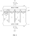
図2は、4:1行多重化(すなわち、4行に1行が、書き込みの間、共用の差動書き込みドライバー34’によって駆動され、その一方で、4行に1行が、読み取りの間、共用の差動感知増幅器40’に連結される)を例示するダイヤグラムである。図2に示されるように、各行は、1対のビットライン82−1および82−2に連結された複数のメモリポートを含み得る。例えば、メモリセル100は、1対の交差連結されたインバータ102および104から形成された双安定要素を含み得る。インバータ104は、セル100に対して、第1のデータストレージノードとして機能する出力を有し得、その一方で、インバータ102は、セル100に対して第2のデータストレージノードとして機能する出力を有し得る。第1のアクセストランジスタ106は、第1のデータストレージノードと第1のビットライン82−1との間に連結され得、その一方で、第2のアクセストランジスタ108は、第2のデータストレージノードと第1のビットライン82−2との間に連結され得る。アクセストランジスタ106および108(ときには、アドレストランジスタと呼ばれる)は、ワードライン80をわたって提供されたワードライン信号WLによって制御され得る。この例において、信号WLは、メモリセル100のうちの1列を選択するようにアサートされ得、隣接するセルの4つに1つからの外側の1つは、データローディング動作の間に関連付けられた書き込みドライバー34’、またはデータ感知する動作の間に関連付けられた感知増幅器に連結され得る。
FIG. 2 illustrates 4: 1 row multiplexing (ie, one row in four rows is driven by a shared differential write driver 34 'during writing, while one row in four rows during reading). , Coupled to a shared differential sense amplifier 40 '). As shown in FIG. 2, each row may include a plurality of memory ports coupled to a pair of bit lines 82-1 and 82-2. For example,
図2のメモリセルは、単なる例示に過ぎず、本発明の範囲を限定するように意図されていない。所望なら、メモリセル10は、単一端部の単一ポートメモリセルであり得、2つより多い交差連結された反転回路を含み得、または任意の適切な単一ポートメモリ構成を用いて実装され得る。 The memory cell of FIG. 2 is merely exemplary and is not intended to limit the scope of the present invention. If desired, memory cell 10 can be a single-ended single-port memory cell, can include more than two cross-coupled inverting circuits, or can be implemented using any suitable single-port memory configuration. obtain.
図3は、要求生成器60(すなわち、要求生成器60−Aまたは60−B)の回路ダイヤグラムである。図3に示されるように、要求生成器60は、書き込み要求信号WREQが受信され得る第1の入力と、読み取り要求信号RREQが受信され得る第2の入力と、信号ENDが受信され得る第3の出力とを有し得る。要求生成器60は、生成器60に対して第1および第2の入力として機能する第1および第2の入力を有する(すなわち、生成器110の第1の入力がWREQを受信し得、その一方で、生成器110の第2の入力がRREQを受信し得る)論理ORゲート110を含み得る。論理ゲート110は、1ショットパルス生成器112に連結されている出力を有し得る。1ショットパルス生成器112は、信号WREQおよび/またはRREQの立ち上りエッジを検出することに応じて所与のパルス幅を有するパルスを生成するように構成され得る。
FIG. 3 is a circuit diagram of request generator 60 (ie, request generator 60-A or 60-B). As shown in FIG. 3, the
生成器112によって生成されたパルスは、インバータ114を介してラッチング回路62の第1の入力に与えられ得る。回路62は、(例として)交差連結された論理NANDゲート116および118を含む設定−再設定(SR)ラッチであり得る。所与のパルス幅は、ラッチ62の状態を設定または再設定するように十分の時間を提供するために、十分に広くあり得る。ラッチング回路62は、インバータ119を介して信号ENDを受信するように構成された第2の入力と、信号REQが提供される出力とを有し得る。1ショットパルス生成器112がSRラッチ62の「設定」入力に連結されているので、信号REQは、信号WERQおよび/またはRREQの立ち上りエッジを検出することに応じて高く上げられる(すなわち、ラッチ62は、高い状態に置かれる)。信号ENDがSRラッチ62の「再設定」入力にルーティングされるので、ラッチ62は、アサートされた信号ENDを検出することに応じて低い状態に置かれ得る(すなわち、信号REQは、強制的に低くされる)。
The pulse generated by the generator 112 may be provided to the first input of the latching
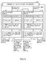
仲裁回路64は、同期モードまたは非同期モードで動作可能であり得る。同期モードにおいて、複数のポートからの要求は、単一クロックソースを用いて制御され得る。結果として、複数のポートからのメモリアクセス要求は、単一クロック信号の立ち上りエッジにおいて同時に到達し得る。同期モードの仲裁回路64は、例えば、複数のポートのうちのどれが図4の表に基づいて選択されるべきであるかを決定し得る。
2つのポートのうちの1つのみに未処理の要求があるシナリオにおいて、未処理の要求に関連付けられたポートは、処理のために選択され得る(例えば、列120を参照)。1つのポートが書き込み要求を受信し、およびもう1つのポートが読み取り要求を受信するシナリオにおいて、読み取り要求を受信するポートは、処理のために選択され得る(すなわち、列122に示されるように、仲裁回路64は、読み取りポートの優先度を実装するように構成され得る)。所望なら、仲裁回路64はまた、書き込みポート優先度を実装するように構成され得る(すなわち、書き込み要求を受信するポートは、処理のために選択され得る)。両方のポートが書き込み要求を受信し、または両方のポートが読み取り要求を受信するシナリオにおいて、列124に例示されるように、第2のポートBは、所与の優先度を有し得る(すなわち、ポートBでの要求は、ポートAでの要求の前に処理される)。所望なら、仲裁回路64はまた、両方のポートが同じタイプのメモリ要求を受信したときに、ポートAが優先であることを実装するように構成され得る(すなわち、ポートAおよびBの両方が読み取り要求を受信する場合、またはポートAおよびBの両方が書き込み要求を受信する場合、ポートAでの要求は、ポートBでの要求の前に処理される)。
In a scenario where there is an outstanding request on only one of the two ports, the port associated with the outstanding request may be selected for processing (see, eg, column 120). In a scenario where one port receives a write request and another port receives a read request, the port that receives the read request can be selected for processing (ie, as shown in
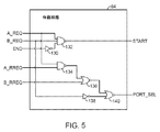
図5は、図4の表に関連して説明されるポート選択能力を提供するように構成された仲裁回路64の回路ダイヤグラムである。図5に示されるように、仲裁回路64は、論理NANDゲート132および134、並びに論理NORゲート136および140を含み得る。論理NANDゲート132は、要求生成器60−Aから信号A_REQを受信する第1の入力と、要求生成器60−Bから信号B_REQを受信する第2の入力と、インバータ130を介して制御回路30から信号ENDを受信する第3の入力とを有し得る。論理NANDゲート134は、信号A_REQを受信する第1の入力と、データレジスタおよび論理回路網72から信号A_RREQを受信する第2の入力と、出力とを有し得る。論理NORゲート136は、ゲート134の出力に連結されている第1の入力と、データレジスタおよび論理回路網72から信号B_RREQを受信する第2の入力と、出力とを有し得る。論理NORゲート140は、ゲート136の出力に連結されている第1の入力と、インバータ138を介して要求生成器60−Bから信号B_REQを受信する第2の入力と、信号PORT_SELが生成される出力とを有し得る。図5の例示的な回路ダイヤグラムは、単なる例示に過ぎず、本発明の範囲を限定するように機能しない。仲裁回路64は、所望のポート選択能力を提供するように構成された任意の適切な配列を用いて形成され得る。
FIG. 5 is a circuit diagram of an
図6は、同期モードにおいてメモリ回路網を動作させることにかかわる代表的なステップのフローチャートである。ステップ150において、仲裁回路64は、未処理の要求の存在をチェックし得る。少なくとも1つの未処理の要求が検出される場合に、選択されたポートに関連付けられた要求が満たされる(すなわち、要求が、図4に関連して説明されたタイプの論理表に基づいて選択されたポートに関連付けられる)。
FIG. 6 is a flowchart of representative steps involved in operating the memory circuitry in the synchronous mode. In
選択された要求を満たすことにおいて、仲裁回路64は、メモリアレイ22のアクセスを始動させるように制御回路30に指示するために、信号STARTをアサートし得る(ステップ154)。ステップ156において、信号PORT_SELは、仲裁回路64の論理に基づいて所望の値に設定され得る。ステップ158は、選択されたポートに関連付けられた読み取りまたは書き込み動作は、所望のメモリアドレスにおいて実行され得る。
In satisfying the selected request,
メモリアクセスが完了した際に、制御回路30は、現在の要求の完了を信号で送るために、選択されたポートに関連付けられた要求生成器を消去するように信号ENDを高くパルス化し得る(ステップ160)。パス162に示されるように、処理は、連続的な要求を処理するために、ステップ150に戻るようにループし得る。このときに、選択されていないポートに関連付けられた以前に未処理の要求(すなわち、選択されたポートに関連付けられた要求と平行して受信された要求)は、(存在する場合)、選択されたポートからの別の要求を処理する前に処理され得る。未処理の要求が存在しない場合に、仲裁回路64は、新しく到着するメモリ要求を待ち、かつその入力を監視し得る(ステップ150)。
When the memory access is complete, control circuit 30 may pulse signal END high to clear the request generator associated with the selected port in order to signal completion of the current request (step 160). As shown in
本発明の別の実施形態において、仲裁回路64は、非同期モードで(例えば、複数のポートからの要求が異なる位相および/または周波数のクロックを用いて制御されるモードにおいて)動作するように構成され得る。非同期デュアルポート動作において、異なるメモリポートからの要求は、しばしば、異なる時間に到達し得る。結果として、仲裁回路64は、第1の到達するメモリ要求が回路64によって受信されるとすぐに処理されることと、第1の到達メモリ要求が満たされたときに第2の(後に)到達するメモリ要求が処理されることとを行うように構成され得る。
In another embodiment of the present invention, the
図7は、非同期モードで動作可能な仲裁回路64の1つの適切な配列の例示的な回路ダイヤグラムである。図7に示されるように、仲裁回路64は、それぞれ、複数の入力および1つの出力を有する論理NANDゲート172、174、176、178、および180を含み得る。論理NANDゲート176は、要求生成器60−Aから信号A_REQを受信する第1の入力と、ゲート172の出力に連結されている第2の入力と、ゲート178の出力に連結されている第3の入力とを有し得、その出力において信号nA_GRANTを生成し得る。論理NANDゲート178は、要求生成器60−Bから信号B_REQを受信する第1の入力と、ゲート174の出力に連結されている第2の入力と、ゲート176の出力に連結されている第3の入力とを有し得、その出力において信号nB_GRANTを生成し得る。信号nA_GRANTは、生成器60−Aからの要求が選択される場合に強制的に低くされ得、その一方で、信号nB_GRANTは、生成器60−Bからの要求が選択される場合に強制的に低くされ得る。
FIG. 7 is an exemplary circuit diagram of one suitable arrangement of
仲裁回路64はまた、ゲート178の出力に連結された入力と、信号PORT_SELが提供される出力とを有するインバータ182を含み得る。論理NANDゲート180は、ゲート176の出力に連結された第1の入力と、ゲート178の出力に連結された第2の入力とを有し得、その出力において信号STARTを生成し得る。論理NANDゲート172は、インバータ182の出力に連結された第1の入力と、制御回路30から信号ENDを受信する第2の入力とを有し得、その一方で、論理NANDゲート174は、別のインバータ170を介してインバータ182の出力に連結されている第1の入力と、信号ENDを受信する第2の入力とを有し得る。
このように交差連結されたNANDゲート176および178は、仲裁回路64に対してラッチングおよびゲーティング能力を提供するように機能し得る。例えば、ゲート176および178は、信号nA_GRANTおよびnB_GRANTのうちの1つのみをアサートし、信号ENDの立ち上りエッジが検出される場合にのみPORT_SELをトグルする。図7の例示的な回路ダイヤグラムは、単なる例示に過ぎず、本発明の範囲を限定するように機能しない。
NAND gates 176 and 178 thus cross-coupled may function to provide latching and gating capabilities for
図8は、非同期モードで図1のメモリ回路網を動作させるための例示的なステップのフローチャートである。ステップ200において、仲裁回路64は、要求生成器60−A(ポートA)および60−B(ポートB)から要求を待ち得る。ポートAでの要求が、ポートBでの要求を検出する前に検出される場合に、ポートAからの要求が満たされ得る(ステップ202)。ポートBでの要求が、ポートAでの要求を検出する前に検出される場合に、ポートBからの要求が満たされ得る(ステップ216)。
FIG. 8 is a flowchart of exemplary steps for operating the memory circuitry of FIG. 1 in asynchronous mode. In
ステップ202において、信号STARTが、高く上げられ得、信号PORT_SELが、「0」に設定され得、所望の読み取り/書き込み動作が、特定のアドレス位置において実行され得る。ステップ210において、信号ENDは、要求生成器60−Aを消去し、および現在のメモリアクセスの完了を表すために信号STARTを低くするように高くパルス化され得る。未処理の要求がない場合には、パス212によって示されるように、処理は、ステップ200に戻るようにループされ得る。ポートBにおいて未処理の要求(すなわち、ステップ202が実行されている間に受信されている未処理の要求)が検出される場合には、パス214に示されるように、処理は、ステップ216に戻るようにループされ得る。
In
ステップ216において、ポートBからの要求が満たされ得る。例えば、信号STARTが、高く上げられ得、信号PORT_SELが、「1」に設定され得、所望の読み取り/書き込み動作が、特定のアドレス位置において実行され得る。ステップ224において、信号ENDは、要求生成器60−Bを消去し、および現在のメモリアクセスの完了を表すために信号STARTを低くするように高くパルス化され得る。未処理の要求がない場合には、パス226によって示されるように、処理は、ステップ200に戻るようにループされ得る。ポートAにおいて未処理の要求(すなわち、ステップ216が実行されている間に受信されている未処理の要求)が検出される場合には、パス228に示されるように、処理は、ステップ202に戻るようにループされ得る。
In
概して、ポートAおよびBからのメモリ要求が同時に到達するような場合に、2つの要求のうちのランダムの1つが、処理のために選択される。ポートAおよびBからの同時に到達するメモリ要求が満たされる順番に関わらず、仲裁回路64は、両方の要求されたメモリが確実に実行されるようにする。
In general, if memory requests from ports A and B arrive at the same time, a random one of the two requests is selected for processing. Regardless of the order in which simultaneously arriving memory requests from ports A and B are satisfied,
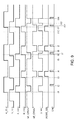
図9は、非同期モードにおける仲裁回路64の動作を示すタイミングダイヤグラムである。図9に示されるように、ポートAクロック信号A_CLKおよびポートBクロック信号B_CLKは、異なるクロック周波数および位相を有し得る。時間t1において、信号A_REQが高く上げられ、その一方で、B_REQは低いままである(すなわち、ポートAからの単一の要求が受信される)。A_REQの立ち上りに応じて、信号STARTが強制的に高くされ得、信号nA_GRANTが強制的に低くされ得る。時間t2において、信号ENDは、ポートAの要求の完了を表すために(生成器60−A内のラッチ62を消去するために)一時的に高くパルス化され得、A_REQおよびSTARTが強制的に低くさせられ、nA_GRANTが強制的に高くさせられる。
FIG. 9 is a timing diagram showing the operation of the
時間t3において、信号B_REQが高く上げられ、その一方で、A_REQは低いままである(すなわち、ポートBからの単一の要求が受信される)。B_REQの立ち上りに応じて、信号PORT_SELが強制的に高くされ得、信号STARTが強制的に高くされ得、信号nB_GRANTが強制的に低くされ得る。時間t4において、信号ENDは、ポートBの要求の完了を表すために(生成器60−B内のラッチ62を消去するために)一時的に高くパルス化され得、B_REQ、START、およびPORT_SELが強制的に低くさせられ、nB_GRANTが強制的に高くさせられる。それ故に、時間t1〜t4は、仲裁回路64は、2つの異なるポートから第1および第2の要求を受信し、第1の要求が満たされた後に第2の要求が受信されるシナリオを示す。
At time t3, signal B_REQ is raised high, while A_REQ remains low (ie, a single request from port B is received). In response to the rising edge of B_REQ, the signal PORT_SEL can be forced high, the signal START can be forced high, and the signal nB_GRANT can be forced low. At time t4, the signal END can be temporarily pulsed high (in order to clear the
時間t5からt9までに例示されるように、仲裁回路64は、ポートAからのメモリ要求を処理している間に、ポートBからメモリ要求を受信することも可能である。時間t5において、信号A_REQが高く上げられ、その一方で、B_REQは低いままである。A_REQの立ち上りに応じて、信号STARTが強制的に高くされ得、信号nA_GRANTが強制的に低くされ得る。時間t6において、信号B_REQが高く上げられ、その一方で、A_REQは依然高い(すなわち、ポートAに関連付けられたアクセスが完了する前に、要求がポートBにおいて受信された)。ポートAからの要求が未だ、完了されていないので、B_REQにおけるこの変化は、制御信号(すなわち、信号nA_GRANT、nB_GRANT、START、PORT_SEL、およびEND)に影響しない。
As illustrated from time t5 to t9,
時間t6の直後(時間t7)において、信号ENDは、ポートAの要求の完了を表すために高くパルス化され得、信号A_REQおよびSTARTが強制的に低くさせられ、nA_GRANTが強制的に高くさせられる。B_REQが依然高いので、仲裁回路64は、(時間t8において)信号PORT_SELを高く、信号STARTを高く、信号nB_GRANTを強制的に低くすることによってポートBからのこの未処理の要求を直ちに実行する。時間t9において、信号ENDは、ポートBの要求の完了を表すために一時的に高くパルス化され得、B_REQ、START、およびPORT_SELが強制的に低くさせられ、nB_GRANTが強制的に高くさせられる。それ故に、時間t5〜t9は、仲裁回路64は、2つの異なるポートから第1および第2の要求を受信し、第1の要求が満たされる前に第2の要求が受信されるシナリオを示す。
Immediately after time t6 (time t7), signal END can be pulsed high to indicate the completion of the request for port A, signals A_REQ and START are forced low, and nA_GRANT is forced high. . Since B_REQ is still high,
時間t10からt14までに例示されるように、仲裁回路64は、ポートBからのメモリ要求を処理している間に、ポートAからメモリ要求を受信することも可能である。時間t10において、信号B_REQが高く上げられ、その一方で、A_REQは低いままである。B_REQの立ち上りに応じて、信号PORT_SELが強制的に高くされ得、信号STARTが強制的に高くされ得、信号nB_GRANTが強制的に低くされ得る。時間t11において、信号A_REQが高く上げられ、その一方で、B_REQは依然高い(すなわち、ポートBに関連付けられたアクセスが完了する前に、要求がポートAにおいて受信された)。ポートBからの要求が未だ、完了されていないので、A_REQにおけるこの変化は、制御信号nA_GRANT、nB_GRANT、START、PORT_SEL、およびENDに影響しない。
As illustrated from time t10 to t14,
時間t11の直後(時間t12)において、信号ENDは、ポートBの要求の完了を表すために高くパルス化され得、信号B_REQ、START、およびPORT_SELが強制的に低くさせられ、nB_GRANTが強制的に高くさせられる。A_REQが依然高いので、仲裁回路64は、(時間t13において)信号STARTを高く、信号nA_GRANTを強制的に低くすることによってポートAからのこの未処理の要求を直ちに実行する。時間t14において、信号ENDは、ポートAの要求の完了を表すために一時的に高くパルス化され得、A_REQおよびSTARTが強制的に低くさせられ、nA_GRANTが強制的に高くさせられる。
Immediately after time t11 (time t12), signal END can be pulsed high to indicate the completion of the request for port B, signals B_REQ, START, and PORT_SEL are forced low and nB_GRANT is forced to Made high. Since A_REQ is still high,
図1〜9に関連して説明されたメモリ回路網のデュアル機能は、単なる例示に過ぎず、本発明の範囲を限定するように意図されていない。仲裁回路64は、ユーザーによって望まれるような同期モードまたは非同期モードで動作するように構成され得る(仲裁回路64は、現在のカスタム化可能な用途に依存して、同期モードと非同期モードとの間で切り替え得る)。所望なら、本明細書において説明された実施形態は、他のタイプのメモリセルに適用され得、同期および非同期モードで多重ポートメモリ動作をサポートするように構成され得る。
The dual functionality of the memory circuitry described in connection with FIGS. 1-9 is merely illustrative and is not intended to limit the scope of the invention.
(追加の実施形態)
(実施形態1)
第1および第2のポートを有するデュアルポートメモリであって、該デュアルポートメモリは、
単一ポートメモリ要素のアレイと、
該アレイに連結されており、かつ該アレイからデータを読み取り、該アレイにデータを書き込むように動作可能である制御回路と、
該第1のポートから第1のメモリアクセス要求を受信するように動作可能な第1の要求生成器と、
該第2のポートから第2のメモリアクセス要求を受信するように動作可能な第2の要求生成器と、
該制御回路、並びに該第1および第2の要求生成器に連結されている仲裁回路と
を含み、
該仲裁回路は、同期モードで動作可能であり、該同期モードにおいて、該第1および第2の要求生成器は、等しい周波数を有する少なくとも2つのクロック信号を用いて制御され、該少なくとも2つのクロック信号の各クロックサイクルの間に、該第1および第2のメモリアクセス要求のうちの1つのみを満たすために、該制御回路に指示するように動作可能である、デュアルポートメモリ。
(Additional embodiments)
(Embodiment 1)
A dual port memory having first and second ports, the dual port memory comprising:
An array of single-port memory elements;
A control circuit coupled to the array and operable to read data from and write data to the array;
A first request generator operable to receive a first memory access request from the first port;
A second request generator operable to receive a second memory access request from the second port;
An arbitration circuit coupled to the control circuit and the first and second request generators;
The arbitration circuit is operable in a synchronous mode in which the first and second request generators are controlled with at least two clock signals having equal frequencies and the at least two clocks A dual port memory operable to direct the control circuit to satisfy only one of the first and second memory access requests during each clock cycle of a signal.
(実施形態2)
上記第1および第2の要求生成器のうちの少なくとも1つは、パルス生成器およびラッチング回路を含み、該パルス生成器は、メモリアクセス要求を受信することに応じて、パルスを生成するように動作可能であり、該ラッチング回路は、該メモリアクセス要求が未だ実行されていない場合に、第1の論理値を格納するように動作可能であり、該メモリアクセス要求が上記制御回路を用いて実行された場合に、該第1の論理値とは異なる第2の論理値を格納するように動作可能である、実施形態1に記載のデュアルポートメモリ。
(Embodiment 2)
At least one of the first and second request generators includes a pulse generator and a latching circuit, wherein the pulse generator is configured to generate a pulse in response to receiving a memory access request. Operable and the latching circuit is operable to store a first logic value when the memory access request has not yet been executed, and the memory access request is executed using the control circuit. 2. The dual port memory of embodiment 1, wherein the dual port memory is operable to store a second logic value different from the first logic value when performed.
(実施形態3)
上記仲裁回路は、所定の論理表に基づく満足に対して、上記第1および第2のメモリアクセス要求のうちの1つのみを選択するように動作可能である、実施形態1に記載のデュアルポートメモリ。
(Embodiment 3)
2. The dual port of embodiment 1, wherein the arbitration circuit is operable to select only one of the first and second memory access requests for satisfaction based on a predetermined logic table. memory.
(実施形態4)
上記仲裁回路は、上記第1の要求生成器から第1の出力信号を受信するように動作可能である第1の入力と、上記第2の要求生成器から第2の出力信号を受信するように動作可能である第2の入力と、上記制御回路から制御信号を受信するように動作可能である第3の入力と、出力信号が提供される出力とを有する論理ゲートを含み、該出力信号は、該制御回路が上記アレイにアクセスしている間にアサートされる、実施形態1に記載のデュアルポートメモリ。
(Embodiment 4)
The arbitration circuit is configured to receive a first input operable to receive a first output signal from the first request generator and a second output signal from the second request generator. A logic gate having a second input operable to receive a control signal, a third input operable to receive a control signal from the control circuit, and an output provided with an output signal. 2. The dual port memory of embodiment 1, wherein the control circuit is asserted while accessing the array.
(実施形態5)
上記仲裁回路は、上記第2の要求生成器に連結されている第1の入力と、上記第1の要求生成器および該第2の要求生成器に連結されている第2の入力と、出力信号が提供される出力とを有する論理ゲートを含み、該出力信号は、上記第1のメモリアクセス要求を満たす場合に、第1の論理値を有し、上記第2のメモリアクセス要求を満たす場合に、該第1の論理値とは異なる第2の論理値を有する、実施形態1に記載のデュアルポートメモリ。
(Embodiment 5)
The arbitration circuit includes a first input coupled to the second request generator, a second input coupled to the first request generator and the second request generator, and an output. A logic gate having an output to which a signal is provided, the output signal having a first logic value when the first memory access request is satisfied and satisfying the second memory access request The dual port memory according to embodiment 1, further comprising a second logical value different from the first logical value.
(実施形態6)
上記仲裁回路は、非同期モードにおいてさらに動作可能であり、該非同期モードにおいて、上記第1および第2の要求生成器は、異なる周波数を有する少なくとも2つのクロック信号を用いて制御されている、実施形態1に記載のデュアルポートメモリ。
(Embodiment 6)
An embodiment wherein the arbitration circuit is further operable in an asynchronous mode, wherein the first and second request generators are controlled using at least two clock signals having different frequencies. 2. The dual port memory according to 1.
(実施形態7)
上記第1および第2の要求生成器のうちの少なくとも1つは、パルス生成器およびラッチング回路を含み、該パルス生成器は、メモリアクセス要求を受信することに応じて、パルスを生成するように動作可能であり、該ラッチング回路は、該メモリアクセス要求が未だ実行されていない場合に、第1の論理値を格納するように動作可能であり、該メモリアクセス要求が上記制御回路を用いて実行された場合に、該第1の論理値とは異なる第2の論理値を格納するように動作可能である、実施形態6に記載のデュアルポートメモリ。
(Embodiment 7)
At least one of the first and second request generators includes a pulse generator and a latching circuit, wherein the pulse generator is configured to generate a pulse in response to receiving a memory access request. Operable and the latching circuit is operable to store a first logic value when the memory access request has not yet been executed, and the memory access request is executed using the control circuit. 7. The dual port memory of embodiment 6, wherein the dual port memory is operable to store a second logic value that is different from the first logic value when the second logic value is stored.
(実施形態8)
上記仲裁回路は、上記同期モードで動作するとき、所定の論理表に基づく満足に対して、上記第1および第2のメモリアクセス要求のうちの1つのみを選択するように動作可能である、実施形態6に記載のデュアルポートメモリ。
(Embodiment 8)
The arbitration circuit is operable to select only one of the first and second memory access requests for satisfaction based on a predetermined logic table when operating in the synchronous mode; The dual port memory according to the sixth embodiment.
(実施形態9)
上記第1および第2のメモリアクセス要求は、異なる時間に到達し、上記仲裁回路は、上記非同期モードで動作するとき、満足に対して、該第1および第2のメモリアクセス要求のうちのより早く到達する1つを選択するように動作可能である、実施形態6に記載のデュアルポートメモリ。
(Embodiment 9)
The first and second memory access requests arrive at different times, and when the arbitration circuit operates in the asynchronous mode, the satisfaction of the first and second memory access requests Embodiment 7. The dual port memory of embodiment 6, operable to select one that arrives early.
(実施形態10)
上記仲裁回路は、上記第1および第2のメモリアクセス要求のうちの選択された1つを満たすように上記制御回路に指示するために、出力信号をアサートし、該選択されたメモリアクセス要求の満足に応じて該出力信号をデアサートするように動作可能である、実施形態6に記載のデュアルポートメモリ。
(Embodiment 10)
The arbitration circuit asserts an output signal to instruct the control circuit to satisfy a selected one of the first and second memory access requests, and the arbitration circuit 7. The dual port memory of embodiment 6 that is operable to deassert the output signal upon satisfaction.
(実施形態11)
第1および第2のポートを有するデュアルポートメモリであって、該デュアルポートメモリは、
単一ポートメモリ要素のアレイと、
該アレイに連結されており、かつ該アレイからデータを読み取り、該アレイにデータを書き込むように動作可能である制御回路と、
該第1のポートから第1のメモリアクセス要求を受信するように動作可能な第1の要求生成器と、
該第2のポートから第2のメモリアクセス要求を受信するように動作可能な第2の要求生成器と、
該制御回路、並びに該第1および第2の要求生成器に連結されている仲裁回路と
を含み、
該仲裁回路は、非同期モードで動作可能であり、該非同期モードにおいて、該第1および第2の要求生成器は、異なるそれぞれの周波数を有する2つの異なるクロック信号を用いて制御される、デュアルポートメモリ。
(Embodiment 11)
A dual port memory having first and second ports, the dual port memory comprising:
An array of single-port memory elements;
A control circuit coupled to the array and operable to read data from and write data to the array;
A first request generator operable to receive a first memory access request from the first port;
A second request generator operable to receive a second memory access request from the second port;
An arbitration circuit coupled to the control circuit and the first and second request generators;
The arbitration circuit is operable in an asynchronous mode, in which the first and second request generators are controlled using two different clock signals having different respective frequencies. memory.
(実施形態12)
上記第1および第2の要求生成器のうちの少なくとも1つは、パルス生成器およびラッチング回路を含み、該パルス生成器は、メモリアクセス要求を受信することに応じて、パルスを生成するように動作可能であり、該ラッチング回路は、該メモリアクセス要求が未だ実行されていない場合に、第1の論理値を格納するように動作可能であり、該メモリアクセス要求が上記制御回路を用いて実行された場合に、該第1の論理値とは異なる第2の論理値を格納するように動作可能である、実施形態11に記載のデュアルポートメモリ。
Embodiment 12
At least one of the first and second request generators includes a pulse generator and a latching circuit, wherein the pulse generator is configured to generate a pulse in response to receiving a memory access request. Operable and the latching circuit is operable to store a first logic value when the memory access request has not yet been executed, and the memory access request is executed using the control circuit. 12. The dual port memory of embodiment 11 that is operable to store a second logical value different from the first logical value when done.
(実施形態13)
上記第1および第2の要求生成器を制御する上記2つの異なるクロック信号は、異なるそれぞれの位相を有する、実施形態11に記載のデュアルポートメモリ。
(Embodiment 13)
12. The dual port memory of embodiment 11, wherein the two different clock signals controlling the first and second request generators have different respective phases.
(実施形態14)
上記第1および第2のメモリアクセス要求は、異なる時間に到達し、上記仲裁回路は、上記非同期モードで動作する間、満足に対して、該第1および第2のメモリアクセス要求のうちのより早く到達する1つを選択するように動作可能である、実施形態11に記載のデュアルポートメモリ。
(Embodiment 14)
The first and second memory access requests arrive at different times, and the arbitration circuit responds to satisfaction while operating in the asynchronous mode with respect to satisfaction of the first and second memory access requests. Embodiment 12. The dual port memory of embodiment 11 operable to select one that arrives early.
(実施形態15)
上記仲裁回路は、第1および第2の交差連結された論理ゲートを有するラッチング回路を含み、該第1の論理ゲートは、上記第1の要求生成器から第1の出力信号を受信するように動作可能であり、かつ第1の論理値を有する第1の制御信号を生成するように動作可能であり、該第2の論理ゲートは、上記第2の要求生成器から第2の出力信号を受信するように動作可能であり、かつ該第1の論理値とは異なる第2の論理値を有する第2の制御信号を生成するように動作可能である、実施形態11に記載のデュアルポートメモリ。
(Embodiment 15)
The arbitration circuit includes a latching circuit having first and second cross-coupled logic gates such that the first logic gate receives a first output signal from the first request generator. And operable to generate a first control signal having a first logic value, the second logic gate receiving a second output signal from the second request generator. 12. The dual port memory of embodiment 11, operable to receive and operable to generate a second control signal having a second logic value different from the first logic value. .
(実施形態16)
単一ポートメモリ要素のアレイと、第1および第2のポートとを含むデュアルポートメモリを使用するための方法であって、該方法は、
制御回路を用いて、該単一ポートメモリ要素のアレイにアクセスすることと、
第1の要求生成器を用いて、該第1のポートから第1のメモリアクセス要求を受信することと、
第2の要求生成器を用いて、該第2のポートから第2のメモリアクセス要求を受信することと、
仲裁回路を用いて、出力信号をアサートすることによって、該第1および第2のメモリアクセス要求のうちの選択された1つを満たすように該制御回路に指示することと
を含む、方法。
(Embodiment 16)
A method for using a dual port memory comprising an array of single port memory elements and first and second ports, the method comprising:
Accessing the array of single-port memory elements using a control circuit;
Receiving a first memory access request from the first port using a first request generator;
Receiving a second memory access request from the second port using a second request generator;
Using an arbitration circuit to instruct the control circuit to satisfy a selected one of the first and second memory access requests by asserting an output signal.
(実施形態17)
上記選択されたメモリアクセス要求の満足に応じて上記出力信号をデアサートすることをさらに含む、実施形態16に記載の方法。
(Embodiment 17)
17. The method of embodiment 16 further comprising deasserting the output signal in response to satisfaction of the selected memory access request.
(実施形態18)
同期モードで上記デュアルポートメモリを動作させることをさらに含み、該同期モードにおいて、上記第1および第2の要求生成器は、等しい周波数を有する少なくとも2つのクロック信号を用いて制御される、実施形態16に記載の方法。
(Embodiment 18)
An embodiment further comprising operating the dual port memory in a synchronous mode, wherein the first and second request generators are controlled using at least two clock signals having equal frequencies. 16. The method according to 16.
(実施形態19)
非同期モードで上記デュアルポートメモリを動作させることをさらに含み、該非同期モードにおいて、上記第1および第2の要求生成器は、異なる周波数を有する少なくとも2つのクロック信号を用いて制御される、実施形態16に記載の方法。
(Embodiment 19)
An embodiment further comprising operating the dual port memory in an asynchronous mode, wherein the first and second request generators are controlled using at least two clock signals having different frequencies. 16. The method according to 16.
(実施形態20)
同期モードで上記デュアルポートメモリを動作させることと、非同期モードで該デュアルポートメモリを動作させることをさらに含み、該同期モードにおいて、上記第1および第2の要求生成器は、等しい周波数を有する少なくとも2つのクロック信号を用いて制御され、該非同期モードにおいて、該第1および第2の要求生成器は、異なる周波数を有する少なくとも2つのクロック信号を用いて制御される、実施形態16に記載の方法。
(Embodiment 20)
Further comprising operating the dual port memory in a synchronous mode and operating the dual port memory in an asynchronous mode, wherein in the synchronous mode the first and second request generators have at least equal frequencies. Embodiment 17. The method of embodiment 16 wherein the method is controlled using two clock signals, and in the asynchronous mode, the first and second request generators are controlled using at least two clock signals having different frequencies. .
(実施形態21)
上記制御回路を用いて、上記選択されたメモリアクセス要求の満足に応じて制御信号をアサートすることと、
上記第1および第2の要求生成器を用いて該制御信号を受信することと
をさらに含む、実施形態16に記載の方法。
(Embodiment 21)
Using the control circuit to assert a control signal in response to satisfaction of the selected memory access request;
17. The method of embodiment 16, further comprising: receiving the control signal using the first and second request generators.
(実施形態22)
上記第1および第2の要求生成器のうちの少なくとも1つは、パルス生成器およびラッチング回路を含み、上記方法は、
該パルス生成器を用いて、メモリアクセス要求が該第1および第2の要求生成器のうちの該少なくとも1つに到達したことを検出することに応じてパルスを生成することと、
該ラッチング回路を用いて、該メモリアクセス要求が未だ満たされていない場合に、第1の論理値を格納し、該メモリアクセス要求が上記制御回路を用いて満たされた場合に、該第1の論理値とは異なる第2の論理値を格納することと
をさらに含む、実施形態16に記載の方法。
(Embodiment 22)
At least one of the first and second request generators includes a pulse generator and a latching circuit, the method comprising:
Using the pulse generator to generate a pulse in response to detecting that a memory access request has reached the at least one of the first and second request generators;
A first logic value is stored when the memory access request is not yet satisfied using the latching circuit, and the first logic value is stored when the memory access request is satisfied using the control circuit. 17. The method of embodiment 16, further comprising storing a second logical value that is different from the logical value.
上記の内容は、単なる本発明の原理の例示に過ぎず、さまざまな改変が、本発明の範囲および精神から逸脱することなしに、当業者によって加えられ得る。上記実施形態は、単独も任意の組み合わせでも実装され得る。 The foregoing is merely illustrative of the principles of this invention and various modifications can be made by those skilled in the art without departing from the scope and spirit of the invention. The above embodiments can be implemented alone or in any combination.
Claims (19)
単一ポートメモリ要素のアレイと、
該アレイに連結されており、かつ該アレイからデータを読み取り、該アレイにデータを書き込む制御回路と、
該第1のポートから第1のメモリアクセス要求を受信する第1の要求生成器と、
該第2のポートから第2のメモリアクセス要求を受信する第2の要求生成器と、
該制御回路、並びに該第1および第2の要求生成器に連結されている仲裁回路と
を含み、
該仲裁回路は、同期モードを有しており、該同期モードにおいて、該第1および第2の要求生成器は、第1および第2のクロック信号を用いて制御され、該第1および第2のクロック信号は、位相が整合しており、かつ、等しい周波数を有し、該仲裁回路は、読み取り優先および書き込み優先からなる群から選択される優先度に基づいて、該第1および第2のメモリアクセス要求のうちの所与の1つを満たすように、該制御回路に指示し、該仲裁回路は、該第1および第2のメモリアクセス要求のうちの該所与の1つを満たすように該制御回路に指示するために、出力信号をアサートし、該第1および第2のメモリアクセス要求のうちの該所与の1つの満足に応じて該出力信号をデアサートする、デュアルポートメモリ。 A dual port memory having first and second ports, the dual port memory comprising:
An array of single-port memory elements;
A control circuit coupled to and reading data from the array and writing data to the array;
A first request generator for receiving a first memory access request from the first port;
A second request generator for receiving a second memory access request from the second port;
An arbitration circuit coupled to the control circuit and the first and second request generators;
The arbitration circuit has a synchronous mode, in which the first and second request generators are controlled using first and second clock signals, and the first and second Of the first and second clock signals are in phase and equal in frequency, and the arbitration circuit determines whether the first and second are based on a priority selected from the group consisting of read priority and write priority. Instructing the control circuit to satisfy a given one of the memory access requests , the arbitration circuit satisfying the given one of the first and second memory access requests A dual port memory that asserts an output signal and deasserts the output signal in response to satisfaction of the given one of the first and second memory access requests to direct the control circuit to:
単一ポートメモリ要素のアレイと、
該アレイに連結されており、かつ該アレイからデータを読み取り、該アレイにデータを書き込む制御回路と、
該第1のポートから第1のメモリアクセス要求を受信する第1の要求生成器と、
該第2のポートから第2のメモリアクセス要求を受信する第2の要求生成器と、
該制御回路、並びに該第1および第2の要求生成器に連結されている仲裁回路と
を含み、
該仲裁回路は、非同期モードを有しており、該非同期モードにおいて、該第1および第2の要求生成器は、異なるそれぞれの周波数を有する2つの異なるクロック信号を用いて制御され、該2つの異なるクロック信号のうちの1つの周波数は、該2つの異なるクロック信号のうちの別の1つの整数倍ではなく、該仲裁回路は、同期モードも有しており、該仲裁回路は、所与の時間に、該同期モードおよび該非同期モードのうちの1つのみにおいて動作し、該仲裁回路は、該第1および第2のメモリアクセス要求のうちの所与の1つを満たすように該制御回路に指示するために、出力信号をアサートし、該第1および第2のメモリアクセス要求のうちの該所与の1つの満足に応じて該出力信号をデアサートする、デュアルポートメモリ。 A dual port memory having first and second ports, the dual port memory comprising:
An array of single-port memory elements;
A control circuit coupled to and reading data from the array and writing data to the array;
A first request generator for receiving a first memory access request from the first port;
A second request generator for receiving a second memory access request from the second port;
An arbitration circuit coupled to the control circuit and the first and second request generators;
The arbitration circuit has an asynchronous mode, in which the first and second request generators are controlled using two different clock signals having different respective frequencies, the two the frequency of one of the different clock signals, the two in another one integral multiple of the different clock signals rather than,該仲court circuit also has synchronous mode,該仲court circuit, given Operating in only one of the synchronous mode and the asynchronous mode, and the arbitration circuit controls the control to satisfy a given one of the first and second memory access requests. A dual port memory that asserts an output signal and deasserts the output signal in response to satisfaction of the given one of the first and second memory access requests to direct the circuit .
制御回路を用いて、該単一ポートメモリ要素のアレイにアクセスすることと、
第1の要求生成器を用いて、該第1のポートから第1のメモリアクセス要求を受信することと、
第2の要求生成器を用いて、該第2のポートから第2のメモリアクセス要求を受信することと、
仲裁回路を用いて、出力信号をアサートすることによって、該第1および第2のメモリアクセス要求のうちの選択された1つを満たすように該制御回路に指示することと、
該制御回路を用いて、該選択されたメモリアクセス要求の満足に応じて、制御信号をアサートすることと、
該第1および第2の要求生成器を用いて該制御信号を受信することと、
該制御回路が該制御信号をアサートすることに応じて、該仲裁回路を用いて、該出力信号をデアサートすることと
を含む、方法。 A method for using a dual port memory comprising an array of single port memory elements and first and second ports, the method comprising:
Accessing the array of single-port memory elements using a control circuit;
Receiving a first memory access request from the first port using a first request generator;
Receiving a second memory access request from the second port using a second request generator;
Using the arbitration circuit to instruct the control circuit to satisfy a selected one of the first and second memory access requests by asserting an output signal;
Using the control circuit to assert a control signal in response to satisfaction of the selected memory access request;
Receiving the control signal using the first and second request generators;
Deasserting the output signal using the arbitration circuit in response to the control circuit asserting the control signal.
該パルス生成器を用いて、メモリアクセス要求が該第1および第2の要求生成器のうちの該少なくとも1つに到達したことを検出することに応じてパルスを生成することと、
該ラッチング回路を用いて、該メモリアクセス要求が未だ満たされていない場合に、第1の論理値を格納し、該メモリアクセス要求が前記制御回路を用いて満たされた場合に、該第1の論理値とは異なる第2の論理値を格納することと
をさらに含む、請求項15に記載の方法。 At least one of the first and second request generators includes a pulse generator and a latching circuit, the method comprising:
Using the pulse generator to generate a pulse in response to detecting that a memory access request has reached the at least one of the first and second request generators;
A first logic value is stored when the memory access request is not yet satisfied using the latching circuit, and the first logic value is stored when the memory access request is satisfied using the control circuit. The method of claim 15 , further comprising storing a second logical value that is different from the logical value.
Applications Claiming Priority (2)
| Application Number | Priority Date | Filing Date | Title |
|---|---|---|---|
| US13/234,925 | 2011-09-16 | ||
| US13/234,925 US8867303B2 (en) | 2011-09-16 | 2011-09-16 | Memory arbitration circuitry |
Publications (3)
| Publication Number | Publication Date |
|---|---|
| JP2013065391A JP2013065391A (en) | 2013-04-11 |
| JP2013065391A5 JP2013065391A5 (en) | 2015-08-20 |
| JP6317876B2 true JP6317876B2 (en) | 2018-04-25 |
Family
ID=46799126
Family Applications (1)
| Application Number | Title | Priority Date | Filing Date |
|---|---|---|---|
| JP2012201000A Active JP6317876B2 (en) | 2011-09-16 | 2012-09-12 | Memory arbitration network |
Country Status (4)
| Country | Link |
|---|---|
| US (1) | US8867303B2 (en) |
| EP (1) | EP2571027A1 (en) |
| JP (1) | JP6317876B2 (en) |
| CN (1) | CN102999455B (en) |
Families Citing this family (7)
| Publication number | Priority date | Publication date | Assignee | Title |
|---|---|---|---|---|
| US9876501B2 (en) * | 2013-05-21 | 2018-01-23 | Mediatek Inc. | Switching power amplifier and method for controlling the switching power amplifier |
| US9183947B1 (en) * | 2014-04-16 | 2015-11-10 | Taiwan Semiconductor Manufacturing Company, Ltd. | Detecting write disturb in multi-port memories |
| CN107315703B (en) * | 2017-05-17 | 2020-08-25 | 天津大学 | Dual priority control type fair arbiter |
| US10622043B2 (en) | 2017-09-11 | 2020-04-14 | Qualcomm Incorporated | Multi-pump memory system access circuits for sequentially executing parallel memory operations |
| US10652912B2 (en) * | 2018-04-30 | 2020-05-12 | Microchip Technology Incorporated | Smart radio arbiter with conflict resolution based on timing predictability |
| US11031075B2 (en) * | 2019-05-08 | 2021-06-08 | Qualcomm Incorporated | High bandwidth register file circuit with high port counts for reduced bitline delay |
| US11264078B2 (en) * | 2020-02-04 | 2022-03-01 | Micron Technology, Inc. | Metastable resistant latch |
Family Cites Families (30)
| Publication number | Priority date | Publication date | Assignee | Title |
|---|---|---|---|---|
| US4796232A (en) | 1987-10-20 | 1989-01-03 | Contel Corporation | Dual port memory controller |
| US4937781A (en) | 1988-05-13 | 1990-06-26 | Dallas Semiconductor Corporation | Dual port ram with arbitration status register |
| US5047921A (en) | 1989-01-31 | 1991-09-10 | International Business Machines Corporation | Asynchronous microprocessor random access memory arbitration controller |
| US5001671A (en) * | 1989-06-27 | 1991-03-19 | Vitelic Corporation | Controller for dual ported memory |
| JPH0388196A (en) * | 1989-08-31 | 1991-04-12 | Sony Corp | Semiconductor memory |
| US5398211A (en) | 1993-10-14 | 1995-03-14 | Integrated Device Technology, Inc. | Structure and method for providing prioritized arbitration in a dual port memory |
| US5384737A (en) * | 1994-03-08 | 1995-01-24 | Motorola Inc. | Pipelined memory having synchronous and asynchronous operating modes |
| JPH0981449A (en) * | 1995-09-13 | 1997-03-28 | Fujitsu Ltd | Pseudo dual port memory |
| US5768211A (en) | 1996-07-31 | 1998-06-16 | Cypress Semiconductor Corporation | Multi-port arbitration for high performance width expansion |
| US5781480A (en) * | 1997-07-29 | 1998-07-14 | Motorola, Inc. | Pipelined dual port integrated circuit memory |
| US6078527A (en) * | 1997-07-29 | 2000-06-20 | Motorola, Inc. | Pipelined dual port integrated circuit memory |
| JP4153579B2 (en) * | 1998-01-22 | 2008-09-24 | 松下電器産業株式会社 | Memory access control device |
| TW451215B (en) * | 1998-06-23 | 2001-08-21 | Motorola Inc | Pipelined dual port integrated circuit memory |
| US5973985A (en) | 1998-08-11 | 1999-10-26 | Stmicroelectronics, Inc. | Dual port SRAM cell having pseudo ground line or pseudo power line |
| US6388939B1 (en) | 1999-09-30 | 2002-05-14 | Cypress Semiconductor Corp. | Dual port sram |
| US6118689A (en) | 1999-10-27 | 2000-09-12 | Kuo; James B. | Two-port 6T CMOS SRAM cell structure for low-voltage VLSI SRAM with single-bit-line simultaneous read-and-write access (SBLSRWA) capability |
| US6816955B1 (en) | 2000-09-29 | 2004-11-09 | Cypress Semiconductor Corp. | Logic for providing arbitration for synchronous dual-port memory |
| JP4997663B2 (en) * | 2000-12-27 | 2012-08-08 | 富士通セミコンダクター株式会社 | Multiport memory and control method thereof |
| US6751151B2 (en) | 2001-04-05 | 2004-06-15 | International Business Machines Corporation | Ultra high-speed DDP-SRAM cache |
| US6606275B2 (en) | 2001-08-23 | 2003-08-12 | Jeng-Jye Shau | High performance semiconductor memory devices |
| WO2003079194A1 (en) * | 2002-03-18 | 2003-09-25 | Matsushita Electric Industrial Co., Ltd. | Information processing apparatus |
| KR100560948B1 (en) | 2004-03-31 | 2006-03-14 | 매그나칩 반도체 유한회사 | 6 Transistor Dual Port SRAM Cell |
| US7349285B2 (en) * | 2005-02-02 | 2008-03-25 | Texas Instruments Incorporated | Dual port memory unit using a single port memory core |
| JP2006252656A (en) | 2005-03-10 | 2006-09-21 | Nec Electronics Corp | Multi-port memory device |
| JP4914034B2 (en) | 2005-06-28 | 2012-04-11 | セイコーエプソン株式会社 | Semiconductor integrated circuit |
| US7533222B2 (en) * | 2006-06-29 | 2009-05-12 | Mosys, Inc. | Dual-port SRAM memory using single-port memory cell |
| US7564738B2 (en) | 2006-08-11 | 2009-07-21 | Freescale Semiconductor, Inc. | Double-rate memory |
| JP4286295B2 (en) * | 2007-03-02 | 2009-06-24 | Okiセミコンダクタ株式会社 | Arbitration circuit |
| JP2010044821A (en) * | 2008-08-11 | 2010-02-25 | Hitachi Ulsi Systems Co Ltd | Semiconductor device and memory macro |
| US8514652B2 (en) * | 2011-03-02 | 2013-08-20 | Lsi Corporation | Multiple-port memory device comprising single-port memory device with supporting control circuitry |
-
2011
- 2011-09-16 US US13/234,925 patent/US8867303B2/en active Active
-
2012
- 2012-09-04 EP EP12182859A patent/EP2571027A1/en not_active Ceased
- 2012-09-07 CN CN201210331469.4A patent/CN102999455B/en active Active
- 2012-09-12 JP JP2012201000A patent/JP6317876B2/en active Active
Also Published As
| Publication number | Publication date |
|---|---|
| US20130073763A1 (en) | 2013-03-21 |
| CN102999455B (en) | 2017-10-27 |
| CN102999455A (en) | 2013-03-27 |
| EP2571027A1 (en) | 2013-03-20 |
| JP2013065391A (en) | 2013-04-11 |
| US8867303B2 (en) | 2014-10-21 |
Similar Documents
| Publication | Publication Date | Title |
|---|---|---|
| JP6317876B2 (en) | Memory arbitration network | |
| US6373779B1 (en) | Block RAM having multiple configurable write modes for use in a field programmable gate array | |
| US7903497B2 (en) | Multi-port SRAM implemented with single-port 6-transistor memory cells coupled to an input multiplexer and an output demultiplexer | |
| EP2263235B1 (en) | Address multiplexing in pseudo-dual port memory | |
| JP6293322B2 (en) | Time division multiplexed multiport memory. | |
| US9190127B2 (en) | Burst length control circuit | |
| US20080080297A1 (en) | Self-timed memory having common timing control circuit and method therefor | |
| JP5038657B2 (en) | Semiconductor integrated circuit device | |
| JP4456687B2 (en) | Random access memory and method of writing to and reading from the memory | |
| JP2005071454A (en) | Semiconductor memory device | |
| US9576630B2 (en) | Memory devices and methods having multiple address accesses in same cycle | |
| US9990985B1 (en) | Memory device with determined time window | |
| US9208856B2 (en) | Multiport memory with matching address control | |
| JP7376750B2 (en) | System and method for driving word lines using set-reset latches | |
| JP2022533622A (en) | Shiftable memory and methods of operating shiftable memory | |
| JP2009087534A (en) | Semiconductor storage device | |
| JP2010044821A (en) | Semiconductor device and memory macro | |
| KR100340067B1 (en) | Memory device having single port memory capable of reading and writing data at the same time | |
| US20190228821A1 (en) | Programmable High-Speed and Low-power Mode FPGA Memory with Configurable Floating Bitlines Scheme | |
| Shrivastava | Generic methodology to convert SPSRAM to PSEUDO SRAM with minimum design changes in SPSRAM architecture |
Legal Events
| Date | Code | Title | Description |
|---|---|---|---|
| A521 | Written amendment |
Free format text: JAPANESE INTERMEDIATE CODE: A523 Effective date: 20150701 |
|
| A621 | Written request for application examination |
Free format text: JAPANESE INTERMEDIATE CODE: A621 Effective date: 20150701 |
|
| A977 | Report on retrieval |
Free format text: JAPANESE INTERMEDIATE CODE: A971007 Effective date: 20160413 |
|
| A131 | Notification of reasons for refusal |
Free format text: JAPANESE INTERMEDIATE CODE: A131 Effective date: 20160418 |
|
| A521 | Written amendment |
Free format text: JAPANESE INTERMEDIATE CODE: A523 Effective date: 20160719 |
|
| A131 | Notification of reasons for refusal |
Free format text: JAPANESE INTERMEDIATE CODE: A131 Effective date: 20161222 |
|
| A601 | Written request for extension of time |
Free format text: JAPANESE INTERMEDIATE CODE: A601 Effective date: 20170321 |
|
| A521 | Written amendment |
Free format text: JAPANESE INTERMEDIATE CODE: A523 Effective date: 20170411 |
|
| A02 | Decision of refusal |
Free format text: JAPANESE INTERMEDIATE CODE: A02 Effective date: 20170815 |
|
| A521 | Written amendment |
Free format text: JAPANESE INTERMEDIATE CODE: A523 Effective date: 20171215 |
|
| A911 | Transfer of reconsideration by examiner before appeal (zenchi) |
Free format text: JAPANESE INTERMEDIATE CODE: A911 Effective date: 20171225 |
|
| TRDD | Decision of grant or rejection written | ||
| A01 | Written decision to grant a patent or to grant a registration (utility model) |
Free format text: JAPANESE INTERMEDIATE CODE: A01 Effective date: 20180305 |
|
| A61 | First payment of annual fees (during grant procedure) |
Free format text: JAPANESE INTERMEDIATE CODE: A61 Effective date: 20180402 |
|
| R150 | Certificate of patent or registration of utility model |
Ref document number: 6317876 Country of ref document: JP Free format text: JAPANESE INTERMEDIATE CODE: R150 |