JP6317104B2 - Biological electrode - Google Patents
Biological electrode Download PDFInfo
- Publication number
- JP6317104B2 JP6317104B2 JP2013269227A JP2013269227A JP6317104B2 JP 6317104 B2 JP6317104 B2 JP 6317104B2 JP 2013269227 A JP2013269227 A JP 2013269227A JP 2013269227 A JP2013269227 A JP 2013269227A JP 6317104 B2 JP6317104 B2 JP 6317104B2
- Authority
- JP
- Japan
- Prior art keywords
- electrode
- pattern
- section
- lead wire
- ground terminal
- Prior art date
- Legal status (The legal status is an assumption and is not a legal conclusion. Google has not performed a legal analysis and makes no representation as to the accuracy of the status listed.)
- Active
Links
- 239000010410 layer Substances 0.000 claims description 35
- 239000000463 material Substances 0.000 claims description 26
- 239000000853 adhesive Substances 0.000 claims description 17
- 230000001070 adhesive effect Effects 0.000 claims description 17
- WABPQHHGFIMREM-UHFFFAOYSA-N lead(0) Chemical compound [Pb] WABPQHHGFIMREM-UHFFFAOYSA-N 0.000 claims description 15
- BQCADISMDOOEFD-UHFFFAOYSA-N Silver Chemical compound [Ag] BQCADISMDOOEFD-UHFFFAOYSA-N 0.000 claims description 14
- 238000001514 detection method Methods 0.000 claims description 14
- 229910052709 silver Inorganic materials 0.000 claims description 14
- 239000004332 silver Substances 0.000 claims description 14
- 239000004020 conductor Substances 0.000 claims description 8
- 239000000758 substrate Substances 0.000 claims description 7
- 239000000126 substance Substances 0.000 claims description 5
- 239000002356 single layer Substances 0.000 claims description 3
- RYGMFSIKBFXOCR-UHFFFAOYSA-N Copper Chemical compound [Cu] RYGMFSIKBFXOCR-UHFFFAOYSA-N 0.000 claims description 2
- 229910052802 copper Inorganic materials 0.000 claims description 2
- 239000010949 copper Substances 0.000 claims description 2
- PCHJSUWPFVWCPO-UHFFFAOYSA-N gold Chemical compound [Au] PCHJSUWPFVWCPO-UHFFFAOYSA-N 0.000 claims description 2
- 229910052737 gold Inorganic materials 0.000 claims description 2
- 239000010931 gold Substances 0.000 claims description 2
- 229910052751 metal Inorganic materials 0.000 description 8
- 239000002184 metal Substances 0.000 description 8
- OKTJSMMVPCPJKN-UHFFFAOYSA-N Carbon Chemical compound [C] OKTJSMMVPCPJKN-UHFFFAOYSA-N 0.000 description 6
- 229910052799 carbon Inorganic materials 0.000 description 6
- 230000005611 electricity Effects 0.000 description 5
- 230000003068 static effect Effects 0.000 description 5
- 229910045601 alloy Inorganic materials 0.000 description 4
- 239000000956 alloy Substances 0.000 description 4
- 230000001965 increasing effect Effects 0.000 description 4
- 239000000203 mixture Substances 0.000 description 4
- 230000000694 effects Effects 0.000 description 3
- 229910021607 Silver chloride Inorganic materials 0.000 description 2
- 230000003247 decreasing effect Effects 0.000 description 2
- 239000006260 foam Substances 0.000 description 2
- 150000002739 metals Chemical class 0.000 description 2
- 238000000034 method Methods 0.000 description 2
- 229910052755 nonmetal Inorganic materials 0.000 description 2
- 239000011347 resin Substances 0.000 description 2
- 229920005989 resin Polymers 0.000 description 2
- HKZLPVFGJNLROG-UHFFFAOYSA-M silver monochloride Chemical compound [Cl-].[Ag+] HKZLPVFGJNLROG-UHFFFAOYSA-M 0.000 description 2
- 238000011144 upstream manufacturing Methods 0.000 description 2
- 230000037303 wrinkles Effects 0.000 description 2
- 229920002799 BoPET Polymers 0.000 description 1
- 208000010201 Exanthema Diseases 0.000 description 1
- 229910017060 Fe Cr Inorganic materials 0.000 description 1
- 229910002544 Fe-Cr Inorganic materials 0.000 description 1
- 229910001030 Iron–nickel alloy Inorganic materials 0.000 description 1
- 229910003286 Ni-Mn Inorganic materials 0.000 description 1
- 206010045453 Umbilical cord short Diseases 0.000 description 1
- 230000004075 alteration Effects 0.000 description 1
- 229910052782 aluminium Inorganic materials 0.000 description 1
- XAGFODPZIPBFFR-UHFFFAOYSA-N aluminium Chemical compound [Al] XAGFODPZIPBFFR-UHFFFAOYSA-N 0.000 description 1
- UPHIPHFJVNKLMR-UHFFFAOYSA-N chromium iron Chemical compound [Cr].[Fe] UPHIPHFJVNKLMR-UHFFFAOYSA-N 0.000 description 1
- 239000011248 coating agent Substances 0.000 description 1
- 238000000576 coating method Methods 0.000 description 1
- 238000005260 corrosion Methods 0.000 description 1
- 230000007797 corrosion Effects 0.000 description 1
- 238000003745 diagnosis Methods 0.000 description 1
- 238000010586 diagram Methods 0.000 description 1
- 201000005884 exanthem Diseases 0.000 description 1
- 230000006698 induction Effects 0.000 description 1
- 230000001939 inductive effect Effects 0.000 description 1
- 239000012212 insulator Substances 0.000 description 1
- 230000007774 longterm Effects 0.000 description 1
- 238000012423 maintenance Methods 0.000 description 1
- 238000005259 measurement Methods 0.000 description 1
- 229910021404 metallic carbon Inorganic materials 0.000 description 1
- 239000004745 nonwoven fabric Substances 0.000 description 1
- 230000003647 oxidation Effects 0.000 description 1
- 238000007254 oxidation reaction Methods 0.000 description 1
- 239000003973 paint Substances 0.000 description 1
- 235000011837 pasties Nutrition 0.000 description 1
- 230000002093 peripheral effect Effects 0.000 description 1
- 230000000644 propagated effect Effects 0.000 description 1
- 206010037844 rash Diseases 0.000 description 1
- 238000007789 sealing Methods 0.000 description 1
- 230000001629 suppression Effects 0.000 description 1
Images


Landscapes
- Measurement And Recording Of Electrical Phenomena And Electrical Characteristics Of The Living Body (AREA)
Description
本発明は主に生体電気信号取得用の電極(生体電極)に関し、特に、使い捨て型の生体電極に関する。 The present invention mainly relates to an electrode (bioelectrode) for obtaining a bioelectric signal, and more particularly, to a disposable bioelectrode.
従来、心電図を代表とする生体電気信号は、診断に有用な情報として広く用いられている。生体電気信号はその目的に応じて、安静時のみならず、運動中や日常生活中に取得することもある。例えば、ホルタ心電計による心電図取得は、日常生活中に長期間連続して生体電気信号を取得する代表的なものである。 Conventionally, bioelectric signals typified by an electrocardiogram have been widely used as information useful for diagnosis. Depending on the purpose, the bioelectric signal may be acquired not only at rest but also during exercise and daily life. For example, electrocardiogram acquisition using a Holter electrocardiograph is a typical example of acquiring a bioelectric signal continuously for a long time during daily life.
生体電気信号の取得には、体表面に装着する生体電極が必要である。そして、生体電極には、取得期間に渡って少ないノイズで安定した生体電気信号を取得することが求められる。そのため、生体電極には、取得する生体電気信号の種類や、取得環境、取得期間などに応じて様々な形態のものが存在する。 In order to acquire a bioelectric signal, a bioelectrode attached to the body surface is required. The bioelectrode is required to acquire a stable bioelectric signal with little noise over the acquisition period. Therefore, there are various types of bioelectrodes depending on the type of bioelectric signal to be acquired, the acquisition environment, the acquisition period, and the like.
長時間の使用が前提の生体電極は、衛生面やメンテナンスの手間を省くといった観点から、使い捨て(シングルユース)可能であることが望ましい。そのため、樹脂フィルムに配線パターンを印刷し、発泡シートのような絶縁物でサンドイッチした構成のような、低コストで製造可能な構成を有している(特許文献1)。 A bioelectrode premised on long-term use is desirably disposable (single use) from the viewpoint of saving hygiene and maintenance. Therefore, it has a configuration that can be manufactured at low cost, such as a configuration in which a wiring pattern is printed on a resin film and sandwiched with an insulator such as a foam sheet (Patent Document 1).
ホルタ心電計による生体電気信号取得の大半は、被検者が着衣状態かつ安静でない状態で行われるため、被検者の体動によって生体電極と着衣との間で絶えず摩擦が生じる。上述の通り、使い捨て型の生体電極は低コストで製造する必要があるため、再利用を前提とした生体電極で用いられるようなシールドを内蔵した同軸誘導コードを用いることはできない。また、主に樹脂系の素材を用いて形成されるため、摩擦による静電気で帯電しやすい。そのため、特許文献1記載の生体電極では、静電気によって生体電気信号に重畳するノイズを抑制するための、導電性物質からなるシールドパターン(シールド層)を上面および下面に設けている。 Since most of the bioelectric signal acquisition by the Holter electrocardiograph is performed while the subject is in a clothing state and not at rest, friction is constantly generated between the biological electrode and the clothing due to the body movement of the subject. As described above, since the disposable bioelectrode needs to be manufactured at a low cost, a coaxial induction cord with a built-in shield that is used in a bioelectrode premised on reuse cannot be used. Moreover, since it is mainly formed using a resin-based material, it is easily charged by static electricity due to friction. For this reason, the bioelectrode described in Patent Document 1 is provided with shield patterns (shield layers) made of a conductive material on the upper and lower surfaces for suppressing noise superimposed on the bioelectric signal due to static electricity.
従来、このようなシールドパターンは一般に、カーボンと銀とを含有する導電性塗料を塗布(印刷)することで形成されることが多いが、帯電防止(ノイズ抑制)が必ずしも十分でなく、さらなる改良が望まれていた。 Conventionally, such a shield pattern is generally formed by applying (printing) a conductive paint containing carbon and silver, but antistatic (noise suppression) is not always sufficient, and further improvement Was desired.
本発明は、このような従来技術の問題点に鑑みなされたものであり、耐ノイズ性に優れ、かつ低コストで製造可能な生体電極を提供することを目的とする。 The present invention has been made in view of such problems of the prior art, and an object thereof is to provide a biological electrode that is excellent in noise resistance and can be manufactured at low cost.
上述の目的は、生体に装着する電極パッドと、電極パッドに一端を固定され、平板状の基材に複数の層が形成された積層構造を有するリード線部と、を有する生体電極であって、リード線部が、接地端子に接続されるシールド層を有し、シールド層の第1の区間が単層構造を有し、第1の区間より接地端子に近い第2の区間が、第1の区間の構造に加え、接地端子に接続される導電細線パターンを有する多層構造を有することにより、シールド層の抵抗率が、第1の区間における抵抗率よりも、第2の区間における抵抗率の方が低くなるように制御されることを特徴とする生体電極によって達成される。 The above objects, an electrode pad to be attached to a living body, is secured at one end to the electrode pad, BIOLOGICAL electrodes that having a, a lead portion having a laminated structure in which a plurality of layers is formed on a flat substrate The lead wire portion has a shield layer connected to the ground terminal, the first section of the shield layer has a single layer structure, and the second section closer to the ground terminal than the first section is In addition to the structure of the first section, by having a multilayer structure having a conductive thin wire pattern connected to the ground terminal, the resistivity of the shield layer is higher in the second section than in the first section. This is achieved by a bioelectrode characterized in that the resistivity is controlled to be lower.
このような構成により、本発明によれば、耐ノイズ性に優れるとともに低コストで製造可能な生体電極を提供することができる。 With such a configuration, according to the present invention, it is possible to provide a biological electrode that has excellent noise resistance and can be manufactured at low cost.
以下、図面を参照して本発明の例示的な実施形態について詳細に説明する。
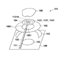
図1は、本発明の実施形態に係る生体電極のうち、一端を電極パッドに固定され、他端をコネクタに接続されるリード線部の基本的な構成例を示す分解斜視図である。電極パッドとリード線部とが一体に構成される使い捨て型の生体電極では、印刷や粘着材層を介した接着などよって平板状の基材に様々な機能を有する複数の層を形成した積層構造のリード線部を有する。本実施形態では、4つの電極を用いて2chの心電図の測定可能な生体電極に本発明を適用した例を説明する。しかし、本発明は心電図計測用の生体電極に限らず、他の生体電気信号を測定する電極にも適用可能である。また、電極の数にも特に制限は無く、1電極、3電極、5電極、7電極など、4電極以外の電極数の生体電極にも適用可能である。なお、1電極の場合、生体電気信号の測定時には他の1つ以上の電極と組み合わせて用いられる。他の1つ以上の電極は本実施形態で説明する構造を有するものであってもなくてもよい。
Hereinafter, exemplary embodiments of the present invention will be described in detail with reference to the drawings.
FIG. 1 is an exploded perspective view showing a basic configuration example of a lead wire portion in which one end is fixed to an electrode pad and the other end is connected to a connector, among biological electrodes according to an embodiment of the present invention. In a disposable bioelectrode in which the electrode pad and the lead wire part are integrated, a laminated structure in which a plurality of layers having various functions are formed on a flat base material by printing or adhesion via an adhesive material layer Lead wire part. In the present embodiment, an example in which the present invention is applied to a biological electrode capable of measuring a 2-ch electrocardiogram using four electrodes will be described. However, the present invention is not limited to a bioelectrode for electrocardiogram measurement, but can also be applied to electrodes for measuring other bioelectric signals. The number of electrodes is not particularly limited, and can be applied to biological electrodes having a number of electrodes other than four electrodes such as one electrode, three electrodes, five electrodes, and seven electrodes. In the case of one electrode, it is used in combination with one or more other electrodes when measuring a bioelectric signal. One or more other electrodes may or may not have the structure described in this embodiment.
図1に示す生体電極は、A〜Dの4つの電極を有する。各電極は基本的に共通の構成を有するが、電極Aは心電計(コネクタ)に近い位置に配置されている。一方、他の電極B〜Dについては、電極Aの外縁から、各電極に独立して設けられたコード部150を介して設けられている。なお、図1は生体電極の構成要素のうち、基材114に対して印刷によって設けられる層の構造を示している。図1に示す本実施形態の生体電極では、電極Cが共用電極である。
The bioelectrode shown in FIG. 1 has four electrodes A to D. Each electrode basically has a common configuration, but the electrode A is arranged at a position close to an electrocardiograph (connector). On the other hand, the other electrodes B to D are provided from the outer edge of the electrode A through a
なお、共用電極を用いない場合、2chの心電図波形を測定するための生体電極には5つの電極(1ch+/−,2ch+/−,不関電極)が必要である。5電極を用いる場合は、特許文献1に示されているように、個々の電極が独立したコード部を有する構成となる。 When the common electrode is not used, five electrodes (1ch +/−, 2ch +/−, indifferent electrode) are necessary for the bioelectrode for measuring the ECG waveform of 2ch. When five electrodes are used, as shown in Patent Document 1, each electrode has an independent cord portion.
平板状の基材114は例えばPETフィルムからなる。基材114の下面(電極装着時に体表面と対向する面)には、例えば印刷によりからなる電極パターン115が形成される。電極パターン115は先端部分が2層構造になっており、下層部分には円形の検出電極104と、検出電極104から手前に短いコード部1501が設けられている。また、後述する接続部121を設ける電極については、接続部121も下層に設けられる。下層部分は導電性粘着ゲル103と接する部分を含むため、変質しにくい塩化銀と銀の混合物から形成されている。一方、上層は銀から形成され、コード部150の先端部分1502は、下層の検出電極の中心からコード部1501と重複するように配置される。この重複部分は銀で形成されている上層の先端部分1502を塩化銀と銀の混合物で形成されている下層のコード部1501で保護するために設けられている。
The
電極パターン115の下面には、電極パターン115を絶縁するためのレジストパターン116がやはり印刷により設けられる。レジストパターン116の下面には、導電性物質からなる、静電気除去用の下シールドパターン117が印刷により設けられる。本実施形態では、下シールドパターン117はカーボンペーストで形成されている。下シールドパターン117のコード部150と、電極Aから至近端(コネクタ側)の下面、すなわち生体電極の最下面(生体表面に装着される面)には、不織布や発泡フォームといった、柔軟性を有する絶縁性シートが粘着材によって接着される。
A
基材114の上面(生体に装着されない面)には、上シールドパターン113が形成されている。本実施形態では、上シールドパターン113の抵抗率(または導電率)が少なくとも2段階に制御されていることを特徴とする。 An upper shield pattern 113 is formed on the upper surface of the base material 114 (the surface not attached to the living body). The present embodiment is characterized in that the resistivity (or conductivity) of the upper shield pattern 113 is controlled in at least two stages.
従来、上シールドパターン113はカーボンと銀がブレンドされた導電性ペーストで基材114の全面を覆うように形成される、すなわち上シールドパターン113の抵抗率又は導電率は全体を通じて一定であった。しかし、このようなシールドパターン(シールド層)では着衣との摩擦によって生じる静電気による電荷や外部から伝播するノイズに対するシールド効果は必ずしも十分ではなく、測定される生体電気信号に重畳するノイズのさらなる低減が求められていた。
Conventionally, the upper shield pattern 113 is formed to cover the entire surface of the
シールドの効果を高めるには、シールドの導電率を高め、ノイズの原因となる電荷を速やかに接地させれば良い。シールド層の形成にカーボンと銀がブレンドされた導電性ペーストを用いる場合であれば、カーボンの比率を下げて銀の比率を上げればよい。しかし、銀の比率を高めるとコストが大きく上昇し、使い捨てを前提とした生体電極には見合わなくなってしまう。発明者が検討したところ、カーボンと銀の比が1:1の導電性ペーストを用いた場合でも、耐ノイズ性能(シールド性能)は改良の余地があった。 In order to enhance the effect of the shield, it is only necessary to increase the conductivity of the shield and promptly ground the charge causing noise. If a conductive paste in which carbon and silver are blended is used for forming the shield layer, the ratio of silver may be increased by decreasing the ratio of carbon. However, when the silver ratio is increased, the cost is greatly increased, which makes it unsuitable for a bioelectrode that is assumed to be disposable. As a result of examination by the inventors, there was room for improvement in noise resistance performance (shield performance) even when a conductive paste having a carbon to silver ratio of 1: 1 was used.
ノイズの大半は、体表面と検出電極104とを電気的に接続するための導電性粘着ゲル103(図3参照)を通じて信号に重畳するが、静電気によるノイズはコード部150においても重畳する。従って、接地すべき総電荷量は、検出電極104を有する電極部1141から接地端子に向かって増加していく。そこで、上シールドパターン113の抵抗率を、接地端子に最も近い部分が最も低い抵抗率(または最も高い導電率)を有するように接地端子からの距離に応じて複数段階に制御することにより、耐ノイズ性能を向上できることを見出し、本発明に到達した。換言すれば、接地すべき総電荷量の増加に従って電荷の移動速度を向上させることで、電荷が経路上に滞留する時間を短縮させ、スムーズな耐電除去を実現するものである。
Most of the noise is superimposed on the signal through the conductive adhesive gel 103 (see FIG. 3) for electrically connecting the body surface and the
抵抗率または導電率の制御は、様々な方法により行うことが可能であるが、使い捨て型生体電極のように印刷を用いて配線やシールドパターンを形成する構成においては、シールドパターンを形成する物質の抵抗率または導電率を制御するか、層構成を制御することが現実的であろう。なお、以下では説明及び理解を容易にするため、抵抗率を制御するとの説明を行うが、抵抗率と導電率は逆数の関係にあり相互に変換可能であるため、導電率の制御としてもよいことはいうまでもない。 Control of resistivity or conductivity can be performed by various methods. However, in a configuration in which wiring or a shield pattern is formed using printing, such as a disposable bioelectrode, the substance that forms the shield pattern is controlled. It would be realistic to control the resistivity or conductivity or to control the layer configuration. In the following, for ease of explanation and understanding, the description will be made on controlling the resistivity. However, the resistivity and the conductivity are inversely related and can be converted to each other, and therefore the conductivity may be controlled. Needless to say.
図1には、上シールドパターン113を、共通の素材で生体電極全体に形成する全面パターン113Bに加え、抵抗値を低下させる区間には、導電性の高い物質で独立した細線状パターンを全面パターン113Bの下層に形成した構成により、2段階の抵抗率制御を実現した例を示している。 In FIG. 1, the upper shield pattern 113 is added to the entire surface of the living body electrode by using a common material, and a thin line pattern independent of a highly conductive material is formed on the entire surface pattern in a section where the resistance value is decreased. An example in which two-step resistivity control is realized by the configuration formed in the lower layer of 113B is shown.
導電細線パターン113Aは、導電率(電気伝導度)が高い物質から形成する。具体的には20℃における導電率が1.43×10⁵[S/m]以上(電気抵抗率が7×10-6[Ω・m]以下)の物質であることが好ましい。この条件を満たせば、非金属、金属、非金属と金属との混合物のいずれを用いてもよいが、金属を含有することが好ましい。金属の中でも、20℃における導電率が1.0×107[S/m]以上(電気抵抗率が10×10-8[Ω・m]以下)であるものが好ましく、20℃における導電率が2.5×107[S/m]以上(電気抵抗率が4×10-8[Ω・m]以下)であるものがさらに好ましい。この条件を満たす金属の例としては、単体では銀(6.4×107[S/m], 1.55×10⁻⁸[Ω・m])、銅(6.1×10⁷[S/m], 1.64×10⁻⁸[Ω・m])、アルミニウム(3.8×10⁷[S/m], 2.58×10⁻⁸[Ω・m])、金(3.0×10⁷[S/m], 3.28×10⁻⁸[Ω・m])などがある。
The thin
また、金属はFe-Cr系合金、Fe-Ni-Mn系合金やMo-Cr-Fe-Ni系合金など、合金であってもよい。また、非導電性の成分が含まれてもよい。具体的にどのような物質を用いるかは、細線パターンの形成方法や入手の容易性、コストなどを勘案して決定することができる。例えば印刷によってパターンを形成する場合、ペースト状の製品の入手性と導電率のバランスから銀や銀を含有する物質が好ましく用いることができる。 The metal may be an alloy such as an Fe—Cr alloy, an Fe—Ni—Mn alloy, or a Mo—Cr—Fe—Ni alloy. Further, a non-conductive component may be included. The specific substance to be used can be determined in consideration of the thin line pattern forming method, availability, cost, and the like. For example, when a pattern is formed by printing, silver or a substance containing silver can be preferably used from the balance between the availability of a pasty product and the conductivity.
導電細線パターン113Aが設けられた区間は、上層に設けられる全面パターン113Bを導通する電荷を、全面パターン113Bのみが設けられている区間よりも速やかに接地端子に向かって移送することができる。また、導電細線パターン113Aは、もともと、基材114の全面を隙間なく覆って単体でシールド機能を実現することを目的としておらず、高い導電性を有する高価な金属を用いる場合でも、少量で形成可能である。
In the section in which the conductive
なお、導電細線パターン113Aは、コード部150では1本の細線で構成されるが、コード部150より面積が大きく、かつ検出電極104が形成される電極部1141については、より効率よく電荷を捕集するため、二次元図形の外縁と、外縁内に存在し、外縁に接続される線状パターンからなるメッシュ状のパターン1131Aで形成することができる。ここで、メッシュの形状には特に制限は無いが、その外縁が、検出電極104の外縁もしくは、体表面と検出電極104とを電気的に接続するための導電性粘着ゲル103(図4参照)の外縁を包含するように形成することが好ましい。これは、ノイズの大半が導電性粘着ゲル103部分を通じて信号に重畳するためである。
The conductive
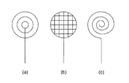
図1では、円の外縁と、円の外縁を6等分する点の2つを円の中心を通って接続する3つの直線パターンが導電性物質の細線で形成されたメッシュ形状を示しているが、図2(a)に示すように複数の同心円と、それらの外縁を接続する直線パターンを有する形状や、図2(b)に示すように規則的な格子状であってもよい。一方、図2(c)に示すようならせん状のパターンはここでいうメッシュ状のパターンには該当しない。なお、らせん状のパターンは外部からノイズが到来した際に誘導電流を生じるため好ましくない。メッシュ状のパターン1131Aは、基材114の電極部1141上の各位置から、メッシュ状のパターン1131Aを形成する細線までの最短距離にばらつきが少ない形状とすることが好ましい。換言すれば、外縁の内部に設けられるパターンは等間隔もしくは対称形状を有することが好ましい。
FIG. 1 shows a mesh shape in which three linear patterns connecting the outer edge of a circle and two points that divide the outer edge of the circle into six equal parts through the center of the circle are formed by thin lines of conductive material. However, a shape having a plurality of concentric circles as shown in FIG. 2 (a) and a linear pattern connecting the outer edges thereof, or a regular lattice shape as shown in FIG. 2 (b) may be used. On the other hand, the spiral pattern as shown in FIG. 2C does not correspond to the mesh pattern here. A spiral pattern is not preferable because an induced current is generated when noise comes from the outside. The
図3(a)は、図1に示した電極構造における上シールドパターン113が接地されるまでの経路を模式的に示している。図1の例では、基材114の下面側でのみコネクタと電気的に接続可能な構成を有するため、基材114の上面側に設けられる上シールドパターン113は、電極Bの上シールドパターン113と電極パターン115に設けられた接続部120,121と通じて電気的に接続されることで、接地されている。つまり、電極C,Dについての上シールドパターン113Bは電極A,B間の上シールドパターン113Bを経由して接地端子に接続されている。
FIG. 3A schematically shows a path until the upper shield pattern 113 in the electrode structure shown in FIG. 1 is grounded. In the example of FIG. 1, the upper shield pattern 113 provided on the upper surface side of the
そのため、本実施形態では、電極Aから電極Bへ至る経路では、(1)電極C,Dの導電性粘着ゲル103からのノイズ、(2)電極C,Dから電極Aに至るまでの経路でのノイズ、(3)電極Aの導電性粘着ゲル103からのノイズ、(4)コネクタ部品から電極Aまでの経路でのノイズ、に係る電荷を移送する必要がある。従って、複数の経路からのノイズに係る電荷が流入する位置(電極A)より下流(コネクタ接地端子側)の上シールドパターン113の抵抗率を、それより上流における抵抗率より低下させるように制御する。具体的には、電極Aから下流においては導電細線パターン113Aを設けて、上シールドパターン113を2層構造とする。
Therefore, in the present embodiment, the path from the electrode A to the electrode B is (1) noise from the conductive
導電細線パターン113Aの上に設けられる全面パターン113Bは、導電細線パターン113Aの上から基材114の表面全体を覆うように形成される。全面パターン113Bは導電性物質から形成されるが、導電細線パターン113Aを形成する物質よりも導電性が低い。また導電細線パターン113Aを酸化や腐食等の変質から保護する機能を持たせるため、全面パターン113Bも酸化や腐食をしにくい素材で形成することが好ましい。本実施形態ではこれらの条件を満たし、かつ印刷でパターンを形成可能な素材として、非金属であるカーボンペーストを用いて全面パターン113Bを形成しているが、金属の使用を含め、他の物質を用いてもよい。
The
上述の通り、導電細線パターン113Aは細線から形成されるいわば配線であるため、その面積は基材114よりずっと小さい。従って、導電性物質からなる全面パターン113Bは、導電細線パターン113Aから離れた位置に存在する電荷を導電細線パターン113Aまで速やかに移動させる経路を提供し、両者が設けられた区間では全面パターン113Bのみが設けられる区間よりも速やかな帯電除去が実現される。
As described above, since the conductive
なお、電極Bより下流では上述の(1)〜(4)に加え、(5)電極Aから電極Bに至るまでの経路でのノイズ、(6)電極Bの導電性粘着ゲル103からのノイズ、に係る電荷がさらに加わるため、接地電極Bに関する電極パターン115の抵抗率をさらに低下させてもよい。
In addition to the above (1) to (4), (5) noise in the path from the electrode A to the electrode B, and (6) noise from the conductive
なお、図1の例とは異なり、個々の電極が直接コネクタ接地端子に接続される形態(図3(b))では、電極部より下流の部分を電極部より低抵抗に構成すればよい。 Unlike the example of FIG. 1, in the form in which each electrode is directly connected to the connector ground terminal (FIG. 3B), the portion downstream from the electrode portion may be configured to have a lower resistance than the electrode portion.
なお、ここでは上シールドパターン113を二層構造として抵抗率の制御を行う例について説明したが、三層以上の多層構造としてもよいし、パターンの幅によって抵抗率を制御してもよい。上シールドパターン113を単層構造とする場合には、基材114の幅が下流に向かって広くなるように構成することができる。また、二層構造の場合でも、全面パターンでない層の幅を同様に制御することで抵抗率を制御できる。また、層の厚さを制御して抵抗率を制御してもよい。例えば、同一組成の導電性ペーストの塗布回数を接地端子に近い区間ほど増やすようにしてもよい。
Here, an example in which the resistivity is controlled by using the upper shield pattern 113 as a two-layer structure has been described, but a multilayer structure having three or more layers may be used, or the resistivity may be controlled by the width of the pattern. When the upper shield pattern 113 has a single layer structure, the width of the
なお、抵抗率を何段階に分けて制御するか、抵抗率をどこから変化させるか、ならびに具体的な抵抗率をどのように設定するかは、生体電極が使用される環境におけるノイズの特性などに応じて適宜定めることができる。ただし、接地すべき電荷が複数の経路から合流する位置より下流は、上流よりも抵抗を低下させるように制御することが好ましい。また、パターンの幅を制御する場合には、幅を徐々に拡げることで、滑らかに抵抗を低下させるように制御してもよい。 How many steps to control the resistivity, where to change the resistivity, and how to set the specific resistivity depends on the noise characteristics in the environment where the bioelectrode is used. It can be determined accordingly. However, it is preferable to perform control so that the resistance is lowered at the downstream side from the position where the charges to be grounded merge from the plurality of paths than at the upstream side. Further, when controlling the width of the pattern, the resistance may be smoothly reduced by gradually increasing the width.
図4は、本実施形態の生体電極における電極パッド101の構成を説明するための図である。電極パッドは生体表面に取り付けられる部分である。使い捨て型でない生体電極は、電極パッドとリード線(誘導コード)とが分離した構造を有するのが一般的であるが、使い捨て構造の場合は電極パッドとリード線とが一体化された構造を有する。
FIG. 4 is a diagram for explaining the configuration of the
図1に示したように、電極パターン115の先端部分に検出電極104が形成されている。電極パッド101のうち、導電性粘着ゲル103を体表面に固定するパッド基材106は、皮膚から発生する水分を発散させて皮膚に対する密着性を良好とし、かつ体動により生じる皮膚の皺などにも追従して変形可能とするため、柔軟性のある透湿防水フィルムで構成されている。パッド基材106として使用可能な透湿防水フィルムの厚さは、好ましくは20〜70μm、より好ましくは30〜60μm、特に好ましくは40〜60μm、最も好ましくは45〜55μmである。
As shown in FIG. 1, the
透湿防水フィルムが厚すぎると、皮膚からの水分を発散する効果が十分得られず、剥がれ易くなるほか、かぶれや蒸れなどの原因となり、装着感が悪化する。さらに、柔軟性(特に皮膚表面の皺に対する追従性)が低下するため、電極がごわごわして装着感が悪化するほか、剥がれやすくなる。さらに、柔軟性が低下することにより、生体電気信号にノイズが重畳しやすくなるという問題もある。 If the moisture permeable waterproof film is too thick, the effect of diffusing moisture from the skin cannot be obtained sufficiently, it becomes easy to peel off, and it causes rashes and stuffiness, which deteriorates the feeling of wearing. Furthermore, since flexibility (especially followability with respect to wrinkles on the surface of the skin) is reduced, the electrode is stiff and the wearing feeling is deteriorated, and it is easy to peel off. Furthermore, there is a problem that noise is easily superimposed on the bioelectric signal due to the decrease in flexibility.
パッド基材106の装着面には粘着剤が塗布されており、また、円弧状の第2のセパレータ102が装着面の外縁部に設けられている。第2のセパレータは剥離紙であり、電極パッド101全体のセパレータである第1のセパレータ109と対向する面は粘着性を有さない。従ってパッド基材106の装着面の第2のセパレータ102の存在する領域は第1のセパレータ109から容易に分離することが可能である。
An adhesive is applied to the mounting surface of the
パッド基材106の略中央部には電極に対応する穴1061が設けられている。図1における各電極A〜Dとその近傍はシール部材105によってパッド基材106に取り付けられるため、最上面および最下面には絶縁性シート111が設けられていない。
A
電極の下面には、導電性粘着ゲル103が設けられる。導電性粘着ゲル103は、電極の下面に塗布された導電性粘着剤により電極に取り付けられてもよいし、外周部分をパッド基材106の装着面に塗布される粘着剤によって固定され、電極とは直接接するようにされてもよい。
A conductive
シール部材105は、例えばパッド基材106と同じ透湿防水フィルムから構成される。シール部材105は、電極をパッド基材106に固定するために設けられる。
The
電極パッド101を装着する場合、まず第2のセパレータ102を用いて電極パッド101を第1のセパレータ109から分離する。そして、第2のセパレータ102で電極パッド101を支持しながら、装着部位に移動し、第2のセパレータの無い外縁部から体表面に貼り付ける。そして、第2のセパレータ102を剥がしながら、パッド基材106の全面を体表面に密着させる。
When mounting the
以上説明したように本実施形態によれば、電極パッドとリード線部とが一体的に構成される使い捨て型の生体電極におけるシールド層の抵抗率が、第1の区間より接地端子に近い第2の区間では第1の区間より低くなるように制御することにより、低コストで耐ノイズ性能を向上させることができる。 As described above, according to this embodiment, the resistivity of the shield layer in the disposable bioelectrode in which the electrode pad and the lead wire portion are integrally formed is closer to the ground terminal than in the first section. By controlling so that it becomes lower than the 1st area in this area, noise-proof performance can be improved at low cost.
Claims (8)
前記電極パッドに一端を固定され、平板状の基材に複数の層が形成された積層構造を有するリード線部と、を有する生体電極であって、
前記リード線部が、接地端子に接続されるシールド層を有し、
前記シールド層の第1の区間が単層構造を有し、前記第1の区間より前記接地端子に近い第2の区間が、前記第1の区間の構造に加え、前記接地端子に接続される導電細線パターンを有する多層構造を有することにより、前記シールド層の抵抗率が、前記第1の区間における抵抗率よりも、前記第2の区間における抵抗率の方が低くなるように制御されることを特徴とする生体電極。 An electrode pad attached to a living body;
The fixed at one end to the electrode pad, a live body electrode that Yusuke and the lead wire portion, a having a stacked structure in which a plurality of layers is formed on a flat substrate,
The lead wire portion has a shield layer connected to a ground terminal;
The first section of the shield layer has a single-layer structure, and the second section closer to the ground terminal than the first section is connected to the ground terminal in addition to the structure of the first section. by having a multi-layer structure having fine conductors pattern that the resistivity of the shield layer, than the resistivity of the first section, the direction of resistivity at the second section is controlled to be lower A bioelectrode characterized by.
前記二次元図形の外縁が、前記導電性粘着ゲルもしくは前記検出電極の外縁を包含するように形成されることを特徴とする請求項4に記載の生体電極。 The electrode pad is provided with a conductive adhesive gel for electrically connecting the detection electrode and the living body,
The bioelectrode according to claim 4 , wherein an outer edge of the two-dimensional figure is formed so as to include an outer edge of the conductive adhesive gel or the detection electrode.
前記電極パッドに一端を固定され、平板状の基材に複数の層が形成された積層構造を有するリード線部と、を有する生体電極であって、 A lead wire part having a laminated structure in which one end is fixed to the electrode pad and a plurality of layers are formed on a flat substrate,
前記リード線部の前記電極パッドに固定される部分が生体電気信号を検出する検出電極を含んだ電極部を形成し、 A portion fixed to the electrode pad of the lead wire portion forms an electrode portion including a detection electrode for detecting a bioelectric signal;
前記リード線部が、接地端子に接続されるシールド層を有し、 The lead wire portion has a shield layer connected to a ground terminal;
前記シールド層のうち、前記電極部に設けられる部分の抵抗値よりも、前記電極部より前記接地端子に近い部分に設けられる部分の抵抗値が低くなるように構成されることを特徴とする生体電極。 The living body characterized in that, in the shield layer, a resistance value of a portion provided in a portion closer to the ground terminal than the electrode portion is lower than a resistance value of a portion provided in the electrode portion. electrode.
Priority Applications (1)
| Application Number | Priority Date | Filing Date | Title |
|---|---|---|---|
| JP2013269227A JP6317104B2 (en) | 2013-12-26 | 2013-12-26 | Biological electrode |
Applications Claiming Priority (1)
| Application Number | Priority Date | Filing Date | Title |
|---|---|---|---|
| JP2013269227A JP6317104B2 (en) | 2013-12-26 | 2013-12-26 | Biological electrode |
Publications (3)
| Publication Number | Publication Date |
|---|---|
| JP2015123199A JP2015123199A (en) | 2015-07-06 |
| JP2015123199A5 JP2015123199A5 (en) | 2017-02-09 |
| JP6317104B2 true JP6317104B2 (en) | 2018-04-25 |
Family
ID=53534374
Family Applications (1)
| Application Number | Title | Priority Date | Filing Date |
|---|---|---|---|
| JP2013269227A Active JP6317104B2 (en) | 2013-12-26 | 2013-12-26 | Biological electrode |
Country Status (1)
| Country | Link |
|---|---|
| JP (1) | JP6317104B2 (en) |
Families Citing this family (2)
| Publication number | Priority date | Publication date | Assignee | Title |
|---|---|---|---|---|
| JP7033469B2 (en) * | 2017-04-28 | 2022-03-10 | 日東電工株式会社 | Biosensor |
| CN110545718B (en) * | 2017-04-28 | 2022-06-07 | 日东电工株式会社 | Biosensor with a sensor element |
Family Cites Families (8)
| Publication number | Priority date | Publication date | Assignee | Title |
|---|---|---|---|---|
| US4353372A (en) * | 1980-02-11 | 1982-10-12 | Bunker Ramo Corporation | Medical cable set and electrode therefor |
| US4442315A (en) * | 1980-11-17 | 1984-04-10 | Fukuda Denshi Kabushiki Kaisha | X-Ray transmissive electrode-shielded wire assembly and manufacture thereof |
| JPS5813182B2 (en) * | 1980-11-17 | 1983-03-12 | フクダ電子株式会社 | X-ray transparent electrode and lead wire |
| JP2553201Y2 (en) * | 1992-01-10 | 1997-11-05 | フクダ電子株式会社 | Plug structure used for nuclear magnetic resonance imaging |
| JP4588858B2 (en) * | 2000-10-20 | 2010-12-01 | フクダ電子株式会社 | Biological signal cable and biological signal processing apparatus |
| JP5165841B2 (en) * | 2005-08-09 | 2013-03-21 | フクダ電子株式会社 | Waterproof bioelectrode |
| JP2011182973A (en) * | 2010-03-09 | 2011-09-22 | Proassist:Kk | Brain wave collection controller |
| JP5727359B2 (en) * | 2011-12-27 | 2015-06-03 | 株式会社アイ・メデックス | Biological electrode and electrical connection structure between layers |
-
2013
- 2013-12-26 JP JP2013269227A patent/JP6317104B2/en active Active
Also Published As
| Publication number | Publication date |
|---|---|
| JP2015123199A (en) | 2015-07-06 |
Similar Documents
| Publication | Publication Date | Title |
|---|---|---|
| JP5670604B2 (en) | Biological electrode | |
| KR101538426B1 (en) | Electrode patch for measuring electrical signal from body and physiological signal measurement apparatus using it | |
| JP6695321B2 (en) | Biomedical electrode tool | |
| JP5727359B2 (en) | Biological electrode and electrical connection structure between layers | |
| JP6222546B2 (en) | Electrical impedance tomography measuring device | |
| JP6567800B2 (en) | Biological electrode | |
| JP5106885B2 (en) | Biological information measurement electrode | |
| JP6317104B2 (en) | Biological electrode | |
| CN110840448B (en) | Electrocardiogram electrode patch and preparation method thereof | |
| JP5836388B2 (en) | Biological electrode pad | |
| JP5888799B2 (en) | Biological electrode pad | |
| CN203776898U (en) | Flexible electrocardio-electrode | |
| JP7072446B2 (en) | Bioelectrode and its manufacturing method | |
| JP2004057704A (en) | Electrode device | |
| JP6677769B2 (en) | Biological electrode | |
| JP6027774B2 (en) | Biological information acquisition electrode | |
| JP2019068885A (en) | Bioelectrode and electric connection structure of interlayer | |
| CN205548558U (en) | Disposable noise proof, shielding electrode | |
| CN111132612B (en) | Device for sensing biological signals | |
| JP5984371B2 (en) | Biometric electrode | |
| FI131058B1 (en) | Interface structure for a bioelectrode | |
| WO2017157084A1 (en) | Disposable noise-canceling and shielding electrode |
Legal Events
| Date | Code | Title | Description |
|---|---|---|---|
| A521 | Request for written amendment filed |
Free format text: JAPANESE INTERMEDIATE CODE: A523 Effective date: 20161226 |
|
| A621 | Written request for application examination |
Free format text: JAPANESE INTERMEDIATE CODE: A621 Effective date: 20161226 |
|
| A977 | Report on retrieval |
Free format text: JAPANESE INTERMEDIATE CODE: A971007 Effective date: 20170830 |
|
| A131 | Notification of reasons for refusal |
Free format text: JAPANESE INTERMEDIATE CODE: A131 Effective date: 20170929 |
|
| A521 | Request for written amendment filed |
Free format text: JAPANESE INTERMEDIATE CODE: A523 Effective date: 20171128 |
|
| TRDD | Decision of grant or rejection written | ||
| A01 | Written decision to grant a patent or to grant a registration (utility model) |
Free format text: JAPANESE INTERMEDIATE CODE: A01 Effective date: 20180305 |
|
| A61 | First payment of annual fees (during grant procedure) |
Free format text: JAPANESE INTERMEDIATE CODE: A61 Effective date: 20180329 |
|
| R150 | Certificate of patent or registration of utility model |
Ref document number: 6317104 Country of ref document: JP Free format text: JAPANESE INTERMEDIATE CODE: R150 |
|
| R250 | Receipt of annual fees |
Free format text: JAPANESE INTERMEDIATE CODE: R250 |
|
| R250 | Receipt of annual fees |
Free format text: JAPANESE INTERMEDIATE CODE: R250 |