JP6306704B2 - Vertical power transistor device - Google Patents
Vertical power transistor device Download PDFInfo
- Publication number
- JP6306704B2 JP6306704B2 JP2016533399A JP2016533399A JP6306704B2 JP 6306704 B2 JP6306704 B2 JP 6306704B2 JP 2016533399 A JP2016533399 A JP 2016533399A JP 2016533399 A JP2016533399 A JP 2016533399A JP 6306704 B2 JP6306704 B2 JP 6306704B2
- Authority
- JP
- Japan
- Prior art keywords
- transistor device
- layer
- diffusion layer
- region
- power mosfet
- Prior art date
- Legal status (The legal status is an assumption and is not a legal conclusion. Google has not performed a legal analysis and makes no representation as to the accuracy of the status listed.)
- Active
Links
- 238000009792 diffusion process Methods 0.000 claims description 64
- 239000007943 implant Substances 0.000 claims description 33
- 239000000758 substrate Substances 0.000 claims description 28
- 230000005669 field effect Effects 0.000 claims description 9
- 230000007423 decrease Effects 0.000 claims description 7
- 229910044991 metal oxide Inorganic materials 0.000 claims description 4
- 150000004706 metal oxides Chemical class 0.000 claims description 4
- 239000004065 semiconductor Substances 0.000 claims description 4
- HBMJWWWQQXIZIP-UHFFFAOYSA-N silicon carbide Chemical compound [Si+]#[C-] HBMJWWWQQXIZIP-UHFFFAOYSA-N 0.000 claims description 3
- 229910010271 silicon carbide Inorganic materials 0.000 claims 2
- 238000000034 method Methods 0.000 description 19
- 230000008569 process Effects 0.000 description 18
- 230000005684 electric field Effects 0.000 description 13
- 238000004519 manufacturing process Methods 0.000 description 11
- 230000009471 action Effects 0.000 description 4
- 230000006872 improvement Effects 0.000 description 4
- 239000000463 material Substances 0.000 description 4
- 238000005468 ion implantation Methods 0.000 description 3
- 230000002829 reductive effect Effects 0.000 description 3
- IJGRMHOSHXDMSA-UHFFFAOYSA-N Atomic nitrogen Chemical compound N#N IJGRMHOSHXDMSA-UHFFFAOYSA-N 0.000 description 2
- PXHVJJICTQNCMI-UHFFFAOYSA-N Nickel Chemical compound [Ni] PXHVJJICTQNCMI-UHFFFAOYSA-N 0.000 description 2
- 229910052782 aluminium Inorganic materials 0.000 description 2
- XAGFODPZIPBFFR-UHFFFAOYSA-N aluminium Chemical compound [Al] XAGFODPZIPBFFR-UHFFFAOYSA-N 0.000 description 2
- 230000008859 change Effects 0.000 description 2
- 230000003247 decreasing effect Effects 0.000 description 2
- 230000000694 effects Effects 0.000 description 2
- 238000002513 implantation Methods 0.000 description 2
- 230000004048 modification Effects 0.000 description 2
- 238000012986 modification Methods 0.000 description 2
- 230000009467 reduction Effects 0.000 description 2
- 230000002441 reversible effect Effects 0.000 description 2
- JBRZTFJDHDCESZ-UHFFFAOYSA-N AsGa Chemical compound [As]#[Ga] JBRZTFJDHDCESZ-UHFFFAOYSA-N 0.000 description 1
- ZOXJGFHDIHLPTG-UHFFFAOYSA-N Boron Chemical compound [B] ZOXJGFHDIHLPTG-UHFFFAOYSA-N 0.000 description 1
- JMASRVWKEDWRBT-UHFFFAOYSA-N Gallium nitride Chemical compound [Ga]#N JMASRVWKEDWRBT-UHFFFAOYSA-N 0.000 description 1
- NPXOKRUENSOPAO-UHFFFAOYSA-N Raney nickel Chemical compound [Al].[Ni] NPXOKRUENSOPAO-UHFFFAOYSA-N 0.000 description 1
- RTAQQCXQSZGOHL-UHFFFAOYSA-N Titanium Chemical compound [Ti] RTAQQCXQSZGOHL-UHFFFAOYSA-N 0.000 description 1
- HZEWFHLRYVTOIW-UHFFFAOYSA-N [Ti].[Ni] Chemical compound [Ti].[Ni] HZEWFHLRYVTOIW-UHFFFAOYSA-N 0.000 description 1
- 238000013459 approach Methods 0.000 description 1
- 229910052796 boron Inorganic materials 0.000 description 1
- 238000005229 chemical vapour deposition Methods 0.000 description 1
- 238000010586 diagram Methods 0.000 description 1
- 238000005516 engineering process Methods 0.000 description 1
- 230000002452 interceptive effect Effects 0.000 description 1
- 230000000670 limiting effect Effects 0.000 description 1
- 229910052759 nickel Inorganic materials 0.000 description 1
- 229910052757 nitrogen Inorganic materials 0.000 description 1
- 230000007480 spreading Effects 0.000 description 1
- 238000003892 spreading Methods 0.000 description 1
- ISIJQEHRDSCQIU-UHFFFAOYSA-N tert-butyl 2,7-diazaspiro[4.5]decane-7-carboxylate Chemical compound C1N(C(=O)OC(C)(C)C)CCCC11CNCC1 ISIJQEHRDSCQIU-UHFFFAOYSA-N 0.000 description 1
- 239000010936 titanium Substances 0.000 description 1
- 229910052719 titanium Inorganic materials 0.000 description 1
Images


Classifications
-
- H—ELECTRICITY
- H01—ELECTRIC ELEMENTS
- H01L—SEMICONDUCTOR DEVICES NOT COVERED BY CLASS H10
- H01L29/00—Semiconductor devices adapted for rectifying, amplifying, oscillating or switching, or capacitors or resistors with at least one potential-jump barrier or surface barrier, e.g. PN junction depletion layer or carrier concentration layer; Details of semiconductor bodies or of electrodes thereof ; Multistep manufacturing processes therefor
- H01L29/66—Types of semiconductor device ; Multistep manufacturing processes therefor
- H01L29/68—Types of semiconductor device ; Multistep manufacturing processes therefor controllable by only the electric current supplied, or only the electric potential applied, to an electrode which does not carry the current to be rectified, amplified or switched
- H01L29/76—Unipolar devices, e.g. field effect transistors
- H01L29/772—Field effect transistors
- H01L29/78—Field effect transistors with field effect produced by an insulated gate
- H01L29/7801—DMOS transistors, i.e. MISFETs with a channel accommodating body or base region adjoining a drain drift region
- H01L29/7802—Vertical DMOS transistors, i.e. VDMOS transistors
-
- H—ELECTRICITY
- H01—ELECTRIC ELEMENTS
- H01L—SEMICONDUCTOR DEVICES NOT COVERED BY CLASS H10
- H01L29/00—Semiconductor devices adapted for rectifying, amplifying, oscillating or switching, or capacitors or resistors with at least one potential-jump barrier or surface barrier, e.g. PN junction depletion layer or carrier concentration layer; Details of semiconductor bodies or of electrodes thereof ; Multistep manufacturing processes therefor
- H01L29/02—Semiconductor bodies ; Multistep manufacturing processes therefor
- H01L29/06—Semiconductor bodies ; Multistep manufacturing processes therefor characterised by their shape; characterised by the shapes, relative sizes, or dispositions of the semiconductor regions ; characterised by the concentration or distribution of impurities within semiconductor regions
- H01L29/0684—Semiconductor bodies ; Multistep manufacturing processes therefor characterised by their shape; characterised by the shapes, relative sizes, or dispositions of the semiconductor regions ; characterised by the concentration or distribution of impurities within semiconductor regions characterised by the shape, relative sizes or dispositions of the semiconductor regions or junctions between the regions
-
- H—ELECTRICITY
- H01—ELECTRIC ELEMENTS
- H01L—SEMICONDUCTOR DEVICES NOT COVERED BY CLASS H10
- H01L29/00—Semiconductor devices adapted for rectifying, amplifying, oscillating or switching, or capacitors or resistors with at least one potential-jump barrier or surface barrier, e.g. PN junction depletion layer or carrier concentration layer; Details of semiconductor bodies or of electrodes thereof ; Multistep manufacturing processes therefor
- H01L29/02—Semiconductor bodies ; Multistep manufacturing processes therefor
- H01L29/06—Semiconductor bodies ; Multistep manufacturing processes therefor characterised by their shape; characterised by the shapes, relative sizes, or dispositions of the semiconductor regions ; characterised by the concentration or distribution of impurities within semiconductor regions
- H01L29/08—Semiconductor bodies ; Multistep manufacturing processes therefor characterised by their shape; characterised by the shapes, relative sizes, or dispositions of the semiconductor regions ; characterised by the concentration or distribution of impurities within semiconductor regions with semiconductor regions connected to an electrode carrying current to be rectified, amplified or switched and such electrode being part of a semiconductor device which comprises three or more electrodes
- H01L29/0843—Source or drain regions of field-effect devices
- H01L29/0847—Source or drain regions of field-effect devices of field-effect transistors with insulated gate
- H01L29/0852—Source or drain regions of field-effect devices of field-effect transistors with insulated gate of DMOS transistors
- H01L29/0856—Source regions
- H01L29/0865—Disposition
-
- H—ELECTRICITY
- H01—ELECTRIC ELEMENTS
- H01L—SEMICONDUCTOR DEVICES NOT COVERED BY CLASS H10
- H01L29/00—Semiconductor devices adapted for rectifying, amplifying, oscillating or switching, or capacitors or resistors with at least one potential-jump barrier or surface barrier, e.g. PN junction depletion layer or carrier concentration layer; Details of semiconductor bodies or of electrodes thereof ; Multistep manufacturing processes therefor
- H01L29/02—Semiconductor bodies ; Multistep manufacturing processes therefor
- H01L29/06—Semiconductor bodies ; Multistep manufacturing processes therefor characterised by their shape; characterised by the shapes, relative sizes, or dispositions of the semiconductor regions ; characterised by the concentration or distribution of impurities within semiconductor regions
- H01L29/08—Semiconductor bodies ; Multistep manufacturing processes therefor characterised by their shape; characterised by the shapes, relative sizes, or dispositions of the semiconductor regions ; characterised by the concentration or distribution of impurities within semiconductor regions with semiconductor regions connected to an electrode carrying current to be rectified, amplified or switched and such electrode being part of a semiconductor device which comprises three or more electrodes
- H01L29/0843—Source or drain regions of field-effect devices
- H01L29/0847—Source or drain regions of field-effect devices of field-effect transistors with insulated gate
- H01L29/0852—Source or drain regions of field-effect devices of field-effect transistors with insulated gate of DMOS transistors
- H01L29/0873—Drain regions
- H01L29/0878—Impurity concentration or distribution
-
- H—ELECTRICITY
- H01—ELECTRIC ELEMENTS
- H01L—SEMICONDUCTOR DEVICES NOT COVERED BY CLASS H10
- H01L29/00—Semiconductor devices adapted for rectifying, amplifying, oscillating or switching, or capacitors or resistors with at least one potential-jump barrier or surface barrier, e.g. PN junction depletion layer or carrier concentration layer; Details of semiconductor bodies or of electrodes thereof ; Multistep manufacturing processes therefor
- H01L29/02—Semiconductor bodies ; Multistep manufacturing processes therefor
- H01L29/06—Semiconductor bodies ; Multistep manufacturing processes therefor characterised by their shape; characterised by the shapes, relative sizes, or dispositions of the semiconductor regions ; characterised by the concentration or distribution of impurities within semiconductor regions
- H01L29/08—Semiconductor bodies ; Multistep manufacturing processes therefor characterised by their shape; characterised by the shapes, relative sizes, or dispositions of the semiconductor regions ; characterised by the concentration or distribution of impurities within semiconductor regions with semiconductor regions connected to an electrode carrying current to be rectified, amplified or switched and such electrode being part of a semiconductor device which comprises three or more electrodes
- H01L29/0843—Source or drain regions of field-effect devices
- H01L29/0847—Source or drain regions of field-effect devices of field-effect transistors with insulated gate
- H01L29/0852—Source or drain regions of field-effect devices of field-effect transistors with insulated gate of DMOS transistors
- H01L29/0873—Drain regions
- H01L29/0882—Disposition
-
- H—ELECTRICITY
- H01—ELECTRIC ELEMENTS
- H01L—SEMICONDUCTOR DEVICES NOT COVERED BY CLASS H10
- H01L29/00—Semiconductor devices adapted for rectifying, amplifying, oscillating or switching, or capacitors or resistors with at least one potential-jump barrier or surface barrier, e.g. PN junction depletion layer or carrier concentration layer; Details of semiconductor bodies or of electrodes thereof ; Multistep manufacturing processes therefor
- H01L29/02—Semiconductor bodies ; Multistep manufacturing processes therefor
- H01L29/06—Semiconductor bodies ; Multistep manufacturing processes therefor characterised by their shape; characterised by the shapes, relative sizes, or dispositions of the semiconductor regions ; characterised by the concentration or distribution of impurities within semiconductor regions
- H01L29/10—Semiconductor bodies ; Multistep manufacturing processes therefor characterised by their shape; characterised by the shapes, relative sizes, or dispositions of the semiconductor regions ; characterised by the concentration or distribution of impurities within semiconductor regions with semiconductor regions connected to an electrode not carrying current to be rectified, amplified or switched and such electrode being part of a semiconductor device which comprises three or more electrodes
- H01L29/1095—Body region, i.e. base region, of DMOS transistors or IGBTs
-
- H—ELECTRICITY
- H01—ELECTRIC ELEMENTS
- H01L—SEMICONDUCTOR DEVICES NOT COVERED BY CLASS H10
- H01L29/00—Semiconductor devices adapted for rectifying, amplifying, oscillating or switching, or capacitors or resistors with at least one potential-jump barrier or surface barrier, e.g. PN junction depletion layer or carrier concentration layer; Details of semiconductor bodies or of electrodes thereof ; Multistep manufacturing processes therefor
- H01L29/66—Types of semiconductor device ; Multistep manufacturing processes therefor
- H01L29/68—Types of semiconductor device ; Multistep manufacturing processes therefor controllable by only the electric current supplied, or only the electric potential applied, to an electrode which does not carry the current to be rectified, amplified or switched
- H01L29/76—Unipolar devices, e.g. field effect transistors
- H01L29/772—Field effect transistors
- H01L29/78—Field effect transistors with field effect produced by an insulated gate
- H01L29/7827—Vertical transistors
-
- H—ELECTRICITY
- H01—ELECTRIC ELEMENTS
- H01L—SEMICONDUCTOR DEVICES NOT COVERED BY CLASS H10
- H01L29/00—Semiconductor devices adapted for rectifying, amplifying, oscillating or switching, or capacitors or resistors with at least one potential-jump barrier or surface barrier, e.g. PN junction depletion layer or carrier concentration layer; Details of semiconductor bodies or of electrodes thereof ; Multistep manufacturing processes therefor
- H01L29/02—Semiconductor bodies ; Multistep manufacturing processes therefor
- H01L29/12—Semiconductor bodies ; Multistep manufacturing processes therefor characterised by the materials of which they are formed
- H01L29/16—Semiconductor bodies ; Multistep manufacturing processes therefor characterised by the materials of which they are formed including, apart from doping materials or other impurities, only elements of Group IV of the Periodic System
- H01L29/1608—Silicon carbide
Description
[技術分野]
本開示は、パワートランジスタデバイスに関し、詳細には、パワー金属酸化物半導体電界効果トランジスタ(MOSFET)に関する。
[背景技術]
パワー金属酸化物半導体電界効果トランジスタ(MOSFET)は、高出力用途において使用するのに適合するタイプのトランジスタである。一般に、パワーMOSFETデバイスは縦型構造を有し、ソース及びゲートコンタクトは、基板上に形成されたドリフト層によってドレインコンタクトから分離されるMOSFETデバイスの第1の表面上に位置する。縦型MOSFETは、縦型拡散MOSFET(VDMOSFET)又は二重拡散MOSFET(DMOSFET)と呼ばれることがある。その縦型構造に起因して、パワーMOSFETの定格電圧は、ドーピングとドリフト層の厚さの関数である。したがって、高電圧パワーMOSFETは、比較的小さな設置面積で達成することができる。
[Technical field]
The present disclosure relates to power transistor devices, and in particular, to power metal oxide semiconductor field effect transistors (MOSFETs).
[Background technology]
Power metal oxide semiconductor field effect transistors (MOSFETs) are a type of transistor that is suitable for use in high power applications. In general, power MOSFET devices have a vertical structure, and the source and gate contacts are located on a first surface of the MOSFET device that is separated from the drain contact by a drift layer formed on the substrate. A vertical MOSFET is sometimes called a vertical diffusion MOSFET (VDMOSFET) or a double diffusion MOSFET (DMOSFET). Due to its vertical structure, the rated voltage of the power MOSFET is a function of the doping and drift layer thickness. Thus, a high voltage power MOSFET can be achieved with a relatively small footprint.
図1は従来のパワーMOSFETデバイス10を示す。従来のパワーMOSFETデバイス10は、基板12と、基板12の上方に形成されたドリフト層14と、基板とは反対側のドリフト層14の表面の1つ又は複数の接合インプラント16と、各接合インプラント16の間の接合ゲート電界効果トランジスタ(JFET)領域18とを備える。各接合インプラント16は、イオン注入プロセスによって形成され、深ウェル領域20、ベース領域22、及びソース領域24を備える。各深ウェル領域20は、基板12とは反対側のドリフト層14の角から、基板12に向かって下方に、かつ、ドリフト層14の中央に向かって内方に延在する。深ウェル領域20は、均一に形成してもよく、あるいは図1に示すように1つ又は複数の突出領域を含んでいてもよい。各ベース領域22は、基板12とは反対側のドリフト層14の表面から垂直方向に、各深ウェル領域20の内縁の一部分に沿って基板12に向かって下方に形成される。各ソース領域24は、基板12とは反対側のドリフト層14の表面上の浅い部分に形成され、かつ、横方向に延在して、深ウェル領域20及びベース領域22の全体にわたって延在しない状態で、深ウェル領域20及びベース領域22の一部分と重なり合う。JFET領域18は、各接合インプラント16の間にチャネル幅26を画定する。
FIG. 1 shows a conventional
ゲート酸化物層28は、基板12とは反対側のドリフト層14の表面上に位置し、各ソース領域24の表面の一部分の間で横方向に延在し、それにより、ゲート酸化物層28は、接合インプラント16内の各ソース領域24の表面と部分的と重なり合い、該表面の間を延びる。ゲートコンタクト30は、ゲート酸化物層28の上面に位置する。2つのソースコンタクト32はそれぞれ、基板12とは反対側のドリフト層14の表面上に位置し、それにより、各ソースコンタクト32は、接合インプラント16の一つのソース領域24及び深ウェル領域20の両方とそれぞれ部分的に重なり合い、ゲート酸化物層28又はゲートコンタクト30には接触しない。ドレインコンタクト34は、ドリフト層14とは反対側の基板12の表面上に位置する。
A
動作時、バイアス電圧がゲートコンタクト30に印加されずに、ドレインコンタクト34が正にバイアスされるときに、各深ウェル領域20とドリフト層14との間の接合部が逆バイアスされ、それにより、従来のパワーMOSFET10をOFF状態にする。従来のパワーMOSFET10のOFF状態においては、ソースコンタクトとドレインコンタクトとの間の電圧はドリフト層14によって支持される。従来のパワーMOSFET10の縦型構造に起因して、デバイスに損傷を与えることなく、ソースコンタクト32とドレインコンタクト34との間に大きな電圧をかけることができる。
In operation, when no bias voltage is applied to the
図2は、デバイスがON状態にあるときの従来のパワーMOSFET10の動作を示す。従来のパワーMOSFET10のゲートコンタクト30に正バイアスが印加されると、反転層チャネル36がゲートコンタクト30の真下のドリフト層14の表面に形成され、それにより、従来のパワーMOSFET10をON状態にする。従来のパワーMOSFET10のON状態において、電流(図2の影付き領域で示す)は、各ソースコンタクト32から反転層チャネル36を通ってドリフト層14のJFET領域18内に流れることを許容される。JFET領域18内に入ると、電流は、ドリフト層14を通って下方に、ドレインコンタクト34に向かって流れる。深ウェル領域20と、ベース領域22と、ドリフト層14との間に形成される接合部によって生じる電界は、JFET領域18内の電流を、JFETチャネル幅40を有するJFETチャネル38に入るよう制限する。反転層チャネル36からのある拡散距離42において、接合インプラント16によって生じる電界が減少すると、電流は、図2に示すように、ドリフト層14内で横方向に分布するか又は分散する。JFETチャネル幅40及び拡散距離42は、パワーMOSFET10の内部抵抗を決定し、それにより、デバイスの性能を左右する。従来のパワーMOSFET10は、デバイスの適切な動作のために適切なJFETチャネル幅40及び拡散距離42を持続させるため3ミクロン以上のチャネル幅26を一般に必要とする。
FIG. 2 shows the operation of the
深ウェル領域20と、ベース領域22と、ドリフト層14との間の接合部によって形成される電界は、ゲート酸化物層28を通して放出され、それにより、ゲート酸化物層28を経時的に物理的に劣化させる。最終的に、電界は、ゲート酸化物層28を絶縁破壊させることになり、従来のパワーMOSFET10が機能しなくなることになる。
The electric field formed by the junction between the
したがって、低いON状態抵抗を維持し、改善された寿命を持ちながら、OFF状態において高電圧を扱うことが可能であるパワーMOSFETが必要とされている。
[発明の概要]
本開示は、基板と、基板上方のドリフト層と、ドリフト層上方の拡散層(spreading layer)とを含むトランジスタデバイスに関する。拡散層は、接合ゲート電界効果(JFET)領域によって分離された一対の接合インプラントを含む。各接合インプラントは、深ウェル領域と、ベース領域と、ソース領域とを含むことができる。トランジスタデバイスは、ゲート酸化物層、ゲートコンタクト、一対のソースコンタクト、及びドレインコンタクトを更に備えることができる。ゲート酸化物層は拡散層の一部上にあり、ゲート酸化物層は、各接合インプラントの各ソース領域と部分的に重なり合い、各ソース領域の間を延びる。ゲートコンタクトは、ゲート酸化物層の上面に位置する。各ソースコンタクトは、拡散層の一部上にあり、それにより、各ソースコンタクトは、各接合インプラントのソース領域と深ウェル領域の両方とそれぞれ部分的に重なり合う。ドレインコンタクトは、ドリフト層とは反対側の基板の表面上にある。
Accordingly, there is a need for a power MOSFET that can handle high voltages in the OFF state while maintaining a low ON state resistance and having an improved lifetime.
[Summary of Invention]
The present disclosure relates to a transistor device that includes a substrate, a drift layer above the substrate, and a spreading layer above the drift layer. The diffusion layer includes a pair of junction implants separated by a junction gate field effect (JFET) region. Each junction implant can include a deep well region, a base region, and a source region. The transistor device can further comprise a gate oxide layer, a gate contact, a pair of source contacts, and a drain contact. The gate oxide layer is on a portion of the diffusion layer, and the gate oxide layer partially overlaps each source region of each junction implant and extends between each source region. The gate contact is located on the top surface of the gate oxide layer. Each source contact is on a portion of the diffusion layer, so that each source contact partially overlaps both the source and deep well regions of each junction implant. The drain contact is on the surface of the substrate opposite the drift layer.
一実施形態によれば、拡散層は、拡散層内の地点のJFET領域からの距離に比例して拡散層のドーピング濃度が減少するように、漸変ドーピングプロファイルを有する。
更なる実施形態によれば、拡散層は複数の層を含み、複数の層はそれぞれ、層のJFET領域からの距離に比例して徐々に減少する、異なるドーピング濃度を有する。
According to one embodiment, the diffusion layer has a graded doping profile such that the doping concentration of the diffusion layer decreases in proportion to the distance from the JFET region at a point in the diffusion layer.
According to a further embodiment, the diffusion layer includes a plurality of layers, each having a different doping concentration that gradually decreases in proportion to the distance of the layer from the JFET region.
拡散層をドリフト層の上方に配置することによって、各接合インプラントの間の空間又はJFET領域の長さが減少し得るが、その一方で同時に、デバイスのON抵抗を維持するか、又は減少させることができる。各接合インプラントの間の空間を減少させることによって、トランジスタデバイスの逆バイアス中に生成される電界の大部分は、各接合インプラントによって打切られ、それにより、ゲート酸化物層が出会う電界を減少させ、デバイスの寿命を増加させる。 By placing the diffusion layer above the drift layer, the space between each junction implant or the length of the JFET region may be reduced, while at the same time maintaining or reducing the ON resistance of the device. Can do. By reducing the space between each junction implant, the majority of the electric field generated during the reverse bias of the transistor device is truncated by each junction implant, thereby reducing the electric field encountered by the gate oxide layer, Increase device lifetime.
当業者であれば、添付図面に関連して好ましい実施形態の以下の詳細な説明を読んだ後に、本開示の範囲を理解し、本開示の更なる態様を理解するであろう。
本明細書に組込まれ、かつ本明細書の一部を構成する添付図面は、本開示の幾つかの態様を示し、説明と共に、本開示の原理を説明するのに役立つ。
Those skilled in the art will understand the scope of the disclosure and further aspects of the disclosure after reading the following detailed description of the preferred embodiments in connection with the accompanying drawings.
The accompanying drawings, which are incorporated in and constitute a part of this specification, illustrate several aspects of the present disclosure and, together with the description, serve to explain the principles of the present disclosure.
[詳細な説明]
以下で述べる実施形態は、当業者が実施形態を実施することを可能にするために必要な情報を示し、実施形態を実施する上でのベストモードを示す。添付図面を考慮して以下の説明を読むと、当業者は、本開示の概念を理解することになり、また、本明細書で具体的に記載されていないこれらの概念の応用を認識することになる。これらの概念及び応用が本開示及び添付の特許請求の範囲の範囲内に入ることが理解されるべきである。
[Detailed description]
The embodiments described below present the information necessary to enable those skilled in the art to implement the embodiments and indicate the best mode for implementing the embodiments. Upon reading the following description in view of the accompanying drawings, those skilled in the art will understand the concepts of the present disclosure and will recognize applications of these concepts not specifically described herein. become. It should be understood that these concepts and applications fall within the scope of the disclosure and the appended claims.
種々の要素を説明するために、第1、第2等の用語を本明細書で使用している場合があるが、これらの要素はこれらの用語によって限定されるべきではないことが理解されるであろう。これらの用語は、ある要素を別の要素と区別するために使用されるにすぎない。例えば、本開示の範囲から逸脱することなく、第1の要素は第2の要素と呼ばれる可能性があり、同様に、第2の要素は第1の要素と呼ばれる可能性がある。本明細書で使用する場合、用語「及び/又は(and/or)」は、関連する記載項目の1つ又は複数の記載項目のうちのいずれか又は全ての組み合わせを含む。 Although the terms first, second, etc. may be used herein to describe various elements, it is understood that these elements should not be limited by these terms. Will. These terms are only used to distinguish one element from another. For example, a first element may be referred to as a second element, and, similarly, a second element may be referred to as a first element, without departing from the scope of the present disclosure. As used herein, the term “and / or” includes any and all combinations of one or more of the associated listed items.
層、領域、又は基板等の要素が、別の要素「の上に(on)」位置する又は「の上に(onto)」延在するとして言及される場合、当該要素は、他の要素の上に直接位置していてもよく、又は上に直接延在していてもよく、あるいは、介在する要素が存在してもよいことが理解されるであろう。対照的に、要素が、別の要素「の上に直接(directly on)」位置しているか、又は「の上に直接(directly onto)」延在するとして言及される場合には、介在要素が存在しない。同様に、層、領域、又は基板等の要素が、別の要素「上方に(over)」位置しているか又は「の全体にわたって(over)」延在するとして言及される場合、当該要素は、他の要素の上に直接位置しているか又は上に直接延在していてもよく、あるいは、介在する要素が存在していてもよいことが理解されるであろう。対照的に、要素が、別の要素「の上に直接(directly over)」位置しているか又は「の上に直接(directly over)」延在するとして言及される場合には、介在要素が存在しない。要素が、別の要素に「接続される(connected)」又は「結合される(coupled)」として言及される場合、要素は、他の要素に直接接続又は結合されていてもよく、あるいは、介在要素が存在していてもよいことも理解されるであろう。対照的に、要素が、別の要素に「直接接続される(directly connected)」又は「直接結合される(directly coupled)」として言及される場合には、介在要素が存在しない。 When an element such as a layer, region, or substrate is referred to as being “on” or extending “onto” another element, the element It will be appreciated that it may be located directly on or may extend directly above or there may be intervening elements. In contrast, if an element is referred to as being “directly on” another element or extending “directly on”, then the intervening element is not exist. Similarly, when an element such as a layer, region, or substrate is referred to as being located “over” or extending “over” another element, the element is It will be understood that it may be located directly on or extending over other elements, or there may be intervening elements present. In contrast, an intervening element is present when an element is referred to as being “directly over” another element or extending “directly over” another element. do not do. When an element is referred to as “connected” or “coupled” to another element, the element may be directly connected or coupled to another element, or intervening It will also be appreciated that the element may be present. In contrast, when an element is referred to as being “directly connected” or “directly coupled” to another element, there are no intervening elements present.
「下方の(bellow)」又は「上方の(above)」及び「上の(upper)」又は「下の(lower)」又は「水平の(horizontal)」又は「垂直の(vertical)」等の相対的用語は、ある要素、層、又は基板の別の要素、層、又は基板に対する図面に示すような位置関係を述べるために、本明細書で使用する場合がある。これらの用語及び先に論じたものが、図面に示す向きに加えて、デバイスの異なる向きを包含することを意図されることが理解されるであろう。 Relatives such as “below” or “above” and “upper” or “lower” or “horizontal” or “vertical” The terminology may be used herein to describe a positional relationship as shown in the drawings with respect to one element, layer, or another element, layer, or substrate. It will be understood that these terms and those previously discussed are intended to encompass different orientations of the device in addition to the orientation shown in the drawings.
本明細書で使用する用語は特定の実施形態を説明する目的で使用されるにすぎず、本開示を制限することを意図するものではない。本明細書で使用される場合、単数形「1つの(a)」、「1つの(an)」、及び「その(the)」は、文脈が別途明確に示さない限り、複数形も含むことを意図される。用語「備える(comprise)」、「備えている(comprising)」、「含む(includes)」、及び「含んでいる(including)」は、本明細書で使用する場合、述べた特徴、整数、ステップ、動作、要素、及び/又は部品の存在を記述するが、1つ又は複数の他の特徴、整数、ステップ、動作、要素、部品、及び/又はそれらのグループの存在を排除しないことが更に理解されるであろう。 The terminology used herein is for the purpose of describing particular embodiments only and is not intended to be limiting of the disclosure. As used herein, the singular forms “a”, “an”, and “the” also include the plural unless the context clearly dictates otherwise. Intended. The terms “comprise”, “comprising”, “includes”, and “including”, as used herein, refer to the described features, integers, steps Further describes the presence of an action, element, and / or component, but does not exclude the presence of one or more other features, integers, steps, actions, elements, parts, and / or groups thereof. Will be done.
別途定義されない限り、本明細書で使用する全ての用語(技術的及び科学的用語を含む)は、本開示の技術分野における当業者によって一般的に理解される意味と同じ意味を有する。本明細書で使用する用語は、本明細書及び関連する技術分野の文脈における意味と一貫性がある意味を有するものと解釈されるべきであり、本明細書で明示的に定義されない限り、理想的な又は過度に形式的な意味で解釈されないことが更に理解されるであろう。 Unless defined otherwise, all terms (including technical and scientific terms) used herein have the same meaning as commonly understood by one of ordinary skill in the art of this disclosure. Terms used in this specification should be construed as having a meaning consistent with the meaning in the context of this specification and the related technical field, and are ideal unless explicitly defined herein. It will be further understood that it is not construed in a formal or overly formal sense.
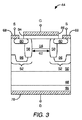
ここで図3を参照すると、本開示の一実施形態によるパワーMOSFETデバイス44が示されている。パワーMOSFETデバイス44は、基板46と、基板46の上方に形成されたドリフト層48と、ドリフト層48の上方に形成された拡散層50と、ドリフト層48とは反対側の拡散層50の表面にある1つ又は複数の接合インプラント52と、各接合インプラント52の間の接合ゲート電界効果トランジスタ(JFET)領域54とを備える。各接合インプラント52は、イオン注入プロセスによって形成することができ、深ウェル領域56、ベース領域58、及びソース領域60を含むことができる。各深ウェル領域56は、ドリフト層48とは反対側の拡散層50の角から、ドリフト層48に向かって下方に、かつ、拡散層50の中央に向かって内方に延在する。深ウェル領域56は、均一に形成されてもよく、あるいは1つ又は複数の突出領域を含んでいてもよい。各ベース領域58は、ドリフト層48とは反対側の拡散層50の表面から垂直に、それぞれの深ウェル領域56の内縁の一部分に沿ってドリフト層48に向かって下方に形成される。各ソース領域60は、ドリフト層48とは反対側の拡散層50の表面上の浅い部分に形成され、かつ、横方向に延在して、深ウェル領域56及びベース領域58の全体にわたって延在しない状態で、深ウェル領域56及びベース領域58の一部分と重なり合う。JFET領域54は、各接合インプラント52の間にチャネル幅62を画定する。
Referring now to FIG. 3, a
ゲート酸化物層64は、ドリフト層48とは反対側の拡散層50の表面上に位置し、各ソース領域60の表面の一部分の間で横方向に延在しており、ゲート酸化物層64は、接合インプラント52の各ソース領域60の表面と部分的に重なり合い、該表面の間を延びる。ゲートコンタクト66は、ゲート酸化物層64の上面に配置される。2つのソースコンタクト68はそれぞれ、ドリフト層48とは反対側の拡散層50の表面上に配置され、それにより、各ソースコンタクト68は、接合インプラント52のソース領域60及び深ウェル領域56の両方とそれぞれ部分的に重なり合い、ゲート酸化物層64又はゲートコンタクト66に接触しない。ドレインコンタクト70は、ドリフト層48とは反対側の基板46の表面上に配置される。
The
動作時、バイアス電圧がゲートコンタクト66に印加されず、ドレインコンタクト70が正にバイアスされるときに、各深ウェル領域56と拡散層50との間の接合部が逆バイアスされ、それにより、パワーMOSFET44をOFF状態にする。パワーMOSFET44のOFF状態において、ソースコンタクトとドレインコンタクトとの間の電圧はドリフト層48及び拡散層50によって支持される。パワーMOSFET44の縦型構造に起因して、デバイスに損傷を与えることなく、ソースコンタクト68とドレインコンタクト70との間に大きな電圧をかけることができる。
In operation, when no bias voltage is applied to the
図4は、デバイスがON状態にあるときのパワーMOSFET44の動作を示す。パワーMOSFET44のゲートコンタクト66に正バイアスが印加されると、反転層チャネル72がゲートコンタクト66の真下の拡散層50の表面に形成され、それにより、パワーMOSFET44をON状態にする。パワーMOSFET44のON状態において、電流(図4において影付き領域で示す)は、各ソースコンタクト68から反転層チャネル72を通ってJFET領域54内に流れることを許容される。JFET領域54内に入ると、電流は、拡散層50を通って下方に、ドレインコンタクト70に向かって流れる。深ウェル領域56と、ベース領域58と、拡散層50との間に形成される接合部によって生じる電界は、JFET領域54内の電流を、JFETチャネル幅76を有するJFETチャネル74に入るよう制限する。
FIG. 4 shows the operation of the
反転層チャネル72からのある拡散距離78において、接合インプラント52によって生じる電界が減少すると、電流は、図4に示すように、拡散層50内で横方向に分布するか又は拡散する。拡散層50は、拡散層50内の抵抗を減少させるようにドープされ、それにより、JFETチャネル幅76を増加させ、拡散距離78を減少させることによって、電界の作用を軽減する。JFETチャネル幅76を増加させ、拡散距離78を減少させることによって、拡散層50は、パワーMOSFET44のON抵抗を著しく減少させる。例えば、パワーMOSFET44のON抵抗は、デバイスが1200Vを扱うように定格付けされるときに約2.2mΩ/cm2、デバイスが600Vを扱うように定格付けされるときに約1.8mΩ/cm2とすることができる。
When at some
パワーMOSFET44のON抵抗を減少させることによって、拡散層50は、各接合インプラント52の間のチャネル幅62の減少を可能にする。パワーMOSFET44のチャネル幅62を減少させることは、デバイスの設置面積だけでなく寿命も改善する。各接合インプラント52が互いに近づくにつれて、深ウェル領域56と、ベース領域58と、拡散層50との間の接合部によって生成される電界の大部分は、反対側の接合インプラント52によって打切られる。したがって、ゲート酸化物層64が出会う電界が著しく減少し、それにより、パワーMOSFET44の寿命が改善されることになる。一実施形態によれば、パワーMOSFET44のチャネル幅62は3ミクロン未満である。
By reducing the ON resistance of the
パワーMOSFET44は、例えば、炭化ケイ素(SiC)デバイス、ヒ化ガリウム(GaAs)デバイス、又は窒化ガリウム(GAN)デバイスとすることができる。当業者であれば、本開示の概念が任意の材料系に適用可能であることを理解するであろう。パワーMOSFET44の基板46は約180〜350ミクロン厚とすることができる。ドリフト層48は、パワーMOSFET44の電圧定格に応じて、約3.5〜12ミクロン厚とすることができる。拡散層50は約1.0〜2.5ミクロン厚とすることができる。各接合インプラント52は約1.0〜2.0ミクロン厚とすることができる。JFET領域54は約0.75〜1.5ミクロン厚とすることができる。
The
一実施形態によれば、拡散層50は、約2×1017cm−3〜5×1016cm−3のドーピング濃度を有するNドープ層である。拡散層50は、ドリフト層48に最も近い拡散層50の部分が、約5×1016cm−3のドーピング濃度を有し、拡散層50が上方に延在するにつれてその濃度が約2×1017cm−3のドーピング濃度まで徐々に変化するように、漸変する。更なる実施形態によれば、拡散層50は複数の層を備えることができる。ドリフト層48に最も近い拡散層50の層は約5×1016cm−3のドーピング濃度を有することができる。拡散層の各付加的な層のドーピング濃度は、JFET領域54からのその層の距離に比例して減少してもよい。ドリフト層48に最も近い拡散層50の層は2×1017cm−3のドーピング濃度を有することができる。
According to one embodiment, the
JFET領域54は、約1×1016cm−3〜2×1017cm−3のドーピング濃度を有するNドープ層とすることができる。ドリフト層48は、約6×1015cm−3〜1.5×1016cm−3のドーピング濃度を有するNドープ層とすることができる。深ウェル領域56は、約5×1017cm−3〜1×1020cm−3のドーピング濃度を有する高濃度Pドープ領域とすることができる。ベース領域58は、約5×1016cm−3〜1×1019cm−3のドーピング濃度を有するPドープ領域とすることができる。ソース領域60は、約1×1019cm−3〜1×1021cm−3のドーピング濃度を有するNドープ領域とすることができる。Nドーピング物質は、当業者によって認識されるように、窒素、亜リン酸、又は任意の他の適した元素とすることができる。Pドーピング物質は、当業者によって認識されるように、アルミニウム、ホウ素、又は任意の他の適した元素とすることができる。
ゲートコンタクト66、ソースコンタクト68、及びドレインコンタクト70は複数の層を備えることができる。例えば、それぞれのコンタクトは、ニッケル又はニッケル−アルミニウムの第1の層と、第1の層上方のチタンの第2の層と、第2の層上方のチタン−ニッケルの第3の層と、第3の層上方のアルミニウムの第4の層とを含むことができる。当業者であれば、ゲートコンタクト66、ソースコンタクト68、及びドレインコンタクト70が任意の適した材料で形成することができることを理解するであろう。
The
図5は、本開示の更なる実施形態によるパワーMOSFET44を示す。図5に示すパワーMOSFET44は、図3のパワーMOSFET44と実質的に同様であるが、ゲート酸化物層64と拡散層50との間にチャネル再成長層80を更に含む。チャネル再成長層80は、パワーMOSFET44の閾値電圧を下げるために設けられる。特に、深ウェル領域56は、高レベルのドーピングに起因して、パワーMOSFET44の閾値電圧を、最適性能を抑制するレベルまで上げる可能性がある。したがって、チャネル再成長層80は、パワーMOSFET44の閾値電圧を下げるために、深ウェル領域56の作用を相殺してもよい。チャネル再成長層80は、約1×1015cm−3〜1×1017cm−3のドーピング濃度を有するNドープ領域とすることができる。
FIG. 5 illustrates a
図6〜15は、図3に示すパワーMOSFET44を製造するためのプロセスを示す。最初に、図6に示すように、ドリフト層48が基板46の上面で成長させられる。当業者であれば、本開示の原理から逸脱することなく、任意の適した成長プロセスを使用してドリフト層48を生成することができることを認識するであろう。例えば、化学気相堆積法を使用してドリフト層48を生成することができる。
6 to 15 show a process for manufacturing the
次に、図7で示すように、拡散層50がドリフト層48の上面で成長させられる。先に論じたように、本開示の原理から逸脱することなく、任意の適した成長プロセスを使用して拡散層50を作成することができる。一実施形態によれば、拡散層50は、漸変ドーピングプロファイルを有するように成長させられる。
Next, as shown in FIG. 7, a
次に、図8に示すように、各接合インプラント52の深ウェル領域56が、拡散層50に注入される。当業者によって理解されるように、深ウェル領域56は、任意の適した注入プロセスによって注入することができる。例えば、深ウェル領域56を形成するために、イオン注入法を使用することができる。その後、ベース領域58が図9に示すように注入され、それに続いて、ソース領域60が図10に示すように注入される。
Next, as shown in FIG. 8, the
次に、図11に示すように、JFET領域54が注入される。先に論じたように、本開示の原理から逸脱することなく、JFET領域54を作成するために、任意の適した注入プロセスを使用することができる。更に、図示しないが、JFET領域54は、代替的に、成長プロセスによって作成してもよい。
Next, as shown in FIG. 11, a
次に、図12で示すように、ゲート酸化物層64が拡散層50の上面に形成され、それにより、ゲート酸化物層64は、接合インプラント52のそれぞれのソース領域60の表面と部分的に重なり合い、該表面の間を延びる。図13において、ゲートコンタクト66がゲート酸化物層64の上面に形成される。その後、ソースコンタクト68が拡散層50の表面上に形成され、それにより、図14に示すように、各ソースコンタクト68は、接合インプラント52のソース領域60及び深ウェル領域56の両方にそれぞれ部分的に重なり合うが、ゲート酸化物層64又はゲートコンタクト66には接触しない。最後に、図15において、ドレインコンタクト70が、ドリフト層48とは反対側の基板46の表面上に設けられる。
Next, as shown in FIG. 12, a
図16は、パワーMOSFET44のON抵抗に対する拡散層の50の作用を示すグラフである。図示するように、拡散層は、デバイスのON抵抗において約20%の減少を提供する。
FIG. 16 is a graph showing the action of the
図17は、ゲート酸化物層64が出会う電界に対する拡散層50の作用を示すグラフである。拡散層50が、パワーMOSFET44の性能を妨げることなくチャネル幅62の減少を可能にするため、ゲート酸化物層64が出会う電界の最大26%が、対向する接合インプラント52によって打切られ、それにより、デバイスの寿命を著しく増加させる。
FIG. 17 is a graph showing the effect of the
当業者は、本開示の好ましい実施形態に対する改善及び改変を認識するであろう。全てのこうした改善及び改変は、本明細書に開示される概念及び添付の特許請求の範囲の範囲内にあると考えられる。 Those skilled in the art will recognize improvements and modifications to the preferred embodiments of the present disclosure. All such improvements and modifications are considered within the scope of the concepts disclosed herein and the appended claims.
Claims (13)
基板と、
前記基板上のドリフト層と、
前記ドリフト層上のN型にドープされた拡散層であって、前記ドリフト層に隣接する第1の表面と該第1の表面とは反対側の第2の表面との間に複数の層を備え、該複数の層の各層のドーピング濃度が、前記第2の表面からの距離に比例して減少する、拡散層と、
2つの接合インプラントの間の接合ゲート電界効果トランジスタ(JFET)領域であって、前記第2の表面に隣接するJFET領域と、
前記接合インプラントが、P型にドープされた深ウェル領域とP型にドープされたベース領域とを含むことと、
ゲート、ドレイン、及びソースと、
を備え、前記トランジスタデバイスのチャネル幅が3ミクロン未満であり、前記トランジスタデバイスのON抵抗が、少なくとも定格電圧600Vにおいて1.8mΩ/cm2以下である、トランジスタデバイス。 A transistor device,
A substrate,
A drift layer on the substrate;
An N-type doped diffusion layer on the drift layer, wherein a plurality of layers are provided between a first surface adjacent to the drift layer and a second surface opposite to the first surface. A diffusion layer, wherein the doping concentration of each of the plurality of layers decreases in proportion to the distance from the second surface;
A junction gate field effect transistor (JFET) region between two junction implants, adjacent to the second surface;
The junction implant includes a P-type doped deep well region and a P-type doped base region;
A gate, a drain, and a source;
The transistor device has a channel width of less than 3 microns, and the transistor device has an ON resistance of 1.8 mΩ / cm 2 or less at least at a rated voltage of 600 V.
基板と、
前記基板上のドリフト層と、
前記ドリフト層上のN型にドープされた拡散層であって、前記ドリフト層に隣接する第1の表面と該第1の表面とは反対側の第2の表面との間に複数の層を備え、該複数の層の各層のドーピング濃度が、前記第2の表面からの距離に比例して減少する、拡散層と、
2つの接合インプラントの間の接合ゲート電界効果トランジスタ(JFET)領域であって、前記第2の表面に隣接するJFET領域と、
前記接合インプラントが、P型にドープされた深ウェル領域とP型にドープされたベース領域とを含むことと、
ゲート、ドレイン、及びソースと、
を備えるトランジスタデバイス。 A transistor device,
A substrate,
A drift layer on the substrate;
An N-type doped diffusion layer on the drift layer, wherein a plurality of layers are provided between a first surface adjacent to the drift layer and a second surface opposite to the first surface. A diffusion layer, wherein the doping concentration of each of the plurality of layers decreases in proportion to the distance from the second surface;
A junction gate field effect transistor (JFET) region between two junction implants, adjacent to the second surface;
The junction implant includes a P-type doped deep well region and a P-type doped base region;
A gate, a drain, and a source;
A transistor device comprising:
Applications Claiming Priority (3)
| Application Number | Priority Date | Filing Date | Title |
|---|---|---|---|
| US13/962,295 | 2013-08-08 | ||
| US13/962,295 US9331197B2 (en) | 2013-08-08 | 2013-08-08 | Vertical power transistor device |
| PCT/US2014/049941 WO2015021154A1 (en) | 2013-08-08 | 2014-08-06 | Vertical power transistor device |
Related Child Applications (1)
| Application Number | Title | Priority Date | Filing Date |
|---|---|---|---|
| JP2018041765A Division JP6644823B2 (en) | 2013-08-08 | 2018-03-08 | Vertical power transistor device |
Publications (3)
| Publication Number | Publication Date |
|---|---|
| JP2016529720A JP2016529720A (en) | 2016-09-23 |
| JP2016529720A5 JP2016529720A5 (en) | 2017-05-25 |
| JP6306704B2 true JP6306704B2 (en) | 2018-04-04 |
Family
ID=51358122
Family Applications (2)
| Application Number | Title | Priority Date | Filing Date |
|---|---|---|---|
| JP2016533399A Active JP6306704B2 (en) | 2013-08-08 | 2014-08-06 | Vertical power transistor device |
| JP2018041765A Active JP6644823B2 (en) | 2013-08-08 | 2018-03-08 | Vertical power transistor device |
Family Applications After (1)
| Application Number | Title | Priority Date | Filing Date |
|---|---|---|---|
| JP2018041765A Active JP6644823B2 (en) | 2013-08-08 | 2018-03-08 | Vertical power transistor device |
Country Status (6)
| Country | Link |
|---|---|
| US (4) | US9331197B2 (en) |
| EP (1) | EP3031083B1 (en) |
| JP (2) | JP6306704B2 (en) |
| CN (1) | CN105431948A (en) |
| TW (1) | TWI536575B (en) |
| WO (1) | WO2015021154A1 (en) |
Cited By (1)
| Publication number | Priority date | Publication date | Assignee | Title |
|---|---|---|---|---|
| US11862687B2 (en) | 2019-10-03 | 2024-01-02 | Fuji Electric Co., Ltd. | Nitride semiconductor device and method for fabricating nitride semiconductor device |
Families Citing this family (14)
| Publication number | Priority date | Publication date | Assignee | Title |
|---|---|---|---|---|
| US9331197B2 (en) | 2013-08-08 | 2016-05-03 | Cree, Inc. | Vertical power transistor device |
| US10600903B2 (en) | 2013-09-20 | 2020-03-24 | Cree, Inc. | Semiconductor device including a power transistor device and bypass diode |
| US10868169B2 (en) | 2013-09-20 | 2020-12-15 | Cree, Inc. | Monolithically integrated vertical power transistor and bypass diode |
| CN106898652B (en) * | 2017-03-09 | 2019-06-04 | 电子科技大学 | A kind of silicon carbide VDMOS device |
| US10608102B2 (en) | 2017-09-29 | 2020-03-31 | Electronics And Telecommunications Research Institute | Semiconductor device having a drain electrode contacting an epi material inside a through-hole and method of manufacturing the same |
| US10685886B2 (en) | 2017-12-15 | 2020-06-16 | International Business Machines Corporation | Fabrication of logic devices and power devices on the same substrate |
| JP7106881B2 (en) * | 2018-02-09 | 2022-07-27 | 株式会社デンソー | Silicon carbide substrate and silicon carbide semiconductor device |
| CN110718452A (en) | 2018-07-12 | 2020-01-21 | 创能动力科技有限公司 | Silicon carbide device and method for manufacturing same |
| US11075295B2 (en) * | 2018-07-13 | 2021-07-27 | Cree, Inc. | Wide bandgap semiconductor device |
| US11069804B2 (en) | 2018-08-31 | 2021-07-20 | Alpha And Omega Semiconductor (Cayman) Ltd. | Integration of HVLDMOS with shared isolation region |
| CN112670344B (en) * | 2020-12-10 | 2022-07-22 | 复旦大学 | SiC MOSFET with gradually-changed channel and self-alignment process thereof |
| CN116137283A (en) | 2021-11-17 | 2023-05-19 | 苏州东微半导体股份有限公司 | Semiconductor super junction power device |
| TWI818652B (en) * | 2022-07-29 | 2023-10-11 | 鴻海精密工業股份有限公司 | Manufacturing method of semiconductor device |
| TWI808044B (en) * | 2022-10-27 | 2023-07-01 | 強茂股份有限公司 | Manufacturing method of forming current aperture vertical electron transistor and current aperture vertical electron transistor |
Family Cites Families (134)
| Publication number | Priority date | Publication date | Assignee | Title |
|---|---|---|---|---|
| NL7700879A (en) * | 1977-01-28 | 1978-08-01 | Philips Nv | SEMI-GUIDE DEVICE. |
| JPS5742164A (en) * | 1980-08-27 | 1982-03-09 | Hitachi Ltd | Semiconductor device |
| JPS6149474A (en) | 1984-08-17 | 1986-03-11 | Matsushita Electronics Corp | Field-effect transistor and manufacture thereof |
| US4803533A (en) | 1986-09-30 | 1989-02-07 | General Electric Company | IGT and MOSFET devices having reduced channel width |
| US4967243A (en) | 1988-07-19 | 1990-10-30 | General Electric Company | Power transistor structure with high speed integral antiparallel Schottky diode |
| US5111253A (en) | 1989-05-09 | 1992-05-05 | General Electric Company | Multicellular FET having a Schottky diode merged therewith |
| IT1247293B (en) | 1990-05-09 | 1994-12-12 | Int Rectifier Corp | POWER TRANSISTOR DEVICE PRESENTING AN ULTRA-DEEP REGION, AT A GREATER CONCENTRATION |
| JP3259330B2 (en) * | 1992-06-19 | 2002-02-25 | 株式会社日立製作所 | Method for manufacturing semiconductor device |
| US5241195A (en) | 1992-08-13 | 1993-08-31 | North Carolina State University At Raleigh | Merged P-I-N/Schottky power rectifier having extended P-I-N junction |
| JP2561413B2 (en) | 1993-02-23 | 1996-12-11 | 日産自動車株式会社 | Semiconductor device |
| US5365102A (en) | 1993-07-06 | 1994-11-15 | North Carolina State University | Schottky barrier rectifier with MOS trench |
| US5536977A (en) | 1993-11-30 | 1996-07-16 | Siliconix Incorporated | Bidirectional current blocking MOSFET for battery disconnect switching |
| JP3022598B2 (en) | 1994-03-04 | 2000-03-21 | シーメンス アクチエンゲゼルシヤフト | Silicon carbide based MIS structure with high latch-up resistance |
| US5674766A (en) | 1994-12-30 | 1997-10-07 | Siliconix Incorporated | Method of making a trench MOSFET with multi-resistivity drain to provide low on-resistance by varying dopant concentration in epitaxial layer |
| US5973367A (en) | 1995-10-13 | 1999-10-26 | Siliconix Incorporated | Multiple gated MOSFET for use in DC-DC converter |
| JPH09146329A (en) | 1995-11-20 | 1997-06-06 | Fuji Xerox Co Ltd | Image forming device |
| US5689144A (en) | 1996-05-15 | 1997-11-18 | Siliconix Incorporated | Four-terminal power MOSFET switch having reduced threshold voltage and on-resistance |
| US5886383A (en) | 1997-01-10 | 1999-03-23 | International Rectifier Corporation | Integrated schottky diode and mosgated device |
| US6057558A (en) | 1997-03-05 | 2000-05-02 | Denson Corporation | Silicon carbide semiconductor device and manufacturing method thereof |
| US5925910A (en) | 1997-03-28 | 1999-07-20 | Stmicroelectronics, Inc. | DMOS transistors with schottky diode body structure |
| US6239463B1 (en) | 1997-08-28 | 2001-05-29 | Siliconix Incorporated | Low resistance power MOSFET or other device containing silicon-germanium layer |
| US7084456B2 (en) | 1999-05-25 | 2006-08-01 | Advanced Analogic Technologies, Inc. | Trench MOSFET with recessed clamping diode using graded doping |
| JP2006210368A (en) | 1999-07-02 | 2006-08-10 | Toyota Central Res & Dev Lab Inc | Vertical semiconductor device and its fabrication process |
| US7186609B2 (en) | 1999-12-30 | 2007-03-06 | Siliconix Incorporated | Method of fabricating trench junction barrier rectifier |
| FR2814855B1 (en) | 2000-10-03 | 2003-10-31 | St Microelectronics Sa | SCHOTTKY JUNCTION WITH STABLE BARRIER ON SILICON CARBIDE |
| US6956238B2 (en) | 2000-10-03 | 2005-10-18 | Cree, Inc. | Silicon carbide power metal-oxide semiconductor field effect transistors having a shorting channel and methods of fabricating silicon carbide metal-oxide semiconductor field effect transistors having a shorting channel |
| EP1204145B1 (en) | 2000-10-23 | 2011-12-28 | Panasonic Corporation | Semiconductor element |
| EP1396030B1 (en) * | 2001-04-11 | 2011-06-29 | Silicon Semiconductor Corporation | Vertical power semiconductor device and method of making the same |
| US6683363B2 (en) | 2001-07-03 | 2004-01-27 | Fairchild Semiconductor Corporation | Trench structure for semiconductor devices |
| US6621107B2 (en) | 2001-08-23 | 2003-09-16 | General Semiconductor, Inc. | Trench DMOS transistor with embedded trench schottky rectifier |
| JP4097417B2 (en) | 2001-10-26 | 2008-06-11 | 株式会社ルネサステクノロジ | Semiconductor device |
| GB0202437D0 (en) | 2002-02-02 | 2002-03-20 | Koninkl Philips Electronics Nv | Cellular mosfet devices and their manufacture |
| US6855970B2 (en) | 2002-03-25 | 2005-02-15 | Kabushiki Kaisha Toshiba | High-breakdown-voltage semiconductor device |
| US7701001B2 (en) | 2002-05-03 | 2010-04-20 | International Rectifier Corporation | Short channel trench power MOSFET with low threshold voltage |
| US7221010B2 (en) * | 2002-12-20 | 2007-05-22 | Cree, Inc. | Vertical JFET limited silicon carbide power metal-oxide semiconductor field effect transistors |
| CN100544026C (en) | 2002-12-20 | 2009-09-23 | 克里公司 | Silicon carbide power metal-oxide semiconductor field effect transistors and manufacture method |
| US7169634B2 (en) | 2003-01-15 | 2007-01-30 | Advanced Power Technology, Inc. | Design and fabrication of rugged FRED |
| JP3964819B2 (en) | 2003-04-07 | 2007-08-22 | 株式会社東芝 | Insulated gate semiconductor device |
| US6979863B2 (en) | 2003-04-24 | 2005-12-27 | Cree, Inc. | Silicon carbide MOSFETs with integrated antiparallel junction barrier Schottky free wheeling diodes and methods of fabricating the same |
| US7638841B2 (en) | 2003-05-20 | 2009-12-29 | Fairchild Semiconductor Corporation | Power semiconductor devices and methods of manufacture |
| JP2005011846A (en) | 2003-06-16 | 2005-01-13 | Nissan Motor Co Ltd | Semiconductor device |
| JP4799829B2 (en) | 2003-08-27 | 2011-10-26 | 三菱電機株式会社 | Insulated gate transistor and inverter circuit |
| JP2005302925A (en) * | 2004-04-09 | 2005-10-27 | Toshiba Corp | Semiconductor device |
| JP4899405B2 (en) | 2004-11-08 | 2012-03-21 | 株式会社デンソー | Silicon carbide semiconductor device and manufacturing method thereof |
| DE102004053761A1 (en) | 2004-11-08 | 2006-05-18 | Robert Bosch Gmbh | Semiconductor device and method for its production |
| DE102004053760A1 (en) | 2004-11-08 | 2006-05-11 | Robert Bosch Gmbh | Semiconductor device and method for its production |
| US7498633B2 (en) | 2005-01-21 | 2009-03-03 | Purdue Research Foundation | High-voltage power semiconductor device |
| US8836015B2 (en) | 2005-02-11 | 2014-09-16 | Alpha And Omega Semiconductor Incorporated | Planar SRFET using no additional masks and layout method |
| US8110869B2 (en) | 2005-02-11 | 2012-02-07 | Alpha & Omega Semiconductor, Ltd | Planar SRFET using no additional masks and layout method |
| US8362547B2 (en) | 2005-02-11 | 2013-01-29 | Alpha & Omega Semiconductor Limited | MOS device with Schottky barrier controlling layer |
| US7436022B2 (en) | 2005-02-11 | 2008-10-14 | Alpha & Omega Semiconductors, Ltd. | Enhancing Schottky breakdown voltage (BV) without affecting an integrated MOSFET-Schottky device layout |
| US7737522B2 (en) | 2005-02-11 | 2010-06-15 | Alpha & Omega Semiconductor, Ltd. | Trench junction barrier controlled Schottky device with top and bottom doped regions for enhancing forward current in a vertical direction |
| JP4916671B2 (en) | 2005-03-31 | 2012-04-18 | 住友電工デバイス・イノベーション株式会社 | Semiconductor device |
| JP2006344759A (en) * | 2005-06-08 | 2006-12-21 | Sharp Corp | Trench type mosfet and its fabrication process |
| US20070012983A1 (en) | 2005-07-15 | 2007-01-18 | Yang Robert K | Terminations for semiconductor devices with floating vertical series capacitive structures |
| US8461648B2 (en) | 2005-07-27 | 2013-06-11 | Infineon Technologies Austria Ag | Semiconductor component with a drift region and a drift control region |
| KR100674862B1 (en) * | 2005-08-25 | 2007-01-29 | 삼성전기주식회사 | Nitride semiconductor light emitting device |
| US7928470B2 (en) | 2005-11-25 | 2011-04-19 | Denso Corporation | Semiconductor device having super junction MOS transistor and method for manufacturing the same |
| US7696598B2 (en) | 2005-12-27 | 2010-04-13 | Qspeed Semiconductor Inc. | Ultrafast recovery diode |
| JP4727426B2 (en) | 2006-01-10 | 2011-07-20 | 三菱電機株式会社 | Semiconductor device and manufacturing method of semiconductor device |
| JP5017865B2 (en) * | 2006-01-17 | 2012-09-05 | 富士電機株式会社 | Semiconductor device |
| DE112006003742B4 (en) | 2006-02-07 | 2015-06-03 | Mitsubishi Electric Corp. | Semiconductor device and method of making the same |
| JP4900662B2 (en) | 2006-03-02 | 2012-03-21 | 独立行政法人産業技術総合研究所 | Silicon carbide MOS field effect transistor with built-in Schottky diode and manufacturing method thereof |
| JP5560519B2 (en) | 2006-04-11 | 2014-07-30 | 日産自動車株式会社 | Semiconductor device and manufacturing method thereof |
| JP2008016747A (en) | 2006-07-10 | 2008-01-24 | Fuji Electric Holdings Co Ltd | Trench-mos silicon carbide semiconductor device and method for manufacturing the same |
| WO2008020911A2 (en) | 2006-08-17 | 2008-02-21 | Cree, Inc. | High power insulated gate bipolar transistors |
| US7595241B2 (en) | 2006-08-23 | 2009-09-29 | General Electric Company | Method for fabricating silicon carbide vertical MOSFET devices |
| JP2008053448A (en) | 2006-08-24 | 2008-03-06 | Rohm Co Ltd | Mis-type field effect transistor and manufacturing method thereof |
| JP4863468B2 (en) * | 2006-09-15 | 2012-01-25 | 三菱レイヨン株式会社 | Manufacturing method of optical disk |
| WO2008069309A1 (en) | 2006-12-07 | 2008-06-12 | Shindengen Electric Manufacturing Co., Ltd. | Semiconductor device and method for manufacturing the same |
| US20080142811A1 (en) * | 2006-12-13 | 2008-06-19 | General Electric Company | MOSFET devices and methods of fabrication |
| JP4412335B2 (en) | 2007-02-23 | 2010-02-10 | 株式会社デンソー | Method for manufacturing silicon carbide semiconductor device |
| JP4450241B2 (en) | 2007-03-20 | 2010-04-14 | 株式会社デンソー | Method for manufacturing silicon carbide semiconductor device |
| US7982239B2 (en) | 2007-06-13 | 2011-07-19 | Northrop Grumman Corporation | Power switching transistors |
| WO2008153142A1 (en) | 2007-06-15 | 2008-12-18 | Rohm Co., Ltd. | Semiconductor device |
| JP4492735B2 (en) | 2007-06-20 | 2010-06-30 | 株式会社デンソー | Semiconductor device and manufacturing method of semiconductor device |
| JP4599379B2 (en) | 2007-08-31 | 2010-12-15 | 株式会社東芝 | Trench gate type semiconductor device |
| US7687825B2 (en) | 2007-09-18 | 2010-03-30 | Cree, Inc. | Insulated gate bipolar conduction transistors (IBCTS) and related methods of fabrication |
| US7772621B2 (en) | 2007-09-20 | 2010-08-10 | Infineon Technologies Austria Ag | Semiconductor device with structured current spread region and method |
| US7579632B2 (en) | 2007-09-21 | 2009-08-25 | Semiconductor Components Industries, L.L.C. | Multi-channel ESD device and method therefor |
| JP2009094203A (en) | 2007-10-05 | 2009-04-30 | Denso Corp | Silicon carbide semiconductor device |
| US7943987B2 (en) | 2007-10-18 | 2011-05-17 | Infineon Technologies Austria Ag | Semiconductor component with a drift zone and a drift control zone |
| DE102007057674A1 (en) * | 2007-11-30 | 2009-06-04 | Osram Opto Semiconductors Gmbh | LED with current spreading layer |
| US7989882B2 (en) | 2007-12-07 | 2011-08-02 | Cree, Inc. | Transistor with A-face conductive channel and trench protecting well region |
| US20090179297A1 (en) | 2008-01-16 | 2009-07-16 | Northrop Grumman Systems Corporation | Junction barrier schottky diode with highly-doped channel region and methods |
| US7795691B2 (en) | 2008-01-25 | 2010-09-14 | Cree, Inc. | Semiconductor transistor with P type re-grown channel layer |
| JP5369464B2 (en) | 2008-03-24 | 2013-12-18 | 富士電機株式会社 | Silicon carbide MOS type semiconductor device |
| JP5617175B2 (en) | 2008-04-17 | 2014-11-05 | 富士電機株式会社 | Wide band gap semiconductor device and manufacturing method thereof |
| JP5326405B2 (en) | 2008-07-30 | 2013-10-30 | 株式会社デンソー | Wide band gap semiconductor device |
| JP2010081043A (en) | 2008-09-24 | 2010-04-08 | Oki Semiconductor Co Ltd | H-bridge circuit |
| US7906427B2 (en) | 2008-10-14 | 2011-03-15 | General Electric Company | Dimension profiling of SiC devices |
| JP2012114104A (en) * | 2009-02-24 | 2012-06-14 | Hitachi Ltd | Storage insulation gate type field effect transistor |
| JP5453903B2 (en) | 2009-04-28 | 2014-03-26 | 富士電機株式会社 | Wide band gap semiconductor device |
| DE102009033302B4 (en) | 2009-07-15 | 2012-01-26 | Infineon Technologies Ag | Manufacturing Method for a Unipolar Semiconductor Device and Semiconductor Device |
| US8283973B2 (en) | 2009-08-19 | 2012-10-09 | Panasonic Corporation | Semiconductor element, semiconductor device, and electric power converter |
| US8829614B2 (en) | 2009-08-31 | 2014-09-09 | Alpha And Omega Semiconductor Incorporated | Integrated Schottky diode in high voltage semiconductor device |
| US20110156810A1 (en) | 2009-12-30 | 2011-06-30 | Intersil Americas Inc. | Integrated dmos and schottky |
| WO2011105434A1 (en) | 2010-02-23 | 2011-09-01 | 富士電機ホールディングス株式会社 | Semiconductor device |
| JP2011228643A (en) * | 2010-03-30 | 2011-11-10 | Shindengen Electric Mfg Co Ltd | Semiconductor device and manufacturing method thereof |
| US8415671B2 (en) * | 2010-04-16 | 2013-04-09 | Cree, Inc. | Wide band-gap MOSFETs having a heterojunction under gate trenches thereof and related methods of forming such devices |
| US8581341B2 (en) | 2010-04-20 | 2013-11-12 | Maxpower Semiconductor, Inc. | Power MOSFET with embedded recessed field plate and methods of fabrication |
| DE102011079747A1 (en) | 2010-07-27 | 2012-02-02 | Denso Corporation | Semiconductor device with switching element and freewheeling diode, and control method therefor |
| DE102010039258B4 (en) | 2010-08-12 | 2018-03-15 | Infineon Technologies Austria Ag | Transistor device with reduced short-circuit current |
| EP2628186A4 (en) * | 2010-10-12 | 2015-11-25 | Silanna Semiconductor Usa Inc | Vertical semiconductor device with thinned substrate |
| WO2012056719A1 (en) | 2010-10-29 | 2012-05-03 | パナソニック株式会社 | Converter |
| CN102097560B (en) * | 2010-12-31 | 2012-11-14 | 厦门市三安光电科技有限公司 | Nitride light emitting diode having composite double current spreading layer |
| WO2012105609A1 (en) | 2011-02-02 | 2012-08-09 | ローム株式会社 | Semiconductor device |
| JP5498431B2 (en) | 2011-02-02 | 2014-05-21 | ローム株式会社 | Semiconductor device and manufacturing method thereof |
| US8575692B2 (en) * | 2011-02-11 | 2013-11-05 | Freescale Semiconductor, Inc. | Near zero channel length field drift LDMOS |
| JP5881322B2 (en) | 2011-04-06 | 2016-03-09 | ローム株式会社 | Semiconductor device |
| CN103460390B (en) | 2011-04-08 | 2017-03-08 | 富士电机株式会社 | Silicon carbide vertical field-effect transistor |
| US9349797B2 (en) * | 2011-05-16 | 2016-05-24 | Cree, Inc. | SiC devices with high blocking voltage terminated by a negative bevel |
| JP5874723B2 (en) * | 2011-05-18 | 2016-03-02 | 富士電機株式会社 | Semiconductor device and manufacturing method of semiconductor device |
| JP2012243966A (en) | 2011-05-20 | 2012-12-10 | Sumitomo Electric Ind Ltd | Semiconductor device |
| US20120306009A1 (en) | 2011-06-03 | 2012-12-06 | Suku Kim | Integration of superjunction mosfet and diode |
| CN103069571B (en) | 2011-06-27 | 2015-11-25 | 松下电器产业株式会社 | Silicon carbide semiconductor device and manufacture method thereof |
| CN107068733B (en) | 2011-07-27 | 2020-08-11 | 丰田自动车株式会社 | Semiconductor device with a plurality of transistors |
| JP2013030618A (en) | 2011-07-28 | 2013-02-07 | Rohm Co Ltd | Semiconductor device |
| JP5745997B2 (en) | 2011-10-31 | 2015-07-08 | トヨタ自動車株式会社 | Switching element and manufacturing method thereof |
| JP2013125827A (en) | 2011-12-14 | 2013-06-24 | Toshiba Corp | Semiconductor device and method of manufacturing the same |
| JP5677330B2 (en) * | 2012-01-20 | 2015-02-25 | 三菱電機株式会社 | Silicon carbide semiconductor device and manufacturing method thereof |
| CN102738334B (en) * | 2012-06-19 | 2015-07-08 | 厦门市三安光电科技有限公司 | Light emitting diode with current spreading layers and manufacturing method for light emitting diode |
| US9214521B2 (en) | 2012-06-21 | 2015-12-15 | Infineon Technologies Ag | Reverse conducting IGBT |
| US8637922B1 (en) | 2012-07-19 | 2014-01-28 | Infineon Technologies Ag | Semiconductor device |
| US8901639B2 (en) | 2012-07-26 | 2014-12-02 | Cree, Inc. | Monolithic bidirectional silicon carbide switching devices |
| US9166048B2 (en) * | 2012-09-16 | 2015-10-20 | Sensor Electronic Technology, Inc. | Lateral/vertical semiconductor device |
| JP6082229B2 (en) | 2012-10-30 | 2017-02-15 | 住友化学株式会社 | Nitride semiconductor device and manufacturing method thereof |
| CN103151371A (en) * | 2013-03-05 | 2013-06-12 | 矽力杰半导体技术(杭州)有限公司 | Wafer structure and power device by using same |
| JP6135364B2 (en) | 2013-07-26 | 2017-05-31 | 住友電気工業株式会社 | Silicon carbide semiconductor device and manufacturing method thereof |
| US9331197B2 (en) | 2013-08-08 | 2016-05-03 | Cree, Inc. | Vertical power transistor device |
| US10600903B2 (en) | 2013-09-20 | 2020-03-24 | Cree, Inc. | Semiconductor device including a power transistor device and bypass diode |
| US20150084063A1 (en) | 2013-09-20 | 2015-03-26 | Cree, Inc. | Semiconductor device with a current spreading layer |
| US10868169B2 (en) | 2013-09-20 | 2020-12-15 | Cree, Inc. | Monolithically integrated vertical power transistor and bypass diode |
| US9318597B2 (en) | 2013-09-20 | 2016-04-19 | Cree, Inc. | Layout configurations for integrating schottky contacts into a power transistor device |
-
2013
- 2013-08-08 US US13/962,295 patent/US9331197B2/en not_active Ceased
-
2014
- 2014-08-06 EP EP14752742.8A patent/EP3031083B1/en active Active
- 2014-08-06 JP JP2016533399A patent/JP6306704B2/en active Active
- 2014-08-06 WO PCT/US2014/049941 patent/WO2015021154A1/en active Application Filing
- 2014-08-06 CN CN201480044619.0A patent/CN105431948A/en active Pending
- 2014-08-07 TW TW103127134A patent/TWI536575B/en active
-
2016
- 2016-03-31 US US15/087,406 patent/US9741842B2/en active Active
-
2018
- 2018-03-08 JP JP2018041765A patent/JP6644823B2/en active Active
- 2018-05-03 US US15/970,148 patent/USRE48380E1/en active Active
-
2020
- 2020-10-26 US US17/080,062 patent/USRE49913E1/en active Active
Cited By (1)
| Publication number | Priority date | Publication date | Assignee | Title |
|---|---|---|---|---|
| US11862687B2 (en) | 2019-10-03 | 2024-01-02 | Fuji Electric Co., Ltd. | Nitride semiconductor device and method for fabricating nitride semiconductor device |
Also Published As
| Publication number | Publication date |
|---|---|
| USRE48380E1 (en) | 2021-01-05 |
| US20160211360A1 (en) | 2016-07-21 |
| JP2018125544A (en) | 2018-08-09 |
| US9741842B2 (en) | 2017-08-22 |
| EP3031083A1 (en) | 2016-06-15 |
| EP3031083B1 (en) | 2021-04-14 |
| WO2015021154A1 (en) | 2015-02-12 |
| JP2016529720A (en) | 2016-09-23 |
| TWI536575B (en) | 2016-06-01 |
| US20150041886A1 (en) | 2015-02-12 |
| US9331197B2 (en) | 2016-05-03 |
| JP6644823B2 (en) | 2020-02-12 |
| TW201515225A (en) | 2015-04-16 |
| USRE49913E1 (en) | 2024-04-09 |
| CN105431948A (en) | 2016-03-23 |
Similar Documents
| Publication | Publication Date | Title |
|---|---|---|
| JP6644823B2 (en) | Vertical power transistor device | |
| JP6475635B2 (en) | Semiconductor device with reduced electric field in gate oxide layer | |
| US10950719B2 (en) | Seminconductor device with spreading layer | |
| US9111919B2 (en) | Field effect device with enhanced gate dielectric structure | |
| US10573712B2 (en) | Super-junction structure and method for manufacturing the same and semiconductor device thereof | |
| US9281392B2 (en) | Charge compensation structure and manufacturing therefor | |
| US20150084063A1 (en) | Semiconductor device with a current spreading layer | |
| JP6888956B2 (en) | Wide bandgap IGBT structure for semiconductor materials | |
| US10615274B2 (en) | Vertical semiconductor device with improved ruggedness | |
| WO2019186785A1 (en) | Silicon carbide semiconductor device and production method therefor | |
| JP2019531601A (en) | Trench vertical JFET with improved threshold voltage control | |
| KR101598512B1 (en) | Junction barrier schottky diode having epi Re-growth pattern and method for producing same | |
| US20230369445A1 (en) | Vertical power devices having mesas and etched trenches therebetween | |
| JP2020035868A (en) | Method of manufacturing semiconductor device | |
| KR20150093351A (en) | Silicon Carbide MOSFET | |
| KR20150093349A (en) | Silicon Carbide MOSFET |
Legal Events
| Date | Code | Title | Description |
|---|---|---|---|
| A521 | Request for written amendment filed |
Free format text: JAPANESE INTERMEDIATE CODE: A523 Effective date: 20170404 |
|
| A621 | Written request for application examination |
Free format text: JAPANESE INTERMEDIATE CODE: A621 Effective date: 20170404 |
|
| A131 | Notification of reasons for refusal |
Free format text: JAPANESE INTERMEDIATE CODE: A131 Effective date: 20170822 |
|
| A521 | Request for written amendment filed |
Free format text: JAPANESE INTERMEDIATE CODE: A523 Effective date: 20171121 |
|
| TRDD | Decision of grant or rejection written | ||
| A01 | Written decision to grant a patent or to grant a registration (utility model) |
Free format text: JAPANESE INTERMEDIATE CODE: A01 Effective date: 20180206 |
|
| A61 | First payment of annual fees (during grant procedure) |
Free format text: JAPANESE INTERMEDIATE CODE: A61 Effective date: 20180308 |
|
| R150 | Certificate of patent or registration of utility model |
Ref document number: 6306704 Country of ref document: JP Free format text: JAPANESE INTERMEDIATE CODE: R150 |
|
| R250 | Receipt of annual fees |
Free format text: JAPANESE INTERMEDIATE CODE: R250 |
|
| R250 | Receipt of annual fees |
Free format text: JAPANESE INTERMEDIATE CODE: R250 |
|
| S533 | Written request for registration of change of name |
Free format text: JAPANESE INTERMEDIATE CODE: R313533 |
|
| R350 | Written notification of registration of transfer |
Free format text: JAPANESE INTERMEDIATE CODE: R350 |
|
| R250 | Receipt of annual fees |
Free format text: JAPANESE INTERMEDIATE CODE: R250 |
|
| R250 | Receipt of annual fees |
Free format text: JAPANESE INTERMEDIATE CODE: R250 |