JP6298249B2 - NONVOLATILE MEMORY DEVICE, MEMORY SYSTEM INCLUDING THE SAME, AND MEMORY BLOCK MANAGEMENT, ERASE AND PROGRAM METHOD THEREOF - Google Patents
NONVOLATILE MEMORY DEVICE, MEMORY SYSTEM INCLUDING THE SAME, AND MEMORY BLOCK MANAGEMENT, ERASE AND PROGRAM METHOD THEREOF Download PDFInfo
- Publication number
- JP6298249B2 JP6298249B2 JP2013144492A JP2013144492A JP6298249B2 JP 6298249 B2 JP6298249 B2 JP 6298249B2 JP 2013144492 A JP2013144492 A JP 2013144492A JP 2013144492 A JP2013144492 A JP 2013144492A JP 6298249 B2 JP6298249 B2 JP 6298249B2
- Authority
- JP
- Japan
- Prior art keywords
- erase
- memory
- emergency
- state
- voltage
- Prior art date
- Legal status (The legal status is an assumption and is not a legal conclusion. Google has not performed a legal analysis and makes no representation as to the accuracy of the status listed.)
- Active
Links
- PWPJGUXAGUPAHP-UHFFFAOYSA-N lufenuron Chemical compound C1=C(Cl)C(OC(F)(F)C(C(F)(F)F)F)=CC(Cl)=C1NC(=O)NC(=O)C1=C(F)C=CC=C1F PWPJGUXAGUPAHP-UHFFFAOYSA-N 0.000 title 1
- 238000000034 method Methods 0.000 claims description 43
- 238000012795 verification Methods 0.000 claims description 31
- 230000004044 response Effects 0.000 claims description 18
- 238000011084 recovery Methods 0.000 claims description 6
- 238000007667 floating Methods 0.000 claims description 2
- 238000007599 discharging Methods 0.000 claims 1
- 238000010586 diagram Methods 0.000 description 38
- 238000007726 management method Methods 0.000 description 19
- 239000000872 buffer Substances 0.000 description 7
- 238000012937 correction Methods 0.000 description 7
- 239000004065 semiconductor Substances 0.000 description 5
- 238000003860 storage Methods 0.000 description 5
- 101100481702 Arabidopsis thaliana TMK1 gene Proteins 0.000 description 4
- 238000004891 communication Methods 0.000 description 4
- 238000009826 distribution Methods 0.000 description 4
- 239000000758 substrate Substances 0.000 description 4
- 230000008030 elimination Effects 0.000 description 2
- 238000003379 elimination reaction Methods 0.000 description 2
- 238000012545 processing Methods 0.000 description 2
- 238000012552 review Methods 0.000 description 2
- 101100028951 Homo sapiens PDIA2 gene Proteins 0.000 description 1
- 102100036351 Protein disulfide-isomerase A2 Human genes 0.000 description 1
- 238000003491 array Methods 0.000 description 1
- 230000003139 buffering effect Effects 0.000 description 1
- 239000000919 ceramic Substances 0.000 description 1
- 238000013500 data storage Methods 0.000 description 1
- 230000009977 dual effect Effects 0.000 description 1
- 238000005516 engineering process Methods 0.000 description 1
- 238000007429 general method Methods 0.000 description 1
- 230000005415 magnetization Effects 0.000 description 1
- 230000014759 maintenance of location Effects 0.000 description 1
- 238000004519 manufacturing process Methods 0.000 description 1
- 238000012986 modification Methods 0.000 description 1
- 230000004048 modification Effects 0.000 description 1
- 238000012546 transfer Methods 0.000 description 1
Images


Classifications
-
- G—PHYSICS
- G11—INFORMATION STORAGE
- G11C—STATIC STORES
- G11C16/00—Erasable programmable read-only memories
- G11C16/02—Erasable programmable read-only memories electrically programmable
- G11C16/06—Auxiliary circuits, e.g. for writing into memory
- G11C16/10—Programming or data input circuits
- G11C16/14—Circuits for erasing electrically, e.g. erase voltage switching circuits
- G11C16/16—Circuits for erasing electrically, e.g. erase voltage switching circuits for erasing blocks, e.g. arrays, words, groups
-
- G—PHYSICS
- G06—COMPUTING; CALCULATING OR COUNTING
- G06F—ELECTRIC DIGITAL DATA PROCESSING
- G06F12/00—Accessing, addressing or allocating within memory systems or architectures
- G06F12/02—Addressing or allocation; Relocation
- G06F12/0223—User address space allocation, e.g. contiguous or non contiguous base addressing
- G06F12/023—Free address space management
- G06F12/0238—Memory management in non-volatile memory, e.g. resistive RAM or ferroelectric memory
- G06F12/0246—Memory management in non-volatile memory, e.g. resistive RAM or ferroelectric memory in block erasable memory, e.g. flash memory
-
- G—PHYSICS
- G06—COMPUTING; CALCULATING OR COUNTING
- G06F—ELECTRIC DIGITAL DATA PROCESSING
- G06F12/00—Accessing, addressing or allocating within memory systems or architectures
- G06F12/02—Addressing or allocation; Relocation
- G06F12/0223—User address space allocation, e.g. contiguous or non contiguous base addressing
- G06F12/023—Free address space management
- G06F12/0253—Garbage collection, i.e. reclamation of unreferenced memory
-
- G—PHYSICS
- G11—INFORMATION STORAGE
- G11C—STATIC STORES
- G11C11/00—Digital stores characterised by the use of particular electric or magnetic storage elements; Storage elements therefor
- G11C11/56—Digital stores characterised by the use of particular electric or magnetic storage elements; Storage elements therefor using storage elements with more than two stable states represented by steps, e.g. of voltage, current, phase, frequency
- G11C11/5671—Digital stores characterised by the use of particular electric or magnetic storage elements; Storage elements therefor using storage elements with more than two stable states represented by steps, e.g. of voltage, current, phase, frequency using charge trapping in an insulator
-
- G—PHYSICS
- G11—INFORMATION STORAGE
- G11C—STATIC STORES
- G11C16/00—Erasable programmable read-only memories
- G11C16/02—Erasable programmable read-only memories electrically programmable
- G11C16/04—Erasable programmable read-only memories electrically programmable using variable threshold transistors, e.g. FAMOS
- G11C16/0408—Erasable programmable read-only memories electrically programmable using variable threshold transistors, e.g. FAMOS comprising cells containing floating gate transistors
- G11C16/0416—Erasable programmable read-only memories electrically programmable using variable threshold transistors, e.g. FAMOS comprising cells containing floating gate transistors comprising cells containing a single floating gate transistor and no select transistor, e.g. UV EPROM
-
- G—PHYSICS
- G11—INFORMATION STORAGE
- G11C—STATIC STORES
- G11C16/00—Erasable programmable read-only memories
- G11C16/02—Erasable programmable read-only memories electrically programmable
- G11C16/04—Erasable programmable read-only memories electrically programmable using variable threshold transistors, e.g. FAMOS
- G11C16/0466—Erasable programmable read-only memories electrically programmable using variable threshold transistors, e.g. FAMOS comprising cells with charge storage in an insulating layer, e.g. metal-nitride-oxide-silicon [MNOS], silicon-oxide-nitride-oxide-silicon [SONOS]
-
- G—PHYSICS
- G11—INFORMATION STORAGE
- G11C—STATIC STORES
- G11C16/00—Erasable programmable read-only memories
- G11C16/02—Erasable programmable read-only memories electrically programmable
- G11C16/06—Auxiliary circuits, e.g. for writing into memory
- G11C16/34—Determination of programming status, e.g. threshold voltage, overprogramming or underprogramming, retention
- G11C16/3436—Arrangements for verifying correct programming or erasure
- G11C16/344—Arrangements for verifying correct erasure or for detecting overerased cells
- G11C16/3445—Circuits or methods to verify correct erasure of nonvolatile memory cells
-
- G—PHYSICS
- G06—COMPUTING; CALCULATING OR COUNTING
- G06F—ELECTRIC DIGITAL DATA PROCESSING
- G06F2212/00—Indexing scheme relating to accessing, addressing or allocation within memory systems or architectures
- G06F2212/72—Details relating to flash memory management
- G06F2212/7205—Cleaning, compaction, garbage collection, erase control
Description
本発明は不揮発性メモリ装置とそれを含むメモリシステム及びそれらのメモリブロック管理、消去、プログラム方法に関する。 The present invention relates to a nonvolatile memory device, a memory system including the nonvolatile memory device, and a memory block management, erasure, and programming method thereof.
半導体メモリ装置は大きく揮発性半導体メモリ装置と不揮発性半導体メモリ装置とに分けられる。不揮発性半導体メモリ装置は電源が遮断されてもデータを保存できる。不揮発性メモリに格納されるデータはメモリ製造技術によって、永久的であるか、或いは再プログラムできる。不揮発性半導体メモリ装置はコンピュータ、航空電子工学、通信、及び消費者電子技術産業のような広い範囲の応用で使用者データの格納、プログラム及びマイクロコードの格納のために使用される。 Semiconductor memory devices are roughly classified into volatile semiconductor memory devices and non-volatile semiconductor memory devices. The nonvolatile semiconductor memory device can store data even when the power is turned off. The data stored in the non-volatile memory can be permanent or reprogrammed depending on the memory manufacturing technology. Non-volatile semiconductor memory devices are used for user data storage, program and microcode storage in a wide range of applications such as computers, avionics, communications, and consumer electronics industries.
本発明の目的は、より速い消去動作を実行する不揮発性メモリ装置及びそれを含むメモリシステムを提供することにある。
本発明の更に他の目的は、より速いプログラム動作を実行する不揮発性メモリ装置及びそれを含むメモリシステムを提供することにある。
An object of the present invention is to provide a non-volatile memory device that performs faster erase operation and a memory system including the same.
It is still another object of the present invention to provide a nonvolatile memory device that executes faster program operation and a memory system including the same.
本発明の実施形態による不揮発性メモリ装置の消去方法は、消去モードを設定する段階と、前記設定された消去モードにしたがって正常消去動作及び緊急消去動作の中でいずれか1つを実行する段階と、を含み、前記正常消去動作はメモリセルの閾値電圧を第1消去検証レベルより低い消去状態にセットし、前記緊急消去動作はメモリセルの閾値電圧を第2消去検証レベルより低い擬似消去状態にセットする。 A method for erasing a nonvolatile memory device according to an embodiment of the present invention includes: setting an erase mode; and executing one of a normal erase operation and an emergency erase operation according to the set erase mode; The normal erase operation sets the threshold voltage of the memory cell to an erase state lower than the first erase verify level, and the emergency erase operation sets the threshold voltage of the memory cell to a pseudo erase state lower than the second erase verify level. set.
本発明の実施形態による複数のメモリブロックを有する少なくとも1つの不揮発性メモリ装置及び前記少なくとも1つの不揮発性メモリ装置を制御するメモリ制御器を含むメモリシステムのブロック管理方法は、メモリブロックにM(Mは自然数)−ビットプログラム動作を実行する段階と、前記M−ビットプログラム動作以後に前記メモリブロックに消去動作が必要である時、前記メモリブロックのメモリセルの閾値電圧を擬似消去状態にセットする緊急消去動作を実行する段階と、前記メモリブロックに前記擬似消去状態を利用するN(Nは正の整数)−ビットプログラム動作を実行する段階と、前記N−ビットプログラム動作以後に前記メモリブロックに消去動作が必要である時、前記メモリブロックのメモリセルの閾値電圧を消去状態にセットする正常消去動作を実行する段階と、を含み、前記消去状態は第1消去検証レベルより低く、前記擬似消去状態は第2消去検証レベルより低く、前記第2消去検証レベルは前記第1消去検証レベルより高い。 A block management method of a memory system including at least one nonvolatile memory device having a plurality of memory blocks and a memory controller for controlling the at least one nonvolatile memory device according to an embodiment of the present invention includes: M (M Is a natural number) —a step of executing a bit program operation, and an emergency operation to set the threshold voltage of the memory cell of the memory block to a pseudo erase state when the memory block needs to be erased after the M-bit program operation. Performing an erase operation; performing an N (N is a positive integer) -bit program operation utilizing the pseudo erase state for the memory block; and erasing the memory block after the N-bit program operation. When operation is necessary, the threshold voltage of the memory cell in the memory block is erased. Performing a normal erase operation to set the erase state to be lower than a first erase verify level, the pseudo erase state is lower than a second erase verify level, and the second erase verify level is higher than the first erase verify level. Higher than erase verification level.
本発明の実施形態による不揮発性メモリ装置及び前記不揮発性メモリ装置を制御するメモリ制御器を含むメモリシステムのプログラム方法は、データ及びアドレスが入力される段階と、消去動作が必要であるか否かを判別する段階と、前記消去動作が必要である時、緊急消去動作が必要であるか否かを判別する段階と、前記緊急消去動作が必要である時擬似消去状態にセットする前記緊急消去動作を実行する段階と、前記緊急消去動作が必要でない時、消去状態にセットする正常消去動作を実行する段階と、前記消去動作の以後に前記入力されたデータに対して前記アドレスに対応する前記不揮発性メモリ装置のメモリブロックにプログラム動作を実行する段階と、を含み、前記消去状態は第1消去検証レベルより低く、前記擬似消去状態は第2消去検証レベルより低く、前記第2消去検証レベルは前記第1消去検証レベルより高い。 According to an embodiment of the present invention, a method of programming a memory system including a nonvolatile memory device and a memory controller that controls the nonvolatile memory device includes a step of inputting data and an address, and whether an erase operation is required. Determining when an erasing operation is necessary, determining whether an urgent erasing operation is necessary, and setting the emergency erasing operation to a pseudo-erasing state when the urgent erasing operation is necessary Executing a normal erasing operation for setting an erasing state when the emergency erasing operation is not necessary, and the nonvolatile data corresponding to the address for the input data after the erasing operation. Performing a program operation on a memory block of a volatile memory device, wherein the erase state is lower than a first erase verify level, and the pseudo erase state is Lower than 2 erase verify level, the second erase verify level is higher than the first erase verify level.
本発明の実施形態によるメモリシステムは、少なくとも1つの不揮発性メモリ装置と、前記少なくとも1つの不揮発性メモリ装置を制御するメモリ制御器と、を含み、前記少なくとも1つの不揮発性メモリ装置は、ページデータをメモリセル当たり1−ビットプログラムする複数の第1メモリセルを有する第1メモリブロックを含む第1メモリセルアレイと、前記第1メモリセルアレイの複数のページデータをいずれか1つのページにマルチ−ビットプログラムする複数の第2メモリセルを有する第2メモリブロックを含む第2メモリセルアレイと、前記第1メモリブロックを第1消去モード及び第2消去モードの中のいずれか1つで消去し、前記第2メモリブロックを前記第1消去モードで消去する制御ロジックと、を含み、前記第1消去モードは前記第1メモリセル或いは前記第2メモリセルを消去状態にセットし、前記第2消去モードは前記第1メモリセルを擬似消去状態にセットし、前記消去状態は第1消去検証レベルより低く、前記擬似消去状態は第2消去検証レベルより低く、前記第2消去検証レベルは前記第1消去検証レベルより高い。 A memory system according to an embodiment of the present invention includes at least one nonvolatile memory device and a memory controller that controls the at least one nonvolatile memory device, wherein the at least one nonvolatile memory device includes page data. A first memory cell array including a first memory block having a plurality of first memory cells for 1-bit programming per memory cell, and a plurality of page data in the first memory cell array for any one page. A second memory cell array including a second memory block having a plurality of second memory cells, and erasing the first memory block in one of a first erase mode and a second erase mode; Control logic for erasing a memory block in the first erase mode, the first erase Mode sets the first memory cell or the second memory cell to the erased state, the second erase mode sets the first memory cell to the pseudo erased state, and the erased state is lower than the first erase verify level. The pseudo erase state is lower than a second erase verification level, and the second erase verification level is higher than the first erase verification level.
上述したように本発明による不揮発性メモリ装置及びそれを含むメモリシステムは、設定された消去モードにしたがって、正常消去動作及び緊急消去動作の中でいずれか1つを実行できる。 As described above, the nonvolatile memory device and the memory system including the nonvolatile memory device according to the present invention can perform any one of a normal erase operation and an emergency erase operation according to a set erase mode.
以下、本発明が属する技術分野で通常の知識を有する者が本発明の技術的思想を容易に実施できるように、本発明の実施形態を添付された図面を参照して説明する。 Hereinafter, embodiments of the present invention will be described with reference to the accompanying drawings so that those skilled in the art to which the present invention pertains can easily implement the technical idea of the present invention.
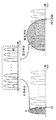
図1は本発明の概念を説明するための図である。図1を参照すれば、プログラム動作によってメモリセルは複数の閾値電圧状態、即ち、最下位状態(least state;LS)から最上位状態(most state;MS)の中でいずれか1つの閾値電圧分布を有する。以後、メモリセルに次のプログラム動作が要求される時、正常消去(normal erase)動作及び緊急消去(quick/weak/light/Psuedo/rough erase)動作の中でいずれか1つが選択的に実行できる。 FIG. 1 is a diagram for explaining the concept of the present invention. Referring to FIG. 1, a memory cell may have a threshold voltage distribution in a plurality of threshold voltage states, that is, from a least state (LS) to a most state (MS) according to a program operation. Have Thereafter, when the next program operation is requested for the memory cell, any one of a normal erase operation and an emergency erase (quick / weak / light / Psuedo / round erase) operation can be selectively performed. .
正常消去動作はプログラムされた状態を最下位状態LS或いはそれ以下の閾値電圧を有する消去状態Eにセットする。例えば、正常消去動作はメモリセルの閾値電圧を第1消去検証レベルERより大きくないようにする。ここで、第1消去検証レベルERは最下位状態LSを検証するレベルであり得る。
緊急消去動作はプログラム状態を第2消去検証レベルPERより大きくない閾値電圧を有する擬似消去状態(Psuedo E)にセットする。ここで、第2消去検証レベルPERは第1消去検証レベルERより大きい。第2消去検証レベルPERは緊急消去マージン(quick erase margin;QEM)と称され得る。ここで、緊急消去マージンQEMは、緊急消去動作以後に格納できるプログラム状態の個数を多くするか、或いは上書き(overwrite)をする場合、データの信頼性を向上させるために調節可能である。
A normal erase operation sets the programmed state to an erase state E having a threshold voltage of the lowest state LS or lower. For example, the normal erase operation prevents the threshold voltage of the memory cell from being higher than the first erase verification level ER. Here, the first erase verification level ER may be a level for verifying the lowest state LS.
The emergency erase operation sets the program state to a pseudo erase state (Psuedo E) having a threshold voltage not greater than the second erase verification level PER. Here, the second erase verification level PER is higher than the first erase verification level ER. The second erase verification level PER may be referred to as an emergency erase margin (QEM). Here, the emergency erase margin QEM can be adjusted in order to improve the reliability of data when the number of program states that can be stored after the emergency erase operation is increased or overwritten.
本発明はメモリセルの閾値電圧を擬似消去状態(Psuedo E)にセットする緊急消去動作を実行するか、或いは消去状態Eにセットする正常消去動作を実行することができる。
図2は擬似消去状態(Psuedo E)を利用するプログラム動作に対する第1実施形態を示す図である。説明を簡単にするために、以前に8つの状態が存在する3−ビットプログラム動作が実行されたと仮定する。
緊急消去動作によって、メモリセルは次のプログラム動作のための擬似消去状態(Psuedo E)になる。以後、擬似消去状態(Psuedo E)を利用する1−ビットプログラム動作が実行される。即ち、メモリセルは擬似消去状態(Psuedo E)及びプログラム状態Pの中でいずれか1つにプログラムされる。ここで、プログラム状態Pは第2消去検証レベルPERより高い閾値電圧分布を有する。
The present invention can execute an emergency erase operation for setting the threshold voltage of the memory cell to the pseudo erase state (Psuedo E) or a normal erase operation for setting to the erase state E.
FIG. 2 is a diagram showing a first embodiment for a program operation using a pseudo erase state (Psuedo E). For simplicity, assume that a 3-bit program operation has been performed that previously had 8 states.
Due to the emergency erase operation, the memory cell enters a pseudo erase state (Psuedo E) for the next program operation. Thereafter, a 1-bit program operation using the pseudo erase state (Psuedo E) is executed. That is, the memory cell is programmed to one of a pseudo erase state (Psuedo E) and a program state P. Here, the program state P has a threshold voltage distribution higher than the second erase verification level PER.
本発明は擬似消去状態(Psuedo E)を利用して1−ビットプログラム動作を実行できる。
図2で擬似消去状態(Psuedo E)は以前プログラム動作の状態が第2消去検証レベルPERより大きくない閾値電圧分布を有する。しかし、本発明が必ずしもこれに制限される必要はない。本発明の擬似消去状態(Psuedo E)はプログラム動作で所定の区間内に集まった閾値電圧分布を有することができる。
The present invention can execute a 1-bit program operation using a pseudo erase state (Psuedo E).
In FIG. 2, the pseudo erase state (Psuedo E) has a threshold voltage distribution in which the state of the previous program operation is not greater than the second erase verification level PER. However, the present invention is not necessarily limited to this. The pseudo erase state (Psuedo E) of the present invention may have a threshold voltage distribution gathered within a predetermined interval by a program operation.
図3は擬似消去状態(Psuedo E)を利用するプログラム動作に対する第2実施形態を示す図である。図3を参照すれば、擬似消去状態(Psuedo E)を利用するプログラム動作で、擬似消去状態(Psuedo E)は第2消去検証レベルPERより大きくなく、第3消去検証レベルPERLより小さくない閾値電圧を有する。ここで、第3消去検証レベルPERLは第1消去検証レベルERより大きく、第2消去検証レベルPERより小さい。
図2乃至図3は擬似消去状態(Psuedo E)を利用して1−ビットプログラム動作が実行される例を示す。しかし、本発明が必ずこれに制限される必要はない。本発明は擬似消去状態(Psuedo E)を利用して2−ビットプログラム動作を実行することができる。このために、緊急消去マージンQEMは1−ビットプログラム動作の時のそれよりさらに低くなる。
FIG. 3 is a diagram showing a second embodiment for a program operation using the pseudo erase state (Psuedo E). Referring to FIG. 3, in the program operation using the pseudo erase state (Psuedo E), the pseudo erase state (Psuedo E) is not greater than the second erase verify level PER and not less than the third erase verify level PERL. Have Here, the third erase verification level PERL is larger than the first erase verification level ER and smaller than the second erase verification level PER.
2 to 3 show an example in which a 1-bit program operation is executed using a pseudo erase state (Psuedo E). However, the present invention is not necessarily limited to this. The present invention can execute a 2-bit program operation using a pseudo erase state (Psuedo E). For this reason, the emergency erase margin QEM is further lower than that in the 1-bit program operation.
図4は擬似消去状態(Psuedo E)を利用するプログラム動作に対する第3実施形態を示す図である。図4を参照すれば、擬似消去状態(Psuedo E)を利用するプログラム動作でメモリセルは、擬似消去状態(Psuedo E)、第1プログラム状態P1、第2プログラム状態P2、及び第3プログラム状態P3の中でいずれか1つにプログラムされる。
また、本発明の擬似消去状態(Psuedo E)を利用するプログラム動作はエキストラ状態(extra state)を利用することもあり得る。ここで、エキストラ状態は以前プログラム動作で利用されなかった状態として、以前プログラム動作のプログラム状態より高い状態である。一方、エキストラ状態に対する詳細は、この出願の先行技術文献として記載された特許文献1で説明される。
FIG. 4 is a diagram showing a third embodiment for a program operation using the pseudo erase state (Psuedo E). Referring to FIG. 4, in a program operation using the pseudo erase state (Psuedo E), the memory cell is in a pseudo erase state (Psuedo E), a first program state P1, a second program state P2, and a third program state P3. Are programmed to any one of them.
Further, the program operation using the pseudo erase state (Psuedo E) of the present invention may use an extra state. Here, the extra state is a state that has not been used in the previous program operation, and is higher than the program state of the previous program operation. On the other hand, details regarding the extra state will be described in
図5は擬似消去状態(Psuedo E)を利用するプログラム動作に対する第4実施形態を示す図である。図5を参照すれば、擬似消去状態(Psuedo E)を利用するプログラム動作でメモリセルは、擬似消去状態(Psuedo E)、第1プログラム状態P1、第2プログラム状態P2、及び第3プログラム状態P3の中でいずれか1つにプログラムされる。ここで、第3プログラム状態P3はエキストラ状態を含む。
図5では1つのエキストラ状態が第3プログラム状態に包含されるが、本発明はこれに制限されない。本発明の擬似消去状態(Psuedo E)を利用するプログラム動作は少なくとも1つのエキストラ状態が少なくとも1つのプログラム状態に包含され得る。
FIG. 5 is a diagram showing a fourth embodiment for a program operation using the pseudo erase state (Psuedo E). Referring to FIG. 5, in a program operation using the pseudo erase state (Psuedo E), the memory cell is in a pseudo erase state (Psuedo E), a first program state P1, a second program state P2, and a third program state P3. Are programmed to any one of them. Here, the third program state P3 includes an extra state.
In FIG. 5, one extra state is included in the third program state, but the present invention is not limited to this. In the program operation using the pseudo erase state (Psuedo E) of the present invention, at least one extra state may be included in at least one program state.
また、本発明の擬似消去状態(Psuedo E)を利用するプログラム動作は多次元変調方式(multi dimension modulation scheme)のプログラム動作にも適用可能である。ここで、多次元変調方式は、格納されるデータ値をエンコーディングして連続した所定の個数のメモリセルにプログラムすることを言う。一方、多次元変調方式に対する詳細は本出願の出願人である三星電子から出願され、この出願の先行技術文献として記載された特許文献1で説明される。
In addition, the program operation using the pseudo erase state (Psuedo E) of the present invention can be applied to a program operation of a multi-dimension modulation scheme. Here, the multi-dimensional modulation method refers to encoding a stored data value and programming it into a predetermined number of memory cells. On the other hand, details of the multi-dimensional modulation system are described in
図6は本発明の擬似消去状態(Psuedo E)を利用するプログラム動作に対する第5実施形態を示す図である。図6を参照すれば、擬似消去状態(Psuedo E)を利用するプログラム動作でメモリセルは、多次元変調方式にしたがって擬似消去状態(Psuedo E)、第1プログラム状態P1、及び第2プログラム状態P2の中でいずれか1つにプログラムされる。 FIG. 6 is a diagram showing a fifth embodiment for a program operation using the pseudo erase state (Psuedo E) of the present invention. Referring to FIG. 6, in a program operation using the pseudo erase state (Psuedo E), the memory cell is subjected to a pseudo erase state (Psuedo E), a first program state P1, and a second program state P2 according to a multidimensional modulation method. Are programmed to any one of them.
図7は本発明の実施形態による不揮発性メモリ装置100を例示的に示すブロック図である。図7を参照すれば、不揮発性メモリ装置100はメモリセルアレイ110、アドレスデコーダ120、電圧発生回路130、入出力回路140、及び制御ロジック150を含む。
FIG. 7 is a block diagram illustrating a
本発明による不揮発性メモリ装置はNANDフラッシュメモリ(NAND Flash Memory)、垂直形NANDフラッシュメモリ(Vertical NAND、以下、‘VNAND’と称する)、NORフラッシュメモリ(NOR Flash Memory)、抵抗性RAM(Resistive Random Access Memory:RRAM(登録商標))、相変化メモリ(Phase−Change Memory:PRAM)、磁気抵抗メモリ(Magnetoresistive Random Access Memory:MRAM)、強誘電体メモリ(Ferroelectric Random Access Memory:FRAM(登録商標))、スピン注入磁化反転メモリ(Spin Transfer Torque Random Access Memory:STT−RAM)等であり得る。また、本発明の不揮発性メモリ装置100は3次元アレイ構造(three−dimensional array structure)で具現され得る。本発明の不揮発性メモリ装置100は電荷格納層が伝導性浮遊ゲートで構成されたフラッシュメモリ装置を含めて、電荷格納層が絶縁膜で構成されたチャージトラップ形フラッシュ(charge trap flash;CTF)にも全て適用できる。
The nonvolatile memory device according to the present invention includes a NAND flash memory, a vertical NAND flash memory (vertical NAND, hereinafter referred to as 'VNAND'), a NOR flash memory, and a resistive RAM (Resistive Random Random). Access Memory: RRAM (registered trademark), Phase-Change Memory (PRAM), Magnetoresistive Random Access Memory (MRAM), Ferroelectric Memory RandomFRAM (registered trademark) Spin transfer magnetization reversal memory (Spin Transf r Torque Random Access Memory: may be a STT-RAM) and the like. In addition, the
メモリセルアレイ110は複数のメモリブロック(BLK1〜BLKi、iは1より大きい整数)を含む。メモリブロックの各々は、ビットラインBLの各々に連結されたストリングを含む。ここで、ストリングは少なくとも1つのストリング選択トランジスタ、複数のメモリセル、少なくとも1つの接地選択トランジスタを含む。ストリング選択トランジスタはストリング選択ラインを通じて伝送される電圧によって駆動される。接地選択トランジスタは接地選択ラインを通じて伝送される電圧によって駆動される。メモリセルの各々は少なくとも1つのビットのデータを格納し、対応するワードラインWLへ伝送される電圧によって駆動される。
The
アドレスデコーダ120はアドレスに応答して複数のメモリブロックの中でいずれか1つを選択し、駆動に必要であるワードライン電圧(例えば、プログラム電圧、パス電圧、消去電圧、検証電圧、読出し電圧、読出しパス電圧等)を対応するワードラインへ伝送する。
電圧発生回路130は駆動に必要であるワードライン電圧を発生する。電圧発生回路130は高電圧発生器、低電圧発生器、及び/或いは負電圧発生器を含む。また、電圧発生回路130は消去動作のための消去電圧Veraseを発生する。消去電圧VeraseはメモリブロックBLK1〜BLKiの中で選択されたブロックのウェルへ印加される。
入出力回路140はプログラム動作で外部から入力されたデータを臨時的に格納した後に、選択されたページにプログラムし、読出し動作で読み出されるページからデータを読み出して臨時的に格納した後に外部へ出力する。入出力回路140はビットラインBLの各々に対応するページバッファを含む。
The
The
The input /
制御ロジック150は不揮発性メモリ装置100の全般的な動作を制御する。制御ロジック150は外部のメモリ制御器から提供される制御信号及び命令語を解釈し、解釈結果に応答してアドレスデコーダ120、電圧発生回路130及び入出力回路140を制御する。即ち、制御ロジック150は、駆動(例えば、プログラム/読出し/消去動作)に必要である電圧を発生するように電圧発生回路130を制御し、発生された電圧を対応するワードラインWLへ伝送するようにアドレスデコーダ120を制御し、プログラムされるページデータ及び読み出されたページデータを入出力するために入出力回路140を制御する。
The
また、制御ロジック150は正常消去モード(normal erase mode)にしたがって、消去動作を実行するか、或いは緊急消去モード(quick erase mode)にしたがって消去動作を実行する。正常消去モードではメモリセルの閾値電圧を消去状態Eにセットする。ここで、消去状態Eは最下位状態(図1参照、LS)或いはそれ以下である。また、緊急消去モードではメモリセルの閾値電圧を擬似消去状態(Psuedo E)にセットする。ここで、擬似消去状態(Psuedo E)は最上位状態(図1参照、MS)以下であり、第2消去検証レベル(図1参照、PER)以下である。
実施形態において、正常消去モード及び緊急消去モードの選択は外部のメモリ制御器から入力された消去モード選択命令によって決定され得る。他の実施形態において、正常消去モード及び緊急消去モードの選択は、不揮発性メモリ装置100で内部的に決定され得る。その他の実施形態において、正常消去モード及び緊急消去モードの選択は、製造者によって固定され得る。
In addition, the
In the embodiment, selection of the normal erase mode and the emergency erase mode may be determined by an erase mode selection command input from an external memory controller. In other embodiments, the selection of the normal erase mode and the emergency erase mode may be determined internally in the
本発明の不揮発性メモリ装置100では必要に応じて正常消去モード及び緊急消去モードの中のいずれか1つで消去動作を実行できる。
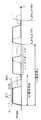
図8は図7に図示されたメモリブロックBLK1〜BLKiの中でいずれか1つのブロックBLKを例示的に示す図である。図8に図示されたメモリブロックBLKは基板上に垂直方向に形成される。図8を参照すれば、基板上に複数のワードラインカットの間には少なくとも1つの接地ストリングラインGSL、複数のワードラインWL、少なくとも1つのストリング選択ラインSSLが積層される。ここで、少なくとも1つのストリング選択ラインSSLはストリング選択ラインカットによって分離される。複数のピラーが少なくとも1つの接地ストリングライン基板GSL、複数のワードラインWL、少なくとも1つのストリング選択ラインSSLを貫通する。ここで、少なくとも1つの接地ストリングラインGSL、複数のワードラインWL、少なくとも1つのストリング選択ラインSSLは基板形態に具現される。また、複数のピラーの上部面には複数のビットラインBLが連結される。図8でメモリブロックはワードライン併合構造であるが、本発明がこれに制限される必要はない。
In the
FIG. 8 is a diagram exemplarily showing any one block BLK among the memory blocks BLK1 to BLKi shown in FIG. The memory block BLK illustrated in FIG. 8 is formed on the substrate in the vertical direction. Referring to FIG. 8, at least one ground string line GSL, a plurality of word lines WL, and at least one string selection line SSL are stacked on a substrate between a plurality of word line cuts. Here, at least one string selection line SSL is separated by a string selection line cut. A plurality of pillars penetrates at least one ground string line substrate GSL, a plurality of word lines WL, and at least one string selection line SSL. Here, the at least one ground string line GSL, the plurality of word lines WL, and the at least one string selection line SSL are implemented in a substrate form. A plurality of bit lines BL are connected to the upper surfaces of the plurality of pillars. In FIG. 8, the memory block has a word line merge structure, but the present invention is not limited to this.
一般的に3次元メモリ装置、電荷トラップフラッシュメモリ装置、或いはVNANDでは物性的/構造的特性のため、消去動作の時間(以下、消去時間)が長い。例えば、VNANDは大きいブロック/サブブロック単位に消去動作を実行するので、プラナメモリ装置と比較して長い消去時間を有する。このような長い消去時間は長くなった応答時間(response time)によって、システム性能(system performance)を低下させ得る。例えば、書込み動作の中で消去動作が実行される場合、長い消去時間のため、書込み動作の応答時間がタイムアウト(time−out)される可能性がある。
一方、本発明の不揮発性メモリ装置は、正常消去モード及び緊急消去モードの中のいずれか1つを選択して消去動作を実行できる。従って、本発明の不揮発性メモリ装置は応答時間が長くなることが予想される場合には緊急消去モードを通じて消去動作を実行することによって、消去時間を減少させ得る。その結果として、書込み動作の応答時間がタイムアウトされる可能性が減る。
Generally, a three-dimensional memory device, a charge trap flash memory device, or a VNAND has a long erase operation time (hereinafter, erase time) due to physical / structural characteristics. For example, since the VNAND performs an erase operation in units of large blocks / subblocks, it has a longer erase time than a planar memory device. Such a long erasure time may reduce system performance due to an increased response time. For example, when an erase operation is executed during a write operation, the response time of the write operation may time out due to the long erase time.
On the other hand, the nonvolatile memory device of the present invention can execute an erase operation by selecting one of the normal erase mode and the emergency erase mode. Therefore, the nonvolatile memory device of the present invention can reduce the erase time by executing the erase operation through the emergency erase mode when the response time is expected to be long. As a result, the possibility that the response time of the write operation is timed out is reduced.
本発明による不揮発性メモリ装置の緊急消去方法は正常消去動作で時間(或いは、サイクル)を変更することによって、具現され得る。
図9は本発明の実施形態による緊急消去方法に対する第1実施形態を示すタイミング図である。説明を簡単にするために図9では正常消去動作は2つのサイクルで構成されたとする。各サイクルはセットアップ区間、実行区間、回復区間、検証区間に区分される。実線はウェルへ印加される電圧、点線はワードラインへ印加される電圧を示す。図9を参照すれば、正常消去動作は2つのサイクルで構成され、セットアップ区間では消去動作のためにワードラインは接地電圧に、ビットラインとソースラインはフローティングされ、実行区間ではウェルへ消去電圧Veraseが印加され、回復区間ではウェル電圧とビットライン電圧が放電され、検証区間では消去動作が正しく実行されたか否かを判別するために第1検証レベル(図1参照、ER)で検証読出し動作が実行される。図9に図示しないが、サイクルが増加することによって、消去電圧Veraseは増加され得る。
The emergency erase method of the non-volatile memory device according to the present invention can be implemented by changing the time (or cycle) in a normal erase operation.
FIG. 9 is a timing diagram illustrating a first embodiment of an emergency erase method according to an embodiment of the present invention. In order to simplify the explanation, it is assumed in FIG. 9 that the normal erase operation is composed of two cycles. Each cycle is divided into a setup section, an execution section, a recovery section, and a verification section. A solid line indicates a voltage applied to the well, and a dotted line indicates a voltage applied to the word line. Referring to FIG. 9, the normal erase operation is composed of two cycles. In the setup period, the word line is set to the ground voltage for the erase operation, the bit line and the source line are floated, and the erase voltage Verase is supplied to the well in the execution period. Is applied, the well voltage and the bit line voltage are discharged in the recovery period, and the verification read operation is performed at the first verification level (see FIG. 1, ER) to determine whether the erase operation is correctly performed in the verification period. Executed. Although not shown in FIG. 9, the erase voltage Verase can be increased by increasing the cycle.
実施形態において、緊急消去動作は正常消去動作の中で一部サイクル(例えば、1つのサイクル)を実行する((1))。
他の実施形態において、緊急消去動作は正常消去動作の1つのサイクルの中で一部であり得る((2))。
整理すれば、本発明の緊急消去動作は、正常消去動作でサイクルの中で一部であるか、或いはいずれか1つのサイクルの一部であり得る。即ち、緊急消去動作は、正常消去動作の消去時間t_ers_normalより短い時間t_ers_quickの間に消去電圧Veraseをウェルへ印加することによって実行することができる。
In the embodiment, the emergency erase operation executes a partial cycle (for example, one cycle) in the normal erase operation ((1)).
In other embodiments, the emergency erase operation may be part of one cycle of a normal erase operation ((2)).
In summary, the emergency erase operation of the present invention can be part of a normal erase operation or part of any one cycle. That is, the emergency erase operation can be performed by applying the erase voltage Verase to the well during a time t_ers_quick shorter than the erase time t_ers_normal of the normal erase operation.
本発明の緊急消去方法は正常消去動作で消去電圧Veraseのレベルを変更することによって具現され得る。
図10は本発明の実施形態による緊急消去方法に対する第2実施形態を示すタイミング図である。図10を参照すれば、緊急消去方法は、正常消去動作のレベルVE_normalより低いレベルVE_quickを有する消去電圧Veraseを印加する。
実施形態において、緊急消去動作は低いレベルVE_quickを有する消去電圧Veraseを印加し、正常消去動作のようにすべてのサイクルを実行することであり得る((3))。
他の実施形態において、緊急消去動作は低いレベルVE_quickを有する消去電圧Veraseを印加し、一部サイクルを実行することであり得る((4))。
他の実施形態において、緊急消去動作は低いレベルVE_quickを有する消去電圧Veraseを印加し、1つのサイクルの中で一部を実行することであり得る((5))。
The emergency erase method of the present invention can be implemented by changing the level of the erase voltage Verase in a normal erase operation.
FIG. 10 is a timing diagram illustrating a second embodiment of an emergency erasing method according to an embodiment of the present invention. Referring to FIG. 10, in the emergency erase method, the erase voltage Verase having a level VE_quick lower than the level VE_normal of the normal erase operation is applied.
In an embodiment, the emergency erase operation may be to apply an erase voltage Verase having a low level VE_quick and execute all cycles like a normal erase operation ((3)).
In another embodiment, the emergency erase operation may be to apply an erase voltage Verase having a low level VE_quick and execute a partial cycle ((4)).
In another embodiment, the emergency erase operation may be to apply an erase voltage Verase having a low level VE_quick and execute a part in one cycle ((5)).
本発明の緊急消去方法は正常消去動作で消去電圧Veraseが印加される実行区間を減らすことによって具現され得る。
図11は本発明の実施形態による緊急消去方法に対する第3実施形態を示すタイミング図である。図11を参照すれば、緊急消去方法は、図9に図示された緊急消去方法と比較して消去電圧Veraseを印加する実行区間を減らす。即ち、緊急消去動作の1つのサイクルは正常消去動作の1つのサイクルより短い。
実施形態において、緊急消去動作は正常消去動作のように同一の回数のサイクルを実行する((6))。
他の実施形態において、緊急消去動作は正常消去動作のサイクル回数より少ない回数のサイクルを実行する((7))。
The emergency erasing method of the present invention can be implemented by reducing the execution period in which the erasing voltage Verase is applied in a normal erasing operation.
FIG. 11 is a timing diagram illustrating a third embodiment of an emergency erasing method according to an embodiment of the present invention. Referring to FIG. 11, the emergency erasing method reduces the execution period in which the erasing voltage Verase is applied as compared with the emergency erasing method illustrated in FIG. 9. That is, one cycle of the emergency erase operation is shorter than one cycle of the normal erase operation.
In the embodiment, the emergency erase operation executes the same number of cycles as the normal erase operation ((6)).
In another embodiment, the emergency erase operation executes fewer cycles than the normal erase operation ((7)).
本発明の緊急消去方法は、正常消去動作と比較して消去電圧Veraseのレベルを低くしながら、短いサイクルを実行することによって具現される。
図12は本発明の実施形態による緊急消去方法に対する第4実施形態を示すタイミング図である。図12を参照すれば、緊急消去動作は正常消去動作のレベルVE_normalと比較して低いレベルVE_quickを有する消去電圧Veraseを印加し、正常消去動作のサイクルより短いサイクルを実行する。
実施形態において、緊急消去動作は正常消去動作と同一な回数のサイクルを実行する((8))。
他の実施形態において、緊急消去動作は正常消去動作のサイクル回数より少ない回数のサイクルを実行する((9))。
The emergency erase method of the present invention is implemented by executing a short cycle while lowering the level of the erase voltage Verase as compared with the normal erase operation.
FIG. 12 is a timing diagram illustrating a fourth embodiment of the emergency erasing method according to an embodiment of the present invention. Referring to FIG. 12, in the emergency erase operation, an erase voltage Verase having a level VE_quick lower than the level VE_normal of the normal erase operation is applied, and a cycle shorter than the cycle of the normal erase operation is executed.
In the embodiment, the emergency erase operation executes the same number of cycles as the normal erase operation ((8)).
In another embodiment, the emergency erase operation executes fewer cycles than the normal erase operation ((9)).
図9乃至図12を参照すれば、本発明による緊急消去動作は、メモリセルを擬似消去状態(Psuedo E)にセットするために正常消去動作の時間、或いはレベルの多様な組合わせによって決定され得る。
図13は本発明の実施形態によるメモリシステムを示すブロック図である。図13を参照すれば、メモリシステム10は少なくとも1つの不揮発性メモリ装置100及びそれを制御するメモリ制御器200を含む。不揮発性メモリ装置100は図7で説明したのと同一である。メモリ制御器200は必要によって、不揮発性メモリ装置100の制御ロジック150を正常消去モードで動作させるか、或いは緊急消去モードで動作させるかを決定することができる。
Referring to FIGS. 9 to 12, the emergency erase operation according to the present invention can be determined by various combinations of time or level of normal erase operation to set the memory cell in a pseudo erase state (Psuedo E). .
FIG. 13 is a block diagram illustrating a memory system according to an embodiment of the present invention. Referring to FIG. 13, the
実施形態において、メモリ制御器200はホストの書込み要請に対する応答時間を予測し、予測された結果に基づいて緊急消去モードを選択することができる。例えば、メモリ制御器200は書込み要請の時、応答時間が長くなるマージ動作が必要であると判別される時、すぐに不揮発性メモリ装置100を緊急消去モードに動作するよう制御することができる。
実施形態において、メモリ制御器200はホストの使用者の要請に応答して緊急消去モードを選択することができる。例えば、使用者がより速い書込み動作を望む場合には、メモリ制御器200はこのような要請に応答して不揮発性メモリ装置100が緊急消去モードで動作するように制御することができる。
図14は本発明の実施形態によるメモリシステム10のプログラム方法を例示的に示すフローチャートである。図7乃至図14を参照すれば、プログラム方法は次の通りである。
In the embodiment, the
In the embodiment, the
FIG. 14 is a flowchart illustrating a method for programming the
メモリシステム10には外部のホストから書き込まれるデータ及びアドレス(例えば、論理アドレス)が入力される(S110)。メモリ制御器200は消去動作が必要であるか否かを判別する。例えば、データを書き込むプリブロックが存在しない時、データブロックを消去してプリブロックにセットする必要があり、このためにデータブロックに対する消去動作が実行されなければならない。例えば、メモリブロックの間にマージ動作の後、無効データ、或いはガーベッジ(garbage)を有するメモリブロックがプリブロックを必要とする時、消去動作が必要である(S120)。データブロックが消去される必要がなければ、S150段階が進行される。
Data and addresses (for example, logical addresses) written from an external host are input to the memory system 10 (S110). The
データブロックが消去される必要があれば、メモリ制御器200は緊急消去動作が必要であるか否かを判別する(S130)。もし、緊急消去動作が必要であれば、データブロックに対する緊急消去動作が実行される(S140)。これに対し、緊急消去動作が必要でなければ、データブロックに対する正常消去動作が実行される(S145)。データブロックに対する消去動作が完了した後に、アドレスに対応するメモリブロックに書き込まれるデータを格納するためのプログラム動作が実行される(S150)。したがって、本発明のプログラム動作が完了する。
If the data block needs to be erased, the
本発明のプログラム方法は、緊急消去動作が必要であるか否かを判別し、その結果にしたがって緊急消去動作を実行することによって、一般的なそれと比較してプログラム動作時間を短縮させ得る。
図15は本発明の実施形態によるメモリシステムのブロック管理方法に対する第1実施形態を示す図である。図15を参照すれば、メモリシステム10のメモリ制御器200は次の順序でメモリブロックを管理する。
According to the programming method of the present invention, it is possible to shorten the program operation time as compared with a general method by determining whether or not an emergency erase operation is necessary and executing the emergency erase operation according to the result.
FIG. 15 is a diagram illustrating a first embodiment of a block management method for a memory system according to an embodiment of the present invention. Referring to FIG. 15, the
処女状態のメモリブロックのページに最下位ビット(least significant bit;LSB)プログラム動作が実行される(S210)。以後、最下位ビットプログラムされたページに次のビットプログラム動作が実行され、このような方式で最上位ビット(most significant bit;MSB)プログラム動作が実行される(S220)。図15ではメモリブロックのページに最下位ビットLSBプログラム動作が先ず実行され、最上位ビットMSBプログラム動作が後に実行される。しかし、本発明がこれに制限される必要はない。反対に、メモリブロックのページに最上位ビットMSBプログラム動作が先に実行され、その後、最下位ビットLSBプログラム動作が実行されることもあり得る。 A least significant bit (LSB) program operation is performed on the page of the memory block in the virgin state (S210). Thereafter, the next bit program operation is performed on the page programmed with the least significant bit, and the most significant bit (MSB) program operation is performed in this manner (S220). In FIG. 15, the least significant bit LSB program operation is first performed on the page of the memory block, and the most significant bit MSB program operation is performed later. However, the present invention need not be limited to this. Conversely, the most significant bit MSB program operation may be performed on a page of the memory block first, followed by the least significant bit LSB program operation.
図15でマルチビットプログラム動作は1ビットずつ順に実行される。しかし、本発明のマルチビットプログラム動作は必ずしもこれに制限されない。本発明のマルチビットプログラム動作はマルチビットが一度に或いは同時にプログラムされることもある。
メモリブロックの複数のページが上述したようにプログラム動作が実行された後に、メモリブロックに格納されたデータが無効であると判別され得る。例えば、外部のホストに要請にしたがって格納されたデータが無効処理され得る。また、格納されたデータが物理的に他の位置に複写された後に、以前データを無効化処理することができる(S230)。
In FIG. 15, the multi-bit program operation is sequentially executed bit by bit. However, the multi-bit program operation of the present invention is not necessarily limited to this. The multi-bit program operation of the present invention may program multiple bits at once or simultaneously.
After a plurality of pages of the memory block have been programmed as described above, it can be determined that the data stored in the memory block is invalid. For example, data stored in accordance with a request from an external host can be invalidated. In addition, after the stored data is physically copied to another location, the previous data can be invalidated (S230).
この時、メモリ制御器200は無効化データを格納するメモリブロックに次のプログラム動作を実行するために緊急消去動作を実行する。ここで、緊急消去動作が実行されたメモリブロックに存在するメモリセルは擬似消去状態(Psuedo E)に位置する(S240)。擬似消去状態(Psuedo E)を利用してオーバーライト(overwrite)或いはプログラム動作が実行される(S250)。その後、メモリ制御器200は消去状態Eを利用する正常的なプログラム動作を実行するためにオーバーライト/プログラムされたメモリブロックに対して正常消去動作を実行し、S210段階へ進入する(S260)。
At this time, the
本発明によるメモリブロック管理方法は正常消去動作を実行する前に緊急消去動作を実行し、この時、発生した擬似消去状態(Psuedo E)を利用してオーバーライト/プログラム動作を実行できる。
本発明によるメモリブロック管理方法は、いずれか1つのメモリブロックに対する緊急消去動作を反復することもあり得る。
The memory block management method according to the present invention performs an emergency erase operation before executing a normal erase operation. At this time, an overwrite / program operation can be performed using the generated pseudo erase state (Psuedo E).
The memory block management method according to the present invention may repeat the emergency erase operation for any one memory block.
図16は本発明の実施形態によるメモリシステムのブロック管理方法に対する第2実施形態を示す図である。図16を参照すれば、メモリブロック管理方法は、図15に図示されたメモリブロック管理方法と比較してS255段階が追加される。
S255段階では、メモリ制御器200はメモリブロックに緊急消去動作を反復するための条件を満足するか否かを判別する。このような反復条件は、メモリブロックに関連した情報であり得る。例えば、反復条件はメモリブロックのプログラム/消去サイクル回数、ブロック消去比率等であり得る。緊急消去動作の反復条件を満足すれば、例えば、プログラム/消去サイクル回数或いはブロック消去比率が所定の値より小さければ、メモリブロックに対する緊急消去動作を反復するためにS230段階へ進入する。
FIG. 16 is a diagram illustrating a second embodiment of a block management method for a memory system according to an embodiment of the present invention. Referring to FIG. 16, in the memory block management method, step S255 is added as compared with the memory block management method illustrated in FIG.
In step S255, the
実施形態において、消去動作、プログラム動作、或いは読出し動作が成功的に実行された比率にしたがって、緊急消去動作の可否が決定され得る。例えば、このような比率が所定の値以上である時、緊急消去動作が実行できる。また、このような比率が所定の値以上である時、オーバーライト動作でメモリセル当たり幾つのビットがプログラムされるかが決定され得る。
実施形態において、緊急消去動作が反復される毎に、緊急消去マージンQEMは段々と低くなり得る。他の実施形態において、緊急消去動作が反復される毎に緊急消去マージンQEMは一定であり得る。
一方、緊急消去動作の反復条件を満足しなければ、正常的なプログラム動作のためにS260段階へ進入する。
In the embodiment, whether or not an emergency erase operation is possible may be determined according to a rate at which an erase operation, a program operation, or a read operation is successfully executed. For example, when such a ratio is greater than or equal to a predetermined value, an emergency erase operation can be performed. Also, when such a ratio is greater than or equal to a predetermined value, it can be determined how many bits are programmed per memory cell in an overwrite operation.
In an embodiment, the emergency erase margin QEM may be gradually lowered each time the emergency erase operation is repeated. In other embodiments, the emergency erase margin QEM may be constant each time the emergency erase operation is repeated.
On the other hand, if the repetition condition of the emergency erase operation is not satisfied, the process proceeds to step S260 for a normal program operation.
本発明によるメモリブロック管理方法は、メモリブロックの状態にしたがって反復的に緊急消去動作を実行できる。
図15及び図16では正常消去動作の前に緊急消去動作が実行される。しかし、本発明がこれに制限される必要はない。本発明の緊急消去動作は選択的に実行されることもできる。
The memory block management method according to the present invention can repeatedly execute an emergency erase operation according to the state of the memory block.
In FIGS. 15 and 16, the emergency erase operation is performed before the normal erase operation. However, the present invention need not be limited to this. The emergency erase operation of the present invention can also be selectively performed.
図17は本発明の実施形態によるメモリシステムのブロック管理方法に対する第3実施形態を示す図である。図17を参照すれば、メモリブロックの管理方法は次の通りである。
メモリブロックのページに最下位ビットLSBプログラム動作が先に実行され(S310)、以後に最上位ビットMSBプログラム動作が実行される(S320)。メモリブロックの複数のページに上述したようにプログラム動作が実行された後に、メモリブロックに格納されたデータが無効であると判別され得る(S330)。この時、メモリ制御器200は無効化されたデータを格納するメモリブロックに対して緊急消去動作を実行するか否かを判別する(S335)。例えば、ホストの要請が速い消去動作を要求する時、メモリ制御器200は緊急消去動作が実行されるように不揮発性メモリ装置100を制御することができる。
FIG. 17 is a diagram illustrating a third embodiment of a block management method for a memory system according to an embodiment of the present invention. Referring to FIG. 17, the memory block management method is as follows.
The least significant bit LSB program operation is first performed on the page of the memory block (S310), and then the most significant bit MSB program operation is performed (S320). After the program operation is performed on the plurality of pages of the memory block as described above, it may be determined that the data stored in the memory block is invalid (S330). At this time, the
もし、緊急消去動作を必要としなければ、S360段階へ進入する。一方、緊急消去動作が必要であれば、無効化データを格納するメモリブロックに次のプログラム動作を実行するために緊急消去動作を実行する。ここで、緊急消去動作が実行されたメモリブロックに存在するメモリセルは擬似消去状態(Psuedo E)に位置する(S340)。例えば、ホストから書込み要請が入力される時、データを不揮発性メモリ装置100の物理的位置に書き込むまでの時間(以下、書込み応答時間)が所定の値を超過したと予測される時、メモリ制御器200は緊急消去動作を実行するように不揮発性メモリ装置100を制御する。ここで、書込み応答時間にはマージ動作時間或いは消去時間が包含される。
If the emergency erase operation is not required, the process proceeds to step S360. On the other hand, if the emergency erase operation is necessary, the emergency erase operation is executed to execute the next program operation on the memory block storing the invalidation data. Here, the memory cells existing in the memory block on which the emergency erase operation has been executed are positioned in the pseudo erase state (Psuedo E) (S340). For example, when a write request is input from the host, when it is predicted that the time until data is written to the physical location of the nonvolatile memory device 100 (hereinafter, write response time) exceeds a predetermined value, the memory control is performed. The
実施形態において、消去時間は、プリブロックの個数、ブロック消去比率BER、プログラム/消去サイクル、データリテンション時間(data retention time)、動作温度の中で少なくとも1つを利用して予測することができる。ここで、ブロック消去比率BERが所定の値以上である時、消去時間が長くなるので、緊急消去動作が実行される。また、ブロック消去比率BERが所定の値以上である時、マルチビットオーバーライトが難しいことがあり得るので、オーバーライト動作の時、幾つかのビットにプログラム動作が実行されるかが決定されなければならない。 In the embodiment, the erase time may be estimated using at least one of the number of pre-blocks, the block erase ratio BER, the program / erase cycle, the data retention time, and the operating temperature. Here, when the block erase ratio BER is equal to or greater than a predetermined value, the erase time becomes longer, and therefore the emergency erase operation is executed. Further, when the block erase ratio BER is equal to or higher than a predetermined value, multi-bit overwriting may be difficult. Therefore, it is not determined whether a program operation is executed for some bits during the overwriting operation. Don't be.
以後、擬似消去状態(Psuedo E)を利用してオーバーライト(overwrite)或いはプログラム動作が実行される(S350)。その後、メモリ制御器200は消去状態Eを利用する正常的なプログラム動作を実行するためにメモリブロックに対して正常消去動作を実行し、S310段階へ進入する(S360)。
本発明のメモリブロック管理方法は予測された書込み応答時間によって、メモリブロックに緊急消去動作を実行できる。
図15乃至図17では1つの物理ページに複数の論理ページが順次的にプログラムされる場合を開示する。しかし、本発明がこれのみに制限されない。本発明は1つの物理ページに複数の論理ページが一度にプログラムされる場合にも適用可能である。即ち、本発明はオンチップバッファプログラム(on−chip buffered program;以下、‘OBP’)にも適用可能である。
Thereafter, an overwrite or program operation is performed using the pseudo erase state (Psuedo E) (S350). Thereafter, the
The memory block management method of the present invention can execute an emergency erase operation on the memory block according to the predicted write response time.
15 to 17 disclose a case where a plurality of logical pages are sequentially programmed in one physical page. However, the present invention is not limited to this. The present invention is also applicable to the case where a plurality of logical pages are programmed at one time on one physical page. That is, the present invention can also be applied to an on-chip buffered program (hereinafter referred to as “OBP”).
図18は本発明の実施形態によるOBPを使用するメモリシステムを例示的に示すブロック図である。図18を参照すれば、メモリシステム20は少なくとも1つの不揮発性メモリ装置300及びそれを制御するメモリ制御器400を含む。
不揮発性メモリ装置300はページデータを1つのメモリセル当たり1−ビットで格納するシングルレベルセル領域311、シングルレベルセル領域311に格納された複数のページデータを1つのページに一度に格納する(或いは、メモリセル当たりマルチ−ビットで格納する)マルチレベルセル領域312、及び制御ロジック350を含む。シングルレベルセル領域311及びマルチレベルセル領域312の各々は複数のメモリブロックを含む。制御ロジック350は正常消去動作を実行する正常消去モード及び緊急消去動作を実行する緊急消去モードを有する。メモリ制御器400はシングルレベルセル領域311に格納されたページデータを読出し、読み出されたページデータのエラーを訂正するエラー訂正回路420を包含することができる。
FIG. 18 is a block diagram illustrating a memory system using OBP according to an embodiment of the present invention. Referring to FIG. 18, the
The
本発明のメモリシステム20はシングルレベルセル領域311のメモリブロックに対して緊急消去動作を実行できる。
他の実施形態において、本発明のメモリシステム20はシングルレベルセル領域311及びマルチレベルセル領域312の中でいずれか1つに選択的に正常消去動作或いは緊急消去動作を実行することができる。
The
In another embodiment, the
図19は図18に図示されたシングルレベルセル領域311のメモリブロックの閾値電圧変化過程を例示的に示す図である。図19を参照すれば、シングルレベルセル領域311のメモリブロックの閾値電圧状態変化は次の通りである。
最初に消去状態Eを利用する1−ビットプログラム動作が実行される。これによってメモリブロックのメモリセルは消去状態Eとプログラム状態P0の中でいずれか1つにプログラムされる。以後、メモリブロックに消去動作が必要であれば、緊急消去動作が実行される。図19に示したように、以前プログラム動作のプログラム状態P0は擬似消去状態(Psuedo E)になるように緊急消去動作を通じてメモリセルの閾値電圧が低くなる。緊急消去動作が実行された後、擬似消去状態(Psuedo E)を利用して1−ビットプログラム動作が実行される。即ち、メモリブロックのメモリセルは擬似消去状態(Psuedo E)或いはプログラム状態Pの中でいずれか1つにプログラムされる。
FIG. 19 is a diagram illustrating a threshold voltage changing process of the memory block of the single
First, a 1-bit program operation using the erase state E is executed. As a result, the memory cell of the memory block is programmed to one of the erase state E and the program state P0. Thereafter, if an erase operation is necessary for the memory block, an emergency erase operation is performed. As shown in FIG. 19, the threshold voltage of the memory cell is lowered through the emergency erase operation so that the program state P0 of the previous program operation becomes a pseudo erase state (Psuedo E). After the emergency erase operation is executed, a 1-bit program operation is executed using the pseudo erase state (Psuedo E). That is, the memory cells of the memory block are programmed to one of the pseudo erase state (Psuedo E) and the program state P.
図20は図18に図示されたメモリシステム20のメモリブロック管理方法を例示的に示す図である。図20を参照すれば、メモリシステム20のメモリブロック管理方法は次の通りである。
優先的に、メモリブロックのシングルレベルセル領域311のページにプログラム動作が実行される(S410)。メモリブロックに格納されたデータが無効であると判別され得る(S420)。この時、メモリ制御器400は無効化されたデータを格納するメモリブロックのプログラム/消去サイクル或いはブロック消去比率が所定の値より下であるか否かを判別する(S430)。ここで、プログラム/消去サイクル或いはブロック消去比率はブロックの状態条件になることができる。一方、ブロックの状態条件は、消去動作、プログラム動作、或いは読出し動作が成功的に実行された比率であることもあり得る。
FIG. 20 is a diagram illustrating a memory block management method of the
Preferentially, the program operation is performed on the page of the single
もし、プログラム/消去サイクル或いはブロック消去比率が所定の値未満ではない時、S460段階へ進入する。一方、プログラム/消去サイクル或いはブロック消去比率が所定の値未満である時、無効化データを格納するメモリブロックに次のプログラム動作を実行するために緊急消去動作を実行する。ここで、緊急消去動作が実行されたメモリブロックに存在するメモリセルは擬似消去状態(Psuedo E)に位置する(S440)。 If the program / erase cycle or the block erase ratio is not less than a predetermined value, the process proceeds to step S460. On the other hand, when the program / erase cycle or the block erase ratio is less than a predetermined value, an emergency erase operation is performed to execute the next program operation on the memory block storing the invalidated data. Here, the memory cells existing in the memory block on which the emergency erase operation has been executed are positioned in the pseudo erase state (Psuedo E) (S440).
その後、擬似消去状態(Psuedo E)を利用してオーバーライト(overwrite)或いはプログラム動作が実行される(S450)。ここで、オーバーライト或いはプログラム動作はメモリセル当たり1−ビットプログラム動作である。以後に、メモリ制御器400は消去状態Eを利用する正常的な1−ビットプログラム動作を実行するためにメモリブロックに対して正常消去動作を実行し、S410段階へ進入する(S460)。
Thereafter, an overwrite or program operation is executed using the pseudo erase state (Psuedo E) (S450). Here, the overwrite or program operation is a 1-bit program operation per memory cell. Thereafter, the
本発明のメモリブロック管理方法は、メモリブロックの状態を考慮して緊急消去動作を実行するか否かを決定する。
図18で1つの不揮発性メモリ装置300はシングルレベルセル領域311及びマルチレベルセル領域312を含む。しかし、本発明が必ずしもこれに制限される必要はない。本発明はページデータをバッファリングするためのシングルレベルセル領域311のみを有する別の不揮発性メモリ装置を具備することもある。
The memory block management method of the present invention determines whether or not to perform an emergency erase operation in consideration of the state of the memory block.
In FIG. 18, one
図21は本発明のその他の実施形態によるOBPを使用するメモリシステムを例示的に示すブロック図である。図21を参照すれば、メモリシステム30は第1不揮発性メモリ装置500−1、第2不揮発性メモリ装置500−2、及びメモリ制御器600を含む。第1不揮発性メモリ装置500−1はシングルレベルセル領域511及び制御ロジック550−1を含む。第2不揮発性メモリ装置500−2はマルチレベルセル領域512を含む。
本発明のメモリシステム30は、ページデータを第1不揮発性メモリ装置500−1のシングルレベルセル領域511にバッファリングして置いた後に、第2不揮発性メモリ装置500−2のマルチレベルセル領域512にプログラムさせる。ここで、シングルレベルセル領域511は緊急消去モード或いは正常消去モードにしたがって消去されるメモリブロックを含む。
FIG. 21 is a block diagram illustrating a memory system using OBP according to another embodiment of the present invention. Referring to FIG. 21, the
The
図22は本発明の実施形態によるメモリシステムの書込み動作を例示的に示すフローチャートである。図22を参照すれば、メモリシステムの書込み動作は次の通りである。
ホストからメモリシステムに書込み要請が入力される。この時、データ及びアドレス(論理アドレス)が入力される(S510)。メモリシステムは書込み速度の増加が必要であるか否かを判別する(S520)。ここで、書込み速度の増加に対する判別動作は、ホストの要請によって決定され得る。実施形態において、書込み速度の増加に対する判別動作は、入力されたデータ関連情報にしたがって決定され得る。例えば、大容量データである場合、速い書込み速度が必要であると判別される。
FIG. 22 is a flowchart illustrating a write operation of the memory system according to the embodiment of the present invention. Referring to FIG. 22, the write operation of the memory system is as follows.
A write request is input from the host to the memory system. At this time, data and an address (logical address) are input (S510). The memory system determines whether or not the write speed needs to be increased (S520). Here, the determination operation with respect to the increase in the writing speed may be determined according to a request from the host. In the embodiment, the determination operation for the increase of the writing speed may be determined according to the input data related information. For example, in the case of large-capacity data, it is determined that a fast writing speed is necessary.
もし、書込み速度を増加させる必要があれば、メモリ制御器は緊急消去モードを設定するための命令語を不揮発性メモリ装置へ伝送する(S530)。不揮発性メモリ装置は伝送された命令語にしたがって緊急消去モードを設定し、以後消去命令に応答して緊急消去動作を実行する。
一方、書込み速度を増加させる必要がなければ、メモリ制御器は正常消去モードを設定するための命令語を不揮発性メモリ装置へ伝送する(S535)。不揮発性メモリ装置は伝送された命令語にしたがって正常消去モードを設定し、以後消去命令に応答して緊急消去動作を実行する。しかし、本発明のモード設定はこれに制限されない。正常消去モードの設定は別の設定過程無しでデフォルト値に決定することができる。
If it is necessary to increase the writing speed, the memory controller transmits a command word for setting the emergency erase mode to the nonvolatile memory device (S530). The nonvolatile memory device sets an emergency erase mode according to the transmitted command word, and thereafter executes an emergency erase operation in response to the erase command.
On the other hand, if it is not necessary to increase the writing speed, the memory controller transmits a command word for setting the normal erase mode to the nonvolatile memory device (S535). The non-volatile memory device sets a normal erase mode according to the transmitted command word, and thereafter executes an emergency erase operation in response to the erase command. However, the mode setting of the present invention is not limited to this. The normal erase mode can be set to a default value without a separate setting process.
以後、メモリ制御器は設定された消去モードで入力されたデータを不揮発性メモリ装置にプログラムするように制御する(S540)。
本発明によるメモリシステムの書込み方法は書込み速度を増加させるか否かを判別し、その結果にしたがって緊急消去動作の可否を決定する。
上述したように本発明の緊急消去動作はメモリセルを最上位状態(図1参照、MS)下の擬似消去状態(Psuedo E)にセットすることである。しかし、緊急消去動作は必ずしもこれに制限されない。緊急消去動作は、別の消去動作を実行せず、以前プログラム状態をそのまま擬似消去状態(Psuedo E)として利用することもできる。
Thereafter, the memory controller controls the non-volatile memory device to program the input data in the set erase mode (S540).
The write method of the memory system according to the present invention determines whether or not to increase the write speed, and determines whether or not an emergency erase operation is possible according to the result.
As described above, the emergency erase operation of the present invention is to set the memory cell in the pseudo erase state (Psuedo E) below the uppermost state (see FIG. 1, MS). However, the emergency erase operation is not necessarily limited to this. In the emergency erase operation, another erase operation is not executed, and the previous program state can be used as it is as a pseudo erase state (Psuedo E).
一方、本発明の緊急消去動作は、擬似消去状態(Psuedo E)にセットするものに制限されない。本発明の正常消去動作よりむしろ高い消去電圧或いは制限された時間内に多サイクルを印加することで具現されることもあり得る。
本発明は多様な装置に応用可能である。
On the other hand, the emergency erase operation of the present invention is not limited to the one set in the pseudo erase state (Psuedo E). The present invention may be realized by applying multiple cycles within a high erase voltage or a limited time rather than the normal erase operation of the present invention.
The present invention can be applied to various apparatuses.
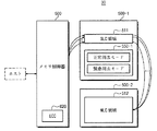
図23は本発明によるメモリシステムを例示的に示すブロック図である。図23を参照すれば、メモリシステム1000は少なくとも1つの不揮発性メモリ装置1100及びメモリ制御器1200を含む。メモリシステム1000は、図1乃至図22に上述されたように緊急消去動作を実行できる。
不揮発性メモリ装置1100は外部から高電圧Vppがオプション的に提供され得る。メモリ制御器1200は複数のチャンネルを通じて不揮発性メモリ装置1100に連結される。メモリ制御器1200は少なくとも1つの中央処理装置1210、バッファメモリ1220、エラー訂正回路1230、ROM1240、ホストインターフェイス1250、及びメモリインターフェイス1260を含む。メモリ制御器1200はデータをランダム化させるか、或いはデランダム化させるランダム化回路(図示せず)をさらに包含できる。本発明のメモリシステム1000はPPN(Perfect Page New)に適用可能である。不揮発性メモリ装置1110は、外部の高電圧を選択的に受信することができる。
FIG. 23 is a block diagram illustrating a memory system according to the present invention. Referring to FIG. 23, the
The
メモリ制御器1200は不揮発性メモリ装置1100のプログラム動作がフェイルされるか、或いはプログラム動作の信頼性が要求される時、データ復旧命令を発生し、発生されたデータ復旧命令を不揮発性メモリ装置1100へ伝送することができる。
メモリ制御器1200はエラー訂正コード(error correction code;ECC)にしたがってデータのエラーを訂正するエラー訂正回路1230を含む。エラー訂正回路1230は書込み動作でプログラムされるデータのエラー訂正コード値を計算し、読出し動作で読み出されたデータをエラー訂正コード値に基づいてエラー訂正できる。メモリ制御器1200はデータ復旧動作で復旧されたデータを他の物理的なページにプログラムさせるように不揮発性メモリ装置1100へプログラム命令を伝送することができる。
本発明によるメモリシステム1000は緊急消去動作を実行することによって、速い書込み速度が要求される大容量のデータを高速に格納できる。
The
The
The
図24は本発明によるメモリカードを例示的に示すブロック図である。図24を参照すれば、メモリカード2000は少なくとも1つのフラッシュメモリ装置2100、バッファメモリ装置2200、及びそれらを制御するメモリ制御器2300を含む。メモリカード2000は、図1乃至図22で上述したように緊急消去動作を実行できる。
フラッシュメモリ装置2100は外部高電圧Vppをオプション的に受信することができる。バッファメモリ装置2200はメモリカード2000の動作の際に生成されるデータを臨時的に格納するための装置である。バッファメモリ装置2200はDRAM或いはSRAM等で具現され得る。メモリ制御器2300は複数のチャンネルを通じてフラッシュメモリ装置2100に連結される。メモリ制御器2300はホスト及びフラッシュメモリ装置2100の間に連結される。ホストからの要請に応答して、メモリ制御器2300はフラッシュメモリ装置2100をアクセスする。
FIG. 24 is a block diagram illustrating a memory card according to the present invention. Referring to FIG. 24, the
The
メモリ制御器2300は少なくとも1つのマイクロプロセッサ2310、ホストインターフェイス2320、フラッシュインターフェイス2330を含む。少なくとも1つのマイクロプロセッサ2310はファームウェア(firmware)を動作するように具現される。ホストインターフェイス2320はホストとメモリカード2000との間にデータ交換を実行するためのカードプロトコル(例えば、SD/MMC)を通じてホストとインターフェイシングする。
本発明のメモリカード2000はマルチメディアカード(Multimedia Card:MMC)、保安デジタル(Security Digital:SD)、miniSD、USBを利用するメモリスティック(Memory Stick)、スマートメディア(Smart Media(登録商標))、トランスフラッシュ(TransFlash)カード等に適用可能である。
The
The
図25は本発明によるmoviNANDを例示的に示すブロック図である。図25を参照すれば、moviNAND3000は少なくとも1つのNANDフラッシュメモリ装置3100及び制御器3200を包含することができる。moviNAND3000はMMC4.4(言い換えれば、eMMC)規格を支援する。moviNAND3000は、図1乃至図22で上述したように緊急消去動作を実行できる。
FIG. 25 is a block diagram illustrating a movieNAND according to the present invention. Referring to FIG. 25, the
NANDフラッシュメモリ装置3100はSDR(Sing Data Rate)NAND或いはDDR(Double Data Rate)NANDであり得る。実施形態において、NANDフラッシュメモリ装置3100は単品のNANDフラッシュメモリ装置を含むことができる。ここで、単品のNANDフラッシュメモリ装置は1つのパッケージ(例えば、FBGA、Fine−pitch Ball Grid Array)に積層され得る。メモリ制御器3200は複数のチャンネルを通じてフラッシュメモリ装置3100に連結される。制御器3200は少なくとも1つの制御器コア3210、ホストインターフェイス3250、及びNANDインターフェイス3260を含む。少なくとも1つの制御器コア3210はmoviNAND3000の全般的な動作を制御する。ホストインターフェイス3250は制御器3210とホストのインターフェイシングを実行する。NANDインターフェイス3260はNANDフラッシュメモリ装置3100と制御器3200のインターフェイシングを実行する。実施形態において、ホストインターフェイス3250は並列インターフェイス(例えば、MMCインターフェイス)であり得る。他の実施形態において、moviNAND3000のホストインターフェイス3250は直列インターフェイス(例えば、UHS−II、UFSインターフェイス)であり得る。
The NAND
moviNAND3000はホストから電源電圧Vcc、Vccqを受信する。ここで、第1電源電圧(Vcc:3.3V)はNANDフラッシュメモリ装置3100及びNANDインターフェイス3230へ提供され、第2電源電圧(Vccq:1.8V/3.3V)は制御器3200へ提供される。実施形態において、moviNAND3000は外部高電圧Vppがオプション的に提供され得る。
本発明によるmoviNAND3000は大容量のデータを格納するのに有利であることのみでなく、向上された書込み動作特性を有する。本発明の実施形態によるmoviNAND3000は小型及び低電力が要求されるモバイル製品(例えば、ギャラクシーS(登録商標)、ギャラクシーノート(登録商標)、ギャラクシータブ(登録商標)、アイフォン(登録商標)、アイパッド(登録商標)等)に応用可能である。
The
The
図26は本発明によるSSDを例示的に示すブロック図である。図26を参照すれば、SSD4000は複数のフラッシュメモリ装置4100及びSSD制御器4200を含む。SSD4000は、図1乃至図22に上述されたように緊急消去動作を実行できる。
フラッシュメモリ装置4100はオプション的に外部高電圧Vppを提供されるように具現され得る。SSD制御器4200は複数のチャンネルCH1〜CH4を通じてフラッシュメモリ装置4100に連結される。SSD制御器4200は少なくとも1つの中央処理装置4210、バッファメモリ4220、ホストインターフェイス4250、及びフラッシュインターフェイス4260を含む。
本発明によるSSD4000はデータの信頼性を向上させるプログラム動作を実行する。一方、SSD4000に対するさらなる詳細は本出願の出願人である三星電子から出願し、先行技術文献として記載された特許文献2乃至6で説明される。
FIG. 26 is a block diagram illustrating an SSD according to the present invention. Referring to FIG. 26, the
The
The
図27は本発明による通信装置を例示的に示すブロック図である。図27を参照すれば、モバイル装置8000は通信ユニット8100、制御器8200、メモリユニット8300、ディスプレイユニット8400、タッチスクリーンユニット8500、及びオーディオユニット8600を含む。メモリユニット8300は少なくとも1つのDRAM8310、少なくとも1つのOneNAND8320、及び少なくとも1つのmoviNAND8330を含む。OneNAND8320及びMoviNAND8330の中で少なくとも1つは図23に図示されたメモリシステム1000と同一な構成及び動作を有するように具現される。
FIG. 27 is a block diagram illustrating a communication apparatus according to the present invention. Referring to FIG. 27, the
図28は本発明によるスマートTVシステムを例示的に示すブロック図である。図28を参照すれば、スマートTVシステム9000はスマートTV9100、レヴュー9200、セットトップボックス9300、無線共有器9400、キーパッド9500、及びスマートフォン9600を含む。スマートTV9100と無線共有器9400との間に無線通信が実行される。スマートTV9100は開放形プラットホームであるGoogle陣営のレヴュー(Revue、9200)を具備することによって、インターネットに接続が可能である。スマートTV9100はセットトップボックス9300を通じてケーブル放送及び衛星放送を視聴することができる。スマートTVはキーパッド9500の制御或いはスマートフォン9600の制御にしたがって運用され得る。本発明のスマートTV9100は図23に図示されたメモリシステム1000を包含することができる。
FIG. 28 is a block diagram illustrating a smart TV system according to the present invention. Referring to FIG. 28, the
本発明の実施形態によるメモリシステム或いは格納装置は多様な形態のパッケージを利用して実装され得る。実施形態において、本発明の実施形態によるメモリシステム或いは格納装置はPoP(Package on Package)、Ball grid arrays(BGAs)、Chip scale packages(CSPs)、Plastic Leaded Chip Carrier(PLCC)、Plastic Dual In−Line Package(PDIP)、Die in Waffle Pack、Die in Wafer Form、Chip On Board(COB)、Ceramic Dual In−Line Package(CERDIP)、Plastic Metric Quad Flat Pack(MQFP)、Thin Quad Flatpack(TQFP)、Small Outline(SOIC)、Shrink Small Outline Package(SSOP)、Thin Small Outline(TSOP)、Thin Quad Flatpack(TQFP)、System In Package(SIP)、Multi Chip Package(MCP)、Wafer−level Fabricated Package(WFP)、Wafer−Level Processed Stack Package(WSP)、等のようなパッケージを利用して実装され得る。 The memory system or the storage device according to the embodiment of the present invention may be implemented using various types of packages. In the embodiment, the memory system or the storage device according to the embodiment of the present invention includes PoP (Package on Package), Ball grid arrays (BGAs), Chip scale packages (CSPs), Plastic Leaded Chip Carrier (PLCC), Plastic In D Package (PDIP), Die in Waffle Pack, Die in Wafer Form, Chip On Board (COB), Ceramic Dual In-Line Package (CERDIP), Plastic Metric Quad P (SOIC), Shrink Small Outline Package (SSOP), Thin Small Outline (TSOP), Thin Quad Flatpack (TQFP), System In Package (FIP), MultiChip Package (FIP), Multi Chip Package (FIP), Multi Chip Package (MCP). -Can be implemented using a package such as Level Processed Stack Package (WSP).
一方、本発明の詳細な説明では具体的な実施形態に関して説明したが、本発明の範囲で逸脱しない範囲内で様々に変形できる。したがって本発明の範囲は上述した実施形態に限定されてはならないし、後述する特許請求の範囲のみでなくこの発明の特許請求の範囲と均等なものによって定められる。 On the other hand, although the specific embodiments have been described in the detailed description of the present invention, various modifications can be made without departing from the scope of the present invention. Therefore, the scope of the present invention should not be limited to the above-described embodiments, and is defined not only by the claims described below but also by the equivalents of the claims of the present invention.
ER・・・第1消去検証レベル
PER・・・第2消去検証レベル
QEM・・・緊急消去マージン
Psuedo E・・・擬似消去状態
100・・・不揮発性メモリ装置
110・・・メモリセルアレイ
120・・・アドレスデコーダ
130・・・電圧発生回路
140・・・入出力回路
150・・・制御ロジック
200・・・メモリ制御器
10、20、30・・・メモリシステム
Verase・・・消去電圧
311・・・シングルレベルセル領域
312・・・マルチレベルセル領域
ER ... first erase verification level PER ... second erase verification level QEM ... emergency erase margin Psuedo E ... pseudo erase
Claims (10)
消去モードを設定する段階と、
前記設定された消去モードにしたがって正常消去動作及び緊急消去動作の中でいずれか1つを実行する段階と、を含み、
前記正常消去動作は、メモリブロックに含まれるメモリセルの閾値電圧を第1消去検証レベルより低い消去状態にセットし、
前記緊急消去動作は、前記メモリブロックに含まれるメモリセルの閾値電圧を第2消去検証レベルより低い擬似消去状態にセットし、
前記第2消去検証レベルは前記第1消去検証レベルより高く、
ここで前記緊急消去動作は、消去動作、プログラム動作、又は読出し動作のいずれかの成功率に基づいて選択され、
前記緊急消去動作を実行する時、前記第2消去検証レベルに対応する緊急消去マージンを前記成功率に基づいて決定する段階をさらに含む消去方法。 In an erasing method of a nonvolatile memory device,
Set the erase mode,
Performing any one of a normal erase operation and an emergency erase operation according to the set erase mode,
In the normal erase operation , the threshold voltage of the memory cell included in the memory block is set to an erase state lower than the first erase verification level,
The emergency erase operation sets a threshold voltage of a memory cell included in the memory block to a pseudo erase state lower than a second erase verification level;
The second erase verification level is higher than the first erase verification level;
Here, the emergency erase operation is selected based on the success rate of any of the erase operation, the program operation, or the read operation,
An erase method further comprising: determining an emergency erase margin corresponding to the second erase verification level based on the success rate when performing the emergency erase operation.
消去されるメモリブロックのワードラインにバイアスを設定する段階と、
消去されるメモリブロックのビットライン及び消去されないワードラインをフローティングさせるバイアスの設定段階と、
前記メモリブロックのウェルへ消去電圧を印加する実行段階と、
前記ビットラインの電圧、前記ワードラインの電圧、及び前記ウェルの電圧を放電するリカバリ段階と、
前記メモリブロックのメモリセルの閾値電圧が前記消去状態に存在するか否かを判別す
る検証段階と、を含む請求項4に記載の消去方法。 Each of the plurality of cycles is
Setting a bias on the word line of the memory block to be erased;
A bias setting stage for floating the bit lines of the memory block to be erased and the word lines not to be erased;
Performing an erase voltage on the well of the memory block;
A recovery step of discharging the voltage of the bit line, the voltage of the word line, and the voltage of the well;
The erasing method according to claim 4, further comprising: a verifying step of determining whether a threshold voltage of a memory cell of the memory block exists in the erased state.
前記少なくとも1つの不揮発性メモリ装置を制御するメモリ制御器と、を含み、
前記少なくとも1つの不揮発性メモリ装置は、
ページデータをメモリセル当たり1−ビットプログラムする複数の第1メモリセルを有する第1メモリブロックを含む第1メモリセルアレイと、
前記第1メモリセルアレイの複数のページデータをいずれか1つのページにマルチ−ビットプログラムする複数の第2メモリセルを有する第2メモリブロックを含む第2メモリセルアレイと、
前記第1メモリブロックを第1消去モード及び第2消去モードの中のいずれか1つで消去し、前記第2メモリブロックを前記第1消去モードで消去する制御ロジックと、を含み、
前記第1消去モードは前記第1メモリセル或いは前記第2メモリセルを消去状態にセットし、
前記第2消去モードは前記第1メモリセルを擬似消去状態にセットし、
前記消去状態は第1消去検証レベルより低く、
前記擬似消去状態は第2消去検証レベルより低く、
前記第2消去検証レベルは前記第1消去検証レベルより高く、
前記第1及び第2消去モードは前記第1及び第2メモリブロックの状態にしたがって決定され、
ここで前記第2消去モードは前記第1メモリブロックの消去動作、プログラム動作、又は読出し動作のいずれかの成功率に基づいて選択され、前記第1メモリセルの各々は前記消去状態又は前記擬似消去状態に基づいて1−ビットプログラムされるメモリシステム。
At least one non-volatile memory device;
A memory controller for controlling the at least one non-volatile memory device;
The at least one non-volatile memory device includes:
A first memory cell array including a first memory block having a plurality of first memory cells that program 1-bit page data per memory cell;
A second memory cell array including a second memory block having a plurality of second memory cells for multi-bit programming a plurality of page data of the first memory cell array into any one page;
Control logic for erasing the first memory block in one of a first erase mode and a second erase mode, and erasing the second memory block in the first erase mode,
The first erase mode sets the first memory cell or the second memory cell to an erased state,
The second erase mode sets the first memory cell to a pseudo erase state,
The erase state is lower than a first erase verification level;
The pseudo erase state is lower than a second erase verification level;
The second erase verification level is higher than the first erase verification level;
The first and second erase modes are determined according to states of the first and second memory blocks ;
Here, the second erase mode is selected based on the success rate of any one of the erase operation, the program operation, and the read operation of the first memory block, and each of the first memory cells is in the erase state or the pseudo erase. A 1-bit programmed memory system based on state .
Applications Claiming Priority (2)
| Application Number | Priority Date | Filing Date | Title |
|---|---|---|---|
| KR10-2012-0075596 | 2012-07-11 | ||
| KR1020120075596A KR101975406B1 (en) | 2012-07-11 | 2012-07-11 | Non_volatile memory device and memory system having the same and memory management, erase and programming methods thereof |
Publications (3)
| Publication Number | Publication Date |
|---|---|
| JP2014022031A JP2014022031A (en) | 2014-02-03 |
| JP2014022031A5 JP2014022031A5 (en) | 2016-08-18 |
| JP6298249B2 true JP6298249B2 (en) | 2018-03-20 |
Family
ID=49914995
Family Applications (1)
| Application Number | Title | Priority Date | Filing Date |
|---|---|---|---|
| JP2013144492A Active JP6298249B2 (en) | 2012-07-11 | 2013-07-10 | NONVOLATILE MEMORY DEVICE, MEMORY SYSTEM INCLUDING THE SAME, AND MEMORY BLOCK MANAGEMENT, ERASE AND PROGRAM METHOD THEREOF |
Country Status (4)
| Country | Link |
|---|---|
| US (2) | US9390001B2 (en) |
| JP (1) | JP6298249B2 (en) |
| KR (1) | KR101975406B1 (en) |
| CN (1) | CN103544993B (en) |
Families Citing this family (33)
| Publication number | Priority date | Publication date | Assignee | Title |
|---|---|---|---|---|
| TWI467372B (en) * | 2011-07-06 | 2015-01-01 | Phison Electronics Corp | Command executing method, memory controller and memory storage apparatus |
| KR20130008300A (en) * | 2011-07-12 | 2013-01-22 | 삼성전자주식회사 | Flash memory device conducting erase operation by using over program and operating method thereof |
| US9423970B2 (en) | 2013-12-30 | 2016-08-23 | Sandisk Technologies Llc | Method and system for predicting block failure in a non-volatile memory |
| US9329797B2 (en) * | 2013-12-30 | 2016-05-03 | Sandisk Technologies Inc. | Method and system for adjusting block erase or program parameters based on a predicted erase life |
| CN103810119B (en) * | 2014-02-28 | 2017-01-04 | 北京航空航天大学 | The temperature difference on sheet is utilized to reduce the cache design method of STT-MRAM power consumption |
| US9928169B2 (en) * | 2014-05-07 | 2018-03-27 | Sandisk Technologies Llc | Method and system for improving swap performance |
| US10825529B2 (en) * | 2014-08-08 | 2020-11-03 | Macronix International Co., Ltd. | Low latency memory erase suspend operation |
| JP6199835B2 (en) * | 2014-08-28 | 2017-09-20 | 東芝メモリ株式会社 | Semiconductor memory device and data erasing method |
| KR102235516B1 (en) | 2014-09-30 | 2021-04-05 | 삼성전자주식회사 | Memory system and operating method having erase control unit |
| US9978432B2 (en) * | 2014-12-22 | 2018-05-22 | Intel Corporation | Write operations in spin transfer torque memory |
| JP6293692B2 (en) * | 2015-03-13 | 2018-03-14 | 東芝メモリ株式会社 | Memory system |
| KR102291803B1 (en) * | 2015-04-07 | 2021-08-24 | 삼성전자주식회사 | Operation method of a nonvolatile memory system, and operation method of user system including the same |
| US9530517B2 (en) * | 2015-05-20 | 2016-12-27 | Sandisk Technologies Llc | Read disturb detection in open blocks |
| KR20160149463A (en) * | 2015-06-18 | 2016-12-28 | 에스케이하이닉스 주식회사 | Non-volatile memory system and operation method for the same |
| CN105095009B (en) * | 2015-06-24 | 2019-04-19 | 合肥格易集成电路有限公司 | A kind of method for deleting and device of memory |
| JP2017054561A (en) * | 2015-09-07 | 2017-03-16 | 株式会社東芝 | Semiconductor storage device and memory system |
| KR20170037722A (en) * | 2015-09-25 | 2017-04-05 | 에스케이하이닉스 주식회사 | Semiconductor apparatus, operating method thereof and data storage device including the same |
| KR102372828B1 (en) * | 2015-12-30 | 2022-03-14 | 에스케이하이닉스 주식회사 | Nonvolatile memory device and data storage device including the same |
| CN108109224B (en) * | 2016-11-24 | 2021-03-26 | 陕西航空电气有限责任公司 | Data recording module suitable for aviation electrical power generating system controller |
| KR20180097218A (en) * | 2017-02-23 | 2018-08-31 | 에스케이하이닉스 주식회사 | Nonvolatile memory device, data storage device and operating method thereof |
| US10452282B2 (en) * | 2017-04-07 | 2019-10-22 | Micron Technology, Inc. | Memory management |
| KR102351649B1 (en) * | 2017-06-07 | 2022-01-17 | 삼성전자주식회사 | Storage device and operation method thereof |
| US10387246B2 (en) * | 2017-06-26 | 2019-08-20 | Western Digital Technologies, Inc. | Method and system for scanning for erased flash memory pages |
| KR102427327B1 (en) * | 2017-07-25 | 2022-08-01 | 삼성전자주식회사 | Nonvolatile memory device, operation method of the same, and storage device including the same |
| KR20190016633A (en) | 2017-08-08 | 2019-02-19 | 에스케이하이닉스 주식회사 | Memory device and operating method thereof |
| KR102457662B1 (en) * | 2017-10-31 | 2022-10-25 | 삼성전자주식회사 | Operation method of memory controller and operation method of storage device |
| KR102530500B1 (en) * | 2018-09-28 | 2023-05-09 | 에스케이하이닉스 주식회사 | Memory system and operating method thereof |
| CN111863083A (en) * | 2019-04-29 | 2020-10-30 | 北京兆易创新科技股份有限公司 | NOR flash memory programming method and device and NOR flash memory |
| JP2021047961A (en) * | 2019-09-19 | 2021-03-25 | キオクシア株式会社 | Memory system |
| CN111276176A (en) * | 2020-02-11 | 2020-06-12 | 上海威固信息技术股份有限公司 | Three-dimensional stacked flash memory unit threshold voltage distribution model construction method |
| KR20210111051A (en) * | 2020-03-02 | 2021-09-10 | 에스케이하이닉스 주식회사 | Semiconductor memory device and operating method thereof |
| US11462273B2 (en) * | 2020-05-14 | 2022-10-04 | Intel Corporation | SSD with reduced secure erase time and endurance stress |
| US11543992B2 (en) | 2020-12-09 | 2023-01-03 | Western Digital Technologies, Inc. | Decreasing physical secure erase times in solid state drives |
Family Cites Families (45)
| Publication number | Priority date | Publication date | Assignee | Title |
|---|---|---|---|---|
| US8027194B2 (en) | 1988-06-13 | 2011-09-27 | Samsung Electronics Co., Ltd. | Memory system and method of accessing a semiconductor memory device |
| US5270979A (en) * | 1991-03-15 | 1993-12-14 | Sundisk Corporation | Method for optimum erasing of EEPROM |
| AU2598895A (en) | 1994-06-02 | 1996-01-04 | Intel Corporation | Dynamic single to multiple bit per cell memory |
| US5917757A (en) * | 1996-08-01 | 1999-06-29 | Aplus Flash Technology, Inc. | Flash memory with high speed erasing structure using thin oxide semiconductor devices |
| JP3211869B2 (en) * | 1996-12-10 | 2001-09-25 | 日本電気株式会社 | Method and device for erasing nonvolatile semiconductor memory |
| JP3189740B2 (en) * | 1997-06-20 | 2001-07-16 | 日本電気株式会社 | Data repair method for nonvolatile semiconductor memory |
| JP4364384B2 (en) | 2000-02-01 | 2009-11-18 | 富士通マイクロエレクトロニクス株式会社 | Non-volatile memory that performs erase operation in a short time |
| KR100407572B1 (en) | 2001-01-10 | 2003-12-01 | 삼성전자주식회사 | Method for optimizing distribution profile of cell threshold voltages in a nand-type flash memory device |
| US6819292B2 (en) | 2001-03-09 | 2004-11-16 | Arad Measuring Technologies Ltd | Meter register |
| JP2003022687A (en) * | 2001-07-09 | 2003-01-24 | Mitsubishi Electric Corp | Semiconductor memory |
| KR100504696B1 (en) | 2003-02-26 | 2005-08-03 | 삼성전자주식회사 | Nand-type flash memory device having array of status cells for storing block erase/program information |
| JP4315767B2 (en) * | 2003-09-04 | 2009-08-19 | 株式会社ルネサステクノロジ | Nonvolatile semiconductor memory device |
| JP2006018863A (en) * | 2004-06-30 | 2006-01-19 | Renesas Technology Corp | Semiconductor device, memory card, and storage |
| KR100578143B1 (en) | 2004-12-21 | 2006-05-10 | 삼성전자주식회사 | Storage system with scheme capable of invalidating data stored in buffer memory and computing system including the same |
| US8122193B2 (en) | 2004-12-21 | 2012-02-21 | Samsung Electronics Co., Ltd. | Storage device and user device including the same |
| JP2006351061A (en) * | 2005-06-14 | 2006-12-28 | Matsushita Electric Ind Co Ltd | Memory circuit |
| KR100660546B1 (en) | 2005-11-10 | 2006-12-22 | 삼성전자주식회사 | Solid state disk controller apparatus |
| JP4336342B2 (en) * | 2005-12-16 | 2009-09-30 | シャープ株式会社 | Nonvolatile semiconductor memory device |
| US7646636B2 (en) * | 2007-02-16 | 2010-01-12 | Mosaid Technologies Incorporated | Non-volatile memory with dynamic multi-mode operation |
| US7804718B2 (en) | 2007-03-07 | 2010-09-28 | Mosaid Technologies Incorporated | Partial block erase architecture for flash memory |
| DE602008002278D1 (en) | 2007-05-02 | 2010-10-07 | St Microelectronics Sa | Non-volatile memory with rotatable auxiliary segments |
| KR100866626B1 (en) | 2007-07-02 | 2008-11-03 | 삼성전자주식회사 | Nonvolatile memory device including spare array and block erasing method in the same |
| KR100884042B1 (en) | 2007-07-20 | 2009-02-19 | 한동희 | Apparatus for stability polarized film on substrate |
| JP2009163782A (en) | 2007-12-13 | 2009-07-23 | Toshiba Corp | Semiconductor memory |
| US7995392B2 (en) * | 2007-12-13 | 2011-08-09 | Kabushiki Kaisha Toshiba | Semiconductor memory device capable of shortening erase time |
| US7843155B2 (en) | 2008-04-10 | 2010-11-30 | Hamilton Sundstrand Corporation | Direct flux regulated permanent magnet brushless motor utilizing sensorless control |
| JP2009301599A (en) * | 2008-06-10 | 2009-12-24 | Toshiba Corp | Non-volatile semiconductor memory device |
| US8327066B2 (en) | 2008-09-30 | 2012-12-04 | Samsung Electronics Co., Ltd. | Method of managing a solid state drive, associated systems and implementations |
| KR101506336B1 (en) | 2008-10-10 | 2015-03-27 | 삼성전자주식회사 | Nonvolatile memory device recoverying oxide layer and block management method thereof |
| JP2011186555A (en) * | 2010-03-04 | 2011-09-22 | Toshiba Corp | Memory management device and method |
| CN102473140B (en) | 2009-07-17 | 2015-05-13 | 株式会社东芝 | Memory management device |
| KR101155279B1 (en) * | 2009-09-01 | 2012-06-18 | 에스케이하이닉스 주식회사 | Semiconductor memory device |
| JP5204069B2 (en) * | 2009-09-18 | 2013-06-05 | 株式会社東芝 | Nonvolatile semiconductor memory device |
| US8737141B2 (en) * | 2010-07-07 | 2014-05-27 | Stec, Inc. | Apparatus and method for determining an operating condition of a memory cell based on cycle information |
| JP5565948B2 (en) * | 2010-07-23 | 2014-08-06 | ウィンボンド エレクトロニクス コーポレーション | Semiconductor memory |
| US8248856B2 (en) * | 2010-10-20 | 2012-08-21 | Seagate Technology Llc | Predictive read channel configuration |
| US8683129B2 (en) | 2010-10-21 | 2014-03-25 | Oracle International Corporation | Using speculative cache requests to reduce cache miss delays |
| KR101198515B1 (en) * | 2010-12-15 | 2012-11-06 | 에스케이하이닉스 주식회사 | Operating method of semiconductor memory device |
| KR101703106B1 (en) * | 2011-01-04 | 2017-02-06 | 삼성전자주식회사 | Non-volatile memory device of performing partial-erase operation and apparatuses having the same |
| KR20120092911A (en) * | 2011-02-14 | 2012-08-22 | 에스케이하이닉스 주식회사 | Semiconductor memory apparatus and method of erasing data |
| KR20120119779A (en) | 2011-04-22 | 2012-10-31 | 삼성전자주식회사 | Nonvolatile memory device |
| US8432746B2 (en) * | 2011-05-05 | 2013-04-30 | Macronix International Co., Ltd. | Memory page buffer |
| KR101832934B1 (en) | 2012-01-27 | 2018-02-28 | 삼성전자주식회사 | Nonvolatile memory device, memory system having the same and block management method, programming method and erasing method thereof |
| US8792272B2 (en) * | 2012-01-30 | 2014-07-29 | HGST Netherlands B.V. | Implementing enhanced data partial-erase for multi-level cell (MLC) memory using threshold voltage-drift or resistance drift tolerant moving baseline memory data encoding |
| US8797802B2 (en) * | 2012-03-15 | 2014-08-05 | Macronix International Co., Ltd. | Method and apparatus for shortened erase operation |
-
2012
- 2012-07-11 KR KR1020120075596A patent/KR101975406B1/en active IP Right Grant
-
2013
- 2013-07-10 US US13/938,273 patent/US9390001B2/en active Active
- 2013-07-10 JP JP2013144492A patent/JP6298249B2/en active Active
- 2013-07-11 CN CN201310291074.0A patent/CN103544993B/en active Active
-
2016
- 2016-06-09 US US15/178,135 patent/US9818485B2/en active Active
Also Published As
| Publication number | Publication date |
|---|---|
| US20160293263A1 (en) | 2016-10-06 |
| US9390001B2 (en) | 2016-07-12 |
| KR101975406B1 (en) | 2019-05-07 |
| KR20140008705A (en) | 2014-01-22 |
| CN103544993A (en) | 2014-01-29 |
| CN103544993B (en) | 2018-06-19 |
| US9818485B2 (en) | 2017-11-14 |
| US20140019675A1 (en) | 2014-01-16 |
| JP2014022031A (en) | 2014-02-03 |
Similar Documents
| Publication | Publication Date | Title |
|---|---|---|
| JP6298249B2 (en) | NONVOLATILE MEMORY DEVICE, MEMORY SYSTEM INCLUDING THE SAME, AND MEMORY BLOCK MANAGEMENT, ERASE AND PROGRAM METHOD THEREOF | |
| US9875793B2 (en) | Storage and programming method thereof | |
| JP6262426B2 (en) | Memory system and block copying method thereof | |
| JP5660615B2 (en) | Data storage system including multi-bit memory device and method of operating the same | |
| KR101832934B1 (en) | Nonvolatile memory device, memory system having the same and block management method, programming method and erasing method thereof | |
| JP6306359B2 (en) | MEMORY SYSTEM AND NONVOLATILE MEMORY DEVICE PROGRAM METHOD | |
| KR102117919B1 (en) | Storage device and programming method thereof | |
| KR102025263B1 (en) | Memory system and read reclaim method thereof | |
| US9281068B2 (en) | Nonvolatile memory and related reprogramming method | |
| US20160240257A1 (en) | Storage device and a write method thereof | |
| KR102005888B1 (en) | Nonvolatile memory device and read method thereof | |
| KR102248835B1 (en) | Nonvolatile memory device and operating method thereof | |
| KR102025251B1 (en) | Nonvolatile memory device and program method | |
| JP2011165301A (en) | Flash memory device and reading-out method thereof | |
| US8751735B2 (en) | Protection against data corruption for multi-level memory cell (MLC) flash memory | |
| US9466390B2 (en) | Nonvolatile memory system and programming method including a reprogram operation using a page buffer to reduce data load operations | |
| KR20160063493A (en) | Storage device comprising non-volatile memory device and programing method thereof | |
| KR20110099883A (en) | Nonvolatile memory device having odd mats, memory sysetem having its and methed for multi-speed operation thereof | |
| KR20200001310A (en) | Memory system and operation method thereof | |
| KR101691097B1 (en) | Nonvolatile memory device having odd mats, block setting method thereof and memory system having the same | |
| US20230418742A1 (en) | Out-of-order programming of first wordline in a physical unit of a memory device | |
| US20220351789A1 (en) | Reducing maximum programming voltage in memory programming operations |
Legal Events
| Date | Code | Title | Description |
|---|---|---|---|
| A521 | Request for written amendment filed |
Free format text: JAPANESE INTERMEDIATE CODE: A523 Effective date: 20160629 |
|
| A621 | Written request for application examination |
Free format text: JAPANESE INTERMEDIATE CODE: A621 Effective date: 20160629 |
|
| RD02 | Notification of acceptance of power of attorney |
Free format text: JAPANESE INTERMEDIATE CODE: A7422 Effective date: 20161222 |
|
| RD04 | Notification of resignation of power of attorney |
Free format text: JAPANESE INTERMEDIATE CODE: A7424 Effective date: 20161228 |
|
| A977 | Report on retrieval |
Free format text: JAPANESE INTERMEDIATE CODE: A971007 Effective date: 20170224 |
|
| A131 | Notification of reasons for refusal |
Free format text: JAPANESE INTERMEDIATE CODE: A131 Effective date: 20170314 |
|
| A521 | Request for written amendment filed |
Free format text: JAPANESE INTERMEDIATE CODE: A523 Effective date: 20170613 |
|
| A02 | Decision of refusal |
Free format text: JAPANESE INTERMEDIATE CODE: A02 Effective date: 20170829 |
|
| A521 | Request for written amendment filed |
Free format text: JAPANESE INTERMEDIATE CODE: A523 Effective date: 20180104 |
|
| A911 | Transfer to examiner for re-examination before appeal (zenchi) |
Free format text: JAPANESE INTERMEDIATE CODE: A911 Effective date: 20180115 |
|
| TRDD | Decision of grant or rejection written | ||
| A01 | Written decision to grant a patent or to grant a registration (utility model) |
Free format text: JAPANESE INTERMEDIATE CODE: A01 Effective date: 20180213 |
|
| A61 | First payment of annual fees (during grant procedure) |
Free format text: JAPANESE INTERMEDIATE CODE: A61 Effective date: 20180223 |
|
| R150 | Certificate of patent or registration of utility model |
Ref document number: 6298249 Country of ref document: JP Free format text: JAPANESE INTERMEDIATE CODE: R150 |
|
| R250 | Receipt of annual fees |
Free format text: JAPANESE INTERMEDIATE CODE: R250 |
|
| R250 | Receipt of annual fees |
Free format text: JAPANESE INTERMEDIATE CODE: R250 |
|
| R250 | Receipt of annual fees |
Free format text: JAPANESE INTERMEDIATE CODE: R250 |
|
| R250 | Receipt of annual fees |
Free format text: JAPANESE INTERMEDIATE CODE: R250 |