JP6287891B2 - Electrical connection box and connection terminal parts - Google Patents
Electrical connection box and connection terminal parts Download PDFInfo
- Publication number
- JP6287891B2 JP6287891B2 JP2015033983A JP2015033983A JP6287891B2 JP 6287891 B2 JP6287891 B2 JP 6287891B2 JP 2015033983 A JP2015033983 A JP 2015033983A JP 2015033983 A JP2015033983 A JP 2015033983A JP 6287891 B2 JP6287891 B2 JP 6287891B2
- Authority
- JP
- Japan
- Prior art keywords
- side terminal
- bus bar
- hole
- terminal portion
- bolt
- Prior art date
- Legal status (The legal status is an assumption and is not a legal conclusion. Google has not performed a legal analysis and makes no representation as to the accuracy of the status listed.)
- Active
Links
Images


Classifications
-
- H—ELECTRICITY
- H01—ELECTRIC ELEMENTS
- H01R—ELECTRICALLY-CONDUCTIVE CONNECTIONS; STRUCTURAL ASSOCIATIONS OF A PLURALITY OF MUTUALLY-INSULATED ELECTRICAL CONNECTING ELEMENTS; COUPLING DEVICES; CURRENT COLLECTORS
- H01R4/00—Electrically-conductive connections between two or more conductive members in direct contact, i.e. touching one another; Means for effecting or maintaining such contact; Electrically-conductive connections having two or more spaced connecting locations for conductors and using contact members penetrating insulation
- H01R4/28—Clamped connections, spring connections
- H01R4/30—Clamped connections, spring connections utilising a screw or nut clamping member
- H01R4/305—Clamped connections, spring connections utilising a screw or nut clamping member having means for facilitating engagement of conductive member or for holding it in position
-
- B—PERFORMING OPERATIONS; TRANSPORTING
- B60—VEHICLES IN GENERAL
- B60R—VEHICLES, VEHICLE FITTINGS, OR VEHICLE PARTS, NOT OTHERWISE PROVIDED FOR
- B60R16/00—Electric or fluid circuits specially adapted for vehicles and not otherwise provided for; Arrangement of elements of electric or fluid circuits specially adapted for vehicles and not otherwise provided for
- B60R16/02—Electric or fluid circuits specially adapted for vehicles and not otherwise provided for; Arrangement of elements of electric or fluid circuits specially adapted for vehicles and not otherwise provided for electric constitutive elements
- B60R16/023—Electric or fluid circuits specially adapted for vehicles and not otherwise provided for; Arrangement of elements of electric or fluid circuits specially adapted for vehicles and not otherwise provided for electric constitutive elements for transmission of signals between vehicle parts or subsystems
- B60R16/0238—Electrical distribution centers
-
- H—ELECTRICITY
- H01—ELECTRIC ELEMENTS
- H01R—ELECTRICALLY-CONDUCTIVE CONNECTIONS; STRUCTURAL ASSOCIATIONS OF A PLURALITY OF MUTUALLY-INSULATED ELECTRICAL CONNECTING ELEMENTS; COUPLING DEVICES; CURRENT COLLECTORS
- H01R11/00—Individual connecting elements providing two or more spaced connecting locations for conductive members which are, or may be, thereby interconnected, e.g. end pieces for wires or cables supported by the wire or cable and having means for facilitating electrical connection to some other wire, terminal, or conductive member, blocks of binding posts
- H01R11/11—End pieces or tapping pieces for wires, supported by the wire and for facilitating electrical connection to some other wire, terminal or conductive member
- H01R11/12—End pieces terminating in an eye, hook, or fork
-
- H—ELECTRICITY
- H01—ELECTRIC ELEMENTS
- H01R—ELECTRICALLY-CONDUCTIVE CONNECTIONS; STRUCTURAL ASSOCIATIONS OF A PLURALITY OF MUTUALLY-INSULATED ELECTRICAL CONNECTING ELEMENTS; COUPLING DEVICES; CURRENT COLLECTORS
- H01R25/00—Coupling parts adapted for simultaneous co-operation with two or more identical counterparts, e.g. for distributing energy to two or more circuits
- H01R25/16—Rails or bus-bars provided with a plurality of discrete connecting locations for counterparts
- H01R25/165—Connecting locations formed by surface mounted apparatus
-
- H—ELECTRICITY
- H02—GENERATION; CONVERSION OR DISTRIBUTION OF ELECTRIC POWER
- H02G—INSTALLATION OF ELECTRIC CABLES OR LINES, OR OF COMBINED OPTICAL AND ELECTRIC CABLES OR LINES
- H02G3/00—Installations of electric cables or lines or protective tubing therefor in or on buildings, equivalent structures or vehicles
- H02G3/02—Details
- H02G3/08—Distribution boxes; Connection or junction boxes
- H02G3/16—Distribution boxes; Connection or junction boxes structurally associated with support for line-connecting terminals within the box
-
- H—ELECTRICITY
- H01—ELECTRIC ELEMENTS
- H01R—ELECTRICALLY-CONDUCTIVE CONNECTIONS; STRUCTURAL ASSOCIATIONS OF A PLURALITY OF MUTUALLY-INSULATED ELECTRICAL CONNECTING ELEMENTS; COUPLING DEVICES; CURRENT COLLECTORS
- H01R2201/00—Connectors or connections adapted for particular applications
- H01R2201/26—Connectors or connections adapted for particular applications for vehicles
-
- H—ELECTRICITY
- H02—GENERATION; CONVERSION OR DISTRIBUTION OF ELECTRIC POWER
- H02G—INSTALLATION OF ELECTRIC CABLES OR LINES, OR OF COMBINED OPTICAL AND ELECTRIC CABLES OR LINES
- H02G5/00—Installations of bus-bars
Landscapes
- Engineering & Computer Science (AREA)
- Architecture (AREA)
- Civil Engineering (AREA)
- Structural Engineering (AREA)
- Mechanical Engineering (AREA)
- Connection Or Junction Boxes (AREA)
Description
本発明は、電気接続箱及び接続端子部品に関する。 The present invention relates to an electrical connection box and a connection terminal component.
近年、燃費向上や環境への配慮のため、メインバッテリの他に補助電源を搭載した自動車が開発されている。例えば、ブレーキ時の回生エネルギーを補助電源に蓄積しておき、走行時に電装品への電力供給に用いることで、オルタネータによる発電量を減らして燃費を向上させるものがある。また、アイドリングストップの後のエンジン再始動時に、スタータに補助電源から電力供給することで、メインバッテリの電圧の瞬間的な降下により電装品の瞬断やメインバッテリの劣化を防ぐものがある。 In recent years, automobiles equipped with an auxiliary power source in addition to a main battery have been developed in order to improve fuel economy and consider the environment. For example, regenerative energy at the time of braking is stored in an auxiliary power source and used for power supply to electrical components during traveling, thereby reducing the amount of power generated by the alternator and improving fuel efficiency. In addition, there is an apparatus that prevents instantaneous interruption of electrical components or deterioration of the main battery due to an instantaneous drop in the voltage of the main battery by supplying electric power from the auxiliary power source to the starter when the engine is restarted after idling stop.
メインバッテリと補助電源との間には、走行やアイドリングストップなどの車両の動作状態に対応して、電力の供給形態を切り替える装置が設置される。この種の装置には、従来、大電流が通電されるためメカニカルリレーが用いられてきたが、小型化、高寿命化、静音化を目的として、半導体スイッチング素子への置き換えが提案されている。半導体スイッチング素子としては、MOSFET(金属酸化膜型電界効果トランジスタ;Metal-Oxide-Semiconductor Field-Effect Transistor)などのパワー半導体が使用される(特許文献1参照)。 Between the main battery and the auxiliary power source, there is installed a device that switches the power supply mode in accordance with the operation state of the vehicle such as running or idling stop. Conventionally, a mechanical relay has been used for this type of device because a large current is applied. However, replacement with a semiconductor switching element has been proposed for the purpose of miniaturization, long life, and low noise. As the semiconductor switching element, a power semiconductor such as a MOSFET (Metal-Oxide-Semiconductor Field-Effect Transistor) is used (see Patent Document 1).
ところで、大電流が通電される経路間の接続は、確実に接続される必要があるため、コネクタ同士の接続ではなく、経路の端末の複数の端子を重ねてボルトとナットとによる締結が行われている。この場合、各端子の各貫通孔にボルトの軸部を挿通して一方の端子を座面に接触させ、反対側をナットで締結すれば端子間を接続することができる。 By the way, since the connection between the paths through which a large current is passed needs to be securely connected, the connection between the terminals is not performed, but a plurality of terminals at the end of the path are overlapped and tightened with bolts and nuts. ing. In this case, the terminals can be connected by inserting the shaft portion of the bolt into each through hole of each terminal, bringing one terminal into contact with the seating surface, and fastening the opposite side with a nut.
ここで、ボルトは、一般に、金型で成形するため、軸部の外周面と座面とが交差する位置は、完全には直角となっておらず、軸部の外周面と座面との境界部分に曲面が張り出していることが一般的である。端子の貫通孔は、端子間の接触面積を確保するために孔径が小さくされるため、軸部の外周面と座面との境界部分に曲面が形成されていると、この曲面に端子の貫通孔の孔縁が引っ掛かって端子が所定の位置で接続されず、端子間の接触抵抗を増加させることが懸念される。 Here, since the bolt is generally formed by a mold, the position where the outer peripheral surface of the shaft portion intersects the seating surface is not completely at a right angle. In general, a curved surface protrudes from the boundary portion. Since the hole diameter of the through hole of the terminal is reduced in order to ensure the contact area between the terminals, if a curved surface is formed at the boundary between the outer peripheral surface of the shaft portion and the seat surface, the terminal penetrates into this curved surface. There is a concern that the edge of the hole is caught and the terminal is not connected at a predetermined position, thereby increasing the contact resistance between the terminals.
本発明は上記のような事情に基づいて完成されたものであって、端子部間の接触抵抗の増加を抑制することを目的とする。 This invention is completed based on the above situations, Comprising: It aims at suppressing the increase in the contact resistance between terminal parts.
本発明の電気接続箱は、導電路としてのバスバーを有し、電子部品が実装された回路部と、前記回路部が収容されるケースと、前記バスバーに設けられ、貫通孔が形成されたバスバー側端子部と、電線に接続され、貫通孔が形成された電線側端子部と、軸部と頭部とを有するボルトと、前記ボルトに締結されるナットと、を備え、前記バスバー側端子部の貫通孔及び前記電線側端子部の貫通孔のそれぞれに前記ボルトの軸部が挿通されて前記バスバー側端子部及び前記電線側端子部が前記ボルトの座面上に重ねられるとともに、前記ボルトは、前記座面と前記軸部の外周面とが交差する位置の全周に溝部が形成されている。 The electrical junction box of the present invention has a bus bar as a conductive path, a circuit part on which electronic components are mounted, a case in which the circuit part is accommodated, a bus bar provided in the bus bar and having a through hole A side terminal portion, a wire side terminal portion connected to an electric wire and having a through hole, a bolt having a shaft portion and a head, and a nut fastened to the bolt, the bus bar side terminal portion The shaft portion of the bolt is inserted into each of the through hole and the through hole of the electric wire side terminal portion, and the bus bar side terminal portion and the electric wire side terminal portion are overlapped on the seat surface of the bolt, and the bolt is A groove portion is formed on the entire circumference at a position where the seat surface and the outer peripheral surface of the shaft portion intersect.
本発明の接続端子部品は、導電路としてのバスバーに設けられ、貫通孔が形成されたバスバー側端子部と、電線に接続され、貫通孔が形成された電線側端子部と、軸部と頭部とを有するボルトと、前記ボルトに締結されるナットと、を備え、前記バスバー側端子部の貫通孔及び前記電線側端子部の貫通孔のそれぞれに前記ボルトの軸部が挿通されて前記バスバー側端子部及び前記電線側端子部が前記ボルトの座面上に重ねられるとともに、前記ボルトは、前記座面と前記軸部の外周面とが交差する位置の全周に溝部が形成されている。 The connection terminal component of the present invention is provided on a bus bar as a conductive path and has a bus bar side terminal portion in which a through hole is formed, an electric wire side terminal portion in which a through hole is formed, a shaft portion, and a head. And a nut fastened to the bolt, and the shaft portion of the bolt is inserted into each of the through hole of the bus bar side terminal portion and the through hole of the wire side terminal portion. The side terminal portion and the electric wire side terminal portion are overlaid on the seat surface of the bolt, and the bolt has a groove formed on the entire circumference at a position where the seat surface and the outer peripheral surface of the shaft portion intersect. .
本発明によれば、ボルトには、座面と軸部の外周面とが交差する位置の全周に溝部が形成されているため、座面と軸部の外周面とが交差する位置には曲面が張り出していない。したがって、バスバー側端子部及び電線側端子部のうち、ボルトの座面に接触する側について、貫通孔の孔径を小さくしても、バスバー側端子部や電線側端子部がボルトの座面と軸部の外周面とが交差する位置に形成された曲面に引っ掛かることがない。よって、バスバー側端子部と電線側端子部とを座面の上に隙間なく重ねて所定の位置に配置することが可能になるため、端子部間の接触抵抗の増加を抑制することが可能になる。 According to the present invention, since the groove is formed in the entire periphery of the bolt at the position where the seat surface and the outer peripheral surface of the shaft portion intersect, the bolt is located at the position where the seat surface and the outer peripheral surface of the shaft portion intersect. The curved surface is not overhanging. Therefore, even if the hole diameter of the through hole is reduced on the side of the bus bar side terminal portion and the electric wire side terminal portion that contacts the seat surface of the bolt, the bus bar side terminal portion and the electric wire side terminal portion are aligned with the bolt seat surface. It does not get caught on the curved surface formed at the position where the outer peripheral surface of the part intersects. Therefore, the bus bar side terminal part and the electric wire side terminal part can be placed on the seating surface without any gaps, and can be arranged at a predetermined position, so that an increase in contact resistance between the terminal parts can be suppressed. Become.
本発明の実施態様として以下の構成としてもよい。
・前記溝部は、前記軸部の軸方向に沿う方向に凹んでいる。
このようにすれば、例えば溝部が座面に沿う方向に凹んでいる構成と比較して金型による溝部の形成が容易になる。
The following configuration may be adopted as an embodiment of the present invention.
-The said groove part is dented in the direction in alignment with the axial direction of the said axial part.
In this way, for example, the groove portion can be easily formed by the mold as compared with a configuration in which the groove portion is recessed in the direction along the seating surface.
・前記バスバー側端子部及び前記電線側端子部のうち、前記座面に接する側の貫通孔の孔縁は、前記溝部に重なる位置に配されている。
このようにすれば、貫通孔の孔縁を溝部の外側に配する場合と比較して、貫通孔の孔径が小さくなるため、バスバー側端子部と電線側端子部との間の接触面積を大きくすることができる。
The hole edge of the through hole on the side in contact with the seat surface of the bus bar side terminal portion and the electric wire side terminal portion is arranged at a position overlapping the groove portion.
In this way, since the hole diameter of the through hole is smaller than when the hole edge of the through hole is arranged outside the groove, the contact area between the bus bar side terminal portion and the wire side terminal portion is increased. can do.
本発明によれば、端子部間の接触抵抗の増加を抑制することが可能になる。 According to the present invention, it is possible to suppress an increase in contact resistance between the terminal portions.
実施形態を図1〜図12を参照しつつ説明する。
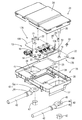
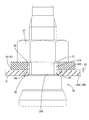
本実施形態の電気接続箱10は、メインバッテリと補助バッテリとを備える自動車等の車両において、メインバッテリ及び補助バッテリからランプ、ワイパー等の電装品へ供給される電力の切り替えに使用されるものである。以下では、説明上、上下方向及び左右方向については、図1の方向を基準として説明するが、電気接続箱10は任意の向きで配置可能である。
The embodiment will be described with reference to FIGS.
The
(電気接続箱10)
電気接続箱10は、図1に示すように、回路部13と、回路部13に重ねられる放熱板23と、回路部13及び放熱板23が収容されるケース30と、2個(複数)のスタッドボルト25と、2個(複数)のナット47とを備えている。
(Electric junction box 10)
As shown in FIG. 1, the
(回路部13)
回路部13は、複数の電子部品12が実装されており、制御基板14と、3枚(複数)のバスバー17A〜17Cとを有する。電子部品12は、図3に示すように、例えばパワーMOSFETからなる複数のスイッチング素子12AとIC(Integrated Circuit )12Bとを含んでいる。複数のスイッチング素子12Aは、バスバー17A〜17Cの通電電流のオンオフを行う。各スイッチング素子12Aは、例えば、裏面側のリード端子がバスバー17A,17Bの上面に半田付けされるとともに、側面側のリード端子が制御基板14の導電路及びバスバー17Cに半田付けされる。
(Circuit part 13)
The
なお、スイッチング素子が3個(複数個)並んでいるのは、スイッチング素子12Aの容量に応じて通電電流を分流させて大電流を通電可能とするためであり、3個のスイッチング素子12Aが反対向きに(電流供給方向とは逆方向)配されているのは、スイッチングオフ時に(寄生ダイオードによる)電流の逆流を防止するためである。
The reason why three (a plurality of) switching elements are arranged is to allow a large current to flow by diverting an energization current according to the capacity of the
制御基板14は、ガラス基材またはガラス不織布基材からなる絶縁板の面に銅箔等からなる導電路がプリント配線技術によって形成されている。制御基板14の周縁部には、コネクタ15が取付けられている。コネクタ15は、コネクタ端子がハウジングに保持されており、コネクタ端子は、ハウジングの後方に延出されて制御基板14の導電路に半田付けされている。コネクタ15には、図示しない相手側コネクタが接続され、スイッチング素子12Aを制御する制御信号や出力信号等が入出力される。
In the
(バスバー17A〜17C)
3枚のバスバー17A〜17Cは、電装品を動作させることが可能な比較的大電流の導電路として用いられ、共に、無酸素銅(C1020,JIS合金記号)からなる金属板材に打ち抜き加工を施して導電路の形状に応じた所定の形状とされている。
(
The three
バスバー17A〜17Cの全体を無酸素銅(C1020)で形成したのは、電気接続箱10のように、大電流を通電するバスバー17A〜17Cについては、発熱を考慮する必要があるためである。導電率は、銅合金(C19020,JIS合金記号)が50%IACS(International Annealed Copper Standard (国際焼きなまし銅線標準))であるのに対して、無酸素銅は、101%IACSと高いため、無酸素銅の方が発熱を低く抑えることができる。
The reason why the
3枚のバスバー17A〜17Cは、図1に示すように、間隔を空けて左右に並んでおり、真ん中のバスバー17Cは、T字状であって、バスバー17A,17B間に配されて前後方向の延びる部分と、左右方向に延びる部分とを有し、全体が制御基板14に重ねられている。左右のバスバー17A,17Bは、長方形状であって、バスバー17Cの隣りに配置されて制御基板14に重なるとともに、制御基板14に重ならない部分が左右(外方)に面一(同一平面)に延出されたバスバー側端子部18A,18Bとされている。
As shown in FIG. 1, the three bus bars 17 </ b> A to 17 </ b> C are arranged side by side with a space therebetween, and the middle bus bar 17 </ b> C has a T shape and is disposed between the bus bars 17 </ b> A and 17 </ b> B in the front-rear direction. , And a portion extending in the left-right direction, and the whole is superimposed on the
(バスバー側端子部18A,18B)
バスバー側端子部18A,18Bは、図2に示すように、長方形状であって、スタッドボルト25の軸部27が挿通される貫通孔19が貫通形成されている。貫通孔19は、軸部27の外周よりもわずかに大きい円形状である。制御基板14、バスバー17A〜17Cには、ネジ24でネジ留めするための円形状のネジ孔22が周縁部寄りの位置等に複数貫通して形成されている。
(Bus
As shown in FIG. 2, the bus bar side terminal portions 18 </ b> A and 18 </ b> B have a rectangular shape, and a through
(放熱板23)
放熱板23は、制御基板14やバスバー17A〜17Cの熱を外部に放散するものであり、例えば、アルミニウムやアルミニウム合金等から形成され、発熱量が大きい6個のスイッチング素子12Aを含む領域のバスバー17A〜17Cに接着剤等により貼り付けられている。
(Heatsink 23)
The
(ケース30)
図1に示すように、ケース30は、合成樹脂製であって、下部ケース31と上部ケース35とを嵌め合わせて形成される。下部ケース31は、制御基板14に間隔を空けて対向する対向壁34を備えるとともに、左右の両側にスタッドボルト25の頭部26を収容する収容室32が下部ケース31の上面に凹み形成されている。
(Case 30)
As shown in FIG. 1, the
収容室32は、下部ケース31の上面にスタッドボルト25の頭部26における矩形状の形状に応じた矩形状に形成されている。収容室32には、内壁の上側に内方に突出する格子状のリブ33が設けられており、このリブ33によりスタッドボルト25の抜け止めがされている。収容室32への頭部26の挿入は、例えば、頭部26の回転角度によってはリブ33を避けて挿入できるようにしたり、頭部26を側方から挿入可能な切欠きを下部ケース31に設けることで頭部26を収容室32に収容すればよい。
The
上部ケース35は、左右の両端側が電線42の端末部を載置可能とされるとともに、電線42の端末部及び電線側端子部43を絶縁するための絶縁壁37を備えている。絶縁壁37の内側には、電線側端子部43及びバスバー側端子部18A,18Bを露出させる開口部38が上下方向に貫通形成されている。開口部38は、電線側端子部43とバスバー側端子部18A,18Bを接続可能な大きさで形成され、電線側端子部43の取付前は、バスバー側端子部18A,18Bが露出する。絶縁壁37は、電線42の端末部及び電線側端子部43を囲むU字状に延びており、電線42が導出される部分には、絶縁壁37は形成されていない。
The
上部ケース35における左右方向の中間部には放熱板23を露出させる放熱孔39が貫通形成されている。放熱孔39は、放熱板23の形状に応じた長方形状であって、放熱孔39の孔縁部は、放熱板23の周縁部を保持して放熱板23を回路部13との間に挟持する保持凸部40とされている。上部ケース35の底面には、図2に示すように、回路部13をネジ24でネジ留めするための複数のネジ孔41が形成されている。
A
電線42は、導体部の周囲が絶縁被覆で覆われた被覆電線であって、端末部で絶縁被覆が剥がされて露出した導体部に電線側端子部43が取付けられている。導体部は例えば多数の金属細線が撚り合わされた撚線とされている。電線側端子部43は、いわゆる丸型の端子であって、板状の接続部44と、バレル部46とを有する。接続部44には、スタッドボルト25の軸部27が挿通される貫通孔45が貫通形成されている。バレル部46は、筒状であって、電線42の導体部が挿通されて圧着される。電線42は、メインバッテリと補助バッテリに接続されている。
The
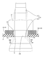
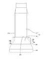
(スタッドボルト25)
スタッドボルト25は、金属製であって、図4,図5に示すように、円柱の外周面27Aにねじ溝が形成された軸部27と、軸部27の下端部に設けられた角柱形の頭部26とを有している。頭部26は、上部が円柱状の円柱部26Bとされ、下部が矩形状の矩形部26Cとされている。ケース30の収容室32に頭部26が収容された際には、矩形部26Cの形状によってスタッドボルト25の回り止めがされる。
(Stud bolt 25)
The
頭部26と軸部27の間の段差部分(円柱部26Bの上面)は、座面26Aとされている。座面26Aの面積(バスバー側端子部18A,18Bに接触する面の面積)は、金属製の六角ナット47からなるナット47が各バスバー側端子部18A,18Bに接触する面の面積よりも小さくなっている。そのため、ボルト締結時には、ナット47に接触する電線側端子部43よりも座面26Aに接触するバスバー側端子部18A,18Bの方が単位面当たりに強い力を受けて変形しやすい。
A step portion between the
スタッドボルト25には、座面26Aと軸部27の外周面27Aとが交差する位置(座面26Aと外周面27Aが交差する円形の線及びその近傍を含む位置)の全周に溝部29が形成されている。溝部29は、下方(軸部27の軸方向に沿う方向)に凹んでおり、内側の端29A(内径)は、外周面27Aと同じ位置(外周面27Aと面一)とされている。溝部29の内側の端29Aと外側の端29Bとの間(即ち、溝部29に重なる位置)に、バスバー側端子部18A,18Bの貫通孔19の孔縁19A(孔壁)が配される。本実施形態では、貫通孔19の孔縁19Aと、溝部29の外側の端29Bとがほぼ同じ位置に配されている。溝部29の深さは、少なくとも座面26Aの高さより低い位置に溝底を有すればよい。
なお、バスバー側端子部18A,18B,電線側端子部43,スタッドボルト25及びナット47により、バスバー17A,17Bと電線42との間を電気的に接続するための接続端子部品が構成されている。
The
The bus bar
スタッドボルト25の形成は、図8に示すように、溝部29が形成されていないスタッドボルトの形状のワークWと、ワークWを加工する上下の金型50A,50Bを用意する。上下の金型50A,50Bの加工面は、スタッドボルトの形状に応じた形状であるが、上型50Aには、溝部29の位置に応じた環状の突部51が下方に突出して形成されている。上下の金型50A,50Bの間にワークWを嵌め込むと(図9)、突部51によって環状の溝部29が形成される。
As shown in FIG. 8, the
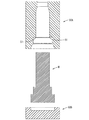
次に、比較例として溝部29を形成しない場合について説明する。図10に示すように、スタッドボルト55の軸部27の外周面27Aと座面26Aとが交差する境界部分には、金型による加工の際に、曲面上に外方に張り出す曲面部60が形成されている。
Next, the case where the
このようなバスバー側端子部18A,18Bに電線側端子部43を重ねて各貫通孔19,45にスタッドボルト25の軸部27を挿通してバスバー側端子部18A,18Bを座面26Aに接触させる方向に移動する。ここで、バスバー側端子部18A,18Bの貫通孔19は、端子部間の接触面積を確保するために、貫通孔19の孔径が外周面27Aよりわずかに大きい程度の大きさとされているため、曲面部60にバスバー側端子部18A,18Bの貫通孔19の孔縁19Aが引っ掛かる。そのまま、ナット47を締め付けていくと、貫通孔19の孔縁19Aが曲面部60に沿って変形し、バスバー側端子部18A,18Bと電線側端子部43との間に隙間G1を生じさせ、バスバー側端子部18A,18Bと電線側端子部43との間の接触面積が少なくなり、バスバー側端子部18A,18Bと電線側端子部43との間の接触抵抗が増加する。
The electric wire
また、仮に、図11に示すように、バスバー側端子部58について、貫通孔19よりも孔径が大きい貫通孔57を形成すると、貫通孔57の孔縁が曲面部60に引っ掛かりにくくはなるものの、バスバー側端子部58と電線側端子部43との間の接触面積が少なくなるとともに、図12に示すように、貫通孔57の中心と軸部27の軸の位置とがずれて、バスバー側端子部58が左右の一方に偏って配置されうる。この場合、バスバー側端子部58と座面26Aとの間に隙間G2が生じ、スタッドボルト25とナット47の締結の際の力がバスバー側端子部58と電線側端子部43との間に均一に与えられないおそれがある。
In addition, as shown in FIG. 11, if the through
これに対して、本実施形態では、座面26Aと軸部27の外周面27Aとが交差する位置の全周に溝部29が形成されているため、バスバー側端子部18A,18Bの貫通孔19の孔径を小さくしても、バスバー側端子部18A,18Bの貫通孔19を軸部27に挿通した際に、貫通孔19の孔縁19Aが曲面部60に引っ掛かることがない。したがって、バスバー側端子部18A,18Bと電線側端子部43との接触面積の減少を抑制できるため、端子部間の接触抵抗の増加を抑制することが可能になる。
On the other hand, in this embodiment, since the
上記したように、溝部29は、曲面部60を設けないために形成されるのであるから、溝部29の幅寸法(内側の端29Aと外側の端29Bの間の寸法)は、溝部29がない場合のスタッドボルトの加工時に形成される曲面部60の幅寸法以上とされる。
As described above, since the
次に、電気接続箱10の製造方法について説明する。
無酸素銅からなる金属板材に打ち抜き加工を施して、複数のバスバー17A〜17Cを形成する。次に、バスバー17A〜17Cを互いに所定の隙間を空けて配置し、銅箔の導電路が印刷された制御基板14を、バスバー17A〜17C上の所定の位置に、例えば熱硬化性の接着シートを用いて、熱プレス機を用いて貼り付ける。
Next, a method for manufacturing the
A plurality of
次に、制御基板14及びバスバー17A〜17Cに電子部品12を実装する。スイッチング素子12AとしてのMOSFETについては、3個ずつ並列に、ソース端子同士が対向するように配置し、バスバー17A,17Bには、ドレイン端子を半田付けして接続する。また、バスバー17Cに、ソース端子を半田付けして接続すると、対向配置されたMOSFETのソース端子同士が電気的に接続される。全ての電子部品12が実装されると回路構成体が形成される。
Next, the
次に、ワークWを金型50A,50Bで挟んで溝部29を形成したスタッドボルト25を下部ケース31の所定の位置に装着する。そして、バスバー側端子部18A,18Bの貫通孔19にスタッドボルト25の軸部27を挿通しつつ下部ケース31の上に回路構成体を載置してネジ24でネジ留めする。
Next, the
次に、上部ケース35を被せてネジ留めして下部ケース31に固定する。次に、スタッドボルト25の軸部27に電線42の端末部に取付けられた電線側端子部43の貫通孔45を挿通してバスバー側端子部18A,18Bと電線側端子部43とを重ねる。そして、ナット47をスタッドボルト25に螺合させて締結する。
Next, the
本実施形態によれば、以下の作用、効果を奏する。
本実施形態によれば、スタッドボルト25(ボルト)には、座面26Aと軸部27の外周面27Aとが交差する位置の全周に溝部29が形成されているため、座面26Aと軸部27の外周面27Aとが交差する位置に曲面が張り出すことがない。これにより、バスバー側端子部18A,18Bについて、貫通孔19の孔径を小さくしても、貫通孔19の孔縁19Aが座面26Aと軸部27の外周面27Aとが交差する位置に引っ掛かることがない。よって、バスバー側端子部18A,18Bと電線側端子部43とを座面26Aの上に隙間なく重ねて所定の位置に配置することが可能になるため、バスバー側端子部18A,18Bと電線側端子部43との間の接触抵抗の増加を抑制することが可能になる。
According to this embodiment, the following operations and effects are achieved.
According to the present embodiment, the stud bolt 25 (bolt) has the
また、溝部29は、下向(軸部27の軸方向に沿う方向)に凹んでいる。
このようにすれば、例えば溝部29が座面26Aに沿う方向に凹んでいる構成と比較して金型による溝部29の形成が容易になる。
The
In this way, for example, the
また、バスバー側端子部18A,18Bの貫通孔19の孔縁19Aは、溝部29の内側の端29Aと外側の端29Bの間(溝部29に重なる位置)に配されている。
このようにすれば、貫通孔19の孔縁19Aを溝部29の外側に配する場合と比較して、貫通孔19の孔径が小さくなるため、バスバー側端子部18A,18Bと電線側端子部43との間の接触面積を大きくすることができる。
Further, the
In this way, the hole diameter of the through
大電流を通電するバスバー17A〜17Cを無酸素銅で形成したのは、発熱を低く抑えることができるためであるが、その反面、無酸素銅は、銅合金等と比較して変形しやすい。したがって、仮に座面26Aと軸部27の外周面27Aとが交差する位置に曲面部60が形成されていると、貫通孔19の孔縁19Aが曲面部60に引っ掛かると容易に変形する。本実施形態では、曲面部60に代えて溝部29が形成されているため、バスバー側端子部18A,18Bが無酸素銅で形成されているために変形しやすい構成において、バスバー側端子部18A,18Bの変形を抑制することができる。
The reason why the bus bars 17A to 17C through which a large current is passed is made of oxygen-free copper is that heat generation can be suppressed to a low level, but on the other hand, oxygen-free copper is more easily deformed than copper alloys and the like. Therefore, if the
<他の実施形態>
本発明は上記記述及び図面によって説明した実施形態に限定されるものではなく、例えば次のような実施形態も本発明の技術的範囲に含まれる。
(1)上記実施形態では、溝部29の外側の端29Bは、貫通孔19の孔縁19Aとほぼ同じ位置に形成されていたが、これに限られず、貫通孔19の孔縁19Aを外側の端29Bよりも内側としても外側としてもよい。
<Other embodiments>
The present invention is not limited to the embodiments described with reference to the above description and drawings. For example, the following embodiments are also included in the technical scope of the present invention.
(1) In the above embodiment, the
(2)溝部29は、軸部27の軸方向に沿う方向に凹んでいる構成としたが、これに限られない。例えば、座面26Aに沿う方向に凹んでいる溝部を設けてもよい。
(2) Although the
(3)上記実施形態では、バスバー側端子部18A,18Bの上に電線側端子部43が重ねられていたが、バスバー側端子部18A,18Bの下に電線側端子部43が重ねられていてもよい。例えば、バスバー側端子部18A,18Bの下に電線側端子部43が、例えばバスバー側端子部18A,18Bの板面に沿う方向からスライド等して重ねられるようにしてもよい。
(3) In the above embodiment, the electric wire
(4)上記実施形態では、バスバー17A〜17Cは、純銅における無酸素銅で形成されていたが、これに限られない。例えば、無酸素銅以外の純銅(純度99.9%以上)や、純銅よりも銅の純度が低い銅合金等の材料でバスバー17A〜17Cを形成してもよい。 (4) In the above embodiment, the bus bars 17A to 17C are made of oxygen-free copper in pure copper, but are not limited thereto. For example, the bus bars 17A to 17C may be formed of a material such as pure copper (purity of 99.9% or more) other than oxygen-free copper, or a copper alloy whose purity is lower than that of pure copper.
(5)バスバー側端子部18A,18Bや電線側端子部43の形状は、上記実施形態の形状に限られず、少なくともバスバー側端子部と電線側端子部43を重ねることができれば、種々の形状に変更してもよい。
(5) the shape of the bus bar-
(6)上記実施形態では、メインバッテリ及び補助バッテリから電装品へ供給される電力の切り替えに使用される電気接続箱10としたが、これに限られない。例えば、車両の電源から負荷に至る経路に配される他の用途の電気接続箱であってもよい。また、電気接続箱以外の端子部間の接続構造に本発明を適用してもよい。例えば、メインバッテリや補助バッテリ等のバッテリの端子をバスバー側端子としてもよい。
(6) In the above embodiment, the
10: 電気接続箱
12: 電子部品
13: 回路部
17A〜17C: バスバー
18A,18B: バスバー側端子部
19,45: 貫通孔
23: 放熱板
25: スタッドボルト(ボルト)
26: 頭部
26A: 座面
27: 軸部
27A: 外周面
29: 溝部
30: ケース
42: 電線
43: 電線側端子部
44: 接続部
47: ナット
10: Electrical connection box 12: Electronic component 13:
26:
Claims (4)
前記回路部が収容されるケースと、
前記バスバーに設けられ、貫通孔が形成されたバスバー側端子部と、
電線に接続され、貫通孔が形成された電線側端子部と、
軸部と頭部とを有するボルトと、
前記ボルトに締結されるナットと、を備え、
前記バスバー側端子部の貫通孔及び前記電線側端子部の貫通孔のそれぞれに前記ボルトの軸部が挿通されて前記バスバー側端子部及び前記電線側端子部が前記ボルトの座面上に重ねられるとともに、前記ボルトは、前記座面と前記軸部の外周面とが交差する位置の全周に溝部が形成されており、
前記溝部は、前記軸部の軸方向に沿う方向に凹んでいる、電気接続箱。 A circuit unit having a bus bar as a conductive path, on which electronic components are mounted;
A case in which the circuit unit is accommodated;
A bus bar side terminal portion provided in the bus bar and having a through-hole formed therein;
An electric wire side terminal portion connected to the electric wire and having a through hole; and
A bolt having a shaft and a head;
A nut fastened to the bolt,
The shaft portion of the bolt is inserted into each of the through hole of the bus bar side terminal portion and the through hole of the wire side terminal portion, and the bus bar side terminal portion and the wire side terminal portion are overlapped on the seat surface of the bolt. And the groove part is formed in the perimeter of the position where the above-mentioned bolt and the peripheral surface of the above-mentioned shaft part intersect with the above-mentioned bolt ,
The groove portion is an electrical junction box that is recessed in a direction along the axial direction of the shaft portion .
前記回路部が収容されるケースと、
前記バスバーに設けられ、貫通孔が形成されたバスバー側端子部と、
電線に接続され、貫通孔が形成された電線側端子部と、
軸部と頭部とを有するボルトと、
前記ボルトに締結されるナットと、を備え、
前記バスバー側端子部の貫通孔及び前記電線側端子部の貫通孔のそれぞれに前記ボルトの軸部が挿通されて前記バスバー側端子部及び前記電線側端子部が前記ボルトの座面上に重ねられるとともに、前記ボルトは、前記座面と前記軸部の外周面とが交差する位置の全周に溝部が形成されており、
前記バスバー側端子部及び前記電線側端子部のうち、前記座面に接する側の貫通孔の孔縁は、前記溝部に重なる位置に配されている、電気接続箱。 A circuit unit having a bus bar as a conductive path, on which electronic components are mounted;
A case in which the circuit unit is accommodated;
A bus bar side terminal portion provided in the bus bar and having a through-hole formed therein;
An electric wire side terminal portion connected to the electric wire and having a through hole; and
A bolt having a shaft and a head;
A nut fastened to the bolt,
The shaft portion of the bolt is inserted into each of the through hole of the bus bar side terminal portion and the through hole of the wire side terminal portion, and the bus bar side terminal portion and the wire side terminal portion are overlapped on the seat surface of the bolt. And the groove part is formed in the perimeter of the position where the above-mentioned bolt and the peripheral surface of the above-mentioned shaft part intersect with the above-mentioned bolt,
Of the bus bar side terminal part and the electric wire side terminal part, the hole edge of the through hole on the side in contact with the seating surface is arranged in a position overlapping the groove part .
電線に接続され、貫通孔が形成された電線側端子部と、
軸部と頭部とを有するボルトと、
前記ボルトに締結されるナットと、を備え、
前前記バスバー側端子部の貫通孔及び前記電線側端子部の貫通孔のそれぞれに前記ボルトの軸部が挿通されて前記バスバー側端子部及び前記電線側端子部が前記ボルトの座面上に重ねられるとともに、前記ボルトは、前記座面と前記軸部の外周面とが交差する位置の全周に溝部が形成されており、
前記溝部は、前記軸部の軸方向に沿う方向に凹んでいる、接続端子部品。 A bus bar side terminal portion provided in a bus bar as a conductive path, in which a through hole is formed;
An electric wire side terminal portion connected to the electric wire and having a through hole; and
A bolt having a shaft and a head;
A nut fastened to the bolt,
The shaft portion of the bolt is inserted into each of the through hole of the front bus bar side terminal portion and the through hole of the wire side terminal portion, and the bus bar side terminal portion and the wire side terminal portion are overlapped on the seat surface of the bolt. In addition, the bolt has a groove formed on the entire periphery of the position where the seat surface and the outer peripheral surface of the shaft portion intersect.
The groove portion is a connection terminal component that is recessed in a direction along the axial direction of the shaft portion .
電線に接続され、貫通孔が形成された電線側端子部と、
軸部と頭部とを有するボルトと、
前記ボルトに締結されるナットと、を備え、
前前記バスバー側端子部の貫通孔及び前記電線側端子部の貫通孔のそれぞれに前記ボルトの軸部が挿通されて前記バスバー側端子部及び前記電線側端子部が前記ボルトの座面上に重ねられるとともに、前記ボルトは、前記座面と前記軸部の外周面とが交差する位置の全周に溝部が形成されており、
前記バスバー側端子部及び前記電線側端子部のうち、前記座面に接する側の貫通孔の孔縁は、前記溝部に重なる位置に配されている、接続端子部品。 A bus bar side terminal portion provided in a bus bar as a conductive path, in which a through hole is formed;
An electric wire side terminal portion connected to the electric wire and having a through hole; and
A bolt having a shaft and a head;
A nut fastened to the bolt,
The shaft portion of the bolt is inserted into each of the through hole of the front bus bar side terminal portion and the through hole of the wire side terminal portion, and the bus bar side terminal portion and the wire side terminal portion are overlapped on the seat surface of the bolt. In addition, the bolt has a groove formed on the entire periphery of the position where the seat surface and the outer peripheral surface of the shaft portion intersect .
Of the bus bar side terminal portion and the electric wire side terminal portion, a connection terminal component in which a hole edge of a through hole on a side in contact with the seating surface is arranged at a position overlapping the groove portion .
Priority Applications (4)
| Application Number | Priority Date | Filing Date | Title |
|---|---|---|---|
| JP2015033983A JP6287891B2 (en) | 2015-02-24 | 2015-02-24 | Electrical connection box and connection terminal parts |
| US15/549,511 US10141660B2 (en) | 2015-02-24 | 2016-02-03 | Electrical connection box and connection terminal component |
| CN201680010559.XA CN107251348B (en) | 2015-02-24 | 2016-02-03 | Electric connection box and connection terminal component |
| PCT/JP2016/053175 WO2016136408A1 (en) | 2015-02-24 | 2016-02-03 | Electrical connection box and connection terminal component |
Applications Claiming Priority (1)
| Application Number | Priority Date | Filing Date | Title |
|---|---|---|---|
| JP2015033983A JP6287891B2 (en) | 2015-02-24 | 2015-02-24 | Electrical connection box and connection terminal parts |
Publications (3)
| Publication Number | Publication Date |
|---|---|
| JP2016158373A JP2016158373A (en) | 2016-09-01 |
| JP2016158373A5 JP2016158373A5 (en) | 2017-08-17 |
| JP6287891B2 true JP6287891B2 (en) | 2018-03-07 |
Family
ID=56788388
Family Applications (1)
| Application Number | Title | Priority Date | Filing Date |
|---|---|---|---|
| JP2015033983A Active JP6287891B2 (en) | 2015-02-24 | 2015-02-24 | Electrical connection box and connection terminal parts |
Country Status (4)
| Country | Link |
|---|---|
| US (1) | US10141660B2 (en) |
| JP (1) | JP6287891B2 (en) |
| CN (1) | CN107251348B (en) |
| WO (1) | WO2016136408A1 (en) |
Families Citing this family (10)
| Publication number | Priority date | Publication date | Assignee | Title |
|---|---|---|---|---|
| JP6252872B2 (en) * | 2015-02-24 | 2017-12-27 | 株式会社オートネットワーク技術研究所 | Electrical connection box and connection terminal parts |
| JP6499124B2 (en) * | 2016-06-30 | 2019-04-10 | 矢崎総業株式会社 | Conductive member and electrical junction box |
| JP6620725B2 (en) | 2016-11-14 | 2019-12-18 | 株式会社オートネットワーク技術研究所 | Electrical junction box |
| JP6696442B2 (en) | 2017-01-12 | 2020-05-20 | 三菱電機株式会社 | Semiconductor module |
| CN109874386B (en) * | 2017-04-27 | 2021-09-10 | 富士电机株式会社 | Electronic component and power conversion device |
| JP6919599B2 (en) * | 2018-03-05 | 2021-08-18 | 住友電装株式会社 | Electrical junction box |
| KR102554431B1 (en) | 2018-09-05 | 2023-07-13 | 삼성전자주식회사 | Semiconductor device and manufacturing method of the same |
| JP7192651B2 (en) * | 2019-05-10 | 2022-12-20 | 株式会社オートネットワーク技術研究所 | electric junction box |
| CN114914857A (en) * | 2021-02-08 | 2022-08-16 | 住友电装株式会社 | Wire harness and protector |
| CN115832996B (en) * | 2022-12-22 | 2024-06-07 | 深圳市欧亚特电器设备有限公司 | Fireproof bus duct capable of preventing electromagnetic interference |
Family Cites Families (24)
| Publication number | Priority date | Publication date | Assignee | Title |
|---|---|---|---|---|
| DE19535537A1 (en) * | 1995-09-25 | 1997-03-27 | Profil Verbindungstechnik Gmbh | Bolt element, method for inserting the same, assembly part and rivet die |
| JP3409239B2 (en) * | 1997-06-30 | 2003-05-26 | 住友電装株式会社 | Connection structure between battery and electrical junction box |
| US6322376B1 (en) * | 2000-03-31 | 2001-11-27 | Yazaki North America | Stud bolt holder for a power distribution box |
| JP2004072907A (en) * | 2002-08-06 | 2004-03-04 | Sumitomo Wiring Syst Ltd | Electric junction box |
| DE202004000463U1 (en) * | 2004-01-13 | 2004-08-19 | Textron Verbindungstechnik Gmbh & Co. Ohg | Bolts that can be pressed into a sheet to prevent twisting and squeezing |
| JP2006331923A (en) * | 2005-05-27 | 2006-12-07 | Sumitomo Wiring Syst Ltd | Electric connection box |
| JP2007028773A (en) * | 2005-07-14 | 2007-02-01 | Sumitomo Wiring Syst Ltd | Vehicle mounted electric connection box |
| JP5074744B2 (en) * | 2006-11-15 | 2012-11-14 | 矢崎総業株式会社 | Electrical junction box |
| JP5030226B2 (en) * | 2007-10-17 | 2012-09-19 | 矢崎総業株式会社 | Electrical junction box |
| JP4911009B2 (en) | 2007-12-11 | 2012-04-04 | 株式会社デンソー | Semiconductor device including bus bar and bus bar |
| JP5131981B2 (en) * | 2008-07-16 | 2013-01-30 | 矢崎総業株式会社 | Electrical junction box terminal mounting structure |
| JP5157765B2 (en) * | 2008-09-03 | 2013-03-06 | 住友電装株式会社 | Electrical junction box |
| JP5360582B2 (en) * | 2009-10-28 | 2013-12-04 | 住友電装株式会社 | Electrical junction box |
| JP5294084B2 (en) * | 2009-10-28 | 2013-09-18 | 住友電装株式会社 | Stud bolt assembly and electrical junction box with stud bolt assembly |
| ES2687682T3 (en) * | 2009-12-22 | 2018-10-26 | R B & W Manufacturing Llc | Nut with thickening of lug |
| JP5606200B2 (en) * | 2010-07-23 | 2014-10-15 | 矢崎総業株式会社 | Fuse block device |
| CN102029956B (en) * | 2010-12-06 | 2013-01-23 | 力帆实业(集团)股份有限公司 | Installation assembly of automotive electric control box |
| JP5800624B2 (en) * | 2011-07-28 | 2015-10-28 | 矢崎総業株式会社 | Busbar end structure of electrical junction box |
| DE102012001086A1 (en) * | 2012-01-20 | 2013-07-25 | Profil Verbindungstechnik Gmbh & Co. Kg | Bolt element and method for attaching a bolt element to a component made of a composite material |
| JP5809569B2 (en) * | 2012-01-23 | 2015-11-11 | 矢崎総業株式会社 | Electrical junction box |
| JP6018892B2 (en) * | 2012-11-30 | 2016-11-02 | 矢崎総業株式会社 | Electrical junction box |
| JP6106518B2 (en) * | 2013-05-09 | 2017-04-05 | 矢崎総業株式会社 | Round terminal fixing structure |
| US9217456B2 (en) * | 2013-06-11 | 2015-12-22 | Chicony Power Technology Co., Ltd. | Waterproof, dustproof, breathing bolt |
| CN103647241A (en) * | 2013-11-22 | 2014-03-19 | 西安正麒电气有限公司 | Junction box for electric vehicle motor controller |
-
2015
- 2015-02-24 JP JP2015033983A patent/JP6287891B2/en active Active
-
2016
- 2016-02-03 US US15/549,511 patent/US10141660B2/en active Active
- 2016-02-03 CN CN201680010559.XA patent/CN107251348B/en active Active
- 2016-02-03 WO PCT/JP2016/053175 patent/WO2016136408A1/en active Application Filing
Also Published As
| Publication number | Publication date |
|---|---|
| JP2016158373A (en) | 2016-09-01 |
| US10141660B2 (en) | 2018-11-27 |
| WO2016136408A1 (en) | 2016-09-01 |
| US20180034169A1 (en) | 2018-02-01 |
| CN107251348B (en) | 2019-05-03 |
| CN107251348A (en) | 2017-10-13 |
Similar Documents
| Publication | Publication Date | Title |
|---|---|---|
| JP6287891B2 (en) | Electrical connection box and connection terminal parts | |
| JP6252872B2 (en) | Electrical connection box and connection terminal parts | |
| JP6213776B2 (en) | Switching board | |
| US10842015B2 (en) | Conductive member, circuit assembly, and method for manufacturing conductive member | |
| JP2006060924A (en) | Electrical connection box | |
| WO2020105391A1 (en) | Circuit structure | |
| US20160286667A1 (en) | Fixing element for connecting printed circuit board and busbar, and power distributor having the same | |
| US20210247243A1 (en) | Circuit board assembly | |
| CN112352473B (en) | Circuit substrate | |
| WO2017073258A1 (en) | Power storage unit | |
| US10763048B2 (en) | Electrical junction box | |
| WO2020105393A1 (en) | Circuit structure | |
| CN112889352A (en) | Circuit structure and electric connection box | |
| EP2200408B1 (en) | Circuit board device, in particular for an electric power consuming device in a motor vehicle | |
| JP2020022235A (en) | Power conversion device and bus bar | |
| WO2024185072A1 (en) | Circuit body | |
| JP7192918B1 (en) | Busbar heat dissipation structure and inverter device | |
| JP2010135239A (en) | Power feeding material and lamp tool for vehicle | |
| JP4038099B2 (en) | Electronic component mounting structure of large current control unit | |
| KR200458485Y1 (en) | Power supply connector for junction box of vehicle | |
| JP2011029436A (en) | Metal core substrate with caulking terminal | |
| JP2015053394A (en) | Printed board | |
| JP2006310703A (en) | Electronic component module |
Legal Events
| Date | Code | Title | Description |
|---|---|---|---|
| A621 | Written request for application examination |
Free format text: JAPANESE INTERMEDIATE CODE: A621 Effective date: 20170531 |
|
| A521 | Written amendment |
Free format text: JAPANESE INTERMEDIATE CODE: A523 Effective date: 20170707 |
|
| A131 | Notification of reasons for refusal |
Free format text: JAPANESE INTERMEDIATE CODE: A131 Effective date: 20171102 |
|
| A521 | Written amendment |
Free format text: JAPANESE INTERMEDIATE CODE: A523 Effective date: 20171219 |
|
| TRDD | Decision of grant or rejection written | ||
| A01 | Written decision to grant a patent or to grant a registration (utility model) |
Free format text: JAPANESE INTERMEDIATE CODE: A01 Effective date: 20180109 |
|
| A61 | First payment of annual fees (during grant procedure) |
Free format text: JAPANESE INTERMEDIATE CODE: A61 Effective date: 20180122 |
|
| R150 | Certificate of patent or registration of utility model |
Ref document number: 6287891 Country of ref document: JP Free format text: JAPANESE INTERMEDIATE CODE: R150 |