JP6281193B2 - Laser scanning microscope system - Google Patents
Laser scanning microscope system Download PDFInfo
- Publication number
- JP6281193B2 JP6281193B2 JP2013113572A JP2013113572A JP6281193B2 JP 6281193 B2 JP6281193 B2 JP 6281193B2 JP 2013113572 A JP2013113572 A JP 2013113572A JP 2013113572 A JP2013113572 A JP 2013113572A JP 6281193 B2 JP6281193 B2 JP 6281193B2
- Authority
- JP
- Japan
- Prior art keywords
- laser
- light emission
- sampling
- signal
- intermittent
- Prior art date
- Legal status (The legal status is an assumption and is not a legal conclusion. Google has not performed a legal analysis and makes no representation as to the accuracy of the status listed.)
- Expired - Fee Related
Links
Images


Classifications
-
- G—PHYSICS
- G01—MEASURING; TESTING
- G01N—INVESTIGATING OR ANALYSING MATERIALS BY DETERMINING THEIR CHEMICAL OR PHYSICAL PROPERTIES
- G01N21/00—Investigating or analysing materials by the use of optical means, i.e. using sub-millimetre waves, infrared, visible or ultraviolet light
- G01N21/62—Systems in which the material investigated is excited whereby it emits light or causes a change in wavelength of the incident light
- G01N21/63—Systems in which the material investigated is excited whereby it emits light or causes a change in wavelength of the incident light optically excited
- G01N21/64—Fluorescence; Phosphorescence
- G01N21/645—Specially adapted constructive features of fluorimeters
- G01N21/6456—Spatial resolved fluorescence measurements; Imaging
- G01N21/6458—Fluorescence microscopy
Description
本開示は、レーザー走査型顕微鏡システムに関する。 The present disclosure relates to a laser scanning microscope system.
従来、例えば下記の特許文献1には、被検物を走査する走査機器を含む走査型顕微鏡であって、発振パルス周波数とサンプリング周波数との間の同調化を行う走査型顕微鏡が記載されている。 Conventionally, for example, the following Patent Document 1 describes a scanning microscope including a scanning device that scans a test object and that performs synchronization between an oscillation pulse frequency and a sampling frequency. .
近年では、半導体レーザーを用いたMOPA型の光源により100W以上の高出力を有するものが開発されている。しかしながら、生体を測定対象とする場合、レーザー光のパワーが強いと、生体に対するダメージが大きくなる問題がある。 In recent years, a MOPA type light source using a semiconductor laser having a high output of 100 W or more has been developed. However, when a living body is a measurement target, there is a problem that damage to the living body increases when the power of the laser beam is strong.
生体に対するダメージを抑えるためには、レーザー光の平均パワーを低くしてピークパワーを高くすることが有効である。このため、レーザー光を間欠的に発光させて、生体に対するダメージを抑えることが考えられる。 In order to suppress damage to the living body, it is effective to increase the peak power by lowering the average power of the laser beam. For this reason, it is possible to suppress damage to the living body by intermittently emitting laser light.
しかしながら、レーザー走査型顕微鏡においては、対象物において励起した蛍光体をPMT等の検出器で電気信号に変換するが、レーザー光を間欠的に発光させた場合、変換後のA/D変換のサンプリングによっては、取得した画像が劣化する問題がある。 However, in a laser scanning microscope, a phosphor excited in an object is converted into an electric signal by a detector such as a PMT. However, when laser light is emitted intermittently, sampling of A / D conversion after conversion is performed. Depending on the case, there is a problem that the acquired image deteriorates.
上記特許文献1には、発振パルス周波数とサンプリング周波数との間の同調化を行うことが記載されているが、間欠発光を行った場合の間欠発光周期については何ら考慮されていない。また、特許文献1に記載された技術では、パルス発光に同期した高速サンプリングをしたとしても、分解能が向上することはあり得ず、信号量も増加することは困難である。 Patent Document 1 describes that tuning is performed between the oscillation pulse frequency and the sampling frequency, but no consideration is given to the intermittent light emission period when intermittent light emission is performed. In the technique described in Patent Document 1, even if high-speed sampling synchronized with pulsed light emission is performed, the resolution cannot be improved, and it is difficult to increase the signal amount.
そこで、レーザー光を間欠的に発光させた場合に、対象物において励起した蛍光体による電気信号を最適にサンプリングして画像の劣化を抑えることが望まれていた。 Therefore, when laser light is intermittently emitted, it has been desired to optimally sample an electrical signal from a phosphor excited in an object to suppress image deterioration.
本開示によれば、所定の周波数のレーザー光を出射するモードロックレーザー部と、前記モードロックレーザー部から出射されるレーザー光を所定の間欠発光周期で間欠発光させる間欠発光部と、間欠発光された前記レーザー光を受けて対象物から励起した蛍光体を電気信号に変換する検出器と、前記電気信号を前記間欠発光周期と同期したサンプリング周期でサンプリングするA/D変換部と、を備える、レーザー走査型顕微鏡システムが提供される。 According to the present disclosure, a mode-locked laser unit that emits laser light having a predetermined frequency, an intermittent light-emitting unit that intermittently emits laser light emitted from the mode-locked laser unit at a predetermined intermittent light emission period, and intermittent light emission. A detector that converts the phosphor excited from the object by receiving the laser light into an electrical signal, and an A / D converter that samples the electrical signal at a sampling period synchronized with the intermittent light emission period, A laser scanning microscope system is provided.
前記サンプリング及び前記間欠発光に係る周波数及び位相が一致するものであっても良い。 The frequency and phase related to the sampling and the intermittent light emission may coincide with each other.
また、前記モードロックレーザー部は、二光子励起のためのレーザー光を出射するものであっても良い。 The mode-locked laser unit may emit laser light for two-photon excitation.
また、前記A/D変換部に対して前記サンプリング周期を与えるサンプリング信号と、前記間欠発光部に対して前記間欠発光周期を与える間欠発光信号とが同一の信号であっても良い。 The sampling signal that gives the sampling period to the A / D converter and the intermittent light emission signal that gives the intermittent light emission period to the intermittent light emitting part may be the same signal.
また、前記A/D変換部に対して前記サンプリング周期を与えるサンプリング信号を発生させるサンプリング信号発生部と、前記間欠発光部に対して前記間欠発光周期を与える間欠発光信号を発生させる間欠発光信号発生部と、を更に備え、前記サンプリング信号と前記間欠発光信号とを同一のクロックに基づいて発生させるものであっても良い。 In addition, a sampling signal generation unit that generates a sampling signal that gives the sampling cycle to the A / D conversion unit, and an intermittent light emission signal generation that generates an intermittent light emission signal that gives the intermittent light emission cycle to the intermittent light emission unit. The sampling signal and the intermittent light emission signal may be generated based on the same clock.
また、前記モードロックレーザー部又は前記間欠発光部は、前記レーザー光を所定の有効発光期間のみ前記対象物に入射させるものであっても良い。 Further, the mode-locked laser unit or the intermittent light emitting unit may cause the laser light to be incident on the object only during a predetermined effective light emitting period.
また、前記レーザー光を前記対象物の表面の第1の方向へ走査する第1のガルバノミラーと、前記レーザー光を前記対象物の表面の前記第1の方向と直交する第2の方向へ走査する第2のガルバノミラーと、前記第1及び第2のガルバノミラーを制御するガルバノミラー制御部と、を備え、前記ガルバノミラー制御部は、前記第1の方向への走査が完了すると、前記第1の方向の始点位置に前記レーザー光を戻すとともに、前記レーザー光の1ライン分だけ前記第2の方向への走査を行い、その後、再び前記第1の方向への走査を行い、前記有効発光期間は、前記第1の方向へ走査を行う期間の少なくとも一部であっても良い。 A first galvanometer mirror that scans the laser beam in a first direction on the surface of the object; and a scan that scans the laser beam in a second direction that is orthogonal to the first direction on the surface of the object. And a galvano mirror control unit that controls the first and second galvano mirrors, and the galvano mirror control unit completes scanning in the first direction when the scanning in the first direction is completed. The laser beam is returned to the start position in the direction 1, and the scanning in the second direction is performed by one line of the laser beam, and then the scanning in the first direction is performed again, and the effective light emission is performed. The period may be at least a part of the period during which scanning is performed in the first direction.
また、前記検出器から出力された前記電気信号を帯域制限して前記A/D変換部へ入力するローパスフィルタを備え、前記ローパスフィルタは、前記サンプリングの周波数に対してナイキストのサンプリング定理が成立するように前記帯域制限を行うものであっても良い。 In addition, the low-pass filter that band-limits the electric signal output from the detector and inputs the electric signal to the A / D converter, and the low-pass filter satisfies the Nyquist sampling theorem with respect to the sampling frequency. As described above, the band limitation may be performed.
また、前記ローパスフィルタは、前記サンプリングの周波数の1/2以下となるように前記帯域制限を行うものであっても良い。 The low-pass filter may perform the band limitation so that the frequency becomes 1/2 or less of the sampling frequency.
本開示によれば、レーザー光を間欠的に発光させた場合に、対象物において励起した蛍光体による電気信号を最適にサンプリングして画像の劣化を抑えることが可能となる。 According to the present disclosure, when laser light is intermittently emitted, it is possible to optimally sample an electrical signal from a phosphor excited in an object and suppress deterioration of an image.
以下に添付図面を参照しながら、本開示の好適な実施の形態について詳細に説明する。なお、本明細書及び図面において、実質的に同一の機能構成を有する構成要素については、同一の符号を付することにより重複説明を省略する。 Hereinafter, preferred embodiments of the present disclosure will be described in detail with reference to the accompanying drawings. In addition, in this specification and drawing, about the component which has the substantially same function structure, duplication description is abbreviate | omitted by attaching | subjecting the same code | symbol.
なお、説明は以下の順序で行うものとする。
1・顕微鏡システムについて
2.光源の構成例
3.顕微鏡システムの構成例
4.サンプリング周期と間欠発光周期の関係
5.サンプリング周期と間欠駆動周期を一致させるための構成例
6.ローパスフィルタの構成
7.レーザー光の光パルスとレーザー光の変調との同期
8.光学的分解能とサンプリング周波数の関係
The description will be made in the following order.
1. About the
[1・顕微鏡システムについて]
まず、図1を参照しながら、本開示の一実施形態に係る顕微鏡システムについて説明する。図1は、本実施形態に係る顕微鏡システムの一例を示す模式図である。この顕微鏡システムは、生体解析用のレーザー走査型顕微鏡であり、特に二光子励起の光源を有する顕微鏡システムである。図1に示すように、顕微鏡システム1000は、顕微鏡本体100と、光源200と、制御部300とを有して構成されている。
[1. About the microscope system]
First, a microscope system according to an embodiment of the present disclosure will be described with reference to FIG. FIG. 1 is a schematic diagram illustrating an example of a microscope system according to the present embodiment. This microscope system is a laser scanning microscope for biological analysis, and in particular, a microscope system having a two-photon excitation light source. As shown in FIG. 1, the microscope system 1000 includes a microscope
顕微鏡本体100は、レーザー走査型顕微鏡として構成され、測定サンプルSを、当該測定サンプルの縦方向、横方向奥行き方向の3次元に走査して、測定サンプルSの拡大画像群に対応する画像データ群を生成する。このため、顕微鏡本体100は、光電子増倍管(PMT)とガルバノミラーを有して構成されている。顕微鏡本体100の構成については、後で詳細に説明する。
The microscope
光源200は、パルスレーザーを用いるものであり、外部共振器を備えたレーザー(Mode Locked Laser Diode(以下、MLLDと称する))と半導体光増幅アンプ(SOA)を有して構成されるMOPA(Master Oscillator Power Amplifier)型の光源である。近年では、半導体レーザーを用いたMOPA型の光源により100W以上の高出力を有するものが開発されている。この光源は、低価格且つ小型であるという特徴から、ミドルレンジの多光子顕微鏡への搭載が可能となれば、幅広い研究機関に用いられる可能性が広がり、医療や製薬の分野で大きな貢献が期待できる。本実施形態では、このようなMOPA型の光源を用いた顕微鏡システム、特に二光子励起の光源を用いたシステムについて説明する。
The
制御部300は、顕微鏡本体100、および光源200を制御する機能を有する。制御部300の構成については後で詳細に説明する。
The
[2.光源の構成例]
図2は、光源200の構成を詳細に示す模式図である。光源200は、モードロック発振型レーザーと光アンプを組み合わせたMOPA210と、波長変換モジュール(OPO)250とから構成されている。MOPA210は、モードロックレーザー部(Mode Locked Laser Diode)220と、光アイソレータ部230と、光増幅器部(SOA部)240とを有している。
[2. Example of light source configuration]
FIG. 2 is a schematic diagram showing the configuration of the
また、図2の下段には、モードロックレーザー部220、光増幅器部240、波長変換モジュール250から出力されるそれぞれのレーザー光のパルス波形L1,L2,L3と、後述する間欠駆動のためのパルス波形P1をそれぞれ示している。
In the lower part of FIG. 2, pulse waveforms L1, L2, and L3 of the laser beams output from the mode-locked
モードロックレーザー部220は、半導体レーザー222と、半導体レーザー222から出射したレーザー光を通過させるレンズ224、バンドパスフィルタ226、ミラー228の各素子とを含んで構成されている。バンドパスフィルタ226は、ある波長範囲の光を透過させて、範囲外の光は通さないという機能を有する。そして、半導体レーザー222の後方端面のミラーと、ミラー228との間に、外部共振器(空間共振器)が構成され、この外部共振器の行路長により、モードロックレーザー部220から出射されるレーザー光の周波数が決まる。これにより、強制的に特定の周波数にロックさせることができ、レーザー光のモードをロックすることができる。
The mode-locked
モードロックレーザー部220は、外部共振器を構成することにより、通常の半導体レーザーよりも長い周期(例えば、1GHz程度)で短いパルスを同期させることができる。このため、モードロックレーザー部220から出力されるレーザー光L1は、平均パワーが低く、ピークが高いものとなり、生体に対するダメージが少なく、光子効率が高いものとなる。
By configuring an external resonator, the mode-locked
光アイソレータ部230は、モードロックレーザー部220の後段に配置されている。光アイソレータ部230は、光アイソレータ232とミラー234とを含んで構成される。光アイソレータ部230は、後段の光学部品等において反射した光が、半導体レーザー222に入射することを防ぐ機能を有している。
The
光増幅器部(SOA部)240は、半導体レーザー222から出射されたレーザー光を増幅変調する光変調部として機能し、光アイソレータ部230の後段に配置されている。モードロックレーザー部220から出力されるレーザーは、そのパワーが比較的小さいため、光増幅器部240によって増幅される。この光増幅器部240は、SOA(Semiconductor Optical Amp)、即ち、半導体光増幅器242と、半導体光増幅器242を制御するSOAドライバ244とから構成されている。半導体光増幅器242は、小型かつ低コストの光増幅器であり、また、光をオン・オフする光ゲート、光スイッチとして用いることができる。本実施の形態においては、この半導体光増幅器242のオン・オフによって、半導体レーザー222から出射したレーザー光を変調する。
The optical amplifier section (SOA section) 240 functions as an optical modulation section that amplifies and modulates the laser light emitted from the
光増幅器部(SOA部)240では、制御電流(直流)の大きさに応じてレーザー光が増幅される。更に、光増幅器部240は、増幅の際に図2に示すパルス波形P1の制御電流で間欠駆動を行うことにより、パルス波形L1のレーザー光を所定の周期Tでオン・オフし、間欠的なレーザー光(パルス波形L2)を出力する。このように所望のタイミングと周期のパルス波形を生成する事により、システムが有する制御信号と同期させることができる。このように、例えばMOPA型の光源の場合は、前段の発振部のパルスを増幅する後段部の半導体光増幅器242(Semiconductor Optical Amplifier略してSOAと記す。)において間欠駆動する事により、間欠駆動を実現する事が出来る。MOPA型の光源の場合、光増幅器部240(半導体光増幅器242)は、間欠発光部として機能する。
In the optical amplifier section (SOA section) 240, the laser light is amplified according to the magnitude of the control current (DC). Furthermore, the
本実施形態ではMLLDを用いているため、半導体レーザー222から出力されるレーザー光の周波数は、一例として500MHz〜1GHzであり、パルス幅は0.5〜1.0[ps]程度である。後述するように、発振同期信号注入部316から発信同期信号を注入することにより、SOA部による間欠駆動の同期に加えて半導体レーザー222から出力される発振パルスについてもシステムが有する制御信号と同期させることが可能である。なお、TiSaを用いる場合、レーザー光の発振周波数は40MHz〜80MHz程度、パルス幅は0.1〜0.2[ps]程度であるのに対して、MLLDを用いることでより高い発振周波数のレーザー光を出力することが可能である。
Since MLLD is used in this embodiment, the frequency of the laser light output from the
本実施形態において、光増幅器部240から出力されるレーザー光の波長は、一例として405nmである。405nmの波長は比較的吸収が多い波長であるため、生体の奥に到達して高い密度で二光子の効果を生じさせる波長(900nm〜1300nm程度)に変換する。このため、光増幅器部240から出力されたレーザー光は、後段の波長変換モジュール250に入力され、波長変換モジュール250のLBO252によって波長変換される。
In the present embodiment, the wavelength of the laser light output from the
波長変換モジュール250のLBO252は、一例として、入力されたレーザー光(パルス波形L2)を2つの波長に変換する。そして、変換した2つの波長のうち、長波長のレーザー光(パルス波形L3)が波長変換モジュール250から出力される。なお、本実施形態において、波長変換モジュール250は必須の構成ではなく、光増幅器部240から出力されるレーザー光を最終的な光として対象物(測定サンプルS)に照射することもできる。
For example, the
ところで、生体のレーザー顕微鏡観察においては、対象物のダメージを少なくするために、レーザーの平均パワーを低くして、ピークパワーを高くすることが有効である。また、半導体レーザーを用いたMOPA型光源を構成するレーザーチップは、小型であるが故に、高電力の負荷による発熱によって動作限界が定まることが考えられる。 By the way, in observation of a living body with a laser microscope, it is effective to increase the peak power by reducing the average power of the laser in order to reduce the damage to the object. Further, since the laser chip constituting the MOPA type light source using the semiconductor laser is small, it is considered that the operation limit is determined by heat generated by a high power load.
本実施形態の光源200においては、間欠的なレーザー光(パルス波形L2)を出力して間欠運転を行うため、間欠運転を行わない場合と比較すると、平均電力は同じであるにも関わらず、発光している際のピークを高めることができる。また、間欠運転を行うことにより、高電力の負荷による発熱も抑えることができる。
In the
本実施形態では、二光子励起の光源200として用いており、光源200は2つの光子で蛍光体を励起する。特に二光子励起の光源を用いる顕微鏡においては、性能指数(Figure of Merit)としてFOM(=(ピークパワー)2×パルス幅×周波数=ピークパワー×平均パワー)が知られている。この性能指数によれば、ピークパワーと平均パワーの積に比例して、出力を増加させることができる。従って、生体のレーザー顕微鏡観察において、対象物のダメージを最小限に抑えて出力を高めるためには、平均パワーを低くしてピークパワーを高くすることが有効である。このため、本実施形態では、間欠運転を行うことでデューティ(DUTY=パルス幅×周波数)比を低くして、ピークパワーを高くしている。
In this embodiment, the
図3は、間欠発光によりレーザーのピークパワーを高くした状態を示す特性図である。図3の上段では一光子励起の場合の特性を示しており、上段の左側の特性は連続発光のピークパワーを、右側の特性はDUTY比を50%とした場合の間欠発光のピークパワーを示している。このように、間欠発光のDUTY比を50%とした場合、連続発光の信号強度(I0)に対して、間欠発光の場合は2倍の信号強度(2×I0)を出力することができる。 FIG. 3 is a characteristic diagram showing a state in which the peak power of the laser is increased by intermittent light emission. The upper part of FIG. 3 shows the characteristics in the case of one-photon excitation. The upper left characteristic shows the peak power of continuous emission, and the right characteristic shows the peak power of intermittent emission when the DUTY ratio is 50%. ing. As described above, when the duty ratio of intermittent light emission is set to 50%, the signal intensity (2 × I 0 ) that is twice as high in the case of intermittent light emission can be output with respect to the signal intensity (I 0 ) of continuous light emission. it can.
また、図3の中段は二光子励起の場合の特性を示しており、左側の特性は連続発光のピークパワーを、右側の特性はDUTY比を50%とした場合の間欠発光のピークパワーを示している。性能指数FOMによれば、二光子励起の場合はピークパワーの2乗で性能指数が高くなる。従って、間欠発光の場合、二光子励起の信号強度(=4×I0 2)は連続発光の信号強度(=I0 2)に対して4倍となる。また、パルス発光ポイントとパルス非発光ポイントの平均の信号強度においても、二光子励起の平均信号強度(=2×I0 2)は、連続発光の信号強度(=I0 2)に対して2倍となる。従って、本実施形態によれば、二光子励起の光源200において間欠駆動を行うことにより、ピークパワーおよび平均信号強度を高めることが可能である。
The middle part of FIG. 3 shows the characteristics in the case of two-photon excitation. The characteristics on the left side show the peak power of continuous emission, and the characteristics on the right side show the peak power of intermittent emission when the DUTY ratio is 50%. ing. According to the figure of merit FOM, in the case of two-photon excitation, the figure of merit increases with the square of the peak power. Therefore, in the case of intermittent light emission, the signal intensity of two-photon excitation (= 4 × I 0 2 ) is four times the signal intensity of continuous light emission (= I 0 2 ). In addition, the average signal intensity of the two-photon excitation (= 2 × I 0 2 ) is 2 with respect to the signal intensity of the continuous emission (= I 0 2 ) in the average signal intensity of the pulse emission point and the pulse non-emission point. Doubled. Therefore, according to the present embodiment, it is possible to increase the peak power and the average signal intensity by performing intermittent driving in the
図3の下段の特性は、中段の特性を帯域制限のローパスフィルタ(図1に示すローパスフィルタ(LPF)318)に通過させた信号を示している。帯域制限のローパスフィルタによる処理をA/D変換前に入れるため、オン/オフのデューティ比が50%(1/2)の場合、A/D変換前の信号振幅は1/2となり、結果として、二光子励起の間欠発光では2倍の信号振幅を得ることができる。また、オン/オフのデューティ比が1/nの場合、ピークパワーがn倍になるのであれば、二光子励起で得られる信号振幅はn倍になるのでデューティは小さい方が望ましいが、実際には光源200から得られるピークパワーには上限があるので、デューティ比は1以下の適切な値が選ぶことが好適である。
The lower characteristic of FIG. 3 shows a signal obtained by passing the middle characteristic through a band-limited low-pass filter (low-pass filter (LPF) 318 shown in FIG. 1). Since the processing by the band-limited low-pass filter is inserted before the A / D conversion, when the on / off duty ratio is 50% (1/2), the signal amplitude before the A / D conversion becomes 1/2, and as a result In the intermittent light emission of two-photon excitation, twice the signal amplitude can be obtained. Also, when the on / off duty ratio is 1 / n, if the peak power is n times, the signal amplitude obtained by two-photon excitation is n times, so it is desirable that the duty is small. Since the peak power obtained from the
[3.顕微鏡システムの構成例]
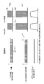
次に、図4に基づいて、顕微鏡本体100の構成について説明する。図4では、2種類のガルバノミラーを用いた共焦点蛍光顕微鏡の構成例を示している。顕微鏡本体100は、対象サンプルSに対して2つのガルバノミラーにより二次元にビーム走査を行なう。
[3. Configuration example of microscope system]
Next, the configuration of the microscope
光源200から射出された励起光は、レンズ等の光学系及び共役位置に設けられたピンホールを透過した後に、励起光を透過させるとともに蛍光を反射させるダイクロイックミラーを透過する。ダイクロイックミラーを透過した励起光は、レンズ等の光学系を透過し、測定サンプルのX方向の走査を制御するX方向ガルバノミラー120によりX座標が制御された後に、Y方向の走査を制御するY方向ガルバノミラー130によりY座標が制御され、対物レンズにより測定サンプルS上の所望のXY座標に集光される。
The excitation light emitted from the
測定サンプルから射出された蛍光は、Y方向ガルバノミラー130及びX方向ガルバノミラー120によって反射されて励起光と同じ経路をたどり、ダイクロイックミラーによって反射される。ダイクロイックミラーにより反射された蛍光は、共役位置に設けられたピンホールを透過した後、光電子増倍管(PMT)等の検出器110へと導光される。
The fluorescence emitted from the measurement sample is reflected by the Y-
ここで、測定サンプル上の集光位置を制御するために用いられる2つのガルバノミラーは、図4に模式的に示したように、ミラーに回転軸が接続されたものである。ガルバノミラー120,130は、入力された電圧の大きさによって回転軸の回転量が制御され、ミラー面が向いている角度を高速かつ高精度に変更することができる。 Here, the two galvanometer mirrors used for controlling the condensing position on the measurement sample are those in which a rotation axis is connected to the mirror as schematically shown in FIG. In the galvanometer mirrors 120 and 130, the amount of rotation of the rotating shaft is controlled by the magnitude of the input voltage, and the angle at which the mirror surface is facing can be changed at high speed and with high accuracy.
なお、図4では一光子励起の場合を示している。二光子励起の場合、ガルバノミラーおよびピンホールを通す必要は無いので、測定サンプルから射出された蛍光を、対物レンズの後段に設けられた光電子増倍管(PMT)等の検出器へと導光してもよい。 FIG. 4 shows the case of one-photon excitation. In the case of two-photon excitation, it is not necessary to pass through a galvanometer mirror and a pinhole, so that the fluorescence emitted from the measurement sample is guided to a detector such as a photomultiplier tube (PMT) provided after the objective lens. May be.
図4に示したようなレーザー走査型の顕微鏡では、2つのガルバノミラー120,130の動作方法の組み合わせにより、測定サンプルのXY平面を走査する際の励起光の移動の仕方が異なることとなる。以下では、図5を参照しながら、もっとも一般的な走査方式であるラスター・スキャン方式を利用した2次元画像の生成方法について説明する。ラスター・スキャン方式の場合は、水平方向にX方向のガルバノミラー120で走査し、折り返し近辺を除いた中心部で検出器110への戻り光をサンプリングして画像情報とする。
なお、以下の説明では、例えば図5に示した座標系が定義された測定サンプルSのサンプル平面において、X方向の走査を制御するガルバノミラー120の動作速度が、Y方向の走査を制御するガルバノミラー130の動作速度よりも早いものとする。
In the laser scanning microscope as shown in FIG. 4, the method of moving the excitation light when scanning the XY plane of the measurement sample differs depending on the combination of the operation methods of the two galvanometer mirrors 120 and 130. Hereinafter, a method for generating a two-dimensional image using a raster scanning method, which is the most common scanning method, will be described with reference to FIG. In the case of the raster scan method, scanning is performed by the
In the following description, for example, in the sample plane of the measurement sample S in which the coordinate system shown in FIG. 5 is defined, the operating speed of the
図5上段に示した図は、サンプル平面の左上部位を走査のスタート地点とした場合に、XY方向にどのように励起光が移動するかを模式的に示したものである。
ラスター・スキャン方式では、図5の測定サンプルSのサンプル平面に示したように、X方向ガルバノミラー120が回転して励起光がサンプル平面の左端から右端に向けてX方向に移動している期間に、蛍光の検出(画像の取得)が行われる。ラスター・スキャン方式では、X方向ガルバノミラー120が動作している期間は、Y方向ガルバノミラー130は静止している。
The diagram shown in the upper part of FIG. 5 schematically shows how the excitation light moves in the XY directions when the upper left part of the sample plane is the start point of scanning.
In the raster scan method, as shown in the sample plane of the measurement sample S in FIG. 5, the period in which the X
基本的には、励起光がサンプル平面の右端まで到達すると、蛍光の検出は中断され、X方向ガルバノミラー120は左端に対応する位置まで回転軸の回転角を変更する。この期間、Y方向ガルバノミラー130は、1ライン分だけY軸正方向にステップ移動する。このような動作をライン数だけ繰り返し、励起光がサンプル平面の右下まで到達すると、X方向ガルバノミラー120及びY方向ガルバノミラー130は、それぞれ回転軸を大きく回転させて走査のスタート地点に位置を戻すことで、1枚の2次元画像(フレーム)が生成されることとなる。
Basically, when the excitation light reaches the right end of the sample plane, the detection of fluorescence is interrupted, and the
このようなラスター・スキャン方式では、X方向ガルバノミラー120が動作している間はY方向ガルバノミラー130が静止しているため、生成される2次元画像を構成する単位(画像構成単位)の形状は、図5上段に示したような長方形となる。
In such a raster scan method, since the Y-
図5下段に示したグラフ図は、時間経過とともにY座標がどのように変化するかを示したタイミング・チャートである。1フレームの画像を得るために必要な時間をTframeとすると、この時間は、図5下段のタイミング・チャートからも明らかなように、以下の式11のように表される。ここで、下記式11において、Tscanは、走査周期を表しており、Nyは、Y方向のライン数を表しており、TY_allは、Y方向の戻り時間を表している。 The graph shown in the lower part of FIG. 5 is a timing chart showing how the Y coordinate changes with time. Assuming that the time required to obtain an image of one frame is T frame , this time is expressed by the following equation 11 as is apparent from the timing chart in the lower part of FIG. Here, in the following equation 11, T scan represents the scanning cycle, N y represents the number of lines in the Y direction, and T Y_all represents the return time in the Y direction.
Tframe=(Tscan)×Ny+TY_all ・・・(式11) T frame = (T scan ) × N y + T Y_all (Expression 11)
ここで、走査周期Tscanと、有効走査時間Teff及び帰引時間Tbackとの間には、以下の式12で表される関係がある。また、Y方向の戻り時間TY_allは、Y方向の1ライン移動時間をTyと表すこととすると、以下の式13のように表される。ここで、下記式12における帰引時間Tbackは、有効走査区間(例えば図5上段のサンプル平面において、X方向の実線で示した区間)の終わりから次の周期の有効走査区間の始まりまでの移動に要する合計時間を表している。 Here, there is a relationship represented by the following Expression 12 between the scanning cycle T scan , the effective scanning time T eff, and the retraction time T back . Further, the return time T Y_all in the Y direction is expressed as the following Expression 13, where T y represents the one-line movement time in the Y direction. Here, the retraction time T back in the following equation 12 is from the end of the effective scanning section (for example, the section indicated by the solid line in the X direction in the upper sample plane in FIG. 5) to the beginning of the effective scanning section of the next cycle. It represents the total time required for movement.
Teff=Tscan−Tback ・・・(式12)
TY_all=Ty×Ny ・・・(式13)
T eff = T scan −T back (Equation 12)
T Y_all = T y × N y ··· ( Equation 13)
例えば、X方向ガルバノミラー120の走査周波数Fscanが、7.8kHzである場合を考える。この場合、走査周期Tscanは、走査周波数Fscanの逆数として表されるため、Tscan=1/Fscan=1.28×10−4秒となる。また、このガルバノミラーの有効走査時間Teffが、走査効率に基づいて{走査周期Tscan×(1/3)}で表される場合、有効走査時間は、4.27×10−5秒となり、帰引時間Tbackは、1.28×10−4−4.27×10−5=8.53×10−5秒となる。
For example, consider a case where the scanning frequency F scan of the
また、Y方向ガルバノミラー130におけるY方向の戻り時間Tyが1×10⁻⁶秒であり、Y方向のライン数Nyが512ラインであったとすると、上記式11より、1フレームの撮影のために必要な時間Tframeは、6.62×10⁻²秒となる。フレーム・レートは、Tframeの逆数で表される値であるため、このような走査系では、Frame_rate=15.1(frame/s)となる。
Also, the return time T y Y direction in the Y-
図5に示すラスター・スキャン方式では、図5上段のサンプル平面に示したように、X方向ガルバノミラー120が回転して励起光がサンプル平面の左端から右端に向けてX方向に移動している期間において、有効走査時間Teffの間だけ光源200を発光させる。つまり、X方向の往復スキャンのうち、画像を取得する有効走査期間Teffのみ光源200をオンとし、有効走査期間Teff以外の期間、方向転換の期間は光源をOFFとする。この際、光源200のオン/オフは、50Hz〜10kHz程度の周波数で行われる。このため、上述したパルス波形P1による間欠駆動以外にも、有効走査期間Teffのみ光源200を発光させるために周期的な発光が行われるため、レーザーの平均パワーを低下させてピークパワーを高めることが可能である。
In the raster scan method shown in FIG. 5, as shown in the upper sample plane of FIG. 5, the
また、顕微鏡本体100が画像取得モードでない場合には、光源200はオフとされる。この際、光増幅器部240をオフにすることで光源200をオフにしても良いし、MLLD自体をオフにしてもよい。
When the microscope
[4.サンプリング周期と間欠発光周期の関係]
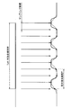
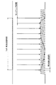
光子を検出する光電子増倍管(PMT)等の検出器110はアナログの素子であり、導入された光子を光電変換して電気信号(電流値、電圧値)へ変換する。変換された電気信号は、所定のサンプリング周期でA/D変換される。A/D変換された信号は、1ピクセルの画像情報に相当する。図6〜図8は、サンプリング周期とパルス波形P1による間欠発光の周期Tを示す特性図である。
[4. Relationship between sampling period and intermittent light emission period]
A
図6は、サンプリング周期が間欠発光周期Tよりも短い場合を示している。換言すれば、図6は、サンプリング周波数が間欠発光の周波数よりも高い場合を示している。図6の下段の特性において、実線の特性は検出器110による光電変換後の電気信号を表しており、破線はサンプリング値を結んだ特性を示している。この場合、発光が行われていないタイミング、すなわち励起されていないタイミングでサンプリングが行われる場合があるため、得られた画像は、隣接するピクセルにおいて、明暗が交互に現れるような画像(斑模様のような、いわゆる歯抜けした画像)となる。
FIG. 6 shows a case where the sampling period is shorter than the intermittent light emission period T. In other words, FIG. 6 shows a case where the sampling frequency is higher than the frequency of intermittent light emission. In the lower characteristic of FIG. 6, the solid line characteristic represents an electric signal after photoelectric conversion by the
図7は、サンプリング周期が間欠発光周期Tよりも長い場合を示している。換言すれば、図7は、サンプリング周波数が間欠発光の周波数よりも低い場合を示している。図6と同様に、実線の特性は検出器110による光電変換後の電気信号を表しており、破線はサンプリング値を結んだ特性を示している。この場合、光電変換後の電気信号には、サンプリング周波数よりも高い周波数の電気信号が含まれているため、本来は一定レベルの信号であるにも関わらず、様々な値がサンプリングされることになり、エイリアシングの影響により、正しい波形を再現することができない。このように、サンプリング周期と間欠発光周期Tが非同期の場合は、信号レベルが一定しない。また、サンプリング周期と間欠発光周期Tが同期していれば本来信号レベルは一定だが、非同期の場合は不必要な励起による退色が発生する。また、生体観察の場合、不必要な励起、光毒性により観察対象の細胞等が死滅するなどの弊害も生じる。
FIG. 7 shows a case where the sampling period is longer than the intermittent light emission period T. In other words, FIG. 7 shows a case where the sampling frequency is lower than the frequency of intermittent light emission. Similar to FIG. 6, the solid line characteristic represents an electrical signal after photoelectric conversion by the
図8は、サンプリング周期と間欠発光周期Tを一致させた場合を示している。つまり、図8は、サンプリング周波数が間欠発光の周波数と同一である場合を示している。図8においては、間欠発光周期Tのピークでサンプリングが行われるように位相も一致させている。このように、サンプリング周期と間欠発光周期Tが同期していれば、正しい信号が得られ、退色も最小限に抑えることができる。 FIG. 8 shows a case where the sampling period and the intermittent light emission period T are matched. That is, FIG. 8 shows a case where the sampling frequency is the same as the frequency of intermittent light emission. In FIG. 8, the phases are also matched so that sampling is performed at the peak of the intermittent light emission period T. Thus, if the sampling period and the intermittent light emission period T are synchronized, a correct signal can be obtained and fading can be minimized.
サンプリング周波数fsは、一例として100kHz〜10MHz程度である。基本的には、顕微鏡システム1000側の仕様からサンプリング周波数fsが定まり、サンプリング周波数fsに対して間欠発光の周波数を一致させる。一方、最初に間欠発光の周波数を定め、間欠発光の周波数に対してサンプリング周波数を一致させても良い。
As an example, the sampling frequency fs is about 100 kHz to 10 MHz. Basically, Sadamari the sampling frequency fs from the specification of the
なお、上記以外のパルス発光、走査ビームのオン/オフ信号、または画像取得のオン/オフ信号に関しても、A/D変換のサンプリング周期と同期していることが望ましいが、必ずしも同期していなくても良い。 It is desirable that the pulse emission other than the above, the on / off signal of the scanning beam, or the on / off signal of image acquisition is also synchronized with the sampling period of the A / D conversion, but is not necessarily synchronized. Also good.
サンプリング周期と間欠発光周期Tとを一致させるため、図1の光増幅器部240によるオン・オフの周期は、光電子増倍管(PMT)等の検出器110が検出した電気信号をA/D変換するA/D変換回路のサンプリング周期と同一とされる。つまり、SOAドライバ244によるオン・オフのクロックと同じものをそのままA/D変換回路へ入力することで、サンプリング周期と間欠発光周期Tとを確実に一致させることができる。これにより、サンプリング及び間欠発光に係る周波数及び位相を同一とすることができる。
To match the sampling period and the intermittent light emission period T, the period of the on and off by the
なお、図2に示したように、波長変換モジュール250から出力されたレーザー光L3は、間欠発光の発光期間内においてパルス状に発光する。図8では、このパルスが見えない程度のローパスフィルタ(図1に示すローパスフィルタ318)で処理した後の発光を示している。この際、後で詳細に説明するが、ローパスフィルタの帯域制限はサンプリング周波数の1/2以下とすることが望ましい。例えば、サンプリング周波数が1MHzの場合、ローパスフィルタの帯域制限は最大で500kHzとする。これにより、ナイキストのサンプリング定理を成立させることができる。従って、サンプリング周期と間欠駆動周期の位相ずれは許容されることになる。
As shown in FIG. 2, the laser light L3 output from the
[5.サンプリング周期と間欠駆動周期を一致させるための構成例]
次に、図1に基づいて、サンプリング周期と間欠駆動周期を一致させるための構成を説明する。図1に示すように、制御部300は、タイミングジェネレータ302、サンプリング信号発生部304、A/D変換部306、メモリ308、ガルバノビーム制御部310、DA変換部312、間欠発光信号発生部314、発振同期信号注入部316、ローパスフィルタ(LPF)318を有して構成される。
[5. Configuration example for matching sampling cycle and intermittent drive cycle]
Next, a configuration for matching the sampling period and the intermittent drive period will be described with reference to FIG. As shown in FIG. 1, the
図1に示すように、タイミングジェネレータ302はクロックCLKを発生し、サンプリング信号発生部304は、クロックCLKに基づいてサンプリング周波数fsのサンプリング信号を発生させる。また、間欠発光信号発生部314は、クロックCLKに基づいて間欠発光のための周期Tの間欠発光信号を発生させる。これにより、サンプリング信号発生部340が発生させるサンプリング信号と、間欠発光信号発生部314が発生させる間欠発光信号とを同期させることが可能となる。例えば、サンプリング信号発生部304がサンプリング周波数fsとしてクロックCLKをそのまま用い、間欠発光信号発生部314が間欠発光信号の周波数としてクロックCLKをそのまま用いることで、サンプリング周期と間欠発光周期Tとが一致する。
As shown in FIG. 1, the
ローパスフィルタ318には、検出器110が光電変換して得た電気信号が入力される。ローパスフィルタ318は、上述したように、ナイキストのサンプリング定理が成立するように入力された信号を帯域制限し、A/D変換部306へ出力する。A/D変換部306は、入力された信号をサンプリング周波数fsでA/D変換する。SOAドライバ244は間欠発光信号の周波数でレーザー光(パルス波形L1)をオン・オフし、間欠的なレーザー光(パルス波形L2)を出力する。
An electric signal obtained by photoelectric conversion by the
また、ガルバノビーム制御部310は、タイミングジェネレータ302からクロック信号CLKの入力を受け、ガルバノミラー120,130を制御するためのガルバノミラー制御信号を生成する。ガルバノミラー制御信号は、D/A変換部312によってD/A変換され、D/A変換されたガルバノミラー制御信号によってガルバノミラー120,130が制御される。これにより、ガルバノミラー120,130もクロックCLKに基づいて制御することができる。上述したようにラスター・スキャン方式では、有効走査時間Teffの間だけ光源200を発光させる。このため、間欠発光信号発生部314は、クロックCLKに基づいて、間欠発光信号をラスター・スキャンの有効走査時間Teffの間だけ発生させ、有効走査時間Teff以外の間は間欠発光信号をオフとする。同様に、サンプリング信号発生部304は、クロックCLKに基づいて、サンプリング信号を有効走査時間Teffの間だけ発生させる。従って、サンプリング信号及び間欠発光信号は、ガルバノミラーの動作周期に同期することになる。このように、サンプリング信号及び間欠発光信号を有効走査時間Teff以外の間はオフとすることによって、平均パワーを低下させることができ、ピークパワーを高めることができる。
The galvano
[6.ローパスフィルタの構成]
A/D変換部306の前段に設けられたローパスフィルタ318は、検出器(PMT)110の出力をナイキストのサンプリング定理を満たす周波数に帯域制限する。より具体的には、ローパスフィルタ318は、検出器110の出力をサンプリング周波数の1/2〜1/3の周波数に帯域制限する。例えば、サンプリング周波数が1GHzである場合、検出器110の出力は300〜500kHz程度に帯域制限される。サンプリング周波数が可変である場合には、ローパスフィルタ318の帯域もサンプリング周波数に比例して変更する。
[6. Configuration of low-pass filter]
A low-
検出器110の出力をナイキストのサンプリング定理を満たす周波数に帯域制限することで、サンプリング結果に不要な信号が含まれてしまうことを確実に抑止することができ、画像の再現性を確実に向上させることが可能となる。
By band-limiting the output of the
[7.レーザー光の発振光パルスとレーザー光の変調との同期]
次に、レーザー光の発振光パルスと間欠発光信号の周期との関係について説明する。本実施形態では、レーザー光の光発振パルスについても、タイミングジェネレータ302のクロックCLKと同期させることができる。
[7. Synchronization of laser light oscillation pulse and laser light modulation]
Next, the relationship between the oscillation light pulse of the laser light and the period of the intermittent light emission signal will be described. In the present embodiment, the laser oscillation pulse of the laser beam can also be synchronized with the clock CLK of the
モードロックレーザー部220から出射されるレーザー光の発振周波数は、光の速度と上述した外部共振器の行路長で決定される。タイミングジェネレータ302から注入する信号も共振器の周波数とほぼ同じとされるが、発振同期信号注入部316からの発信同期信号の注入によって、システムが有する位相情報を与えることで、システムが有する位相情報を外部共振器と同期させることができる。
The oscillation frequency of laser light emitted from the mode-locked
このため、発振同期信号注入部316は、タイミングジェネレータ302のクロック信号CLKに基づいて、クロックCLKと同期した発振同期信号をバイアスTeeのコンデンサに送る。この発振同期信号は、半導体レーザー222用のゲイン電流IgのAC成分として供給される。
Therefore, the oscillation synchronization
そして、クロックCLKと同期した発振同期信号が、半導体レーザー222用のゲイン電流IgのAC成分として供給されるため、半導体レーザー222から出射されるレーザー光の発振光パルスをクロックCLKと同期させることができる。
Since the oscillation synchronization signal synchronized with the clock CLK is supplied as the AC component of the gain current Ig for the
以上のように、発振同期信号注入部316から、クロックCLKに同期した発振同期信号が半導体レーザー222に供給される。これにより、半導体レーザー222から出射されるレーザー光の発振光パルスと、クロックCLKとを同期させることが可能となる。
As described above, the oscillation synchronization signal synchronized with the clock CLK is supplied from the oscillation synchronization
また、上述のように間欠発光信号発生部314は、クロックCLKに基づいて間欠発光のための間欠発光信号を発生させ、間欠発光信号によって光増幅器240を駆動させるので、光増幅器240がクロック信号CLKと同期してオン・オフ駆動され、クロックCLKと同期してレーザー光が変調される。従って、半導体レーザー222から出射されるレーザー光の発振光パルスと、レーザー光の変調とを同期させることができる。これにより、非常に高いパルス光周波数を有するレーザー光であっても、レーザー光の発振光パルスとレーザー光の変調とを容易に同期させることができ、所望の画像を取得することが可能となる。
Further, as described above, the intermittent light emission
なお、発振同期信号注入部316によるレーザー光の発振光パルスの同期は任意であり、同期を行わなくても良い。特にレーザー光の発振光パルスの周期と間欠発光信号の周期とが大きく相違している場合は、同期を行うことなく所望の画像を取得することができる。
Note that the synchronization of the oscillation light pulse of the laser beam by the oscillation synchronization
[8.光学的分解能とサンプリング周波数の関係]
レーザー走査顕微鏡の分解能は、励起光源の波長λ[m]に比例する光学的分解能によって決定される。光学的分解能doは、λ/2または0.61*λで見積もられるが、簡単のためにλ/2を使うと、λ=1000nmでは光学的分解能do=500nmとなる。光電変換素子の帯域に制約が無い場合、電気的な分解能deは、ビーム速度v[m/s]とサンプリング周波数fs[1/s]によって決定される。
[8. Relationship between optical resolution and sampling frequency]
The resolution of the laser scanning microscope is determined by the optical resolution proportional to the wavelength λ [m] of the excitation light source. The optical resolution do can be estimated by λ / 2 or 0.61 * λ. However, if λ / 2 is used for simplicity, the optical resolution do = 500 nm at λ = 1000 nm. When there is no restriction on the band of the photoelectric conversion element, the electrical resolution de is determined by the beam velocity v [m / s] and the sampling frequency fs [1 / s].
電気的な分解能deは、ナイキストのサンプリング定理により、サンプリング間隔[m]=v/fsの1/2になるので、電気的な分解能de=v/(2*fs)として計算できる。 The electrical resolution de is 1/2 of the sampling interval [m] = v / fs according to the Nyquist sampling theorem, and can be calculated as the electrical resolution de = v / (2 * fs).
ビーム速度v[m/s]は、走査ビームの往復周波数と走査範囲から計算できるので、代表的な数字として往復周波数500Hz、走査範囲1mmとして計算すると、1mmの範囲を周期2msの半分1msで走査することにより、v=1[m/s]となる。 The beam velocity v [m / s] can be calculated from the reciprocating frequency of the scanning beam and the scanning range. Therefore, when the reciprocating frequency is 500 Hz and the scanning range is 1 mm as a representative number, the 1 mm range is scanned at half a ms of 1 ms. By doing so, it becomes v = 1 [m / s].
この結果、電気的分解能deは、fs=1MHzではde=1[m/s]/(2*1E+6[1/2])=500nmとなり、これは光学的分解能doと一致する。 As a result, the electrical resolution de is de = 1 [m / s] / (2 * 1E + 6 [1/2]) = 500 nm at fs = 1 MHz, which matches the optical resolution do.
以上より、ビーム速度を10倍に速くする場合であっても、サンプリング周波数としては10MHzあれば十分であり、これ以上サンプリング周波数を高くするメリットは存在しないことがわかる。従って、前述した特許文献1からは、本実施形態で説明したような効果を得ることは困難であり、パルス発光に同期した高速サンプリングをしたとしても、分解能が向上することはなく、信号量を増やすことも困難である。 From the above, it can be seen that even when the beam speed is increased 10 times, a sampling frequency of 10 MHz is sufficient, and there is no merit of increasing the sampling frequency any more. Therefore, from Patent Document 1 described above, it is difficult to obtain the effect as described in the present embodiment. Even if high-speed sampling synchronized with pulse emission is performed, the resolution is not improved, and the signal amount is reduced. It is also difficult to increase.
以上説明したように本実施形態によれば、光源200からのレーザー光を間欠発光させ、間欠発光の周期と検出器110から得られた画像の電気信号のサンプリング周期を一致させるようにした。これにより、斑模様、歯抜けした画像が得られることを確実に抑止することができ、また、エイリアシングの影響により正しい波形が再現できなくなることを確実に抑止できる。更に、レーザー光の不必要な励起を抑えることができ、光毒性により観察対象の細胞等が死滅するなどの弊害も抑止することができる。
As described above, according to the present embodiment, the laser light from the
以上、添付図面を参照しながら本開示の好適な実施形態について詳細に説明したが、本開示の技術的範囲はかかる例に限定されない。本開示の技術分野における通常の知識を有する者であれば、特許請求の範囲に記載された技術的思想の範疇内において、各種の変更例または修正例に想到し得ることは明らかであり、これらについても、当然に本開示の技術的範囲に属するものと了解される。 The preferred embodiments of the present disclosure have been described in detail above with reference to the accompanying drawings, but the technical scope of the present disclosure is not limited to such examples. It is obvious that a person having ordinary knowledge in the technical field of the present disclosure can come up with various changes or modifications within the scope of the technical idea described in the claims. Of course, it is understood that it belongs to the technical scope of the present disclosure.
なお、以下のような構成も本開示の技術的範囲に属する。
(1)所定の周波数のレーザー光を出射するモードロックレーザー部と、
前記モードロックレーザー部から出射されるレーザー光を所定の間欠発光周期で間欠発光させる間欠発光部と、
間欠発光された前記レーザー光を受けて対象物から励起した蛍光体を電気信号に変換する検出器と、
前記電気信号を前記間欠発光周期と同期したサンプリング周期でサンプリングするA/D変換部と、
を備える、レーザー走査型顕微鏡システム。
(2)前記サンプリング及び前記間欠発光に係る周波数及び位相が同一である、前記(1)に記載のレーザー走査型顕微鏡システム。
(3)前記モードロックレーザー部は、二光子励起のための前記レーザー光を出射する、前記(1)に記載のレーザー走査型顕微鏡システム。
(4)前記A/D変換部に対して前記サンプリング周期を与えるサンプリング信号と、前記間欠発光部に対して前記間欠発光周期を与える間欠発光信号とが同一の信号である、前記(1)に記載のレーザー走査型顕微鏡システム。
(5)前記A/D変換部に対して前記サンプリング周期を与えるサンプリング信号を発生させるサンプリング信号発生部と、
前記間欠発光部に対して前記間欠発光周期を与える間欠発光信号を発生させる間欠発光信号発生部と、を更に備え、
前記サンプリング信号と前記間欠発光信号とを同一のクロックに基づいて発生させる、前記(1)に記載のレーザー走査型顕微鏡システム。
(6)前記モードロックレーザー部又は前記間欠発光部は、前記レーザー光を所定の有効発光期間のみ前記対象物に入射させる、前記(1)に記載のレーザー走査型顕微鏡システム。
(7)前記レーザー光を前記対象物の表面の第1の方向へ走査する第1のガルバノミラーと、
前記レーザー光を前記対象物の表面の前記第1の方向と直交する第2の方向へ走査する第2のガルバノミラーと、
前記第1及び第2のガルバノミラーを制御するガルバノミラー制御部と、を備え、
前記ガルバノミラー制御部は、前記第1の方向への走査が完了すると、前記第1の方向の始点位置に前記レーザー光を戻すとともに、前記レーザー光の1ライン分だけ前記第2の方向への走査を行い、その後、再び前記第1の方向への走査を行い、
前記有効発光期間は、前記第1の方向へ走査を行う期間の少なくとも一部である、前記(6)に記載のレーザー走査型顕微鏡システム。
(8)前記検出器から出力された前記電気信号を帯域制限して前記A/D変換部へ入力するローパスフィルタを備え、
前記ローパスフィルタは、前記サンプリングの周波数に対してナイキストのサンプリング定理が成立するように前記帯域制限を行う、前記(1)に記載のレーザー走査型顕微鏡システム。
(9)前記ローパスフィルタは、前記サンプリングの周波数の1/2以下となるように前記帯域制限を行う、前記(8)に記載のレーザー走査型顕微鏡システム。
The following configurations also belong to the technical scope of the present disclosure.
(1) a mode-locked laser unit that emits laser light of a predetermined frequency;
An intermittent light emitting unit that intermittently emits laser light emitted from the mode-locked laser unit at a predetermined intermittent light emission period;
A detector that converts the phosphor excited from the object by receiving the intermittently emitted laser light into an electrical signal;
An A / D converter that samples the electrical signal at a sampling period synchronized with the intermittent light emission period;
A laser scanning microscope system.
(2) The laser scanning microscope system according to (1), wherein the frequency and phase related to the sampling and the intermittent light emission are the same.
(3) The laser scanning microscope system according to (1), wherein the mode-locked laser unit emits the laser light for two-photon excitation.
(4) In (1), the sampling signal that gives the sampling period to the A / D converter and the intermittent light emission signal that gives the intermittent light emission period to the intermittent light emission part are the same signal. The laser scanning microscope system described.
(5) a sampling signal generator for generating a sampling signal for giving the sampling period to the A / D converter;
An intermittent light emission signal generating unit that generates an intermittent light emission signal that gives the intermittent light emission period to the intermittent light emission unit, and
The laser scanning microscope system according to (1), wherein the sampling signal and the intermittent light emission signal are generated based on the same clock.
(6) The laser scanning microscope system according to (1), wherein the mode-locked laser unit or the intermittent light emitting unit causes the laser light to be incident on the object only during a predetermined effective light emission period.
(7) a first galvanometer mirror that scans the laser beam in a first direction of the surface of the object;
A second galvanometer mirror that scans the laser light in a second direction orthogonal to the first direction of the surface of the object;
A galvanometer mirror controller that controls the first and second galvanometer mirrors,
When the scanning in the first direction is completed, the galvanomirror control unit returns the laser beam to the start position in the first direction and moves the laser beam in the second direction by one line of the laser beam. Scan, and then scan again in the first direction,
The laser scanning microscope system according to (6), wherein the effective light emission period is at least part of a period during which scanning is performed in the first direction.
(8) A low-pass filter that limits the band of the electrical signal output from the detector and inputs the electrical signal to the A / D converter,
The laser scanning microscope system according to (1), wherein the low-pass filter performs the band limitation so that a Nyquist sampling theorem is established with respect to the sampling frequency.
(9) The laser scanning microscope system according to (8), wherein the low-pass filter performs the band limitation so as to be equal to or less than ½ of the sampling frequency.
1000 顕微鏡システム
110 検出器
220 モードロックレーザー部
240 光増幅器部(SOA部)
306 A/D変換部
1000
306 A / D converter
Claims (9)
前記モードロックレーザー部から出射されるレーザー光を増幅するとともに、前記所定の周波数に対応する周期よりも長い所定の間欠発光周期で間欠発光させる間欠発光部と、
間欠発光された前記レーザー光を受けて対象物から励起した蛍光体を電気信号に変換する検出器と、
前記電気信号を前記間欠発光周期と同期したサンプリング周期でサンプリングするA/D変換部と、
を備える、レーザー走査型顕微鏡システム。 A mode-locked laser unit that emits laser light of a predetermined frequency;
An intermittent light emitting unit that amplifies laser light emitted from the mode-locked laser unit and emits light intermittently at a predetermined intermittent light emission period longer than a period corresponding to the predetermined frequency;
A detector that converts the phosphor excited from the object by receiving the intermittently emitted laser light into an electrical signal;
An A / D converter that samples the electrical signal at a sampling period synchronized with the intermittent light emission period;
A laser scanning microscope system.
前記間欠発光部に対して前記間欠発光周期を与える間欠発光信号を発生させる間欠発光信号発生部と、を更に備え、
前記サンプリング信号と前記間欠発光信号とを同一のクロックに基づいて発生させる、請求項1〜4のいずれかに記載のレーザー走査型顕微鏡システム。 A sampling signal generator for generating a sampling signal for giving the sampling period to the A / D converter;
An intermittent light emission signal generating unit that generates an intermittent light emission signal that gives the intermittent light emission period to the intermittent light emission unit, and
The laser scanning microscope system according to claim 1, wherein the sampling signal and the intermittent light emission signal are generated based on the same clock.
前記レーザー光を前記対象物の表面の前記第1の方向と直交する第2の方向へ走査する第2のガルバノミラーと、
前記第1及び第2のガルバノミラーを制御するガルバノミラー制御部と、を備え、
前記ガルバノミラー制御部は、前記第1の方向への走査が完了すると、前記第1の方向の始点位置に前記レーザー光を戻すとともに、前記レーザー光の1ライン分だけ前記第2の方向への走査を行い、その後、再び前記第1の方向への走査を行い、
前記有効発光期間は、前記第1の方向へ走査を行う期間の少なくとも一部である、請求項6に記載のレーザー走査型顕微鏡システム。 A first galvanometer mirror that scans the laser light in a first direction of the surface of the object;
A second galvanometer mirror that scans the laser light in a second direction orthogonal to the first direction of the surface of the object;
A galvanometer mirror controller that controls the first and second galvanometer mirrors,
When the scanning in the first direction is completed, the galvanomirror control unit returns the laser beam to the start position in the first direction and moves the laser beam in the second direction by one line of the laser beam. Scan, and then scan again in the first direction,
The laser scanning microscope system according to claim 6, wherein the effective light emission period is at least a part of a period during which scanning is performed in the first direction.
前記ローパスフィルタは、前記サンプリングの周波数に対してナイキストのサンプリング定理が成立するように前記帯域制限を行う、請求項1に記載のレーザー走査型顕微鏡システム。 A low-pass filter that limits the band of the electrical signal output from the detector and inputs the electrical signal to the A / D converter;
The laser scanning microscope system according to claim 1, wherein the low-pass filter performs the band limitation so that a Nyquist sampling theorem is established with respect to the sampling frequency.
Priority Applications (3)
| Application Number | Priority Date | Filing Date | Title |
|---|---|---|---|
| JP2013113572A JP6281193B2 (en) | 2013-05-30 | 2013-05-30 | Laser scanning microscope system |
| US14/279,934 US9551664B2 (en) | 2013-05-30 | 2014-05-16 | Laser scanning microscope system |
| CN201410223168.9A CN104215612B (en) | 2013-05-30 | 2014-05-23 | Laser scanning microscope system |
Applications Claiming Priority (1)
| Application Number | Priority Date | Filing Date | Title |
|---|---|---|---|
| JP2013113572A JP6281193B2 (en) | 2013-05-30 | 2013-05-30 | Laser scanning microscope system |
Publications (3)
| Publication Number | Publication Date |
|---|---|
| JP2014232241A JP2014232241A (en) | 2014-12-11 |
| JP2014232241A5 JP2014232241A5 (en) | 2016-03-17 |
| JP6281193B2 true JP6281193B2 (en) | 2018-02-21 |
Family
ID=51984049
Family Applications (1)
| Application Number | Title | Priority Date | Filing Date |
|---|---|---|---|
| JP2013113572A Expired - Fee Related JP6281193B2 (en) | 2013-05-30 | 2013-05-30 | Laser scanning microscope system |
Country Status (3)
| Country | Link |
|---|---|
| US (1) | US9551664B2 (en) |
| JP (1) | JP6281193B2 (en) |
| CN (1) | CN104215612B (en) |
Families Citing this family (8)
| Publication number | Priority date | Publication date | Assignee | Title |
|---|---|---|---|---|
| US8236574B2 (en) * | 2010-03-01 | 2012-08-07 | Quanterix Corporation | Ultra-sensitive detection of molecules or particles using beads or other capture objects |
| JP2015161719A (en) * | 2014-02-26 | 2015-09-07 | ソニー株式会社 | laser scanning microscope system and sampling device |
| JP6550673B2 (en) * | 2015-04-03 | 2019-07-31 | 国立大学法人 東京大学 | Photoluminescence lifetime measuring apparatus and measuring method |
| JP2017049447A (en) * | 2015-09-02 | 2017-03-09 | オリンパス株式会社 | Laser microscope and microscope observation method |
| JP6651768B2 (en) * | 2015-09-28 | 2020-02-19 | 株式会社ニコン | Pattern drawing equipment |
| US10473908B2 (en) * | 2017-04-21 | 2019-11-12 | Shimadzu Corporation | Optical observation device |
| TWI714378B (en) * | 2019-12-04 | 2020-12-21 | 國立臺灣大學 | A large-angle optical raster scanning system for high speed deep tissue imaging |
| CN112987273B (en) * | 2021-04-15 | 2023-08-29 | 南方科技大学 | Fluorescence excitation block light source and fluorescence microscope |
Family Cites Families (25)
| Publication number | Priority date | Publication date | Assignee | Title |
|---|---|---|---|---|
| US4794598A (en) * | 1986-07-18 | 1988-12-27 | The Board Of Trustees Of The Leland Stanford Junior University | Synchronously pumped ring fiber Raman laser |
| US5252834A (en) * | 1990-11-13 | 1993-10-12 | Union Oil Company Of California | Pulsed and gated multi-mode microspectrophotometry device and method |
| US5982535A (en) * | 1997-08-07 | 1999-11-09 | Marine Biological Laboratory | Centrifuge microscope capable of realizing polarized light observation |
| JP4667571B2 (en) * | 1999-09-24 | 2011-04-13 | オリンパス株式会社 | Laser scanning microscope |
| US20010015411A1 (en) * | 1999-09-24 | 2001-08-23 | Yasuo Ohdaira | Laser scanning microscope |
| JP2001188902A (en) * | 2000-01-04 | 2001-07-10 | Konica Corp | Radiation image reader |
| DE10211387B4 (en) * | 2001-03-15 | 2020-03-26 | Omron Corp. | Sensor using radiation pulses |
| JP4930742B2 (en) * | 2001-03-29 | 2012-05-16 | 株式会社トプコン | Position detection device |
| JP4912545B2 (en) * | 2001-07-13 | 2012-04-11 | オリンパス株式会社 | Confocal laser scanning microscope |
| JP4175833B2 (en) * | 2002-05-23 | 2008-11-05 | オリンパス株式会社 | Laser microscope |
| DK2305172T3 (en) * | 2003-03-28 | 2016-08-22 | Inguran Llc | DEVICE AND PROCEDURES TO PROVIDE SEXUAL ANIMAL SEED |
| DE102005047884A1 (en) * | 2005-10-06 | 2007-04-26 | Leica Microsystems Cms Gmbh | Scanning microscope and scanning method with a scanning microscope |
| CN100541204C (en) * | 2006-08-11 | 2009-09-16 | 中国科学院力学研究所 | A kind of measurement mechanism of fluid channel velocity distribution and measuring method |
| JP2009229715A (en) * | 2008-03-21 | 2009-10-08 | Olympus Corp | Microscope |
| DE102009055993B4 (en) * | 2009-11-26 | 2016-06-02 | Leica Microsystems Cms Gmbh | A method of inspecting an object with the aid of a microscope and a microscope-like device for examining an object |
| US8630322B2 (en) * | 2010-03-01 | 2014-01-14 | Board Of Trustees Of Michigan State University | Laser system for output manipulation |
| JP5771371B2 (en) * | 2010-07-22 | 2015-08-26 | オリンパス株式会社 | Laser scanning microscope |
| JP5589671B2 (en) * | 2010-08-20 | 2014-09-17 | ソニー株式会社 | Laser apparatus, laser amplification modulation method. |
| JP2012059343A (en) * | 2010-09-13 | 2012-03-22 | Sony Corp | Recording device |
| JP2012185888A (en) * | 2011-03-07 | 2012-09-27 | Sony Corp | Recording device |
| DE102011105181A1 (en) * | 2011-06-17 | 2012-12-20 | Leica Microsystems Cms Gmbh | Microscope and method for imaging fluorescence microscopy |
| CN202814861U (en) * | 2012-07-31 | 2013-03-20 | 苏州微清医疗器械有限公司 | Multifunctional biomedical microscope |
| JP5602817B2 (en) * | 2012-11-07 | 2014-10-08 | 住友大阪セメント株式会社 | Optical pulse laser device and optical pulse laser generation method |
| US10180402B2 (en) * | 2012-12-14 | 2019-01-15 | Sri International | Method and apparatus for conducting automated integrated circuit analysis |
| US9778193B2 (en) * | 2013-08-22 | 2017-10-03 | Kinetic River Corp. | Methods and apparatuses for label-free particle analysis |
-
2013
- 2013-05-30 JP JP2013113572A patent/JP6281193B2/en not_active Expired - Fee Related
-
2014
- 2014-05-16 US US14/279,934 patent/US9551664B2/en not_active Expired - Fee Related
- 2014-05-23 CN CN201410223168.9A patent/CN104215612B/en not_active Expired - Fee Related
Also Published As
| Publication number | Publication date |
|---|---|
| US20140353521A1 (en) | 2014-12-04 |
| JP2014232241A (en) | 2014-12-11 |
| US9551664B2 (en) | 2017-01-24 |
| CN104215612B (en) | 2018-07-31 |
| CN104215612A (en) | 2014-12-17 |
Similar Documents
| Publication | Publication Date | Title |
|---|---|---|
| JP6281193B2 (en) | Laser scanning microscope system | |
| JP2015161719A (en) | laser scanning microscope system and sampling device | |
| JP5776992B2 (en) | STED microscopy, STED fluorescence correlation spectroscopy, and STED fluorescence microscope for pulse excitation, continuous deexcitation, and gate recording of spontaneous emission fluorescence | |
| JP2823970B2 (en) | Near-field scanning optical microscope | |
| WO2006061947A1 (en) | Fluorescence microscope and observation method | |
| JP2003515162A (en) | How to understand the fluorescence phenomenon inside the microscope | |
| US20050078296A1 (en) | Imaging device for recording depth | |
| US20180246309A1 (en) | Scan-based imaging with variable scan speed using predictions of region-of-interest positions | |
| JP2009229715A (en) | Microscope | |
| CN105527265A (en) | Laser pump time resolution up-conversion luminescence living imaging system | |
| US11944448B2 (en) | Adaptive illumination apparatus, method, and applications | |
| JP7064315B2 (en) | Photodetector and laser scanning microscope | |
| JPH0670613B2 (en) | Optical waveform measuring device | |
| JP4407423B2 (en) | Laser microscope | |
| CN206074450U (en) | Two Photon Fluorescence and clinical treatment device | |
| Chen et al. | Widefield multifrequency fluorescence lifetime imaging using a two‐tap complementary metal‐oxide semiconductor camera with lateral electric field charge modulators | |
| CN113504634B (en) | Intelligent high-speed scanning method and device for point scanning long-life fluorescence microscopic imaging | |
| JP2680398B2 (en) | Optical waveform measurement device | |
| Nichols et al. | Autofluorescence lifetime imaging | |
| US20120292529A1 (en) | Stroboscopic optical image mapping system | |
| JP2012058019A (en) | Light detection device, light detection method, microscope, and endoscope | |
| Karpf et al. | Frequency Doubled High Speed Fluorescence Lifetime Imaging | |
| WO2021166523A1 (en) | Distance measurement device and distance measurement method | |
| JP2656106B2 (en) | Optical waveform measurement device | |
| KR102430669B1 (en) | Apparatus and method for in vitro diagnostic device by measuring fluorescence lifetime |
Legal Events
| Date | Code | Title | Description |
|---|---|---|---|
| A521 | Written amendment |
Free format text: JAPANESE INTERMEDIATE CODE: A523 Effective date: 20160202 |
|
| A621 | Written request for application examination |
Free format text: JAPANESE INTERMEDIATE CODE: A621 Effective date: 20160202 |
|
| A977 | Report on retrieval |
Free format text: JAPANESE INTERMEDIATE CODE: A971007 Effective date: 20161209 |
|
| A131 | Notification of reasons for refusal |
Free format text: JAPANESE INTERMEDIATE CODE: A131 Effective date: 20161220 |
|
| A521 | Written amendment |
Free format text: JAPANESE INTERMEDIATE CODE: A523 Effective date: 20170210 |
|
| A02 | Decision of refusal |
Free format text: JAPANESE INTERMEDIATE CODE: A02 Effective date: 20170718 |
|
| A521 | Written amendment |
Free format text: JAPANESE INTERMEDIATE CODE: A523 Effective date: 20171010 |
|
| A911 | Transfer to examiner for re-examination before appeal (zenchi) |
Free format text: JAPANESE INTERMEDIATE CODE: A911 Effective date: 20171017 |
|
| TRDD | Decision of grant or rejection written | ||
| A01 | Written decision to grant a patent or to grant a registration (utility model) |
Free format text: JAPANESE INTERMEDIATE CODE: A01 Effective date: 20171226 |
|
| A61 | First payment of annual fees (during grant procedure) |
Free format text: JAPANESE INTERMEDIATE CODE: A61 Effective date: 20180108 |
|
| R151 | Written notification of patent or utility model registration |
Ref document number: 6281193 Country of ref document: JP Free format text: JAPANESE INTERMEDIATE CODE: R151 |
|
| LAPS | Cancellation because of no payment of annual fees |