JP6273216B2 - Capacitor leakage compensation for PLL loop filter capacitors - Google Patents
Capacitor leakage compensation for PLL loop filter capacitors Download PDFInfo
- Publication number
- JP6273216B2 JP6273216B2 JP2014560101A JP2014560101A JP6273216B2 JP 6273216 B2 JP6273216 B2 JP 6273216B2 JP 2014560101 A JP2014560101 A JP 2014560101A JP 2014560101 A JP2014560101 A JP 2014560101A JP 6273216 B2 JP6273216 B2 JP 6273216B2
- Authority
- JP
- Japan
- Prior art keywords
- capacitor
- charge pump
- voltage
- current
- coupled
- Prior art date
- Legal status (The legal status is an assumption and is not a legal conclusion. Google has not performed a legal analysis and makes no representation as to the accuracy of the status listed.)
- Expired - Fee Related
Links
- 239000003990 capacitor Substances 0.000 title claims description 222
- 238000001514 detection method Methods 0.000 claims description 14
- 238000000034 method Methods 0.000 claims description 13
- 239000004020 conductor Substances 0.000 claims description 9
- 238000001914 filtration Methods 0.000 claims description 2
- 230000008878 coupling Effects 0.000 claims 2
- 238000010168 coupling process Methods 0.000 claims 2
- 238000005859 coupling reaction Methods 0.000 claims 2
- 238000010586 diagram Methods 0.000 description 18
- 239000010409 thin film Substances 0.000 description 11
- 239000010408 film Substances 0.000 description 9
- 230000005669 field effect Effects 0.000 description 7
- 230000007423 decrease Effects 0.000 description 3
- 239000002184 metal Substances 0.000 description 3
- 230000008569 process Effects 0.000 description 3
- 239000004065 semiconductor Substances 0.000 description 3
- 230000002238 attenuated effect Effects 0.000 description 2
- 230000003247 decreasing effect Effects 0.000 description 2
- 229910044991 metal oxide Inorganic materials 0.000 description 2
- 150000004706 metal oxides Chemical class 0.000 description 2
- 230000006978 adaptation Effects 0.000 description 1
- 230000002411 adverse Effects 0.000 description 1
- 230000002349 favourable effect Effects 0.000 description 1
- 239000000463 material Substances 0.000 description 1
- 238000012986 modification Methods 0.000 description 1
- 230000004048 modification Effects 0.000 description 1
- 230000010076 replication Effects 0.000 description 1
- 230000004044 response Effects 0.000 description 1
Images


Classifications
-
- H—ELECTRICITY
- H03—ELECTRONIC CIRCUITRY
- H03L—AUTOMATIC CONTROL, STARTING, SYNCHRONISATION OR STABILISATION OF GENERATORS OF ELECTRONIC OSCILLATIONS OR PULSES
- H03L7/00—Automatic control of frequency or phase; Synchronisation
- H03L7/06—Automatic control of frequency or phase; Synchronisation using a reference signal applied to a frequency- or phase-locked loop
- H03L7/08—Details of the phase-locked loop
- H03L7/085—Details of the phase-locked loop concerning mainly the frequency- or phase-detection arrangement including the filtering or amplification of its output signal
- H03L7/089—Details of the phase-locked loop concerning mainly the frequency- or phase-detection arrangement including the filtering or amplification of its output signal the phase or frequency detector generating up-down pulses
- H03L7/0891—Details of the phase-locked loop concerning mainly the frequency- or phase-detection arrangement including the filtering or amplification of its output signal the phase or frequency detector generating up-down pulses the up-down pulses controlling source and sink current generators, e.g. a charge pump
-
- H—ELECTRICITY
- H03—ELECTRONIC CIRCUITRY
- H03L—AUTOMATIC CONTROL, STARTING, SYNCHRONISATION OR STABILISATION OF GENERATORS OF ELECTRONIC OSCILLATIONS OR PULSES
- H03L7/00—Automatic control of frequency or phase; Synchronisation
- H03L7/06—Automatic control of frequency or phase; Synchronisation using a reference signal applied to a frequency- or phase-locked loop
- H03L7/08—Details of the phase-locked loop
- H03L7/085—Details of the phase-locked loop concerning mainly the frequency- or phase-detection arrangement including the filtering or amplification of its output signal
- H03L7/093—Details of the phase-locked loop concerning mainly the frequency- or phase-detection arrangement including the filtering or amplification of its output signal using special filtering or amplification characteristics in the loop
Landscapes
- Stabilization Of Oscillater, Synchronisation, Frequency Synthesizers (AREA)
Description
本開示は、位相ロックループ(PLL)内のキャパシタ漏れ補償回路に関する。 The present disclosure relates to a capacitor leakage compensation circuit in a phase locked loop (PLL).
位相ロックループ(PLL)のループフィルタは、比較的大きい静電容量を有するキャパシタを伴い得る。このキャパシタを集積回路の形で実現すると、集積回路上で、望ましくないほど大量の面積を消費し得る。キャパシタは、様々なやり方で実装することができる。キャパシタが、あるやり方で実装される場合、キャパシタは、比較的大量の集積回路面積を占めるが、わずかにしか漏れない。一方、キャパシタが別のやり方で実装される場合、キャパシタは、集積回路面積のうち比較的少ない量しか占めないが、より大幅に漏れる。いくつかのケースでは、キャパシタは、比較的小さいが漏れのあるキャパシタとして実装されるが、その場合、キャパシタ漏れ補償回路が設けられる。キャパシタ漏れ補償回路は、「レプリカ」キャパシタと呼ばれる、漏れキャパシタの小型バージョンを含む。より大型のキャパシタおよびレプリカキャパシタが、電圧に応じてどの程度漏れるかは同じであり、レプリカキャパシタが、大きい方のキャパシタよりもどれだけ小さいかに比例して、より少なく漏れるだけである。キャパシタ漏れ補償回路は、ループフィルタが動作中のときにループフィルタの漏れキャパシタ両端間の電圧と同じである、レプリカキャパシタ両端間の電圧を維持するように動作する。キャパシタ漏れ補償回路は、ただし、レプリカキャパシタを通って漏れる電流を検出する。ループフィルタ内のレプリカキャパシタと漏れキャパシタとの間のサイズの関係が知られているので、補償回路は、検出された量の漏れ電流の倍数を、ループフィルタ内の漏れキャパシタ上へ供給するように動作する。理想的には、この補償電流の大きさは、ループフィルタの漏れキャパシタから漏れる電流の大きさと同じである。そのようなキャパシタ漏れ電流補償回路により、ループフィルタのキャパシタは、比較的漏れがある、より小さいタイプのキャパシタとして実装され、そうすることによって、比較的漏れのない、より大きいタイプのキャパシタを使ってループフィルタが実装された場合にループフィルタが有するはずのサイズと比較して、集積回路面積を節約する。消費される集積回路面積の全体的量、電流消費の全体的量、および漏れキャパシタと補償回路を組み合わせた性能は、より大きいがより漏れのないキャパシタでループフィルタが実装されている場合、集積回路面積の代替量、電流消費、およびループフィルタの性能にとって好ましくなるべきである。 A phase-locked loop (PLL) loop filter may involve a capacitor having a relatively large capacitance. Implementation of this capacitor in the form of an integrated circuit can consume an undesirably large amount of area on the integrated circuit. The capacitor can be implemented in various ways. If the capacitor is implemented in some way, it occupies a relatively large amount of integrated circuit area but leaks only slightly. On the other hand, if the capacitor is implemented differently, it occupies a relatively small amount of the integrated circuit area but leaks significantly more. In some cases, the capacitor is implemented as a relatively small but leaky capacitor, in which case a capacitor leakage compensation circuit is provided. The capacitor leakage compensation circuit includes a small version of the leakage capacitor, referred to as a “replica” capacitor. The larger capacitor and replica capacitor will leak the same depending on the voltage, and the replica capacitor will only leak less in proportion to how small the larger capacitor is. The capacitor leakage compensation circuit operates to maintain a voltage across the replica capacitor that is the same as the voltage across the leakage capacitor of the loop filter when the loop filter is in operation. The capacitor leakage compensation circuit, however, detects the current leaking through the replica capacitor. Since the size relationship between the replica capacitor and the leakage capacitor in the loop filter is known, the compensation circuit supplies a multiple of the detected amount of leakage current onto the leakage capacitor in the loop filter. Operate. Ideally, the magnitude of this compensation current is the same as the current leaking from the leakage capacitor of the loop filter. With such a capacitor leakage current compensation circuit, the capacitor of the loop filter is implemented as a relatively leaky, smaller type capacitor, thereby using a relatively leak-free, larger type capacitor. Saves integrated circuit area compared to the size that the loop filter would have if the loop filter was implemented. The total amount of integrated circuit area consumed, the total amount of current consumption, and the combined performance of the leakage capacitor and the compensation circuit, the integrated circuit when the loop filter is implemented with a larger but less leakage capacitor It should be favorable for area alternatives, current consumption, and loop filter performance.
キャパシタ漏れ補償回路の第1の例が、米国特許第6,956,417号の図10で記載されている。このキャパシタ漏れ補償回路190は、位相検出器、電荷ポンプ、ループフィルタ、電圧制御発振器、およびループ分割器を伴う位相ロックループの一部であり得る。抵抗器RREFおよびキャパシタC1が、ループフィルタを構成する。キャパシタC1は、漏れキャパシタである。キャパシタC4は、レプリカキャパシタである。電圧VCは、漏れキャパシタ両端間の電圧である。キャパシタ漏れ補償回路190は、この電圧を検知し、この同じノードVC上へ、補償電流を折返し供給する。この回路は、漏れキャパシタ自体の上の電圧を検知するので、「直接検知」回路と呼ばれることがあるものの例である。
A first example of a capacitor leakage compensation circuit is described in FIG. 10 of US Pat. No. 6,956,417. This capacitor
キャパシタ漏れ補償回路の第2の例が、米国特許第6,963,232号の図4で記載されている。参照番号54は、漏れキャパシタを識別する。電流57は、キャパシタ54を通って漏れる電流である。キャパシタ59は、レプリカキャパシタである。漏れ補償回路39は、漏れキャパシタ両端間の電圧を、VCO42の入力において間接的に検知し、この電圧をレプリカキャパシタ両端間にかけ、レプリカキャパシタを通って漏れる電流70を検出し、検出された漏れ電流の倍数を、補償電流58の形で、ノード67上へ供給する。補償電流58は、キャパシタ54を通ってグラウンドに漏れる電流57を補償する。この回路は、漏れ補償回路が漏れキャパシタ上の電圧を間接的に検知する、「間接検知」の例である。
A second example of a capacitor leakage compensation circuit is described in FIG. 4 of US Pat. No. 6,963,232.
位相ロックループ(PLL)は、位相周波数検出器(PFD)、電荷ポンプ(CP)、ループフィルタ、電圧制御発振器(VCO)、ループ分割器、およびキャパシタ漏れ補償回路を含む。電荷ポンプは、電流制御部分および出力部分を含む。出力部分は、PFDから制御信号を受け、それに応答して、正電流パルスおよび負電流パルスを、電荷ポンプ出力ノードを介してループフィルタに出力する。電流制御部分は、正電流パルスの大きさと負電流パルスの大きさが同じになるように、出力部分を制御する。電流制御部分内には、本明細書において「電荷ポンプ出力電圧レプリカノード」(CPOVRN)と呼ばれるノードがある。電荷ポンプ出力ノード上の電圧のレプリカが、CPOVRN上に存在する。一例では、電流制御部分内の演算増幅器は、このCPOVRN上の電圧を、電荷ポンプ出力ノード上の電圧とほぼ等しく保つように動作する。 The phase locked loop (PLL) includes a phase frequency detector (PFD), a charge pump (CP), a loop filter, a voltage controlled oscillator (VCO), a loop divider, and a capacitor leakage compensation circuit. The charge pump includes a current control portion and an output portion. The output portion receives a control signal from the PFD, and in response, outputs a positive current pulse and a negative current pulse to the loop filter via the charge pump output node. The current control portion controls the output portion so that the magnitude of the positive current pulse and the magnitude of the negative current pulse are the same. Within the current control portion is a node referred to herein as a “charge pump output voltage replica node” (CPOVRN). A replica of the voltage on the charge pump output node is present on CPOVRN. In one example, an operational amplifier in the current control portion operates to keep this voltage on CPOVRN approximately equal to the voltage on the charge pump output node.
ループフィルタは、電荷ポンプ出力ノードから正電流パルスおよび負電流パルスを受け、これらのパルスをフィルタリングし、得られた制御電圧信号VTUNEを、VCOの制御入力リード上へ供給する。ループフィルタには、比較的大型のキャパシタがある。この大型キャパシタは、PLLが動作中のとき、大幅な漏れを経験する。一例では、ループフィルタのこの漏れキャパシタは、薄膜酸化物金属酸化膜半導体キャパシタ(MOSCAP)である。キャパシタ漏れ補償回路は、電荷ポンプの電流制御部分内のCPOVRN上の電圧を検知することによって、この漏れキャパシタ両端間の電圧を間接的に検出する。キャパシタ漏れ補償回路は、レプリカキャパシタ両端間に検知電圧を加える。ここでレプリカキャパシタは、レプリカキャパシタが実質的にはより小さいサイズおよび静電容量であることを除いて、ループフィルタの漏れキャパシタのレプリカである。レプリカキャパシタを通って、電流が漏れる。この漏れ電流は、キャパシタ漏れ補償回路のカレントミラーに供給され、その結果、カレントミラーは、レプリカキャパシタ漏れ電流の倍数を、補償電流の形で出力する。補償電流は、ループフィルタの漏れキャパシタのプレートにおけるノード上へ供給される。ループフィルタの漏れキャパシタのプレート上へ供給される補償電流は、ループフィルタの漏れキャパシタを通って漏れる電流とほぼ等しい。 The loop filter receives positive and negative current pulses from the charge pump output node, filters these pulses, and provides the resulting control voltage signal VTUNE on the control input lead of the VCO. There is a relatively large capacitor in the loop filter. This large capacitor experiences significant leakage when the PLL is in operation. In one example, this leakage capacitor of the loop filter is a thin film oxide metal oxide semiconductor capacitor (MOSCAP). The capacitor leakage compensation circuit indirectly detects the voltage across this leakage capacitor by sensing the voltage on CPOVRN in the current control portion of the charge pump. The capacitor leakage compensation circuit applies a detection voltage across the replica capacitor. Here, the replica capacitor is a replica of the leakage capacitor of the loop filter, except that the replica capacitor is substantially smaller in size and capacitance. Current leaks through the replica capacitor. This leakage current is supplied to the current mirror of the capacitor leakage compensation circuit, so that the current mirror outputs a multiple of the replica capacitor leakage current in the form of compensation current. The compensation current is supplied on the node in the plate of the leakage capacitor of the loop filter. The compensation current supplied on the plate of the loop filter leakage capacitor is approximately equal to the current leaking through the loop filter leakage capacitor.
ループフィルタは、2つの受動ローパスフィルタをさらに含む。これらの2つのローパスフィルタは、漏れキャパシタのプレートにおけるノードと、VCOの制御入力リードとの間で、直列に結合される。キャパシタ漏れ補償回路のカレントミラーから、ループフィルタを通ってVCOの制御入力リードに伝わる望まれない雑音は、これらの2つのローパスフィルタを通らなければならないせいで減衰される。キャパシタ漏れ補償回路の入力から、電荷ポンプに戻り、電荷ポンプ出力ノードを通り、ループフィルタを通って、VCOの制御入力上へ伝わる、望まれない雑音もあり得る。一例では、この経路中の雑音は、電荷ポンプの演算増幅器(CPOVRN上の検知電圧を、電荷ポンプ出力ノード上の電圧と同じに保つように動作する演算増幅器)によって、およびループフィルタのローパスフィルタのうちの1つによって減衰される。 The loop filter further includes two passive low pass filters. These two low pass filters are coupled in series between a node in the plate of the leakage capacitor and the control input lead of the VCO. Undesired noise traveling from the current mirror of the capacitor leakage compensation circuit through the loop filter to the control input lead of the VCO is attenuated because it must pass through these two low pass filters. There may also be unwanted noise traveling from the input of the capacitor leakage compensation circuit back to the charge pump, through the charge pump output node, through the loop filter and onto the control input of the VCO. In one example, the noise in this path is caused by the charge pump operational amplifier (the operational amplifier that operates to keep the sense voltage on CPOVRN equal to the voltage on the charge pump output node) and of the low pass filter of the loop filter. Attenuated by one of them.
上記は概要であり、したがって、必然的に簡略化、一般化および詳細の省略を含む。したがって、当業者は、概要が例示的なものにすぎず、いかなる形でも限定することを意図するものではないことを諒解されよう。特許請求の範囲によってのみ定義されるように、他の態様、本発明の特徴、ならびに本明細書で説明するデバイスおよび/またはプロセスの利点は、本明細書に記載する非限定的な詳細な説明で明らかとなろう。 The above is a summary and therefore necessarily includes simplification, generalization and omission of detail. Accordingly, those skilled in the art will appreciate that the summary is illustrative only and is not intended to be limiting in any way. Other aspects, features of the invention, and advantages of the devices and / or processes described herein, as defined solely by the claims, are provided by the non-limiting detailed description set forth herein. It will become clear.
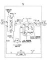
図1は、新規の一態様による、単一の集積回路上に統合されたアナログ位相ロックループ(PLL)100の図である。PLL100は、導線102上で基準クロック信号FREF101を受け、導線104上で出力信号VCO_OUT103を出力する。出力信号VCO_OUTの周波数は、入力信号FREF101の周波数の所望の整数倍である。フィードバック分割器105が除算するのに使う整数を変えることによって、出力信号VCO_OUT103の周波数は、約1GHz〜約3GHzの範囲で変更可能である。PLL100は、位相周波数検出器(PFD)106、電荷ポンプ(CP)107、ループフィルタ108、電圧制御発振器(VCO)109、フィードバック分割器105、およびキャパシタ漏れ補償回路110を含む。PFD106は、フィードバック信号FDIV111のエッジの時間を、入力信号FREF101のエッジの時間と比較し、制御信号UP、UPB、DNおよびDNBを出力する。制御信号は、2つのエッジの間の相対時間差を示す。
FIG. 1 is a diagram of an analog phase locked loop (PLL) 100 integrated on a single integrated circuit, according to a novel aspect.
たとえば、フィードバック信号FDIV111のエッジが入力信号FREF101のエッジに続くことをPFD106が検出した場合、これらのエッジの間の時間に、制御信号UP、UPB、DNおよびDNBがアサートされる。FDIV111およびFREF101のエッジの間の時間差が長いほど、制御信号UP、UPB、DNおよびDNBがアサートされる時間が長くなる。電荷ポンプ107は、アサートされた制御信号を、対応する正の電流パルスICP112に変換し、このパルスは、電荷ポンプ出力ノード113上へ出力される。
For example, if the
たとえば、フィードバック信号FDIV111のエッジが、入力信号FREF101のエッジに先立つことを、PFD106が検出した場合、電荷ポンプ107が電流パルスICP112を電荷ポンプ出力ノード113から引き込むように制御されるように、FDIV111およびFREF101のエッジの間の時間に、制御信号UP、UPB、DNおよびDNBが生成される。ノード113から電流パルスを引き込むのは、ノード113上へ負の電流パルスを供給するのと同じことである。
For example, if the
これらの正の電流パルスと負の電流パルスは、比較的ゆっくり変化する制御信号VTUNE115が、ループフィルタの出力におけるノード116上へ生成されるように、ループフィルタ108のキャパシタ114(ならびにキャパシタ130および131)上で統合される。VTUNE115は、VCO109の制御入力リード117上へ供給される。VCO109は、出力リード118上へ振動出力信号VCO_OUT103を生成する。信号VCO_OUTの周波数は、VTUNE115のレベルによって決まる。VTUNEのレベルを上げると、VCOは、信号VCO_OUT103の周波数を増大させ、VTUNEのレベルを下げると、VCOは、信号VCO_OUT103の周波数を減少させる。信号VCO_OUT103は、フィードバック分割器105の入力リード119に供給される。フィードバック分割器105は、VCO_OUT信号を整数の除数で周波数分割し、その結果得られた、より低い周波数信号FDIV111を、その出力リード120から出力する。フィードバック信号FDIV111は、導線121を介して、PFD106の第2の入力リード122に供給される。PFD106は、PFD106の第1の入力リード123上で、入力基準信号FREF101を受ける。PLL100がロック中のとき、FDIV信号111の周波数および位相は、FREF信号101の周波数および位相にロックされる。
These positive and negative current pulses cause the capacitor 114 (and
ループフィルタ108は、電荷ポンプ107から、電荷ポンプ出力ノード113を介して正および負の電流パルスICP112を受け、得られたフィルタリング済み信号VTUNE115をノード116上に出力する。ループフィルタ108は、大型キャパシタ114に加え、2つの抵抗器128および129、ならびに2つのより小型なキャパシタ130および131を含む。一例では、PLLは、100kHz未満のループ帯域幅を有し、キャパシタ114、130および131は、それぞれ、500pF、20pFおよび10pFの静電容量を有し、抵抗器128および129は、それぞれ、40kオームおよび20kオームの抵抗を有する。抵抗器128は、図示のように、電荷ポンプ出力ノード113と大型キャパシタ114との間に結合される。抵抗器128は、電荷ポンプ出力ノード113に直接接続された第1のリードを有し、大型キャパシタ114に直接接続された第2のリードを有する。
本例において、大型キャパシタ114は、薄膜酸化物を有するオンチップ金属酸化膜半導体キャパシタ(MOSCAP)として実現される。静電容量は、MOSCAPのゲート金属と、基礎をなす半導体材料中の空間電荷空乏領域との間で形成される。キャパシタ130および131は、一方、キャパシタ114よりもはるかに小さい静電容量を有するキャパシタである。これらのキャパシタ130および131は、MOSCAPキャパシタとしても実現されるが、静電容量が比較的小さいので、集積回路面積を犠牲にしすぎることなく、厚膜酸化物MOSCAPとして実現される。本例において、所与の静電容量の薄膜酸化物MOSCAPは、同じ静電容量の厚膜酸化物MOSCAPが消費する集積回路面積の約半分を消費するが、薄膜酸化物MOSCAPキャパシタは、厚膜酸化物MOSCAPキャパシタと比較して、より高い電流漏れを呈する。キャパシタ114両端間の電圧V1は、PLL制御ループが、FREF信号101の位相にロックされているFDIV信号111の位相を保つように動作すると、増大および減少する。ただし、キャパシタ114両端間の所与の電圧に対して、キャパシタ114は、その第1のプレート133からその第2のプレート134に、漏れ電流132を漏らす。キャパシタ114両端間の電圧V1が変わると、この漏れ電流132は変わるが、キャパシタ114は常に漏れがある。漏れ補償がないと、キャパシタ114を通る電流の一定の漏れは、VTUNEを不適切に低くすることによって、PLL動作に悪影響を与え得る。しかし、PLL制御ループが動作すると、制御ループは、漏れの補償を試み、この補償自体が、増大するVTUNE電圧として現れる。VTUNEは、所望通り固定値であるよりもむしろ、適切なVTUNE値の周囲で、増大および減少するのがわかる。その結果生じる、VTUNEの変動(リップルと呼ばれる)により、対応する望ましくない追加周波数成分がPLL出力信号に生じる。キャパシタ漏れ補償回路110はしたがって、ノード136からキャパシタ114を通ってグラウンドに漏れる漏れ電流132を補償するために、ノード136上へ補償電流135を供給するように動作する。キャパシタ漏れ補償回路110は、後でさらに詳しく説明するように、電荷ポンプ107内の「電荷ポンプ出力電圧レプリカノード」(CPOVRN)上に存在する検知電圧137を検知することによって、キャパシタ114両端間の電圧を間接的に検出する。CPOVRNからの検知電圧137は、キャパシタ114両端間の電圧V1を示す。キャパシタ漏れ補償回路110は、その入力138上への検知電圧137を受け、検知電圧137を使って、出力139を介してノード136上へ供給される補償電流135の大きさを制御する。
In this example, the
図2は、電荷ポンプ107、ループフィルタ108およびキャパシタ漏れ補償回路110をさらに詳しく示す図である。電荷ポンプ107は、電流制御部分141および出力部分142を含む。電荷ポンプ107は、PFD106から入力リード124〜127を介して、それぞれ、制御信号UP、UPB、DNおよびDNBを受ける。電荷ポンプ107は、電荷ポンプ出力リード140から電流パルスを出力する。
FIG. 2 is a diagram showing the
PFD106が制御信号をアサート中でないとき、信号UPはデジタル論理低にあり、信号UPBはデジタル論理高にあり、信号DNはデジタル論理低にあり、信号DNBはデジタル論理高にある。Pチャネル電界効果トランジスタ143がしたがって、オンになり、Nチャネル電界効果トランジスタ144がオンになる。Pチャネルトランジスタ145はオフになる。Nチャネルトランジスタ146はオフになる。接地導線148から、トランジスタ146を通って電荷ポンプ出力ノード113に向かうどの電流経路もそうであるように、VDD電源電圧導線147から、トランジスタ145を通って電荷ポンプ出力ノード113に向かうどの電流経路も遮断される。電荷ポンプ107は、そのようなとき、ノード113上で静電容量を充電も放電もしない。
When
PFD106が正電流パルスICPを生成するために制御信号をアサート中であるとき、信号UPはデジタル論理高にあり、信号UPBはデジタル論理低にあり、信号DNはデジタル論理低にあり、信号DNBはデジタル論理高にある。Pチャネルトランジスタ145はしたがって、オンになり、Nチャネルトランジスタ146はオフになる。トランジスタ143はオフになる。したがって、供給導線147から、トランジスタ145を通り、トランジスタ149を通ってノード113に向かう電流経路が確立される。Pチャネルトランジスタ149がオンであるとともに導電性をもつ程度により、正電流パルスICPの大きさが決まる。Pチャネルトランジスタ149が導電性をもつ程度は、トランジスタ149のゲート、ソースおよびドレイン上の電圧によって決まり、これらの電圧は、電流制御部分141によって制御される。正電流パルスICPの持続時間は、制御信号UP、UPB、DNおよびDNBのアサートを起こした、信号FDIV111と信号FREF101のエッジの間の時間差によって決まる。
When the
PFD106が負電流パルスICPを生成するために制御信号をアサート中であるとき、信号DNはデジタル論理高にあり、信号DNBはデジタル論理低にあり、信号UPはデジタル論理低にあり、信号UPBはデジタル論理高にある。Nチャネルトランジスタ146はオンになり、Pチャネルトランジスタ145はオフになる。トランジスタ144はオフになる。したがって、ノード113から、トランジスタ150を通り、トランジスタ146を通って接地導線148に向かう電流経路が確立される。Nチャネルトランジスタ150が導電性をもつ程度により、負電流パルスICPの大きさが決まる。Nチャネルトランジスタ150が導電性をもつ程度は、トランジスタ150のゲート、ソースおよびドレイン上の電圧によって決まり、これらの電圧は、電流制御部分141によって決まる。負電流パルスICPの持続時間は、制御信号UP、UPB、DNおよびDNBのアサートを起こした、信号FDIV111と信号FREF101のエッジの間の時間差によって決まる。
When the
電荷ポンプ107の電流制御部分141は、トランジスタ151〜154および演算増幅器156を含む。トランジスタ151〜154は、VDD導線147から、「電荷ポンプ出力電圧レプリカノード」(CPOVRN)159を通って、接地導線148への電流経路を形成する。トランジスタ151〜154は、Pチャネルトランジスタ151が常にオンであるように接続され、Nチャネルトランジスタ154が常にオンであるように接続されることを除いて、出力部分142のトランジスタ145、149、150および146に対応する。電流制御部分141のトランジスタ153のゲートおよび出力部分142のNチャネルトランジスタ150のゲートには、バイアス電圧VBIASが供給される。大きくは、このVBIAS電圧により、トランジスタ150の導電性が決まり、したがって、電荷ポンプによって生成される負電流パルスの大きさが設定される。
The
演算増幅器156の高インピーダンス入力リード158への、またはリード158からの、ごくわずかな電流フローがある。Pチャネルトランジスタ152を通るソースドレイン電流フローはしたがって、Nチャネルトランジスタ153を流れる電流と同じである。トランジスタ145がオンである場合、この同じ量の電流がPチャネルトランジスタ149を通って流れるように、また、トランジスタ146がオンである場合、この同じ量の電流がNチャネルトランジスタ150を流れるように、この電流を、出力部分142に対して複製することが所望される。Pチャネルトランジスタ149のソース、ゲートおよびドレイン電圧が、Pチャネルトランジスタ152の対応するソース、ゲートおよびドレイン電圧と同じである場合、この電流複製が起こる。トランジスタ152および149のゲートはしたがって、それらのゲート電圧が同じになるように共に、演算増幅器156の出力リード155に結合される。完全にオンのPチャネルトランジスタ151に渡る電圧降下は、トランジスタ145がオンであるように制御されるときの、完全にオンのPチャネルトランジスタ145に渡る電圧降下と同様に、非常に小さい。したがって、トランジスタ152および149のソース電圧は、(電源電圧VDDに近い電圧において)本質的に同じである。演算増幅器156は、トランジスタ149上のドレイン電圧を、トランジスタ152上のドレイン電圧と同じに維持するように動作する。演算増幅器156が負のフィードバックループ内で動作中であるとき、その反転入力リード157およびその非反転入力リード158上の電圧はほぼ同一である。トランジスタ149のソース、ゲートおよびドレイン電圧は、トランジスタ152のソース、ゲートおよびドレイン電圧と同じなので、2つのトランジスタ152および149は同一にバイアスされ、電流制御部分141を流れる電流は、出力部分142中のトランジスタ149を流れるように複製される。同じやり方で、Nチャネルトランジスタ150のゲート、ソースおよびドレイン電圧は、Nチャネルトランジスタ153の対応するゲート、ソースおよびドレイン電圧と同じである。したがって、トランジスタ146がオンであるとき、電荷ポンプの出力部分142のトランジスタ150を通る電流フローは、電荷ポンプの電流制御部分141のトランジスタ153を通る電流フローと同じである。電荷ポンプの電流制御部分141はしたがって、正電流パルスICPの大きさが、負電流パルスICPの大きさと同じになるように、トランジスタ149および150を制御する。VBIASの増大により、ICP112の正および負のパルス両方の大きさが増大する。VBIASの減少により、ICP112の正および負のパルス両方の大きさが減少する。本例におけるVBIASは固定電圧であるが、他の例では可変であってよい。
There is negligible current flow to or from the high
ループフィルタ108は、2つの入力160および161ならびに1つの出力162を有すると見なすことができる。ループフィルタ108は、図示のように、2つの受動RCローパスフィルタ177および178を含む。抵抗器128およびキャパシタ130が、第1の受動RCローパスフィルタ177を形成する。抵抗器129およびキャパシタ131が、第2の受動RCローパスフィルタ178を形成する。2つの受動RCローパスフィルタ177および178は、ノード136と、VCO109の入力リード117との間で直列に共に連結される。キャパシタ漏れ補償回路110によってノード136上へ生成される雑音は、VCO109の制御入力リード117に達するために、これらの2つの受動RCローパスフィルタ177と178の両方を通過しなければならない。
The
キャパシタ漏れ補償回路110は、電荷ポンプ107内のCPOVRNノード159から検知電圧137を受けるための入力138を有する。キャパシタ漏れ補償回路110は、ループフィルタのキャパシタ114のプレート133上への補償電流135の供給元である出力139を有する。キャパシタ漏れ補償回路110は、図示のように相互接続された、演算増幅器163、2つのPチャネル電界効果トランジスタ164および165、およびレプリカキャパシタ166を含む。演算増幅器163の出力リード167は、トランジスタ164のゲート168に、およびトランジスタ165のゲート169に結合される。トランジスタ164のソース170およびトランジスタ165のソース171は両方とも、VDD供給導線147に結合される。トランジスタ164のドレイン172は、レプリカキャパシタ166のプレート173に、および演算増幅器163の非反転入力リード174に結合され、そうすることによって、演算増幅器163の反転入力リード175上の電圧が、レプリカキャパシタ166両端間で維持される。レプリカキャパシタ166両端間に加えられる電圧は、電圧V2で示される。トランジスタ164および165は、カレントミラーを形成する。トランジスタ165を流れる電流は、トランジスタ164を流れる電流のN倍の大きさになるようにミラーリングされる。Nは、約20〜約30の範囲であり、本例では21である。レプリカキャパシタ166は、ループフィルタの漏れキャパシタ114のN分の1の大きさなので、両方のキャパシタ両端間に同じ電圧が存在すると仮定すると、および両方のキャパシタが同じ薄膜酸化物MOSCAP構造を有すると仮定すると、レプリカキャパシタ166は、キャパシタ114のN分の1の電流を漏らす。レプリカキャパシタ166を通って漏れる電流は、カレントミラーのトランジスタ164を通して伝導される。カレントミラーの動作により、このレプリカキャパシタ漏れ電流のN倍が、補償電流135の形で、トランジスタ165のドレイン176からノード136に流される。
Capacitor
図3は、電荷ポンプ107、キャパシタ漏れ補償回路110、およびループフィルタ108の一部の別の図である。図3の線図は、電流ICP112の正電流パルス179を示す。正電流パルス179は、矢印180で示される電流経路を流れる。この電流パルス179の大きさ181は、上で説明したように、電荷ポンプの電流制御部分141によって決まる。この線図は、電流ICP112の負電流パルス182も示す。矢印183は、このパルスの経路が接地導線148からノード113に延びることを示すが、このパルスは、負の電流パルスであると理解される。実際の電流フローの方向は、ノード113から接地導線148へ向かう。負電流パルス182の大きさ186は、上で説明したように、電荷ポンプの電流制御部分141によって決まる。
FIG. 3 is another diagram of a portion of
キャパシタ漏れ補償回路110は、キャパシタ114両端間の電圧V1を、次のように間接的に検知する。定常状態動作中は、抵抗器128両端間のごくわずかな電流フローしかない。電荷ポンプ出力ノード113上の電圧はしたがって、ノード136上の電圧に非常に近い。演算増幅器156が定常状態動作で動作中のとき、演算増幅器156の2つの入力リード157および158上の電圧の間には、ごくわずかな電圧差しかない。演算増幅器は、その非反転入力リード158上の電圧を、その反転入力リード157上に存在する同じ電圧に維持するように動作する。ノード159はしたがって、このノード上の電圧が、電荷ポンプ出力ノード113上の電圧のレプリカであるという点で、「電荷ポンプ出力電圧レプリカノード」(CPOVRN)159と呼ばれる。新規の一態様によると、CPOVRN159は、キャパシタ漏れ補償回路110の演算増幅器163の反転入力リード175に直接接続される。キャパシタ漏れ補償回路110は、CPOVRN159上の検知電圧137を検知することによって、キャパシタ114両端間の電圧V1を間接的に検知する。キャパシタ漏れ補償回路110の演算増幅器163の検知側入力リードは、VCO109の制御入力リード117に直接接続されるのではなく、漏れキャパシタ114におけるノード136に直接接続されるのでもなく、ループフィルタ内の他のどのノードに直接接続されるのでもなく、ノード113における電荷ポンプの出力に直接接続されるのでもない。電荷ポンプ107の電流制御部分141内のCPOVRN159上に存在する電圧を検知することによる、漏れキャパシタ114両端間の電圧V1の間接検知には、米国特許第6,956,417号および第6,963,232号の従来技術の回路に勝る利点がある。
The capacitor
図4は、雑音が、キャパシタ漏れ補償回路110内の雑音源から伝わるとともに、VCO109の制御入力リード117に伝わる際にとり得る2つの可能な経路を示す図である。雑音は、たとえば、演算増幅器163の入力段によって生成され得る。この雑音は、キャパシタ漏れ補償回路110によって出力される補償電流信号135中に出現し得る。加えて、導線147からの電源雑音は、キャパシタ漏れ補償回路110によって出力される補償電流信号135中にも存在し得る。矢印184は、そのような雑音が、VCO109の制御入力リード117に達するのにとらなければならない経路を示す。雑音は、受動ローパスフィルタ177と178の両方を通らなければならない。フィルタ177および178は有利には、そのような雑音を減衰する。一方、米国特許第6,956,417号の回路では、漏れ補償回路のカレントミラーのドレインは、VCOの入力に直接接続される。介入フィルタによる、雑音の減衰はない。雑音は、VCOの入力上へ直接注入される。
FIG. 4 is a diagram illustrating two possible paths that can be taken when noise travels from a noise source in capacitor
キャパシタ漏れ補償回路110からの雑音がVCO109の制御入力リード117に達し得るための第2の経路もある。演算増幅器163の入力段において生成される雑音は、検知演算増幅器の反転入力リード175から出てよく、矢印185によって示される経路に沿って、VCO109の制御入力リード117に進んでよい。演算増幅器156と第2の受動ローパスフィルタ178の両方が、この経路185中にある。演算増幅器156および第2のローパスフィルタ178を含む、この経路185中の回路構成は、CPOVRNノード159上の雑音がVCO入力に達するのを防止するのを助けるために、望ましい減衰手段を提供する。米国特許第6,963,232号の従来技術のように、検知演算増幅器の反転入力リードがVCOの入力に直接接続されるのではなく、図4の回路中の検知演算増幅器163の反転入力リード175は、CPOVRNノード159に接続される。
There is also a second path for noise from the capacitor
図3の回路は、受動ループフィルタを使うという点で、米国特許第6,956,417号の回路と同様であるが、その補償回路(その入力経路と出力経路の両方)が、その雑音がVCO入力に結合される前にフィルタリングされるという点では異なる。図3の回路は、補償回路の出力がフィルタリングされるという点で、米国特許第6,963,232号の回路と同様であるが、その出力がより効率的にフィルタリングされ(米国特許第6,956,417号の回路では、補償回路の出力が明らかなローパスフィルタリングを経ない)、その入力雑音がフィルタリングされ、受動フィルタを伴う(米国特許第6,963,232号の回路は、能動フィルタを有する)という点では異なる。 The circuit of Figure 3 is similar to the circuit of US Pat. No. 6,956,417 in that it uses a passive loop filter, but its compensation circuit (both its input and output paths) has its noise coupled to the VCO input. It is different in that it is filtered before being done. The circuit of FIG. 3 is similar to the circuit of US Pat.No. 6,963,232 in that the output of the compensation circuit is filtered, but its output is filtered more efficiently (in the circuit of US Pat. No. 6,956,417, The difference is that the output of the compensation circuit does not go through obvious low-pass filtering), and its input noise is filtered and accompanied by a passive filter (the circuit of US Pat. No. 6,963,232 has an active filter).
図5は、キャパシタ114が、いかなるキャパシタ漏れ補償回路ももたない厚膜酸化物MOSCAPとして実現されるとき、およびキャパシタ114が、図2のキャパシタ漏れ補償回路110をもつ薄膜酸化物MOSCAPとして実現されるときに占める集積回路面積の量を比較する図である。線200は、キャパシタ114が厚膜酸化物MOSCAPとして実現されるとき、およびキャパシタ漏れ補償回路が設けられない場合に消費される集積回路面積の量を示す。線201は、キャパシタ114が薄膜酸化物MOSCAPとして実現されるとき、および図2のキャパシタ漏れ補償回路110が設けられる場合に消費される集積回路総面積を示し、ここでN=21であり、キャパシタ114の静電容量は500pFである。この状況において、キャパシタ漏れ補償回路110は、約70ミクロン×70ミクロンの集積回路面積を占める。キャパシタ漏れ補償回路110の電流消費は、50マイクロアンペアである。抵抗器128を通る平均漏れ電流は、約0.03マイクロアンペアである。位相マージンは、89度(PVTを上回る60度〜127度)である。低周波数ループ利得は、25dB(PVTを上回る2dB〜53dB)である。2dBループ利得値は、漏れが最も小さい、遅いプロセスコーナー向けであり、53dBループ利得値は、漏れが比較的大きい、高速プロセスコーナー向けである。漏れ訂正誤差率が比較的大きいときに小さいループ利得を有することは、実際の漏れ電流値が小さいので、問題ない。キャパシタ漏れ補償回路110が不能にされた場合、抵抗器128を通る平均電流フローによって示される漏れ電流132は約4.5マイクロアンペアになる。
FIG. 5 shows that when
線202は、1)いかなるキャパシタ漏れ補償回路ももたないキャパシタ114に厚膜酸化物MOSCAPを使う場合と、2)図2のキャパシタ漏れ補償回路をもつキャパシタ114に薄膜酸化物MOSCAPを使う場合との間の、集積回路面積の差を示す。図5の例において、検討される各MOSCAPは実際に、MOSCAP構造のすぐ上に配置された側壁静電容量RTMOMキャパシタ構造を含み、追加RTMOMキャパシタ構造によって与えられる側壁静電容量は、金属層1〜4を伴う、間隔が密な金属列の間にある。
図6は、厚膜酸化物MOSCAPを使用し、キャパシタ漏れ補償回路を使用しないときと比較して、図2のキャパシタ漏れ補償回路110を使う際に実現される面積節約率を示す図である。線203は、キャパシタ114の値が小さい場合は、節約される面積率が小さいことを示す。というのは、キャパシタ114のサイズにかかわらず、比較的固定された量の集積回路面積が、キャパシタ漏れ補償回路110を実現するのに必要とされるからである。
FIG. 6 is a diagram illustrating the area saving ratio realized when using the capacitor
図7は、VTUNEの周波数成分を示す図であり、ここでPLLは定常状態にあり、FREF信号101は20MHzであり、PLLは、キャパシタ114用に厚膜酸化物MOSCAPを使う実装形態であり、キャパシタ漏れ補償回路はない。理想的には、VTUNEは、非ゼロ周波数成分をもたないDC信号であるが、現実には、キャパシタ漏れおよび他の要因の結果として、VTUNE信号中のリップルにより、比較的高い周波数成分がある。図7は、20MHzでの信号VTUNEのボルトピーク(リップルのピークツーピーク電圧の半分)が、マイナス117dBVpという最悪のケースであることを示す。
FIG. 7 is a diagram showing the frequency components of VTUNE, where the PLL is in a steady state, the
図8は、図1のPLLが定常状態で動作中のときのVTUNEの周波数成分を示す図であり、FREF信号101は20MHzである。20MHzでの信号VTUNEのボルトピーク(リップルのピークツーピーク電圧の半分)が、マイナス112dBVpという最悪のケースである。したがって、図8は、図1のPLL中のVTUNEには、図7に示されるように、キャパシタ114用に厚膜酸化物MOSCAPを使うケースよりもわずかに多くのリップルがあるが、リップルの増大量はわずかであることを示す。
FIG. 8 is a diagram showing the frequency components of VTUNE when the PLL of FIG. 1 is operating in a steady state, and the
図9は、PLLがキャパシタ114用に厚膜酸化物MOSCAPを使い、PLLがキャパシタ漏れ補償回路をもたない、PLLのVCO出力信号中の閉ループ位相雑音を示す図である。
FIG. 9 is a diagram illustrating closed loop phase noise in the VCO output signal of the PLL where the PLL uses a thick oxide MOSCAP for the
図10は、PLL100がキャパシタ114用に薄膜酸化物MOSCAPを使い、PLL100が図2のキャパシタ漏れ補償回路110を伴う、図1のPLLのVCO出力信号VCO_OUT103中の閉ループ位相雑音を示す図である。図10に示される位相雑音は、図9に示される位相雑音よりもわずかに悪いだけである。図9および図10のグラフに提示される、比較のためのデータは、ノイズのないVCOを用いてPLL回路をシミュレートすることによって取得された。図9と図10の両方に示される少量の位相雑音は、現実のPLLにおいて、VCOによって生成される雑音の方が上回るほど小さい。したがって、図2のキャパシタ漏れ補償回路110をPLLに追加しても、全体的なPLL位相雑音は増大しない。
FIG. 10 is a diagram illustrating closed loop phase noise in the VCO output signal VCO_OUT103 of the PLL of FIG. 1, where the
図11は、新規な一態様による方法300のフローチャートである。正電流パルスおよび負電流パルスが、電荷ポンプから、電荷ポンプ出力ノードを介してループフィルタに供給される(ステップ301)。一例では、正電流パルスおよび負電流パルスは共に、図2でICPと示される電流信号112である。電流パルスは、ループフィルタを用いてフィルタリングされ(ステップ302)、ループフィルタは漏れキャパシタを含む。一例では、ループフィルタは図2のループフィルタ108であり、漏れキャパシタは図2のキャパシタ114である。電荷ポンプ内の「電荷ポンプ出力電圧レプリカノード」(CPOVRN)上の検知電圧が検知される(ステップ303)。一例では、検知電圧は図2の検知電圧137であり、CPOVRNは図2のノード159である。検知電圧は、図2のキャパシタ漏れ補償回路110の演算増幅器163によって検知される。電荷ポンプ内の回路構成は、CPOVRN上の検知電圧を、電荷ポンプ出力ノード上の電圧と同じに維持するように機能する。一例では、CPOVRN上の電圧を、電荷ポンプ出力ノード上の電圧と同じに維持する回路構成は、演算増幅器156である。検知電圧が、レプリカキャパシタ両端間に加えられる(ステップ304)。レプリカキャパシタ漏れ電流は、レプリカキャパシタを通って漏れる。一例では、レプリカキャパシタは図2のキャパシタ166である。レプリカキャパシタ漏れ電流はミラーリングされ(ステップ305)、そうすることによって、補償電流を生成する。一例では、ミラーリングは、トランジスタ164および165を伴う図2のカレントミラーによって実施される。補償電流は、漏れキャパシタ上へ供給される(ステップ306)。一例では、補償電流は図2の電流135である。この電流135は、図2のノード136上へ供給される。一例では、ステップ303〜306は、図2のキャパシタ漏れ補償回路110によって実施される。図11の方法のステップは、フローチャートにあるように示されているが、これらのステップの動作は実際にはすべて、同時に実施されている。
FIG. 11 is a flowchart of a
教授の目的で、いくつかの特定の実施形態について上記で説明したが、本特許文献の教示は一般的な適用性を有し、上記で説明した特定の実施形態に限定されない。したがって、以下に記載する特許請求の範囲から逸脱することなく、説明した特定の実施形態の様々な特徴の様々な変更、適応、組合せを実践することができる。 For teaching purposes, several specific embodiments have been described above, but the teachings of this patent document have general applicability and are not limited to the specific embodiments described above. Accordingly, various modifications, adaptations, and combinations of the various features of the specific embodiments described can be practiced without departing from the scope of the claims that are set forth below.
100 アナログ位相ロックループ(PLL)
101 基準クロック信号、入力信号
102 導線
103 出力信号、信号
104 導線
105 フィードバック分割器
106 位相周波数検出器(PFD)
107 電荷ポンプ(CP)
108 ループフィルタ
109 電圧制御発振器(VCO)
110 キャパシタ漏れ補償回路
111 フィードバック信号
112 正の電流パルス、電流パルス、電流
113 電荷ポンプ出力ノード、ノード
114 キャパシタ
115 制御信号、信号
116 ノード
117 制御入力リード、入力リード
118 出力リード
119 入力リード
120 出力リード
121 導線
122 入力リード
123 入力リード
128 抵抗器
129 抵抗器
130 キャパシタ
131 キャパシタ
132 漏れ電流
133 プレート
134 プレート
135 補償電流、補償電流信号
136 ノード
137 検知電圧
138 入力
139 出力
140 電荷ポンプ出力リード
141 電流制御部分
142 出力部分
143 Pチャネル電界効果トランジスタ、トランジスタ
144 Nチャネル電界効果トランジスタ、トランジスタ
145 Pチャネルトランジスタ、トランジスタ
146 Nチャネルトランジスタ、トランジスタ
147 VDD電源電圧導線、供給導線、VDD導線、VDD供給導線、導線
148 接地導線
149 トランジスタ、Pチャネルトランジスタ
150 トランジスタ、Nチャネルトランジスタ
151 トランジスタ、Pチャネルトランジスタ
152 トランジスタ、Pチャネルトランジスタ
153 トランジスタ、Nチャネルトランジスタ
154 トランジスタ
155 出力リード
156 演算増幅器
157 入力リード
158 入力リード
159 電荷ポンプ出力電圧レプリカノード(CPOVRN)、ノード
160 入力
161 入力
162 出力
163 演算増幅器
164 Pチャネル電界効果トランジスタ、トランジスタ
165 Pチャネル電界効果トランジスタ、トランジスタ
166 レプリカキャパシタ
167 出力リード
168 ゲート
169 ゲート
170 ソース
171 ソース
173 プレート
174 入力リード
175 入力リード
176 ドレイン
177 受動RCローパスフィルタ、受動ローパスフィルタ、フィルタ
178 受動RCローパスフィルタ、受動ローパスフィルタ、フィルタ
179 正電流パルス、電流パルス
182 負電流パルス
100 analog phase-locked loop (PLL)
101 Reference clock signal, input signal
102 conductor
103 Output signal, signal
104 conductor
105 Feedback divider
106 Phase frequency detector (PFD)
107 Charge pump (CP)
108 Loop filter
109 Voltage controlled oscillator (VCO)
110 Capacitor leakage compensation circuit
111 Feedback signal
112 positive current pulse, current pulse, current
113 Charge pump output node, node
114 capacitors
115 Control signals, signals
116 nodes
117 Control input lead, input lead
118 Output lead
119 Input lead
120 output leads
121 conductor
122 Input lead
123 Input lead
128 resistors
129 resistor
130 capacitors
131 capacitors
132 Leakage current
133 plates
134 plates
135 Compensation current, compensation current signal
136 nodes
137 Detection voltage
138 inputs
139 output
140 Charge pump output lead
141 Current control part
142 Output part
143 p-channel field effect transistors, transistors
144 N-channel field effect transistors, transistors
145 P-channel transistors, transistors
146 N-channel transistors, transistors
147 VDD power supply voltage lead, supply lead, VDD lead, VDD supply lead, lead
148 Grounding conductor
149 Transistors, P-channel transistors
150 transistors, N-channel transistors
151 transistors, p-channel transistors
152 transistors, P-channel transistors
153 transistors, N-channel transistors
154 transistors
155 Output lead
156 operational amplifier
157 Input lead
158 Input lead
159 Charge pump output voltage replica node (CPOVRN), node
160 inputs
161 inputs
162 outputs
163 operational amplifier
164 P-channel field effect transistors, transistors
165 P-channel field effect transistor, transistor
166 Replica capacitor
167 Output lead
168 Gate
169 Gate
170 sources
171 source
173 plates
174 Input lead
175 input leads
176 drain
177 Passive RC low pass filter, passive low pass filter, filter
178 Passive RC low pass filter, passive low pass filter, filter
179 Positive current pulse, current pulse
182 Negative current pulse
Claims (15)
電荷ポンプ出力ノードおよび電荷ポンプ出力電圧レプリカノード(CPOVRN)を備える電荷ポンプであって、前記電荷ポンプ出力ノードが、前記ループフィルタに結合されている、電荷ポンプと、
前記CPOVRN上に存在する検知電圧を検知し、この検知電圧をレプリカキャパシタ両端間に加えるキャパシタ漏れ補償回路であって、前記キャパシタのプレート上へ補償電流を供給し、前記レプリカキャパシタ両端間の前記検知電圧が、前記キャパシタ両端間の電圧とほぼ同一であるキャパシタ漏れ補償回路とを備える回路。 A loop filter comprising a capacitor;
A charge pump comprising a charge pump output node and a charge pump output voltage replica node (CPOVRN), wherein the charge pump output node is coupled to the loop filter;
A capacitor leakage compensation circuit for detecting a detection voltage existing on the CPOVRN and applying the detection voltage across the replica capacitor, supplying a compensation current to the plate of the capacitor, and detecting the detection across the replica capacitor; A circuit comprising: a capacitor leakage compensation circuit whose voltage is substantially the same as the voltage across the capacitor.
ゲート、ソース、およびドレインを有する第1のトランジスタであって、前記ドレインが前記レプリカキャパシタに結合されている、第1のトランジスタと、
ゲート、ソース、およびドレインを有する第2のトランジスタであって、前記ドレインが、前記ループフィルタの前記キャパシタのプレートに結合されている、第2のトランジスタと、
非反転入力リード、反転入力リード、および出力リードを有する演算増幅器であって、前記演算増幅器の前記出力リードが、前記第1のトランジスタの前記ゲートに結合されているとともに前記第2のトランジスタの前記ゲートに結合され、前記非反転入力リードが前記レプリカキャパシタに結合され、前記反転入力リードが、前記電荷ポンプの前記電流制御部分内の前記CPOVRNに結合されている、演算増幅器とをさらに備える、請求項2に記載の回路。 The capacitor leakage compensation circuit is
A first transistor having a gate, a source, and a drain, wherein the drain is coupled to the replica capacitor;
A second transistor having a gate, a source, and a drain, wherein the drain is coupled to a plate of the capacitor of the loop filter;
An operational amplifier having a non-inverting input lead, an inverting input lead, and an output lead, wherein the output lead of the operational amplifier is coupled to the gate of the first transistor and the second transistor An operational amplifier coupled to a gate, the non-inverting input lead coupled to the replica capacitor, and the inverting input lead coupled to the CPOVRN in the current control portion of the charge pump. The circuit according to Item 2.
前記電荷ポンプ出力ノードと前記キャパシタのプレートとの間に結合された抵抗器、および前記電荷ポンプ出力ノードと電圧制御発振器(VCO)の入力リードとの間に結合された受動ローパスフィルタ、のうちの少なくとも1つをさらに備える、請求項2に記載の回路。 The loop filter is
A resistor coupled between the charge pump output node and the plate of the capacitor; and a passive low pass filter coupled between the charge pump output node and an input lead of a voltage controlled oscillator (VCO). The circuit of claim 2 further comprising at least one.
(b)前記ループフィルタを使って前記正電流パルスおよび前記負電流パルスをフィルタリングするステップであって、前記ループフィルタがキャパシタを備えるステップと、
(c)前記電荷ポンプ内の電荷ポンプ出力電圧レプリカノード(CPOVRN)上に存在する検知電圧を検知するステップと、
(d)レプリカキャパシタを通ってレプリカ電流が漏れるように、前記検知電圧を前記レプリカキャパシタ両端間に加えるステップであって、前記レプリカキャパシタが、前記ループフィルタの前記キャパシタのレプリカであるが、前記ループフィルタの前記キャパシタよりも小さい静電容量を有する、ステップと、
(e)前記レプリカ電流をミラーリングし、そうすることによって補償電流を生成するステップと、
(f)前記補償電流を、前記ループフィルタの前記キャパシタのプレート上へ供給するステップとを含み、前記検知電圧が、前記キャパシタ両端間の電圧とほぼ同一である、方法。 (a) supplying a positive current pulse and a negative current pulse from the charge pump to the loop filter via the charge pump output node;
(b) filtering the positive current pulse and the negative current pulse using the loop filter, the loop filter comprising a capacitor;
(c) detecting a detection voltage present on a charge pump output voltage replica node (CPOVRN) in the charge pump;
(d) applying the sensed voltage across the replica capacitor so that a replica current leaks through the replica capacitor, the replica capacitor being a replica of the capacitor of the loop filter, wherein the loop Having a smaller capacitance than the capacitor of the filter;
(e) mirroring the replica current and thereby generating a compensation current;
(f) is the compensation current, see containing and supplying to plates of the capacitor of the loop filter, the detection voltage is substantially the same as the voltage between the capacitor ends, methods.
(g)前記出力部分から、前記電荷ポンプ出力ノードを介して前記ループフィルタに正電流パルスおよび負電流パルスを供給するステップと、
(h)前記正電流パルスが前記負電流パルスと同じ大きさになるように、前記出力部分を制御するステップであって、前記電流制御部分が、少なくとも部分的には、前記CPOVRN上の前記検知電圧を、前記電荷ポンプ出力ノード上に存在する電圧とほぼ同一であるように維持することによって、制御する前記ステップを実施する、ステップとをさらに含む、請求項10に記載の方法。 The charge pump includes a current control portion and an output portion, the method comprising:
(g) supplying a positive current pulse and a negative current pulse from the output portion to the loop filter via the charge pump output node;
(h) controlling the output portion such that the positive current pulse is the same magnitude as the negative current pulse, wherein the current control portion is at least partially the detection on the CPOVRN. 11. The method of claim 10, further comprising the step of performing the step of controlling by maintaining a voltage to be approximately the same as the voltage present on the charge pump output node.
Applications Claiming Priority (3)
| Application Number | Priority Date | Filing Date | Title |
|---|---|---|---|
| US13/409,348 | 2012-03-01 | ||
| US13/409,348 US9166607B2 (en) | 2012-03-01 | 2012-03-01 | Capacitor leakage compensation for PLL loop filter capacitor |
| PCT/US2013/028711 WO2013131027A1 (en) | 2012-03-01 | 2013-03-01 | Capacitor leakage compensation for pll loop filter capacitor |
Publications (3)
| Publication Number | Publication Date |
|---|---|
| JP2015508983A JP2015508983A (en) | 2015-03-23 |
| JP2015508983A5 JP2015508983A5 (en) | 2016-03-24 |
| JP6273216B2 true JP6273216B2 (en) | 2018-01-31 |
Family
ID=47892031
Family Applications (1)
| Application Number | Title | Priority Date | Filing Date |
|---|---|---|---|
| JP2014560101A Expired - Fee Related JP6273216B2 (en) | 2012-03-01 | 2013-03-01 | Capacitor leakage compensation for PLL loop filter capacitors |
Country Status (6)
| Country | Link |
|---|---|
| US (1) | US9166607B2 (en) |
| EP (1) | EP2820759B1 (en) |
| JP (1) | JP6273216B2 (en) |
| KR (1) | KR102026371B1 (en) |
| CN (1) | CN104137420B (en) |
| WO (1) | WO2013131027A1 (en) |
Families Citing this family (15)
| Publication number | Priority date | Publication date | Assignee | Title |
|---|---|---|---|---|
| US8441381B2 (en) * | 2011-09-27 | 2013-05-14 | Broadcom Corporation | Gate leakage compensation in a current mirror |
| EP2600544B1 (en) | 2011-11-30 | 2014-10-15 | Telefonaktiebolaget L M Ericsson (publ) | Technique for crosstalk reduction |
| TWI499215B (en) * | 2012-10-17 | 2015-09-01 | Mstar Semiconductor Inc | Charging/discharging circuit and pll utilizing the charging/discharging circuit |
| US8773184B1 (en) * | 2013-03-13 | 2014-07-08 | Futurewei Technologies, Inc. | Fully integrated differential LC PLL with switched capacitor loop filter |
| US9397673B2 (en) | 2014-04-23 | 2016-07-19 | Telefonaktiebolaget L M Ericsson (Publ) | Oscillator crosstalk compensation |
| US9407274B2 (en) | 2014-04-29 | 2016-08-02 | Telefonaktiebolaget L M Ericsson (Publ) | Local oscillator interference cancellation |
| US9257999B1 (en) * | 2014-08-01 | 2016-02-09 | Telefonaktiebolaget L M Ericsson (Publ) | Compensating for a known modulated interferer to a controlled oscillator of a phase-locked loop |
| US9455723B2 (en) * | 2015-02-27 | 2016-09-27 | Qualcomm Incorporated | Leakage compensation circuit for phase-locked loop (PLL) large thin oxide capacitors |
| KR102527676B1 (en) | 2018-07-13 | 2023-05-03 | 삼성전자주식회사 | Phase locked loop circuit |
| JP7104407B2 (en) * | 2018-07-25 | 2022-07-21 | ザインエレクトロニクス株式会社 | Voltage controlled oscillator, PLL circuit and CDR device |
| US10700688B1 (en) * | 2018-12-14 | 2020-06-30 | Intel Corporation | Low power and low jitter phase locked loop with digital leakage compensation |
| EP3832323B1 (en) * | 2019-12-04 | 2024-03-20 | Nxp B.V. | A leakage compensation circuit for a capacitive or resistive measurement device |
| EP3945681A1 (en) * | 2020-07-30 | 2022-02-02 | Socionext Inc. | Leakage-current compensation |
| KR20220110902A (en) | 2021-02-01 | 2022-08-09 | 에스케이하이닉스 주식회사 | Phase locked loop capable of compensating power supply noise |
| US20220361833A1 (en) * | 2021-05-11 | 2022-11-17 | Analog Devices, Inc. | Baseline restoration technique for photon counting computed tomography using active reference |
Family Cites Families (24)
| Publication number | Priority date | Publication date | Assignee | Title |
|---|---|---|---|---|
| US5659588A (en) * | 1996-08-15 | 1997-08-19 | Lsi Logic Corporation | Phase-locked loop having filter leakage cancellation circuit |
| US5933037A (en) * | 1997-08-29 | 1999-08-03 | Adaptec, Inc. | High speed phase lock loop having constant bandwidth |
| JP4608153B2 (en) * | 2001-09-10 | 2011-01-05 | ルネサスエレクトロニクス株式会社 | Charge pump current correction circuit |
| US7078977B2 (en) * | 2002-09-06 | 2006-07-18 | True Circuits, Inc. | Fast locking phase-locked loop |
| TW574781B (en) | 2002-09-30 | 2004-02-01 | Mediatek Inc | Loop filter and compensation current adjusting method for the same |
| US6963232B2 (en) * | 2003-08-11 | 2005-11-08 | Rambus, Inc. | Compensator for leakage through loop filter capacitors in phase-locked loops |
| US6956417B2 (en) * | 2003-11-21 | 2005-10-18 | International Business Machines Corporation | Leakage compensation circuit |
| US7161401B2 (en) * | 2004-02-27 | 2007-01-09 | Broadcom Corporation | Wide output-range charge pump with active biasing current |
| US7132865B1 (en) | 2004-03-03 | 2006-11-07 | Atheros Communications, Inc. | Mitigating parasitic current that leaks to the control voltage node of a phase-locked loop |
| US7049866B2 (en) | 2004-03-24 | 2006-05-23 | Agere Systems Inc. | Compensating for leakage currents in loop filter capacitors in PLLs and the like |
| US6980038B2 (en) | 2004-05-06 | 2005-12-27 | International Business Machines Corporation | Circuit for compensating charge leakage in a low pass filter capacitor of PLL systems |
| US7310021B2 (en) * | 2005-12-29 | 2007-12-18 | Intel Corporation | Phase-locked loop with tunable-transfer function |
| US7365593B1 (en) * | 2006-01-11 | 2008-04-29 | Xilinx, Inc. | Output equalized charge pump |
| US7742554B2 (en) | 2006-07-10 | 2010-06-22 | Mediatek Inc. | PLL device with leakage current compensation unit |
| US7557625B1 (en) * | 2006-11-30 | 2009-07-07 | Marvell Israel (M.I.S.L.) Ltd. | Phase locked loop charge pump reference current bootstrapping |
| US7642814B2 (en) | 2006-12-06 | 2010-01-05 | Texas Instruments Incorporated | Leakage compensation circuit using limiting current inverter |
| US7830212B2 (en) * | 2007-07-30 | 2010-11-09 | Mediatek Inc. | Phase locked loop, voltage controlled oscillator, and phase-frequency detector |
| US8018269B2 (en) * | 2007-11-13 | 2011-09-13 | Qualcomm Incorporated | Fast-switching low-noise charge pump |
| TWI357214B (en) | 2008-07-01 | 2012-01-21 | Univ Nat Taiwan | Phase locked loop (pll) with leakage current calib |
| GB2473179A (en) | 2009-07-24 | 2011-03-09 | Texas Instruments Ltd | Phase locked loop with leakage current compensation circuit |
| US8125254B1 (en) * | 2009-11-05 | 2012-02-28 | Altera Corporation | Techniques for configuring multi-path feedback loops |
| CN102097932B (en) | 2009-12-14 | 2014-04-23 | 瑞昱半导体股份有限公司 | Charge pump and method thereof |
| JP2012034212A (en) * | 2010-07-30 | 2012-02-16 | Fujitsu Semiconductor Ltd | Phase-locked loop circuit |
| US8362848B2 (en) * | 2011-04-07 | 2013-01-29 | Qualcomm Incorporated | Supply-regulated VCO architecture |
-
2012
- 2012-03-01 US US13/409,348 patent/US9166607B2/en active Active
-
2013
- 2013-03-01 CN CN201380011486.2A patent/CN104137420B/en active Active
- 2013-03-01 JP JP2014560101A patent/JP6273216B2/en not_active Expired - Fee Related
- 2013-03-01 EP EP13710229.9A patent/EP2820759B1/en active Active
- 2013-03-01 KR KR1020147027225A patent/KR102026371B1/en active IP Right Grant
- 2013-03-01 WO PCT/US2013/028711 patent/WO2013131027A1/en active Application Filing
Also Published As
| Publication number | Publication date |
|---|---|
| CN104137420A (en) | 2014-11-05 |
| KR102026371B1 (en) | 2019-11-26 |
| EP2820759A1 (en) | 2015-01-07 |
| WO2013131027A1 (en) | 2013-09-06 |
| EP2820759B1 (en) | 2015-12-30 |
| CN104137420B (en) | 2017-08-08 |
| US20130229213A1 (en) | 2013-09-05 |
| US9166607B2 (en) | 2015-10-20 |
| JP2015508983A (en) | 2015-03-23 |
| KR20140140565A (en) | 2014-12-09 |
Similar Documents
| Publication | Publication Date | Title |
|---|---|---|
| JP6273216B2 (en) | Capacitor leakage compensation for PLL loop filter capacitors | |
| US8552774B2 (en) | Fast-switching low-noise charge pump | |
| US8558592B2 (en) | Charge pump and active filter for a feedback circuit | |
| US7777577B2 (en) | Dual path phase locked loop (PLL) with digitally programmable damping | |
| US20050035797A1 (en) | Compensator for leakage through loop filter capacitors in phase-locked loops | |
| US7719365B2 (en) | Method and apparatus for reducing silicon area of a phase lock loop (PLL) filter without a noise penalty | |
| US20050189973A1 (en) | Wide output-range charge pump with active biasing current | |
| US20110215849A1 (en) | Charge pump for phase locked loop | |
| JP4837481B2 (en) | Phase-locked loop with scaled braking capacitor | |
| US8159275B2 (en) | Phase-locked loop and bias generator | |
| US8760201B1 (en) | Digitally programmed capacitance multiplication with one charge pump | |
| US20160233764A1 (en) | Self-biased charge pump | |
| US20030038661A1 (en) | Apparatus to decrease the spurs level in a phase-locked loop | |
| US7283003B2 (en) | Reset signal generators for a frequency-phase detector and methods of generating reset signals for the same | |
| WO2016011635A1 (en) | Spectrum shaping voltage to current converter | |
| US7639070B2 (en) | Switching circuit in a phase locked loop (PLL) to minimize current leakage in integrated circuits | |
| US20080150596A1 (en) | Charge pump circuit | |
| US7567133B2 (en) | Phase-locked loop filter capacitance with a drag current | |
| US8917126B1 (en) | Charge pump operating voltage range control using dynamic biasing | |
| US20090289674A1 (en) | Phase-locked loop | |
| JP2012034212A (en) | Phase-locked loop circuit | |
| US8493115B2 (en) | Phase locked loop circuit and system having the same | |
| JP2003298414A (en) | Semiconductor integrated circuit | |
| US8610478B1 (en) | Differential delay cell with low power, low jitter, and small area | |
| JP2016063437A (en) | Pll (phase locked loop) circuit and semiconductor device |
Legal Events
| Date | Code | Title | Description |
|---|---|---|---|
| A521 | Request for written amendment filed |
Free format text: JAPANESE INTERMEDIATE CODE: A523 Effective date: 20160201 |
|
| A621 | Written request for application examination |
Free format text: JAPANESE INTERMEDIATE CODE: A621 Effective date: 20160201 |
|
| A977 | Report on retrieval |
Free format text: JAPANESE INTERMEDIATE CODE: A971007 Effective date: 20170323 |
|
| A131 | Notification of reasons for refusal |
Free format text: JAPANESE INTERMEDIATE CODE: A131 Effective date: 20170410 |
|
| A521 | Request for written amendment filed |
Free format text: JAPANESE INTERMEDIATE CODE: A523 Effective date: 20170705 |
|
| TRDD | Decision of grant or rejection written | ||
| A01 | Written decision to grant a patent or to grant a registration (utility model) |
Free format text: JAPANESE INTERMEDIATE CODE: A01 Effective date: 20171211 |
|
| A61 | First payment of annual fees (during grant procedure) |
Free format text: JAPANESE INTERMEDIATE CODE: A61 Effective date: 20180105 |
|
| R150 | Certificate of patent or registration of utility model |
Ref document number: 6273216 Country of ref document: JP Free format text: JAPANESE INTERMEDIATE CODE: R150 |
|
| R250 | Receipt of annual fees |
Free format text: JAPANESE INTERMEDIATE CODE: R250 |
|
| LAPS | Cancellation because of no payment of annual fees |