JP6252248B2 - Ultrasonic device, manufacturing method thereof, probe, electronic apparatus, and ultrasonic imaging apparatus - Google Patents
Ultrasonic device, manufacturing method thereof, probe, electronic apparatus, and ultrasonic imaging apparatus Download PDFInfo
- Publication number
- JP6252248B2 JP6252248B2 JP2014037269A JP2014037269A JP6252248B2 JP 6252248 B2 JP6252248 B2 JP 6252248B2 JP 2014037269 A JP2014037269 A JP 2014037269A JP 2014037269 A JP2014037269 A JP 2014037269A JP 6252248 B2 JP6252248 B2 JP 6252248B2
- Authority
- JP
- Japan
- Prior art keywords
- ultrasonic
- ultrasonic transducer
- filler
- transducer elements
- ultrasonic device
- Prior art date
- Legal status (The legal status is an assumption and is not a legal conclusion. Google has not performed a legal analysis and makes no representation as to the accuracy of the status listed.)
- Active
Links
Images


Description
本発明は、超音波デバイスおよびその製造方法、並びに、それを利用したプローブ、電子機器および超音波画像装置等に関する。 The present invention relates to an ultrasonic device, a manufacturing method thereof, a probe, an electronic apparatus, an ultrasonic imaging apparatus, and the like using the same.
特許文献1に開示されるように、超音波トランスデューサー素子を備える超音波デバイスは一般に知られる。超音波トランスデューサー素子は、アレイ状に配置された複数の超音波トランスデューサー素子を含む素子アレイを有する基板を備える。素子アレイは音響整合層で覆われる。音響整合層は素子アレイに音響レンズを結合する。 As disclosed in Patent Document 1, an ultrasonic device including an ultrasonic transducer element is generally known. The ultrasonic transducer element includes a substrate having an element array including a plurality of ultrasonic transducer elements arranged in an array. The element array is covered with an acoustic matching layer. The acoustic matching layer couples an acoustic lens to the element array.
特許文献1では、音響整合層は個々の超音波トランスデューサー素子ごとに分割される。隣り合う音響整合層の間には分離材が充填される。音響整合層は固体材料で形成される一方で、分離材はゴム系材料から形成される。したがって、超音波トランスデューサー素子から伝搬する超音波振動は、隣り合う超音波トランスデューサー素子同士の間で行き交うことはないものの、音響整合層および分離材の界面で反射し、音響レンズに伝搬する。反射した超音波は時間遅れで音響レンズから出射され、超音波測定の精度を低下させてしまう。 In Patent Document 1, the acoustic matching layer is divided for each ultrasonic transducer element. A separation material is filled between adjacent acoustic matching layers. The acoustic matching layer is formed of a solid material, while the separating material is formed of a rubber-based material. Therefore, although the ultrasonic vibration propagating from the ultrasonic transducer element does not pass between adjacent ultrasonic transducer elements, it is reflected at the interface between the acoustic matching layer and the separating material and propagates to the acoustic lens. The reflected ultrasonic waves are emitted from the acoustic lens with a time delay, and the accuracy of ultrasonic measurement is lowered.
そして、超音波測定の精度の向上に寄与する超音波デバイスが望まれていた。 An ultrasonic device that contributes to improvement in accuracy of ultrasonic measurement has been desired.
(1)本発明の一態様は、アレイ状に配置された複数の超音波トランスデューサー素子を含む素子アレイを有する基板と、母材およびフィラーで形成されて、前記素子アレイを覆う音響整合層と、前記基板の厚み方向の平面視で、前記超音波トランスデューサー素子の範囲に比べて、隣り合う前記超音波トランスデューサー素子の間で単位体積当たりの前記フィラーの占有体積の割合は大きい超音波デバイスに関する。 (1) One aspect of the present invention is a substrate having an element array including a plurality of ultrasonic transducer elements arranged in an array, an acoustic matching layer formed of a base material and a filler, and covering the element array An ultrasonic device in which the proportion of the occupied volume of the filler per unit volume is large between the adjacent ultrasonic transducer elements as compared to the range of the ultrasonic transducer elements in a plan view in the thickness direction of the substrate About.
超音波トランスデューサー素子は超音波の発信時に超音波振動する。超音波は超音波トランスデューサー素子から音響整合層を伝わり超音波デバイスの表面から出射される。音響整合層は超音波トランスデューサー素子と画像化対象物との間で音響インピーダンスの整合を図る。音響インピーダンスの整合の結果、音響整合層の界面で超音波の反射は低減される。このとき、隣り合う超音波トランスデューサー素子では一方の超音波トランスデューサー素子から他方の超音波トランスデューサー素子に向かって音響整合層内を超音波振動が伝搬する。隣り合う超音波トランスデューサー素子の間ではフィラーの占有体積の割合が大きいことから、超音波振動は効率的に減衰する。こうして隣り合う超音波トランスデューサー素子同士の間でクロストークは防止される。隣り合う超音波トランスデューサー素子同士の間では音響整合層の母材は連続することから、超音波振動の反射は抑制される。超音波の乱反射は抑制される。超音波測定の精度は向上する。 The ultrasonic transducer element vibrates ultrasonically when ultrasonic waves are transmitted. Ultrasonic waves travel from the ultrasonic transducer element through the acoustic matching layer and are emitted from the surface of the ultrasonic device. The acoustic matching layer matches the acoustic impedance between the ultrasonic transducer element and the object to be imaged. As a result of the acoustic impedance matching, the reflection of ultrasound at the interface of the acoustic matching layer is reduced. At this time, in the adjacent ultrasonic transducer elements, ultrasonic vibration propagates in the acoustic matching layer from one ultrasonic transducer element toward the other ultrasonic transducer element. Since the proportion of the volume occupied by the filler is large between adjacent ultrasonic transducer elements, the ultrasonic vibration is efficiently attenuated. Thus, crosstalk is prevented between adjacent ultrasonic transducer elements. Since the base material of the acoustic matching layer is continuous between adjacent ultrasonic transducer elements, reflection of ultrasonic vibration is suppressed. The irregular reflection of ultrasonic waves is suppressed. The accuracy of ultrasonic measurement is improved.
(2)前記フィラーの占有体積の割合は、前記超音波トランスデューサー素子の範囲と、隣り合う前記超音波トランスデューサー素子の間との間で勾配を有してもよい。超音波トランスデューサー素子の範囲から、隣り合う超音波トランスデューサー素子の間の範囲に向かって徐々にフィラーの占有体積の割合は変化することから、音響インピーダンスの急激な変化に基づく超音波振動の反射は効果的に抑制される。こうして超音波の乱反射は確実に抑制される。 (2) The ratio of the occupied volume of the filler may have a gradient between the range of the ultrasonic transducer elements and between the adjacent ultrasonic transducer elements. The ratio of the volume occupied by the filler gradually changes from the range of the ultrasonic transducer elements toward the range between adjacent ultrasonic transducer elements. Is effectively suppressed. In this way, irregular reflection of ultrasonic waves is reliably suppressed.
(3)前記音響整合層内の前記超音波トランスデューサー素子の範囲は前記超音波トランスデューサー素子から遠ざかるにつれて広がることができる。超音波振動は超音波トランスデューサー素子から広がりながら音響整合層内を伝搬する。したがって、フィラーの占有体積が小さい領域が超音波トランスデューサー素子から遠ざかるにつれて広がれば、フィラーの占有体積の高い領域に進入する超音波振動は抑制される。こうして超音波の乱反射はさらに効果的に抑制される。 (3) The range of the ultrasonic transducer element in the acoustic matching layer may increase as the distance from the ultrasonic transducer element increases. The ultrasonic vibration propagates in the acoustic matching layer while spreading from the ultrasonic transducer element. Therefore, if the region where the occupied volume of the filler is small increases as the distance from the ultrasonic transducer element increases, the ultrasonic vibration entering the region where the occupied volume of the filler is high is suppressed. In this way, the irregular reflection of the ultrasonic wave is further effectively suppressed.
(4)前記超音波トランスデューサー素子の範囲に比べて、隣り合う前記超音波トランスデューサー素子の間で前記フィラーの平均粒径は大きくてもよい。こうして占有体積の割合の調整にあたってフィラーの平均粒径が利用される。平均粒径が大きければ、占有体積の割合は高まる。 (4) The average particle diameter of the filler may be larger between the adjacent ultrasonic transducer elements than the range of the ultrasonic transducer elements. Thus, the average particle diameter of the filler is used for adjusting the ratio of the occupied volume. If the average particle size is large, the proportion of occupied volume increases.
(5)前記超音波トランスデューサー素子の範囲に比べて、隣り合う前記超音波トランスデューサー素子の間で前記フィラーの個数は多くてもよい。こうして占有体積の割合の調整にあたってフィラーの個数が利用される。フィラーの個数が増大すれば、占有体積の割合は高まる。 (5) The number of fillers may be greater between adjacent ultrasonic transducer elements than the range of the ultrasonic transducer elements. Thus, the number of fillers is used for adjusting the ratio of the occupied volume. If the number of fillers increases, the proportion of occupied volume increases.
(6)超音波デバイスはプローブに組み込まれて利用されてもよい。このとき、プローブは、超音波デバイスと、前記超音波デバイスを支持する筐体とを備えればよい。 (6) The ultrasonic device may be used by being incorporated in a probe. At this time, the probe may include an ultrasonic device and a casing that supports the ultrasonic device.
(7)超音波デバイスは電子機器に組み込まれて利用されてもよい。このとき、電子機器は、超音波デバイスと、前記超音波デバイスに接続されて、前記超音波デバイスの出力を処理する処理部とを備えることができる。 (7) The ultrasonic device may be used by being incorporated in an electronic apparatus. In this case, the electronic apparatus can include an ultrasonic device and a processing unit that is connected to the ultrasonic device and processes the output of the ultrasonic device.
(8)超音波デバイスは超音波画像装置に組み込まれて利用されてもよい。このとき、超音波画像装置は、超音波デバイスと、前記超音波デバイスに接続されて、前記超音波デバイスの出力を処理し、画像を生成する処理部と、前記画像を表示する表示装置とを備えることができる。 (8) The ultrasonic device may be used by being incorporated in an ultrasonic imaging apparatus. At this time, the ultrasonic imaging apparatus includes an ultrasonic device, a processing unit that is connected to the ultrasonic device, processes the output of the ultrasonic device, generates an image, and a display device that displays the image. Can be provided.
(9)本発明の他の態様は、アレイ状に配置された複数の超音波トランスデューサー素子を含む素子アレイを有する基板に、前記基板の厚み方向の平面視で隣り合う前記超音波トランスデューサー素子の間の領域に第1素材を塗布する工程と、前記超音波トランスデューサー素子が配置される領域内に第2素材を塗布する工程とを備え、前記第1素材では、前記第2素材に比べて、母材内で単位体積当たりのフィラーの占有体積の割合が大きい超音波デバイスの製造方法に関する。こうして前述の超音波デバイスは製造される。 (9) In another aspect of the present invention, the ultrasonic transducer element is adjacent to a substrate having an element array including a plurality of ultrasonic transducer elements arranged in an array in a plan view in the thickness direction of the substrate. And a step of applying a second material in a region where the ultrasonic transducer element is disposed, and the first material is compared with the second material. In addition, the present invention relates to a method for manufacturing an ultrasonic device in which the ratio of the occupied volume of filler per unit volume in the base material is large. Thus, the above-described ultrasonic device is manufactured.
(10)超音波デバイスの製造方法では、前記第1素材の硬化後に、前記第1素材の間の空間に前記第2素材が満たされてもよい。基板に塗布された第1素材は基板の表面から遠ざかるにつれて先細る形状に形成されることができる。その結果、超音波トランスデューサー素子の領域では超音波トランスデューサー素子から遠ざかるにつれて広がる空間が形成される。フィラーの占有体積の割合が小さい領域は超音波トランスデューサー素子から遠ざかるにつれて広がるような形状を有することができる。 (10) In the method for manufacturing an ultrasonic device, the space between the first materials may be filled with the second material after the first material is cured. The first material applied to the substrate can be formed in a tapered shape as the distance from the surface of the substrate increases. As a result, in the region of the ultrasonic transducer element, a space is formed that widens as the distance from the ultrasonic transducer element increases. The region where the proportion of the occupied volume of the filler is small can have a shape that widens as the distance from the ultrasonic transducer element increases.
(11)本発明の他の態様は、アレイ状に配置された複数の超音波トランスデューサー素子を含む素子アレイを有する基板に、第1値の粒径範囲の第1フィラーおよび第1値より大きい第2値の粒径範囲の第2フィラーを包含する流動性の素材を塗布して、前記素材で前記素子アレイを覆う工程と、個々の前記超音波トランスデューサー素子で超音波振動を発生させ、前記超音波振動に基づき、前記基板の厚み方向からの平面視で前記超音波トランスデューサー素子の範囲から隣り合う前記超音波トランスデューサー素子同士の間に領域に向かって前記第2フィラーを移動させ、隣り合う前記超音波トランスデューサー素子同士の間の領域に前記第2フィラーを偏在させる工程とを備える超音波デバイスの製造方法に関する。こうして前述の超音波デバイスは製造される。 (11) In another aspect of the present invention, a substrate having an element array including a plurality of ultrasonic transducer elements arranged in an array is larger than the first filler in the particle size range of the first value and the first value. Applying a flowable material containing a second filler having a particle size range of a second value, covering the element array with the material, and generating ultrasonic vibrations with the individual ultrasonic transducer elements; Based on the ultrasonic vibration, the second filler is moved toward the region between the ultrasonic transducer elements adjacent from the range of the ultrasonic transducer elements in a plan view from the thickness direction of the substrate, And a step of unevenly distributing the second filler in a region between the adjacent ultrasonic transducer elements. Thus, the above-described ultrasonic device is manufactured.
以下、添付図面を参照しつつ本発明の一実施形態を説明する。なお、以下に説明する本実施形態は、特許請求の範囲に記載された本発明の内容を不当に限定するものではなく、本実施形態で説明される構成の全てが本発明の解決手段として必須であるとは限らない。 Hereinafter, an embodiment of the present invention will be described with reference to the accompanying drawings. The present embodiment described below does not unduly limit the contents of the present invention described in the claims, and all the configurations described in the present embodiment are essential as means for solving the present invention. Not necessarily.
(1)超音波診断装置の全体構成
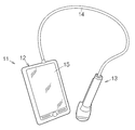
図1は本発明の一実施形態に係る電子機器の一具体例すなわち超音波診断装置(超音波画像装置)11の構成を概略的に示す。超音波診断装置11は装置端末(処理部)12と超音波プローブ(プローブ)13とを備える。装置端末12と超音波プローブ13とはケーブル14で相互に接続される。装置端末12と超音波プローブ13とはケーブル14を通じて電気信号をやりとりする。装置端末12にはディスプレイパネル(表示装置)15が組み込まれる。ディスプレイパネル15の画面は装置端末12の表面で露出する。装置端末12では、超音波プローブ13で検出された超音波に基づき画像が生成される。画像化された検出結果がディスプレイパネル15の画面に表示される。
(1) Overall Configuration of Ultrasonic Diagnostic Apparatus FIG. 1 schematically shows a specific example of an electronic apparatus, that is, an ultrasonic diagnostic apparatus (ultrasonic imaging apparatus) 11 according to an embodiment of the present invention. The ultrasonic
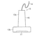
図2に示されるように、超音波プローブ13は筐体16を有する。筐体16内には超音波デバイス17が収容される。超音波デバイス17の表面は筐体16の表面で露出することができる。超音波デバイス17は表面から超音波を出力するとともに超音波の反射波を受信する。その他、超音波プローブ13は、プローブ本体13aに着脱自在に連結されるプローブヘッド13bを備えることができる。このとき、超音波デバイス17はプローブヘッド13bの筐体16内に組み込まれることができる。
As shown in FIG. 2, the
図3は超音波デバイス17の平面図を概略的に示す。超音波デバイス17は基体21を備える。基体21には素子アレイ22が形成される。素子アレイ22はアレイ状に配置された薄膜型超音波トランスデューサー素子(以下「素子」という)23の配列で構成される。配列は複数行複数列のマトリクスで形成される。その他、配列では千鳥配置が確立されてもよい。千鳥配置では偶数列の素子23群は奇数列の素子23群に対して行ピッチの2分の1でずらされればよい。奇数列および偶数列の一方の素子数は他方の素子数に比べて1つ少なくてもよい。
FIG. 3 schematically shows a plan view of the
個々の素子23は振動膜24を備える。図3では振動膜24の膜面に直交する方向の平面視(基板の厚み方向からの平面視)で振動膜24の輪郭が点線で描かれる。振動膜24上には圧電素子25が形成される。圧電素子25は上電極26、下電極27および圧電体膜28で構成される。個々の素子23ごとに上電極26および下電極27の間に圧電体膜28が挟まれる。これらは下電極27、圧電体膜28および上電極26の順番で重ねられる。超音波デバイス17は1枚の超音波トランスデューサー素子チップ(基板)として構成される。
Each
基体21の表面には複数本の第1導電体29が形成される。第1導電体29は配列の行方向に相互に平行に延びる。1行の素子23ごとに1本の第1導電体29が割り当てられる。1本の第1導電体29は配列の行方向に並ぶ素子23の圧電体膜28に共通に接続される。第1導電体29は個々の素子23ごとに上電極26を形成する。第1導電体29の両端は1対の引き出し配線31にそれぞれ接続される。引き出し配線31は配列の列方向に相互に平行に延びる。したがって、全ての第1導電体29は同一長さを有する。こうしてマトリクス全体の素子23に共通に上電極26は接続される。第1導電体29は例えばイリジウム(Ir)で形成されることができる。ただし、第1導電体29にはその他の導電材が利用されてもよい。
A plurality of
基体21の表面には複数本の第2導電体32が形成される。第2導電体32は配列の列方向に相互に平行に延びる。1列の素子23ごとに1本の第2導電体32が割り当てられる。1本の第2導電体32は配列の列方向に並ぶ素子23の圧電体膜28に共通に配置される。第2導電体32は個々の素子23ごとに下電極27を形成する。第2導電体32には例えばチタン(Ti)、イリジウム(Ir)、白金(Pt)およびチタン(Ti)の積層膜が用いられることができる。ただし、第2導電体32にはその他の導電材が利用されてもよい。
A plurality of
列ごとに素子23の通電は切り替えられる。こうした通電の切り替えに応じてリニアスキャンやセクタースキャンは実現される。1列の素子23は同時に超音波を出力することから、1列の個数すなわち配列の行数は超音波の出力レベルに応じて決定されることができる。行数は例えば10〜15行程度に設定されればよい。図中では省略されて5行が描かれる。配列の列数はスキャンの範囲の広がりに応じて決定されることができる。列数は例えば128列や256列に設定されればよい。図中では省略されて8列が描かれる。上電極26および下電極27の役割は入れ替えられてもよい。すなわち、マトリクス全体の素子23に共通に下電極が接続される一方で、配列の列ごとに共通に素子23に上電極が接続されてもよい。
Energization of the
基体21の輪郭は、相互に平行な1対の直線で仕切られて対向する第1辺21aおよび第2辺21bを有する。第1辺21aと素子アレイ22の輪郭との間に1ラインの第1端子アレイ33aが配置される。第2辺21bと素子アレイ22の輪郭との間に1ラインの第2端子アレイ33bが配置される。第1端子アレイ33aは第1辺21aに平行に1ラインを形成することができる。第2端子アレイ33bは第2辺21bに平行に1ラインを形成することができる。第1端子アレイ33aは1対の上電極端子34および複数の下電極端子35で構成される。同様に、第2端子アレイ33bは1対の上電極端子36および複数の下電極端子37で構成される。1本の引き出し配線31の両端にそれぞれ上電極端子34、36は接続される。引き出し配線31および上電極端子34、36は素子アレイ22を二等分する垂直面で面対称に形成されればよい。1本の第2導電体32の両端にそれぞれ下電極端子35、37は接続される。第2導電体32および下電極端子35、37は素子アレイ22を二等分する垂直面で面対称に形成されればよい。ここでは、基体21の輪郭は矩形に形成される。基体21の輪郭は正方形であってもよく台形であってもよい。
The outline of the
基体21には第1フレキシブルプリント配線板(以下「第1配線板」という)38が連結される。第1配線板38は第1端子アレイ33aに覆い被さる。第1配線板38の一端には上電極端子34および下電極端子35に個別に対応して導電線すなわち第1信号線39が形成される。第1信号線39は上電極端子34および下電極端子35に個別に向き合わせられ個別に接合される。同様に、基体21には第2フレキシブルプリント配線板(以下「第2配線板」という)41が覆い被さる。第2配線板41は第2端子アレイ33bに覆い被さる。第2配線板41の一端には上電極端子36および下電極端子37に個別に対応して導電線すなわち第2信号線42が形成される。第2信号線42は上電極端子36および下電極端子37に個別に向き合わせられ個別に接合される。
A first flexible printed wiring board (hereinafter referred to as “first wiring board”) 38 is connected to the
図4に示されるように、基体21は基板44および被覆膜45を備える。基板44の表面に被覆膜45が一面に形成される。基板44には個々の素子23ごとに開口46が形成される。開口46は基板44に対してアレイ状に配置される。開口46が配置される領域の輪郭は素子アレイ22の輪郭に相当する。隣接する2つの開口46の間には仕切り壁47が区画される。隣接する開口46は仕切り壁47で仕切られる。仕切り壁47の壁厚みは開口46の間隔に相当する。仕切り壁47は相互に平行に広がる平面内に2つの壁面を規定する。壁厚みは2つの壁面の距離に相当する。すなわち、壁厚みは壁面に直交して壁面の間に挟まれる垂線の長さで規定されることができる。基板44は例えばシリコン基板で形成されればよい。
As shown in FIG. 4, the
被覆膜45は、基板44の表面に積層される酸化シリコン(SiO2)層48と、酸化シリコン層48の表面に積層される酸化ジルコニウム(ZrO2)層49とで構成される。被覆膜45は開口46に接する。こうして開口46の輪郭に対応して被覆膜45の一部が振動膜24を形成する。振動膜24は、被覆膜45のうち、開口46に臨むことから基板44の厚み方向に膜振動することができる部分である。酸化シリコン層48の膜厚は共振周波数に基づき決定されることができる。
The covering
振動膜24の表面に下電極27、圧電体膜28および上電極26が順番に積層される。圧電体膜28は例えばジルコン酸チタン酸鉛(PZT)で形成されることができる。圧電体膜28にはその他の圧電材料が用いられてもよい。ここでは、第1導電体29の下で圧電体膜28は完全に第2導電体32を覆う。圧電体膜28の働きで第1導電体29と第2導電体32との間で短絡は回避されることができる。
A
基体21の表面には音響整合層51が積層される。音響整合層51は素子アレイ22を覆う。音響整合層51の膜厚は振動膜24の共振周波数に応じて決定される。音響整合層51には例えばシリコーン樹脂膜が用いられることができる。音響整合層51は第1端子アレイ33aおよび第2端子アレイ33bの間の空間に収まる。音響整合層51の縁は基体21の第1辺21aおよび第2辺21bから離れる。音響整合層51は基体21の輪郭よりも小さい輪郭を有する。
An
音響整合層51上には音響レンズ52が配置される。音響レンズ52の輪郭は音響整合層51の輪郭に重なる。したがって、音響レンズ52の縁は基体21の第1辺21aおよび第2辺21bから離れる。音響レンズ52は音響整合層51の表面に密着する。音響レンズ52は音響整合層51の働きで基体21に接着される。音響レンズ52の外表面は部分円筒面で形成される。部分円筒面は第1導電体29に平行な母線を有する。部分円筒面の曲率は、1筋の第2導電体33に接続される1列の素子23から発信される超音波の焦点位置に応じて決定される。音響レンズ52は例えばシリコーン樹脂から形成される。音響レンズ52は生体の音響インピーダンスに近い音響インピーダンスを有する。
An
基体21には保護膜53が固定される。保護膜53は例えばエポキシ樹脂といった遮水性を有する素材から形成される。ただし、保護膜53はその他の樹脂材から形成されてもよい。保護膜53は音響レンズ52および音響整合層51に接触する。ここでは、保護膜53は音響レンズ52および音響整合層51の側面52a、51aに固着される。側面52a、51aは基体21の表面に垂直に基体21の表面から立ち上がる。図4では、保護膜53は、音響レンズ52の母線に平行に広がり基体21に直角に交差する2つの仮想平面54a、54bにそれぞれ沿った接触面53aで音響レンズ52および音響整合層51を挟む。このとき、音響レンズ52および音響整合層51の側面52a、51aは面一に広がる。保護膜53は、音響整合層51と第1および第2配線板38、41との間で基体21表面の第2導電体32や引き出し配線31に被さる。同様に、保護膜53は、基体21上で第1配線板38および第2配線板41の端部に被さる。
A
基体21の裏面にはバッキング材56が固定される。バッキング材56の表面に基体21の裏面が重ねられる。バッキング材56は超音波デバイス17の裏面で開口46を閉じる。バッキング材56はリジッドな基材を備えることができる。ここでは、仕切り壁47はバッキング材56に結合される。バッキング材56は個々の仕切り壁47に少なくとも1カ所の接合域で接合される。接合にあたって接着剤は用いられることができる。
A
(2)第1実施形態に係る音響整合層
図5に示されるように、第1実施形態に係る音響整合層51は母材57とフィラー58とを備える。フィラー58は母材57内で分散する。母材57はシリコーン樹脂で形成される。フィラー58には例えば酸化亜鉛粉末、酸化ジルコニウム粉末、アルミナ粉末、シリカ粉末、酸化チタン粉末、炭化珪素粉末、窒化アルミニウム粉末、カーボン粉末および窒化ボロン粉末の群から選択される少なくとも1つが用いられる。母材57は、素子23の振動膜24の範囲で広がる第1域57aと、隣り合う素子23同士の間で広がる第2域57bとを有する。第2域57bは第1域57a同士を接続する。第1域57aではフィラー58は第1値の平均粒径を有する。第2域57bではフィラー58は第1値よりも大きい第2値の平均粒径を有する。ここでは、単位体積当たりのフィラー58の個数は概ね等しい。その結果、基体21の厚み方向の平面視で、素子23の範囲に比べて、隣り合う素子23の間の領域で単位体積当たりのフィラー58の占有体積の割合は大きい。ここでは、音響整合層51内の第1域57aは圧電素子25から遠ざかるにつれて広がる。
(2) Acoustic matching layer according to the first embodiment As shown in FIG. 5, the
(3)超音波デバイスの動作
次に超音波診断装置11の動作を簡単に説明する。超音波の送信にあたって圧電素子25にはパルス信号が供給される。パルス信号は下電極端子35、37および上電極端子34、36を通じて列ごとに素子23に供給される。個々の素子23では下電極27および上電極26の間で圧電体膜28に電界が作用する。圧電体膜28は超音波の周波数で振動する。圧電体膜28の振動は振動膜24に伝わる。こうして振動膜24は超音波振動する。その結果、対象物(例えば人体の内部)に向けて所望の超音波ビームは発せられる。
(3) Operation of Ultrasonic Device Next, the operation of the ultrasonic
超音波の反射波は振動膜24を振動させる。振動膜24の超音波振動は所望の周波数で圧電体膜28を超音波振動させる。圧電素子25の圧電効果に応じて圧電素子25から電圧が出力される。個々の素子23では上電極26と下電極27との間で電位が生成される。電位は下電極端子35、37および上電極端子34、36から電気信号として出力される。こうして超音波は検出される。
The ultrasonic reflected wave vibrates the
超音波の送信および受信は繰り返される。その結果、リニアスキャンやセクタースキャンは実現される。スキャンが完了すると、出力信号のデジタル信号に基づき画像が形成される。形成された画像はディスプレイパネル15の画面に表示される。
Transmission and reception of ultrasonic waves are repeated. As a result, linear scan and sector scan are realized. When the scan is completed, an image is formed based on the digital signal of the output signal. The formed image is displayed on the screen of the
超音波の発信時に素子23が超音波振動すると、超音波は素子23から音響整合層51を伝わり音響レンズ52の表面から出射される。このとき、音響レンズ52は生体の音響インピーダンスに近い音響インピーダンスを有することから、音響レンズ52および生体の間の界面で超音波の反射は抑制される。音響整合層51は素子23と生体との間で音響インピーダンスの整合を図る。音響インピーダンスの整合の結果、音響整合層51の界面で超音波の反射は低減される。
When the
隣り合う素子23では一方の素子23から他方の素子23に向かって音響整合層51内を超音波振動が伝搬する。隣り合う素子23の間ではフィラー58の占有体積の割合が大きいことから、超音波振動は効率的に減衰する。一方の素子23から他方の素子23に向かって超音波振動の伝搬は防止される。こうして隣り合う素子23同士の間でクロストークは防止される。隣り合う素子23同士の間では音響整合層51の母材57は連続することから、超音波振動の反射は抑制される。超音波の乱反射は抑制される。超音波測定の精度は向上する。
In
超音波振動は素子23から広がりながら音響整合層51内を伝搬する。前述のように、音響整合層51内でフィラー58の占有体積が小さい第1域57aが圧電素子25から遠ざかるにつれて広がれば、フィラー58の占有体積の高い第2域57bに進入する超音波振動は抑制される。こうして超音波の乱反射はさらに効果的に抑制される。
The ultrasonic vibration propagates in the
(4)超音波デバイスの製造方法
次に超音波デバイス17の製造方法を簡単に説明する。図6に示されるように、基板61が用意される。基板61は、基材62上にアレイ状に配置された複数の素子23を含む素子アレイ22を有する。基材62は前述の基体21に相当する。基材62には開口46が形成される。基材62の裏面にはバッキング材56が接合される。基板61には第1配線板38および第2配線板41が固着される。
(4) Method for Manufacturing Ultrasonic Device Next, a method for manufacturing the
その後、基板61の表面に音響整合層51が形成される。音響整合層51の形成にあたって、まず、図7に示されるように、基板61の厚み方向の平面視で隣り合う素子23の間の領域に第1素材63が塗布される。第1素材63の塗布にあたって例えばインクジェット技術が利用されることができる。第1素材63の液滴は表面張力の働きで基板61の表面から遠ざかるにつれて先細る。第1素材63ではシリコーン樹脂の流動体64にフィラー58が分散する。第1素材63ではフィラー58は第2値の平均粒径を有する。塗布された第1素材63を半硬化させる。
Thereafter, the
続いて、図8に示されるように、隣り合う第1素材63同士の間の領域に第2素材65が塗布される。第2素材65の塗布にあたって同様にインクジェット技術が用いられればよい。第2素材65は第1素材63同士の間の空間を満たす。第2素材65ではシリコーン樹脂の流動体66にフィラー58が分散する。第2素材65ではフィラー58は第1値の平均粒径を有する。第1素材63および第2素材65で単位体積当たりのフィラー58の粒子数が概ね等しければ、第1素材63では、第2素材65に比べて、流動体66内で単位体積当たりのフィラー58の占有体積の割合は大きい。
Subsequently, as shown in FIG. 8, the
第2素材65が塗布されると、第1素材63および第2素材65上に音響レンズ52が設置される。音響レンズ52は第1素材63および第2素材65に密着する。第1素材63および第2素材65が硬化すると、音響レンズ52は基板61に固定される。第1素材63は音響整合層51の第2域57bに相当し、第2素材65は音響整合層51の第1域57aに相当する。
When the
このとき、第1素材63は基板61の表面から遠ざかるにつれて先細る形状に形成されることから、第1素材の半硬化などに応じて第1素材63と第2素材65との混合が防止されると、第2素材65は素子23から遠ざかるにつれて広がる形状に形成されることができる。フィラー58の占有体積の割合が小さい領域は素子23から遠ざかるにつれて広がるような形状を有することができる。
At this time, since the
(5)第2実施形態に係る音響整合層
図9に示されるように、第2実施形態に係る音響整合層71は母材72とフィラー73a、73bとを備える。フィラー73a、73bは母材72内で分散する。母材72はシリコーン樹脂で形成される。母材72は音響整合層71の全域で連続する。フィラー73a、73bには例えば酸化亜鉛粉末、酸化ジルコニウム粉末、アルミナ粉末、シリカ粉末、酸化チタン粉末、炭化珪素粉末、窒化アルミニウム粉末、カーボン粉末および窒化ボロン粉末の群から選択される少なくとも1つが用いられる。第1フィラー73aは第1値の平均粒径を有する。第2フィラー73bは第1値よりも大きい第2値の平均粒径を有する。第1フィラー73aは素子23の振動膜24の範囲に偏在する。第2フィラー73bは隣り合う素子23同士の間の領域に偏在する。ここでは、単位体積当たりの第1フィラー73aおよび第2フィラー73bの個数は概ね等しい。その結果、基体21の厚み方向の平面視で、素子23の範囲に比べて、隣り合う素子23の間で単位体積当たりのフィラーの占有体積の割合は大きい。こういった音響整合層71は前述の音響整合層51に代えて超音波デバイス17に組み入れられる。
(5) Acoustic matching layer according to the second embodiment As shown in FIG. 9, the
超音波の発信時に、隣り合う素子23では一方の素子23から他方の素子23に向かって音響整合層71内を超音波振動が伝搬する。隣り合う素子23の間では第1フィラー73aに比べて第2フィラー73bの占有体積の割合が大きいことから、超音波振動は効率的に減衰する。一方の素子23から他方の素子23に向かって超音波振動の伝搬は防止される。こうして隣り合う素子23同士の間でクロストークは防止される。隣り合う素子23同士の間では音響整合層71の母材72は連続することから、超音波振動の反射は抑制される。超音波の乱反射は抑制される。超音波測定の精度は向上する。
When transmitting ultrasonic waves, ultrasonic vibration propagates in the
超音波デバイス17の製造にあたって基板61の表面に音響整合層71が形成される。音響整合層71の形成にあたって、まず、図10に示されるように、基板61の表面に流動性の素材75が塗布される。素材75には第1フィラー73aおよび第2フィラー73bが包含される。第1フィラー73aは第1値の粒径範囲の粉末で形成される。第2フィラー73bは第1値よりも大きい第2値の粒径範囲の粉末で形成される。素材75は素子アレイ22を覆う。
In manufacturing the
素材75の塗布後、個々の素子23で超音波振動を発生させる。図11に示されるように、素材75内で定在波76が発生する。選択された特定の周波数で超音波振動が付与されると、第2フィラー73bは、超音波振動に基づき、振動膜24の領域から隣り合う振動膜24同士の間の領域に向かって移動する。こうして第2フィラー73bは隣り合う振動膜24同士の間の領域に偏在する。
After the
超音波振動の印加時間が調整されることで、第2フィラー73bの占有体積の割合は勾配を有することができる。振動膜24の領域から、隣り合う振動膜24同士の間の領域に向かって徐々に第2フィラー73bの占有体積の割合は変化する。その結果、音響整合層71内で音響インピーダンスの急激な変化は回避される。したがって、音響インピーダンスの急激な変化に基づく超音波振動の反射は効果的に抑制される。こうして超音波の乱反射は確実に抑制される。
By adjusting the application time of the ultrasonic vibration, the ratio of the occupied volume of the
その他、図12および図13に示されるように、音響整合層51、71では占有体積の割合の調整にあたってフィラー77の個数が利用されることができる。母材78中には概ね等しい粒径のフィラー77が分散する。振動膜24の領域ではフィラー77の個数が少なく、隣り合う振動膜24同士の間の領域ではフィラー77の個数が多い。フィラー77の個数が増大すれば、占有体積の割合は高まって、音響整合層51、71を伝搬する超音波振動の減衰は促進される。隣り合う素子23同士の間でクロストークは防止される。
In addition, as shown in FIGS. 12 and 13, in the acoustic matching layers 51 and 71, the number of
なお、上記のように本実施形態について詳細に説明したが、本発明の新規事項および効果から実体的に逸脱しない多くの変形が可能であることは当業者には容易に理解できるであろう。したがって、このような変形例はすべて本発明の範囲に含まれる。例えば、明細書または図面において、少なくとも一度、より広義または同義な異なる用語とともに記載された用語は、明細書または図面のいかなる箇所においても、その異なる用語に置き換えられることができる。また、超音波診断装置11や装置端末12、超音波プローブ13、ディスプレイパネル15、筐体16、基体21、素子23、第1および第2配線板38、41、音響整合層51、71、音響レンズ52等の構成および動作も本実施形態で説明したものに限定されず、種々の変形が可能である。
Although the present embodiment has been described in detail as described above, it will be easily understood by those skilled in the art that many modifications can be made without departing from the novel matters and effects of the present invention. Therefore, all such modifications are included in the scope of the present invention. For example, a term described with a different term having a broader meaning or the same meaning at least once in the specification or the drawings can be replaced with the different term in any part of the specification or the drawings. In addition, the ultrasonic
11 電子機器および超音波画像装置としての超音波診断装置、12 処理部(装置端末)、13 プローブ(超音波プローブ)、13a プローブ本体、13b プローブヘッド、15 表示装置(ディスプレイパネル)、16 筐体、17 超音波デバイス、22 素子アレイ、23 超音波トランスデューサー素子、44 基材(基板)、51 音響整合層、57 母材、57a 第1域、57b 第2域、58 フィラー、63 第1素材、65 第2素材、71 音響整合層、72 母材、73a 第1フィラー、73b 第2フィラー、77 フィラー、78 母材。
DESCRIPTION OF
Claims (11)
母材およびフィラーで形成されて、前記複数の超音波トランスデューサー素子を覆う音響整合層と、
前記基板の厚み方向の平面視で、前記超音波トランスデューサー素子の範囲に比べて、隣り合う前記超音波トランスデューサー素子の間で単位体積当たりの前記フィラーの占有体積の割合は大きい
ことを特徴とする超音波デバイス。 A substrate having an ultrasonic transducer elements of multiple,
An acoustic matching layer formed of a base material and a filler and covering the plurality of ultrasonic transducer elements ;
The ratio of the occupied volume of the filler per unit volume between the adjacent ultrasonic transducer elements is larger than the range of the ultrasonic transducer elements in a plan view in the thickness direction of the substrate, Ultrasonic device to do.
前記超音波トランスデューサー素子が配置される領域内に第2素材を塗布する工程と、
を備え、
前記第1素材では、前記第2素材に比べて、母材内で単位体積当たりのフィラーの占有体積の割合が大きい
ことを特徴とする超音波デバイスの製造方法。 A substrate having an ultrasonic transducer element of several, applying a first material in a region between the ultrasonic transducer elements adjacent to each other in plan view in the thickness direction of the substrate,
Applying a second material in a region where the ultrasonic transducer element is disposed;
With
The method of manufacturing an ultrasonic device, wherein the first material has a larger proportion of filler volume per unit volume in the base material than the second material.
個々の前記超音波トランスデューサー素子で超音波振動を発生させ、前記超音波振動に基づき、前記基板の厚み方向からの平面視で前記超音波トランスデューサー素子の範囲から隣り合う前記超音波トランスデューサー素子同士の間に領域に向かって前記第2フィラーを移動させ、隣り合う前記超音波トランスデューサー素子同士の間の領域に前記第2フィラーを偏在させる工程と、
を備えることを特徴とする超音波デバイスの製造方法。
A substrate having an ultrasonic transducer element of several, applying flowable material including a second filler of the first filler and the particle size range of the first value is greater than the second value of the particle size range of the first value And covering the plurality of ultrasonic transducer elements with the material,
Each ultrasonic transducer element generates ultrasonic vibrations, and based on the ultrasonic vibrations, the ultrasonic transducer elements that are adjacent from the range of the ultrasonic transducer elements in plan view from the thickness direction of the substrate Moving the second filler toward the region between them, and unevenly distributing the second filler in a region between the adjacent ultrasonic transducer elements;
An ultrasonic device manufacturing method comprising:
Priority Applications (1)
| Application Number | Priority Date | Filing Date | Title |
|---|---|---|---|
| JP2014037269A JP6252248B2 (en) | 2014-02-27 | 2014-02-27 | Ultrasonic device, manufacturing method thereof, probe, electronic apparatus, and ultrasonic imaging apparatus |
Applications Claiming Priority (1)
| Application Number | Priority Date | Filing Date | Title |
|---|---|---|---|
| JP2014037269A JP6252248B2 (en) | 2014-02-27 | 2014-02-27 | Ultrasonic device, manufacturing method thereof, probe, electronic apparatus, and ultrasonic imaging apparatus |
Publications (3)
| Publication Number | Publication Date |
|---|---|
| JP2015162813A JP2015162813A (en) | 2015-09-07 |
| JP2015162813A5 JP2015162813A5 (en) | 2017-03-23 |
| JP6252248B2 true JP6252248B2 (en) | 2017-12-27 |
Family
ID=54185633
Family Applications (1)
| Application Number | Title | Priority Date | Filing Date |
|---|---|---|---|
| JP2014037269A Active JP6252248B2 (en) | 2014-02-27 | 2014-02-27 | Ultrasonic device, manufacturing method thereof, probe, electronic apparatus, and ultrasonic imaging apparatus |
Country Status (1)
| Country | Link |
|---|---|
| JP (1) | JP6252248B2 (en) |
Families Citing this family (2)
| Publication number | Priority date | Publication date | Assignee | Title |
|---|---|---|---|---|
| JP6468426B2 (en) * | 2014-03-10 | 2019-02-13 | セイコーエプソン株式会社 | Ultrasonic sensor |
| JP2017092097A (en) | 2015-11-04 | 2017-05-25 | セイコーエプソン株式会社 | Piezoelectric element, ultrasonic probe, ultrasonic measuring device and manufacturing method of piezoelectric element |
Family Cites Families (3)
| Publication number | Priority date | Publication date | Assignee | Title |
|---|---|---|---|---|
| JP4787630B2 (en) * | 2006-03-03 | 2011-10-05 | 日立アロカメディカル株式会社 | Ultrasonic probe |
| US20080021328A1 (en) * | 2006-07-20 | 2008-01-24 | Konica Minolta Medical & Graphic, Inc. | Ultrasound probe and method of manufacturing ultrasound probe |
| JP5261152B2 (en) * | 2008-11-27 | 2013-08-14 | 日立アロカメディカル株式会社 | Ultrasonic transducer |
-
2014
- 2014-02-27 JP JP2014037269A patent/JP6252248B2/en active Active
Also Published As
| Publication number | Publication date |
|---|---|
| JP2015162813A (en) | 2015-09-07 |
Similar Documents
| Publication | Publication Date | Title |
|---|---|---|
| US10707407B2 (en) | Ultrasonic device, method for manufacturing the same, electronic device and ultrasonic imaging device | |
| US9184370B2 (en) | Ultrasonic transducer device, ultrasonic measurement apparatus, head unit, probe, and ultrasonic imaging apparatus | |
| JP5990930B2 (en) | Ultrasonic transducer element chip and probe, electronic device and ultrasonic diagnostic apparatus | |
| US10086405B2 (en) | Piezoelectric element, piezoelectric device, probe, electronic machine, and ultrasonic image apparatus | |
| JP6252130B2 (en) | Ultrasonic device, manufacturing method thereof, electronic apparatus, and ultrasonic imaging apparatus | |
| JP6442821B2 (en) | Ultrasonic device and electronic equipment | |
| JP6299509B2 (en) | Ultrasonic device and probe, electronic apparatus and ultrasonic imaging apparatus | |
| JP6326833B2 (en) | Ultrasonic device, method for manufacturing ultrasonic device, probe, electronic device, ultrasonic imaging apparatus | |
| JP6299511B2 (en) | Ultrasonic device and probe and electronic equipment | |
| JP6314777B2 (en) | Ultrasonic sensor and probe and electronic equipment | |
| JP6273743B2 (en) | Ultrasonic device and probe, electronic apparatus and ultrasonic imaging apparatus | |
| JP6221582B2 (en) | Ultrasonic device and probe, electronic apparatus and ultrasonic imaging apparatus | |
| US20130338502A1 (en) | Ultrasonic transducer element package, ultrasonic transducer element chip, probe, probe head, electronic device, ultrasonic diagnostic apparatus, and method for producing ultrasonic transducer element package | |
| JP6252279B2 (en) | ULTRASONIC TRANSDUCER DEVICE AND PROBE, ELECTRONIC DEVICE, AND ULTRASONIC IMAGING DEVICE | |
| JP2016033970A (en) | Ultrasonic device and method for manufacturing the same, and probe and electronic equipment | |
| JP2014195494A (en) | Ultrasonic transducer device, probe, electronic device, and ultrasonic image device | |
| JP6252248B2 (en) | Ultrasonic device, manufacturing method thereof, probe, electronic apparatus, and ultrasonic imaging apparatus | |
| JP2015160104A (en) | Ultrasonic device unit, probe, electronic device and ultrasonic image apparatus | |
| JP2016032572A (en) | Manufacturing method of acoustic coupling member | |
| JP2014124431A (en) | Acoustic lens, head unit, probe, ultrasonic imaging device, and correction member | |
| JP2017000792A (en) | Ultrasonic transducer element chip, probe, electronic device, and ultrasonic diagnostic device | |
| JP2017170156A (en) | Ultrasonic transducer device and electronic apparatus | |
| JP2014197735A (en) | Ultrasonic transducer device, probe, electronic apparatus and ultrasonic image device | |
| JP2016092591A (en) | Ultrasonic device unit, probe and electronic apparatus | |
| JP2017029571A (en) | Piezoelectric device, probe, electronic apparatus, and ultrasound imaging apparatus |
Legal Events
| Date | Code | Title | Description |
|---|---|---|---|
| A521 | Written amendment |
Free format text: JAPANESE INTERMEDIATE CODE: A523 Effective date: 20170220 |
|
| A621 | Written request for application examination |
Free format text: JAPANESE INTERMEDIATE CODE: A621 Effective date: 20170220 |
|
| A977 | Report on retrieval |
Free format text: JAPANESE INTERMEDIATE CODE: A971007 Effective date: 20171023 |
|
| TRDD | Decision of grant or rejection written | ||
| A01 | Written decision to grant a patent or to grant a registration (utility model) |
Free format text: JAPANESE INTERMEDIATE CODE: A01 Effective date: 20171031 |
|
| A61 | First payment of annual fees (during grant procedure) |
Free format text: JAPANESE INTERMEDIATE CODE: A61 Effective date: 20171113 |
|
| R150 | Certificate of patent or registration of utility model |
Ref document number: 6252248 Country of ref document: JP Free format text: JAPANESE INTERMEDIATE CODE: R150 |