JP6242553B1 - Polyphase filter and filter circuit - Google Patents
Polyphase filter and filter circuit Download PDFInfo
- Publication number
- JP6242553B1 JP6242553B1 JP2017545976A JP2017545976A JP6242553B1 JP 6242553 B1 JP6242553 B1 JP 6242553B1 JP 2017545976 A JP2017545976 A JP 2017545976A JP 2017545976 A JP2017545976 A JP 2017545976A JP 6242553 B1 JP6242553 B1 JP 6242553B1
- Authority
- JP
- Japan
- Prior art keywords
- output terminal
- phase
- variable capacitor
- end connected
- variable
- Prior art date
- Legal status (The legal status is an assumption and is not a legal conclusion. Google has not performed a legal analysis and makes no representation as to the accuracy of the status listed.)
- Active
Links
Images


Classifications
-
- H—ELECTRICITY
- H03—ELECTRONIC CIRCUITRY
- H03H—IMPEDANCE NETWORKS, e.g. RESONANT CIRCUITS; RESONATORS
- H03H11/00—Networks using active elements
- H03H11/02—Multiple-port networks
- H03H11/04—Frequency selective two-port networks
- H03H11/12—Frequency selective two-port networks using amplifiers with feedback
-
- H—ELECTRICITY
- H03—ELECTRONIC CIRCUITRY
- H03H—IMPEDANCE NETWORKS, e.g. RESONANT CIRCUITS; RESONATORS
- H03H11/00—Networks using active elements
- H03H11/02—Multiple-port networks
- H03H11/16—Networks for phase shifting
- H03H11/22—Networks for phase shifting providing two or more phase shifted output signals, e.g. n-phase output
-
- H—ELECTRICITY
- H03—ELECTRONIC CIRCUITRY
- H03H—IMPEDANCE NETWORKS, e.g. RESONANT CIRCUITS; RESONATORS
- H03H7/00—Multiple-port networks comprising only passive electrical elements as network components
- H03H7/18—Networks for phase shifting
- H03H7/21—Networks for phase shifting providing two or more phase shifted output signals, e.g. n-phase output
-
- H—ELECTRICITY
- H03—ELECTRONIC CIRCUITRY
- H03H—IMPEDANCE NETWORKS, e.g. RESONANT CIRCUITS; RESONATORS
- H03H11/00—Networks using active elements
- H03H11/02—Multiple-port networks
- H03H11/16—Networks for phase shifting
- H03H11/20—Two-port phase shifters providing an adjustable phase shift
-
- H—ELECTRICITY
- H03—ELECTRONIC CIRCUITRY
- H03H—IMPEDANCE NETWORKS, e.g. RESONANT CIRCUITS; RESONATORS
- H03H7/00—Multiple-port networks comprising only passive electrical elements as network components
- H03H7/01—Frequency selective two-port networks
- H03H2007/0192—Complex filters
-
- H—ELECTRICITY
- H03—ELECTRONIC CIRCUITRY
- H03H—IMPEDANCE NETWORKS, e.g. RESONANT CIRCUITS; RESONATORS
- H03H2210/00—Indexing scheme relating to details of tunable filters
- H03H2210/02—Variable filter component
- H03H2210/021—Amplifier, e.g. transconductance amplifier
-
- H—ELECTRICITY
- H03—ELECTRONIC CIRCUITRY
- H03H—IMPEDANCE NETWORKS, e.g. RESONANT CIRCUITS; RESONATORS
- H03H2210/00—Indexing scheme relating to details of tunable filters
- H03H2210/02—Variable filter component
- H03H2210/025—Capacitor
Landscapes
- Networks Using Active Elements (AREA)
- Filters And Equalizers (AREA)
Abstract
1段構成で低い挿入損失を実現しつつ、振幅整合および位相整合を実現することができるポリフェーズフィルタを得る。第1可変抵抗および第2可変抵抗は、互いに等しい抵抗値を有し、この抵抗値は、第1出力端子から第4出力端子までの出力のうち、直交する信号間の振幅誤差を補正するように設定され、第1可変容量、第2可変容量、第3可変容量および第4可変容量は、互いに等しい容量値を有し、この容量値は、第1出力端子から第4出力端子までの出力のうち、直交する信号間の位相誤差を補正するように設定されている。A polyphase filter capable of realizing amplitude matching and phase matching while achieving low insertion loss with a single-stage configuration is obtained. The first variable resistor and the second variable resistor have the same resistance value, and this resistance value corrects an amplitude error between orthogonal signals among the outputs from the first output terminal to the fourth output terminal. The first variable capacitor, the second variable capacitor, the third variable capacitor, and the fourth variable capacitor have the same capacitance value, and this capacitance value is output from the first output terminal to the fourth output terminal. Of these, the phase error between orthogonal signals is set to be corrected.
Description
この発明は、I/Q直交信号を生成するポリフェーズフィルタ、およびポリフェーズフィルタを用いたフィルタ回路に関する。 The present invention relates to a polyphase filter for generating an I / Q quadrature signal and a filter circuit using the polyphase filter.
従来から、IRM(Image Rejection Mixer)やベクトル合成形移相器に用いられるI/Q直交信号生成器として、ポリフェーズフィルタが知られている。ポリフェーズフィルタは、抵抗および容量により構成され、ベクトル合成形移相器の内部でI/Q直交信号を生成する機能を有しており、低い挿入損失、高い振幅精度および位相精度が求められる。なお、一般的に、位相精度を向上させるために、ポリフェーズフィルタを多段にする手法がとられるが、挿入損失が劣化するという問題がある。 Conventionally, a polyphase filter is known as an I / Q quadrature signal generator used for an IRM (Image Rejection Mixer) or a vector synthesis type phase shifter. The polyphase filter is configured by a resistor and a capacitor, and has a function of generating an I / Q quadrature signal inside the vector synthesis type phase shifter. Low insertion loss, high amplitude accuracy, and phase accuracy are required. In general, in order to improve the phase accuracy, a multi-phase filter is used, but there is a problem that the insertion loss is deteriorated.
ここで、このようなポリフェーズフィルタとして、出力される振幅誤差を補正するように、抵抗値および容量値を設定する振幅整合型ポリフェーズフィルタが提案されている。さらに、振幅整合型ポリフェーズフィルタと多段ポリフェーズフィルタとを組み合わせることで、振幅整合および位相整合を実現したポリフェーズフィルタが提案されている(例えば、特許文献1参照)。 Here, as such a polyphase filter, an amplitude matching polyphase filter in which a resistance value and a capacitance value are set so as to correct an output amplitude error has been proposed. Furthermore, there has been proposed a polyphase filter that realizes amplitude matching and phase matching by combining an amplitude matching polyphase filter and a multistage polyphase filter (see, for example, Patent Document 1).
また、ポリフェーズフィルタを多段にすることなく位相精度を向上させるために、容量として可変容量であるバラクタを用いることで、高い位相精度を実現したポリフェーズフィルタが提案されている(例えば、非特許文献1参照)。 Further, in order to improve the phase accuracy without increasing the number of polyphase filters, there has been proposed a polyphase filter that realizes high phase accuracy by using a varactor that is a variable capacitor as a capacitor (for example, non-patent) Reference 1).
しかしながら、従来技術には、以下のような課題がある。
すなわち、特許文献1では、可変抵抗と固定容量とを組み合わせて振幅整合型ポリフェーズフィルタを構成しているので、可変抵抗の抵抗値を調整することにより振幅誤差は補正できるものの、位相誤差を補正することができないという問題がある。また、位相誤差を補正するために、振幅整合型ポリフェーズフィルタを多段ポリフェーズフィルタと組み合わせた場合には、上述したように挿入損失が劣化するという問題がある。However, the prior art has the following problems.
That is, in
また、非特許文献1では、固定抵抗とバラクタとを組み合わせてポリフェーズフィルタを構成しているので、バラクタの容量値を調整することにより位相誤差は補正できるものの、バラクタは特に高周波領域においてQ値が低下する特性を有している。そのため、高周波領域ではバラクタに等価的に直列抵抗が接続されたようになるので、出力される直交信号間に振幅誤差が生じる恐れがあるという問題がある。
In
また、特許文献1のポリフェーズフィルタと非特許文献1のポリフェーズフィルタとを組み合わせることにより、振幅誤差および位相誤差を補正することが考えられるが、ポリフェーズフィルタが2段構成となってしまうので、上述したように挿入損失が劣化するという問題がある。
Further, it is conceivable to correct the amplitude error and the phase error by combining the polyphase filter of
この発明は、上記のような課題を解決するためになされたものであり、1段構成で低い挿入損失を実現しつつ、振幅整合および位相整合を実現することができるポリフェーズフィルタを得ることを目的とする。 The present invention has been made to solve the above-described problems, and is to obtain a polyphase filter capable of realizing amplitude matching and phase matching while realizing low insertion loss with a single-stage configuration. Objective.
この発明に係るポリフェーズフィルタは、一端が第1入力端子に、他端が第1出力端子にそれぞれ接続された第1固定抵抗と、一端が第1入力端子に、他端が第2出力端子にそれぞれ接続された第1可変抵抗と、一端が第2入力端子に、他端が第3出力端子にそれぞれ接続された第2固定抵抗と、一端が第2入力端子に、他端が第4出力端子にそれぞれ接続された第2可変抵抗と、一端が第2入力端子に、他端が第1出力端子にそれぞれ接続された第1可変容量と、一端が第1入力端子に、他端が第2出力端子にそれぞれ接続された第2可変容量と、一端が第1入力端子に、他端が第3出力端子にそれぞれ接続された第3可変容量と、一端が第2入力端子に、他端が第4出力端子にそれぞれ接続された第4可変容量と、を備え、第1可変抵抗および第2可変抵抗は、互いに等しい抵抗値を有し、この抵抗値は、第1出力端子から第4出力端子までの出力のうち、直交する信号間の振幅誤差を補正するように設定され、第1可変容量、第2可変容量、第3可変容量および第4可変容量は、互いに等しい容量値を有し、この容量値は、第1出力端子から第4出力端子までの出力のうち、直交する信号間の位相誤差を補正するように設定されているものである。 The polyphase filter according to the present invention includes a first fixed resistor having one end connected to the first input terminal and the other end connected to the first output terminal, one end connected to the first input terminal, and the other end connected to the second output terminal. A first variable resistor connected to the second input terminal, one end connected to the second input terminal, the other fixed terminal connected to the third output terminal, one end connected to the second input terminal, and the other end connected to the fourth input terminal. A second variable resistor connected to the output terminal; a first variable capacitor having one end connected to the second input terminal; the other end connected to the first output terminal; one end connected to the first input terminal; A second variable capacitor connected to the second output terminal; a third variable capacitor connected at one end to the first input terminal; the other end connected to the third output terminal; and one end connected to the second input terminal; A fourth variable capacitor having an end connected to the fourth output terminal, respectively, and a first variable resistor And the second variable resistor have resistance values equal to each other, and the resistance value is set so as to correct an amplitude error between orthogonal signals among outputs from the first output terminal to the fourth output terminal, The first variable capacitor, the second variable capacitor, the third variable capacitor, and the fourth variable capacitor have the same capacitance value, and this capacitance value is orthogonal among the outputs from the first output terminal to the fourth output terminal. It is set so as to correct the phase error between the signals to be processed.
この発明に係るポリフェーズフィルタによれば、第1可変抵抗および第2可変抵抗は、互いに等しい抵抗値を有し、この抵抗値は、第1出力端子から第4出力端子までの出力のうち、直交する信号間の振幅誤差を補正するように設定され、第1可変容量、第2可変容量、第3可変容量および第4可変容量は、互いに等しい容量値を有し、この容量値は、第1出力端子から第4出力端子までの出力のうち、直交する信号間の位相誤差を補正するように設定されている。
そのため、1段構成で低い挿入損失を実現しつつ、振幅整合および位相整合を実現することができる。According to the polyphase filter of the present invention, the first variable resistor and the second variable resistor have the same resistance value, and the resistance value is the output from the first output terminal to the fourth output terminal. The first variable capacitor, the second variable capacitor, the third variable capacitor, and the fourth variable capacitor are set to correct an amplitude error between orthogonal signals, and have the same capacitance value. Of the outputs from the first output terminal to the fourth output terminal, the phase error between orthogonal signals is set to be corrected.
Therefore, it is possible to realize amplitude matching and phase matching while realizing low insertion loss with a one-stage configuration.
以下、この発明に係るポリフェーズフィルタおよびフィルタ回路の好適な実施の形態につき図面を用いて説明するが、各図において同一、または相当する部分については、同一符号を付して説明する。 Hereinafter, preferred embodiments of a polyphase filter and a filter circuit according to the present invention will be described with reference to the drawings. In the drawings, the same or corresponding parts will be described with the same reference numerals.
まず、実施の形態の説明に先立って、図1〜4を参照しながら、上述した従来のポリフェーズフィルタにおける問題について詳細に説明する。なお、図1〜3は、非特許文献1のポリフェーズフィルタに関連し、図4は、特許文献1のポリフェーズフィルタに関連している。
First, prior to the description of the embodiment, problems in the above-described conventional polyphase filter will be described in detail with reference to FIGS. 1 to 3 relate to the polyphase filter of Non-Patent
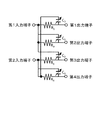
図1は、従来のポリフェーズフィルタの問題を説明するための回路図である。図1において、このポリフェーズフィルタは、4個の固定抵抗R0と4個のバラクタC0とから構成されている。FIG. 1 is a circuit diagram for explaining a problem of a conventional polyphase filter. In FIG. 1, the polyphase filter is composed of four fixed resistors R 0 and four varactors C 0 .
また、差動信号が第1入力端子および第2入力端子に入力され、出力される直交信号のうち、I差動信号が第1出力端子および第3出力端子から出力され、Q差動信号が第2出力端子および第4出力端子から出力される。ここで、プロセスや温度等のばらつきにより、出力される直交信号に位相誤差が生じることがある。 Of the orthogonal signals that are input to and output from the first input terminal and the second input terminal, the I differential signal is output from the first output terminal and the third output terminal, and the Q differential signal is Output from the second output terminal and the fourth output terminal. Here, a phase error may occur in the output quadrature signal due to variations in process, temperature, and the like.
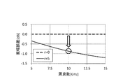
このとき、バラクタC0の容量値を調整することにより、位相誤差を補正することができる。しかしながら、バラクタC0は特に高周波領域においてQ値が低下する特性を有しているので、高周波領域では、図2に示されるように、バラクタC0に等価的に直列抵抗rが接続されたように見える。そのため、出力される直交信号間に振幅誤差が生じる恐れがあるという問題がある。At this time, the phase error can be corrected by adjusting the capacitance value of the varactor C 0 . However, since the varactor C 0 has a characteristic that the Q value decreases particularly in the high frequency region, as shown in FIG. 2, the series resistor r is equivalently connected to the varactor C 0 in the high frequency region. Looks like. Therefore, there is a problem that an amplitude error may occur between the output orthogonal signals.
例えば、10GHzにおいてバラクタC0のQ値が10と低い値を示す場合に、バラクタC0には、等価的に抵抗r=5Ωが直列に接続されたものと考えられる。ここで、図3に示されるように、10GHzにおいて位相誤差を0degに設定した場合に、r=0ΩのときはI/Q直交信号の振幅誤差が0dBであるのに対して、r=5Ωとしたときは、I/Q直交信号の振幅誤差が0.9dBとなってしまう。For example, when the Q value of the varactor C 0 is as low as 10 at 10 GHz, it is considered that the resistance r = 5Ω is equivalently connected in series to the varactor C 0 . Here, as shown in FIG. 3, when the phase error is set to 0 deg at 10 GHz, when r = 0Ω, the amplitude error of the I / Q quadrature signal is 0 dB, whereas r = 5Ω. In this case, the amplitude error of the I / Q quadrature signal becomes 0.9 dB.
このように、図1に示した従来の1段構成のポリフェーズフィルタでは、抵抗値を固定にして、バラクタC0の容量値を調整することで位相誤差を補正しているものの、振幅誤差は補正することができないという問題がある。Thus, in the conventional single-phase polyphase filter shown in FIG. 1, although the resistance value is fixed and the phase error is corrected by adjusting the capacitance value of the varactor C 0 , the amplitude error is There is a problem that it cannot be corrected.
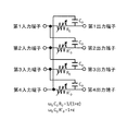
図4は、従来のポリフェーズフィルタの問題を説明するための回路図である。図4において、このポリフェーズフィルタは、2個の可変抵抗R0および2個の可変抵抗R’0と4個の固定容量C0とから構成されている。FIG. 4 is a circuit diagram for explaining the problem of the conventional polyphase filter. In FIG. 4, the polyphase filter is composed of two variable resistors R 0, two variable resistors R ′ 0, and four fixed capacitors C 0 .
ここで、第2入力端子および第4入力端子への差動入力信号の振幅が、振幅誤差をεとして第1入力端子および第3入力端子への差動入力信号の振幅の(1+ε)倍大きく位相誤差が90度である場合について考える。 Here, the amplitude of the differential input signal to the second input terminal and the fourth input terminal is (1 + ε) times larger than the amplitude of the differential input signal to the first input terminal and the third input terminal, where ε is the amplitude error. Consider the case where the phase error is 90 degrees.
このとき、固定容量C0は変化させずに、可変抵抗R0の抵抗値を振幅誤差がない場合の抵抗値の(1+ε)分の1倍に、可変抵抗R’0の抵抗値を振幅誤差がない場合の抵抗値の(1+ε)倍にすることにより、振幅誤差を補正することができる。At this time, without changing the fixed capacitor C 0, the resistance value of the variable resistor R 0 is set to one times (1 + ε) of the resistance value when there is no amplitude error, and the resistance value of the variable resistor R ′ 0 is changed to the amplitude error. By making the resistance value (1 + ε) times as large as there is not, the amplitude error can be corrected.
なお、これらの制御は、IF信号の角周波数をω0とした場合に、ω0C0R0=1/(1+ε)およびω0C0R’0=1+εを満たすことで成り立つことから、容量C0または抵抗R0のどちらかを固定にしないと制御することができない。Note that these controls are satisfied by satisfying ω 0 C 0 R 0 = 1 / (1 + ε) and ω 0 C 0 R ′ 0 = 1 + ε when the angular frequency of the IF signal is ω 0 . Control is not possible unless either the capacitance C 0 or the resistance R 0 is fixed.
このように、図4に示した従来の1段構成のポリフェーズフィルタでは、容量値を固定にして、可変抵抗の抵抗値を調整することで振幅誤差のみを補正しているので、位相誤差は補正することができないという問題がある。 Thus, in the conventional single-phase polyphase filter shown in FIG. 4, only the amplitude error is corrected by fixing the capacitance value and adjusting the resistance value of the variable resistor. There is a problem that it cannot be corrected.
また、図1に示した従来のポリフェーズフィルタと図4に示した従来のポリフェーズフィルタとを組み合わせることにより、振幅誤差および位相誤差を0にして、振幅整合および位相整合を実現することが考えられるが、ポリフェーズフィルタが2段構成となってしまうので、低い挿入損失を実現することができないという問題がある。 Further, it is conceivable to realize amplitude matching and phase matching by combining the conventional polyphase filter shown in FIG. 1 and the conventional polyphase filter shown in FIG. 4 with zero amplitude error and phase error. However, since the polyphase filter has a two-stage configuration, there is a problem that a low insertion loss cannot be realized.
そこで、以下の実施の形態では、1段構成で低い挿入損失を実現しつつ、振幅整合および位相整合を実現することができるポリフェーズフィルタ、およびポリフェーズフィルタを用いたフィルタ回路について説明する。 Therefore, in the following embodiments, a polyphase filter capable of realizing amplitude matching and phase matching while realizing low insertion loss with a single-stage configuration, and a filter circuit using the polyphase filter will be described.
実施の形態1.
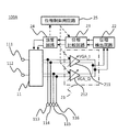
図5は、この発明の実施の形態1に係るポリフェーズフィルタを用いたフィルタ回路を示す回路図である。図5において、このフィルタ回路100は、ポリフェーズフィルタ11、振幅比較回路12、第1演算回路13、位相比較回路14および第2演算回路15を備えている。
FIG. 5 is a circuit diagram showing a filter circuit using the polyphase filter according to
ポリフェーズフィルタ11は、第1固定抵抗および第2固定抵抗からなる2個の固定抵抗R1並びに第1可変抵抗および第2可変抵抗からなる2個の可変抵抗R2と、第1可変容量、第2可変容量、第3可変容量および第4可変容量からなる4個の可変容量C1とから構成されている。The
また、第1固定抵抗R1の一端が第1入力端子に、他端が第1出力端子にそれぞれ接続され、第1可変抵抗R2の一端が第1入力端子に、他端が第2出力端子にそれぞれ接続され、第2固定抵抗R1の一端が第2入力端子に、他端が第3出力端子にそれぞれ接続され、第2可変抵抗R2の一端が第2入力端子に、他端が第4出力端子にそれぞれ接続されている。Also, one end of the first fixed resistor R 1 is connected to the first input terminal, the other end is connected to the first output terminal, one end of the first variable resistor R 2 is connected to the first input terminal, and the other end is the second output. One end of the second fixed resistor R 1 is connected to the second input terminal, the other end is connected to the third output terminal, and one end of the second variable resistor R 2 is connected to the second input terminal. Are respectively connected to the fourth output terminals.
また、第1可変容量C1の一端が第2入力端子に、他端が第1出力端子にそれぞれ接続され、第2可変容量C1の一端が第1入力端子に、他端が第2出力端子にそれぞれ接続され、第3可変容量C1の一端が第1入力端子に、他端が第3出力端子にそれぞれ接続され、第4可変容量C1の一端が第2入力端子に、他端が第4出力端子にそれぞれ接続されている。Also, one end of the first variable capacitor C 1 is connected to the second input terminal, the other end is connected to the first output terminal, one end of the second variable capacitor C 1 is connected to the first input terminal, and the other end is the second output. One end of the third variable capacitor C 1 is connected to the first input terminal, the other end is connected to the third output terminal, and one end of the fourth variable capacitor C 1 is connected to the second input terminal. Are respectively connected to the fourth output terminals.
ここで、ポリフェーズフィルタ11は、第1可変抵抗R2および第2可変抵抗R2が、互いに等しい抵抗値を有し、この抵抗値が、第1出力端子から第4出力端子までの出力のうち、直交する信号間の振幅誤差を補正するように設定され、第1可変容量C1、第2可変容量C1、第3可変容量C1および第4可変容量C1が、互いに等しい容量値を有し、この容量値が、第1出力端子から第4出力端子までの出力のうち、直交する信号間の位相誤差を補正するように設定されて、振幅位相整合型ポリフェーズフィルタを構成している。Here, in the
振幅比較回路12は、第3出力端子および第4出力端子から出力される直交信号が入力され、比較結果を示す信号が第1演算回路13に出力される。第1演算回路13は、振幅比較回路12からの信号が入力され、第1可変抵抗R2および第2可変抵抗R2に制御信号を出力する。The
位相比較回路14は、第1出力端子および第2出力端子から出力される直交信号が入力され、比較結果を示す信号が第2演算回路15に出力される。第2演算回路15は、位相比較回路14からの信号が入力され、第1可変容量C1、第2可変容量C1、第3可変容量C1および第4可変容量C1に制御信号を出力する。The
以下、上記構成のフィルタ回路100の動作について説明する。
振幅比較回路12は、第3出力端子および第4出力端子から出力される直交信号に基づいて、振幅誤差εを検出する。ここで、振幅誤差εは、入力信号のばらつきや温度ばらつき、プロセスばらつき等の要因で動的に変動する値であり、入力端子に理想差動信号が入力された場合は、ε=0となる。Hereinafter, the operation of the
The
第1演算回路13は、振幅比較回路12で検出された振幅誤差εを用いて、第1可変抵抗R2および第2可変抵抗R2を最適化する。このとき、可変容量C1のQ値が低く、等価的に直列抵抗rが接続されていると仮定すると、振幅誤差εと可変抵抗R2との間には、次式(1)の関係が成立する。The first
ε=√[{(r/R1)2+(R2/r)2}/2]−1・・・(1)ε = √ [{(r / R 1 ) 2 + (R 2 / r) 2 } / 2] −1 (1)
式(1)において、振幅誤差εが0に近い領域では、振幅誤差εは、可変抵抗R2に対して単調増加特性を示している。すなわち、第1演算回路13は、振幅誤差εが0になるように可変抵抗R2の値を繰り返し制御することで、値を収束させることができる。In the equation (1), in the region where the amplitude error ε is close to 0, the amplitude error ε exhibits a monotonically increasing characteristic with respect to the variable resistor R 2 . That is, the first
位相比較回路14は、第1出力端子および第2出力端子から出力される直交信号に基づいて、位相誤差θを検出する。ここで、入力信号のばらつきや温度ばらつき、プロセスばらつき等の要因で振幅誤差θは動的に変動する値であり、入力端子に理想差動信号が入力された場合はθ=0となる。
The
第2演算回路15は、位相比較回路14で検出された位相誤差θを用いて、第1可変容量C1、第2可変容量C1、第3可変容量C1および第4可変容量C1を最適化する。このとき、位相誤差θと可変容量C1との間には、次式(2)の関係が成立する。The second
tanθ={(ωC1)2×R1R2+1}/{(ωC1)2×R1R2−1}・・・(2)tan θ = {(ωC 1 ) 2 × R 1 R 2 +1} / {(ωC 1 ) 2 × R 1 R 2 −1} (2)
すなわち、第2演算回路15は、振幅誤差θが0になるように可変容量C1の値を繰り返し制御することで、値を収束させることができる。ここで、式(1)に示されるように、振幅誤差εは可変容量C1に依存しないため、θ=0となるように可変容量C1を制御しても、振幅誤差εには影響しない。That is, the second
なお、動的に変動する振幅誤差εに応じて、これらの可変抵抗R2および可変容量C1を最適化する手順が行われるので、可変抵抗R2および可変容量C1も動的に変動することになる。In addition, since the procedure for optimizing the variable resistor R 2 and the variable capacitor C 1 is performed according to the dynamically varying amplitude error ε, the variable resistor R 2 and the variable capacitor C 1 also dynamically vary. It will be.
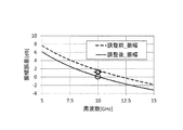
図6および図7は、この発明の実施の形態1に係るポリフェーズフィルタを用いたフィルタ回路の効果を説明するためのグラフである。なお、図6は振幅誤差特性を示し、図7は位相誤差特性を示している。 6 and 7 are graphs for explaining the effect of the filter circuit using the polyphase filter according to the first embodiment of the present invention. 6 shows the amplitude error characteristic, and FIG. 7 shows the phase error characteristic.
図6、7において、例えばある素子定数の場合(調整前)に、10GHzにおいて振幅誤差1.9dB、位相誤差5.6degの特性が得られているとする。ここで、上述した方法により可変抵抗R2および可変容量C1を制御すると、図に示すように、振幅誤差を0dB、位相誤差0deg(位相誤差90deg)に補正することができた。6 and 7, for example, in the case of a certain element constant (before adjustment), it is assumed that characteristics of an amplitude error of 1.9 dB and a phase error of 5.6 deg are obtained at 10 GHz. Here, when the variable resistor R 2 and the variable capacitor C 1 were controlled by the method described above, the amplitude error could be corrected to 0 dB and the
このように、ポリフェーズフィルタ11は、出力端での直交信号間の振幅誤差を振幅比較回路12で比較し、振幅誤差を補正するように可変抵抗R2を調整することによって、I/Q直交信号の振幅整合を実現するとともに、出力端での直交信号間の位相誤差を位相比較回路14で比較し、位相誤差を補正するように可変容量C1を調整することによって、I/Q直交信号の位相整合を実現している。また、この手順で制御を行うことにより、振幅整合および位相整合を同時に実現することができる。Thus, the
以上のように、実施の形態1によれば、ポリフェーズフィルタにおいて、第1可変抵抗および第2可変抵抗は、互いに等しい抵抗値を有し、この抵抗値は、第1出力端子から第4出力端子までの出力のうち、直交する信号間の振幅誤差を補正するように設定され、第1可変容量、第2可変容量、第3可変容量および第4可変容量は、互いに等しい容量値を有し、この容量値は、第1出力端子から第4出力端子までの出力のうち、直交する信号間の位相誤差を補正するように設定されている。
そのため、1段構成で低い挿入損失を実現しつつ、振幅整合および位相整合を実現することができる。As described above, according to the first embodiment, in the polyphase filter, the first variable resistor and the second variable resistor have the same resistance value, and this resistance value is output from the first output terminal to the fourth output. It is set to correct the amplitude error between the orthogonal signals among the outputs up to the terminals, and the first variable capacitor, the second variable capacitor, the third variable capacitor, and the fourth variable capacitor have the same capacitance value. The capacitance value is set so as to correct a phase error between orthogonal signals among outputs from the first output terminal to the fourth output terminal.
Therefore, it is possible to realize amplitude matching and phase matching while realizing low insertion loss with a one-stage configuration.
実施の形態2.
図8は、この発明の実施の形態2に係るポリフェーズフィルタを用いたフィルタ回路を示す回路図である。図8において、このフィルタ回路100Aは、ポリフェーズフィルタ11、ベクトル合成形移相器21、位相検出回路22、位相比較回路23、演算回路24および位相制御用回路25を備えている。
FIG. 8 is a circuit diagram showing a filter circuit using the polyphase filter according to
ポリフェーズフィルタ11は、上記実施の形態1で示したものと同一の構成を有する振幅位相整合型ポリフェーズフィルタであり、入力側に入力端子111、112が接続され、出力側に出力端子113〜116が接続されている。出力端子113〜116からは、4本の直交差動信号が出力され、分岐してベクトル合成形移相器21に入力される。
The
ベクトル合成形移相器21は、VGA_I211およびVGA_Q212から構成されている。ここで、VGAは、Variable Gain Amplifierの略である。VGA_I211およびVGA_Q212は、ポリフェーズフィルタ11からのI/Q直交差動信号および位相制御用回路25からの制御信号がそれぞれ入力され、直交信号を合成して位相検出回路22に出力する。
The vector composition
位相検出回路22の入力側は、ベクトル合成形移相器21の出力側に接続され、位相検出回路22の出力側は、位相比較回路23の入力側に接続されている。また、位相比較回路23の入力側は、位相検出回路22の出力側に接続され、位相比較回路23の出力側は、演算回路24の入力側に接続されている。
The input side of the
演算回路24の入力側は、位相比較回路23の出力側に接続され、演算回路24の出力側は、ポリフェーズフィルタ11に接続されている。また、位相制御用回路25の入力側は、演算回路24の出力側に接続され、位相制御用回路25の出力側は、位相比較回路23、VGA_I211およびVGA_Q212に接続されている。
The input side of the
ここで、演算回路24は、位相比較回路23からの信号が入力され、ポリフェーズフィルタ11に制御信号を出力するとともに、位相制御用回路25にも制御信号を出力する。また、位相制御用回路25は、VGA_I211およびVGA_Q212のみならず、位相比較回路23にも制御信号を出力する。
Here, the
以下、上記構成のフィルタ回路100Aの動作について説明する。
ポリフェーズフィルタ11は、入力端子111、112から入力された差動信号をI/Q直交差動信号に変換する。ここで、ポリフェーズフィルタ11の素子ばらつきにより、振幅誤差εおよび位相誤差θが生じているとする。Hereinafter, the operation of the
The
なお、振幅誤差εおよび位相誤差θは、入力信号のばらつきや温度ばらつき、プロセスばらつき等の要因で動的に変動する値であり、入力端子に理想差動信号が入力された場合は、ε=0およびθ=0となる。また、振幅誤差εおよび位相誤差θは、後述するベクトル合成形移相器21および演算回路24等で構成されるループにより補正される。具体的な補正手順は、以下の通りである。
Note that the amplitude error ε and phase error θ are values that dynamically change due to factors such as input signal variations, temperature variations, process variations, and the like, when an ideal differential signal is input to the input terminal, ε = 0 and θ = 0. Further, the amplitude error ε and the phase error θ are corrected by a loop composed of a vector composition
まず、演算回路24は、ベクトル合成形移相器21の移相量を、0〜360度まで複数のポイントでスイープする。また、ベクトル合成形移相器21は、位相制御用回路25を通して与えられたVGAの位相設定値に従って動作し、出力の位相を決定する。ただし、ポリフェーズフィルタ11には、上述したように振幅誤差εおよび位相誤差θが生じているため、出力信号の位相は、位相設定値からの誤差を含んでいる。
First, the
続いて、この振幅誤差εおよび位相誤差θを、位相検出回路22および位相比較回路23により検出する。ここで、位相比較回路23の比較結果を演算回路24に入力することで、ベクトル合成形移相器21の誤差特性を求めることができ、その誤差特性から逆算することで、ポリフェーズフィルタ11の振幅誤差εおよび位相誤差θを算出することができる。
Subsequently, the amplitude error ε and the phase error θ are detected by the
次に、算出された振幅誤差εおよび位相誤差θを用いて、上記実施の形態1で示した方法により、ポリフェーズフィルタ11の可変抵抗R2および可変容量C1の値を最適化する。これにより、ポリフェーズフィルタ11の振幅誤差および位相誤差を補正することができる。Next, using the calculated amplitude error ε and phase error θ, the values of the variable resistor R 2 and the variable capacitor C 1 of the
なお、動的に変動する振幅誤差εに応じて、これらの可変抵抗R2および可変容量C1を最適化する手順が行われるので、可変抵抗R2および可変容量C1も動的に変動することになる。In addition, since the procedure for optimizing the variable resistor R 2 and the variable capacitor C 1 is performed according to the dynamically varying amplitude error ε, the variable resistor R 2 and the variable capacitor C 1 also dynamically vary. It will be.
以上のように、実施の形態2によれば、ポリフェーズフィルタにおいて、第1可変抵抗および第2可変抵抗は、互いに等しい抵抗値を有し、この抵抗値は、第1出力端子から第4出力端子までの出力のうち、直交する信号間の振幅誤差を補正するように設定され、第1可変容量、第2可変容量、第3可変容量および第4可変容量は、互いに等しい容量値を有し、この容量値は、第1出力端子から第4出力端子までの出力のうち、直交する信号間の位相誤差を補正するように設定されている。
そのため、1段構成で低い挿入損失を実現しつつ、振幅整合および位相整合を実現することができる。As described above, according to the second embodiment, in the polyphase filter, the first variable resistor and the second variable resistor have the same resistance value, and the resistance value is output from the first output terminal to the fourth output. It is set to correct the amplitude error between the orthogonal signals among the outputs up to the terminals, and the first variable capacitor, the second variable capacitor, the third variable capacitor, and the fourth variable capacitor have the same capacitance value. The capacitance value is set so as to correct a phase error between orthogonal signals among outputs from the first output terminal to the fourth output terminal.
Therefore, it is possible to realize amplitude matching and phase matching while realizing low insertion loss with a one-stage configuration.
Claims (3)
一端が第1入力端子に、他端が第2出力端子にそれぞれ接続された第1可変抵抗と、
一端が第2入力端子に、他端が第3出力端子にそれぞれ接続された第2固定抵抗と、
一端が第2入力端子に、他端が第4出力端子にそれぞれ接続された第2可変抵抗と、
一端が第2入力端子に、他端が第1出力端子にそれぞれ接続された第1可変容量と、
一端が第1入力端子に、他端が第2出力端子にそれぞれ接続された第2可変容量と、
一端が第1入力端子に、他端が第3出力端子にそれぞれ接続された第3可変容量と、
一端が第2入力端子に、他端が第4出力端子にそれぞれ接続された第4可変容量と、を備え、
前記第1可変抵抗および前記第2可変抵抗は、互いに等しい抵抗値を有し、この抵抗値は、前記第1出力端子から前記第4出力端子までの出力のうち、直交する信号間の振幅誤差を補正するように設定され、
前記第1可変容量、前記第2可変容量、前記第3可変容量および前記第4可変容量は、互いに等しい容量値を有し、この容量値は、前記第1出力端子から前記第4出力端子までの出力のうち、直交する信号間の位相誤差を補正するように設定されている
ポリフェーズフィルタ。A first fixed resistor having one end connected to the first input terminal and the other end connected to the first output terminal;
A first variable resistor having one end connected to the first input terminal and the other end connected to the second output terminal;
A second fixed resistor having one end connected to the second input terminal and the other end connected to the third output terminal;
A second variable resistor having one end connected to the second input terminal and the other end connected to the fourth output terminal;
A first variable capacitor having one end connected to the second input terminal and the other end connected to the first output terminal;
A second variable capacitor having one end connected to the first input terminal and the other end connected to the second output terminal;
A third variable capacitor having one end connected to the first input terminal and the other end connected to the third output terminal;
A fourth variable capacitor having one end connected to the second input terminal and the other end connected to the fourth output terminal,
The first variable resistor and the second variable resistor have the same resistance value, and this resistance value is an amplitude error between orthogonal signals among the outputs from the first output terminal to the fourth output terminal. Is set to correct,
The first variable capacitor, the second variable capacitor, the third variable capacitor, and the fourth variable capacitor have the same capacitance value, and the capacitance value is from the first output terminal to the fourth output terminal. A polyphase filter that is set to correct phase errors between orthogonal signals.
前記第1出力端子から前記第4出力端子までの出力のうち、直交する信号間の振幅を比較して、振幅誤差を検出する振幅比較回路と、
前記振幅誤差を補正するように、前記第1可変抵抗および前記第2可変抵抗の抵抗値を演算する第1演算回路と、
前記第1出力端子から前記第4出力端子までの出力のうち、直交する信号間の位相を比較して、位相誤差を検出する振幅比較回路と、
前記第1可変抵抗および前記第2可変抵抗の抵抗値が設定された後に、前記位相誤差を補正するように、前記第1可変容量、前記第2可変容量、前記第3可変容量および前記第4可変容量の容量値を演算する第2演算回路と、
を備えたフィルタ回路。A filter circuit using the polyphase filter according to claim 1,
An amplitude comparison circuit for comparing amplitudes between orthogonal signals among outputs from the first output terminal to the fourth output terminal to detect an amplitude error;
A first arithmetic circuit that calculates resistance values of the first variable resistor and the second variable resistor so as to correct the amplitude error;
An amplitude comparison circuit that detects a phase error by comparing phases between orthogonal signals among outputs from the first output terminal to the fourth output terminal;
After the resistance values of the first variable resistor and the second variable resistor are set, the first variable capacitor, the second variable capacitor, the third variable capacitor, and the fourth variable so as to correct the phase error. A second arithmetic circuit for calculating a capacitance value of the variable capacitor;
Filter circuit with
前記第1出力端子から前記第4出力端子までの出力が入力され、直交する信号を合成して出力するベクトル合成形移相器と、
前記ベクトル合成形移相器で合成された信号の位相を検出する位相検出回路と、
入力された位相設定値に基づいて、前記ベクトル合成形移相器に制御信号を出力する位相制御用回路と、
前記位相検出回路からの出力値と、前記ベクトル合成形移相器に設定された位相設定値とを比較する位相比較回路と、
前記位相比較回路の比較結果に基づいて、前記ポリフェーズフィルタの振幅誤差および位相誤差を算出し、算出された振幅誤差および位相誤差を用いて、前記第1可変抵抗および前記第2可変抵抗の抵抗値、並びに前記第1可変容量、前記第2可変容量、前記第3可変容量および前記第4可変容量の容量値を演算する演算回路と、
を備えたフィルタ回路。A filter circuit using the polyphase filter according to claim 1,
An output from the first output terminal to the fourth output terminal, a vector synthesis type phase shifter that synthesizes and outputs orthogonal signals; and
A phase detection circuit for detecting the phase of the signal synthesized by the vector synthesis phase shifter;
A phase control circuit that outputs a control signal to the vector composition type phase shifter based on the input phase setting value;
A phase comparison circuit that compares an output value from the phase detection circuit with a phase setting value set in the vector composition type phase shifter;
Based on the comparison result of the phase comparison circuit, an amplitude error and a phase error of the polyphase filter are calculated, and the resistances of the first variable resistor and the second variable resistor are calculated using the calculated amplitude error and phase error. An arithmetic circuit for calculating a value and a capacitance value of the first variable capacitor, the second variable capacitor, the third variable capacitor, and the fourth variable capacitor;
Filter circuit with
Applications Claiming Priority (1)
| Application Number | Priority Date | Filing Date | Title |
|---|---|---|---|
| PCT/JP2016/054514 WO2017141367A1 (en) | 2016-02-17 | 2016-02-17 | Poly-phase filter and filter circuit |
Publications (2)
| Publication Number | Publication Date |
|---|---|
| JP6242553B1 true JP6242553B1 (en) | 2017-12-06 |
| JPWO2017141367A1 JPWO2017141367A1 (en) | 2018-02-22 |
Family
ID=59625711
Family Applications (1)
| Application Number | Title | Priority Date | Filing Date |
|---|---|---|---|
| JP2017545976A Active JP6242553B1 (en) | 2016-02-17 | 2016-02-17 | Polyphase filter and filter circuit |
Country Status (5)
| Country | Link |
|---|---|
| US (1) | US10425062B2 (en) |
| EP (1) | EP3419166B1 (en) |
| JP (1) | JP6242553B1 (en) |
| CN (1) | CN108702140B (en) |
| WO (1) | WO2017141367A1 (en) |
Families Citing this family (6)
| Publication number | Priority date | Publication date | Assignee | Title |
|---|---|---|---|---|
| EP3767828B1 (en) * | 2018-04-18 | 2022-09-21 | Mitsubishi Electric Corporation | Polyphase filter |
| US10951202B2 (en) * | 2018-07-20 | 2021-03-16 | Futurewei Technologies, Inc. | Method and apparatus for RC/CR phase error calibration of measurement receiver |
| TWI695581B (en) * | 2019-11-28 | 2020-06-01 | 財團法人工業技術研究院 | Switch-type phase shifter |
| US11271710B1 (en) * | 2020-11-30 | 2022-03-08 | Renesas Electronics Corporation | Wideband quadrature phase generation using tunable polyphase filter |
| US20220182040A1 (en) * | 2020-12-03 | 2022-06-09 | Mediatek Inc. | Filter circuit using polyphase filter with dynamic range enhancement |
| US11811413B2 (en) * | 2021-10-13 | 2023-11-07 | Mediatek Inc. | Poly phase filter with phase error enhance technique |
Citations (9)
| Publication number | Priority date | Publication date | Assignee | Title |
|---|---|---|---|---|
| JPH0229024A (en) * | 1987-12-24 | 1990-01-31 | Fujitsu Ltd | Phase shifter and multiplying circuit |
| JPH1075157A (en) * | 1996-08-30 | 1998-03-17 | Toshiba Corp | 90 degree phase-shifting circuit |
| JP2000013168A (en) * | 1998-06-22 | 2000-01-14 | Nec Corp | Ninety-degree phase shift circuit |
| JP2001119269A (en) * | 1999-10-19 | 2001-04-27 | Nec Corp | 90-degree phase shifter |
| US20040116096A1 (en) * | 2002-12-10 | 2004-06-17 | Irf Semiconductor, Inc. | Radio frequency receiver architecture with tracking image-reject polyphase filtering |
| US20080094133A1 (en) * | 2006-10-18 | 2008-04-24 | Fci Inc. | Poly-phase filter |
| WO2009142201A1 (en) * | 2008-05-19 | 2009-11-26 | 日本電気株式会社 | Device for adjusting band of polyphase filter and method for adjusting band of polyphase filter |
| JP2010021826A (en) * | 2008-07-11 | 2010-01-28 | Seiko Epson Corp | Semiconductor integrated circuit |
| JP2011160214A (en) * | 2010-02-01 | 2011-08-18 | Renesas Electronics Corp | Receiving apparatus and image rejection method |
Family Cites Families (16)
| Publication number | Priority date | Publication date | Assignee | Title |
|---|---|---|---|---|
| FR2647984B1 (en) * | 1989-06-06 | 1991-09-13 | Labo Electronique Physique | IMPROVED PHASE CIRCUIT |
| JPH0818397A (en) * | 1994-06-27 | 1996-01-19 | Hitachi Ltd | 90-degree phase shifter |
| JP3492560B2 (en) * | 1999-07-26 | 2004-02-03 | 日本電信電話株式会社 | Amplitude-matched polyphase filter, phase-amplitude-matched polyphase filter, and image-suppressed receiver |
| US7095801B1 (en) * | 2001-03-30 | 2006-08-22 | Skyworks Solutions, Inc. | Phase adjustable polyphase filters |
| EP1510001B1 (en) * | 2002-06-03 | 2009-02-25 | Telefonaktiebolaget LM Ericsson (publ) | An amplifier circuit, gyrator circuit, filter device and method for amplifying a signal |
| CA2415917A1 (en) * | 2003-01-08 | 2004-07-08 | Sirific Wireless Corporation | Regenerative divider used for up-conversion and down conversion |
| WO2005034350A1 (en) * | 2003-09-30 | 2005-04-14 | Mitsubishi Denki Kabushiki Kaisha | Variable power distributor, its error detecting method and set value correcting method |
| KR101085693B1 (en) * | 2004-03-24 | 2011-11-22 | 조지아 테크 리서치 코오포레이션 | Apparatus for generating improved wideband i/q signal |
| JP4735719B2 (en) * | 2007-03-29 | 2011-07-27 | パナソニック株式会社 | Receiving device and electronic device using the same |
| CN102474236A (en) * | 2009-07-06 | 2012-05-23 | 富士通株式会社 | Polyphase filter and single side band mixer comprising the polyphase filter |
| US9048787B2 (en) * | 2010-04-20 | 2015-06-02 | Rf Micro Devices, Inc. | Combined RF detector and RF attenuator with concurrent outputs |
| JP5633191B2 (en) * | 2010-05-26 | 2014-12-03 | セイコーエプソン株式会社 | Frequency conversion circuit, frequency conversion method, and electronic device |
| CN102832958B (en) * | 2011-06-15 | 2015-02-11 | 硅实验室股份有限公司 | Integrated receivers and integrated circuit having integrated inductors |
| US8760209B2 (en) * | 2012-09-27 | 2014-06-24 | Analog Devices, Inc. | Apparatus and methods for quadrature clock signal generation |
| CN103245960B (en) * | 2013-05-06 | 2015-04-15 | 武汉大学 | Amplifying, mixing and filtering device for GNSS (global navigation satellite system) receiving set |
| US9559792B1 (en) * | 2015-08-31 | 2017-01-31 | Xillinx, Inc. | Broadband in-phase and quadrature phase signal generation |
-
2016
- 2016-02-17 JP JP2017545976A patent/JP6242553B1/en active Active
- 2016-02-17 CN CN201680081875.6A patent/CN108702140B/en active Active
- 2016-02-17 EP EP16890509.9A patent/EP3419166B1/en active Active
- 2016-02-17 US US16/067,701 patent/US10425062B2/en active Active
- 2016-02-17 WO PCT/JP2016/054514 patent/WO2017141367A1/en active Application Filing
Patent Citations (9)
| Publication number | Priority date | Publication date | Assignee | Title |
|---|---|---|---|---|
| JPH0229024A (en) * | 1987-12-24 | 1990-01-31 | Fujitsu Ltd | Phase shifter and multiplying circuit |
| JPH1075157A (en) * | 1996-08-30 | 1998-03-17 | Toshiba Corp | 90 degree phase-shifting circuit |
| JP2000013168A (en) * | 1998-06-22 | 2000-01-14 | Nec Corp | Ninety-degree phase shift circuit |
| JP2001119269A (en) * | 1999-10-19 | 2001-04-27 | Nec Corp | 90-degree phase shifter |
| US20040116096A1 (en) * | 2002-12-10 | 2004-06-17 | Irf Semiconductor, Inc. | Radio frequency receiver architecture with tracking image-reject polyphase filtering |
| US20080094133A1 (en) * | 2006-10-18 | 2008-04-24 | Fci Inc. | Poly-phase filter |
| WO2009142201A1 (en) * | 2008-05-19 | 2009-11-26 | 日本電気株式会社 | Device for adjusting band of polyphase filter and method for adjusting band of polyphase filter |
| JP2010021826A (en) * | 2008-07-11 | 2010-01-28 | Seiko Epson Corp | Semiconductor integrated circuit |
| JP2011160214A (en) * | 2010-02-01 | 2011-08-18 | Renesas Electronics Corp | Receiving apparatus and image rejection method |
Also Published As
| Publication number | Publication date |
|---|---|
| EP3419166A1 (en) | 2018-12-26 |
| US20190013794A1 (en) | 2019-01-10 |
| WO2017141367A1 (en) | 2017-08-24 |
| US10425062B2 (en) | 2019-09-24 |
| CN108702140A (en) | 2018-10-23 |
| JPWO2017141367A1 (en) | 2018-02-22 |
| EP3419166B1 (en) | 2020-01-01 |
| CN108702140B (en) | 2021-07-16 |
| EP3419166A4 (en) | 2019-03-06 |
Similar Documents
| Publication | Publication Date | Title |
|---|---|---|
| JP6242553B1 (en) | Polyphase filter and filter circuit | |
| US9705515B1 (en) | Digital phase locked loop and method of driving the same | |
| US8571161B2 (en) | Electronic device for generating a fractional frequency | |
| US20110189970A1 (en) | Receiving apparatus and image rejection method | |
| US8081936B2 (en) | Method for tuning a digital compensation filter within a transmitter, and associated digital compensation filter and associated calibration circuit | |
| CN114584135A (en) | Wideband quadrature phase generation using tunable polyphase filters | |
| CN108702142B (en) | Phase shift precision correction circuit, vector synthesis type phase shifter and wireless communication machine | |
| EP1236285B1 (en) | Receiver circuit | |
| JP6401902B2 (en) | Orthogonal network and orthogonal signal generation method | |
| US7358802B2 (en) | Multi-phase techniques for tuning and/or measuring operations of an amplifier | |
| US7609123B2 (en) | Direct modulation type voltage-controlled oscillator using MOS varicap | |
| US7482882B2 (en) | Voltage control oscillation circuit and adjusting method for the same | |
| US10944360B2 (en) | Local oscillator | |
| US7126430B2 (en) | PLL circuit | |
| CN111435091B (en) | Self-adaptive phase alignment module and method and vibration gyroscope measurement and control circuit | |
| KR20180131017A (en) | Frequency Synthesizer with Dual Paths for Wideband FMCW | |
| CN114006616A (en) | Self-adaptive phase alignment circuit, debugging method and gyroscope measurement and control circuit | |
| JP2010021826A (en) | Semiconductor integrated circuit | |
| CN111355503A (en) | Compensating device for amplitude modulation and phase modulation distortion | |
| KR100465912B1 (en) | Quadrature signal generator | |
| KR100652809B1 (en) | Wide tunable polyphase filter with variable resistor and variable capacitor | |
| JP3081418B2 (en) | Automatic filter adjustment circuit | |
| CN114513191A (en) | Correction device and method | |
| CN117767942A (en) | Frequency source system and radar | |
| KR100852178B1 (en) | Linearly variable resistor circuit and programmable loop filter including the same |
Legal Events
| Date | Code | Title | Description |
|---|---|---|---|
| A621 | Written request for application examination |
Free format text: JAPANESE INTERMEDIATE CODE: A621 Effective date: 20170831 |
|
| A871 | Explanation of circumstances concerning accelerated examination |
Free format text: JAPANESE INTERMEDIATE CODE: A871 Effective date: 20170831 |
|
| A975 | Report on accelerated examination |
Free format text: JAPANESE INTERMEDIATE CODE: A971005 Effective date: 20170928 |
|
| TRDD | Decision of grant or rejection written | ||
| A01 | Written decision to grant a patent or to grant a registration (utility model) |
Free format text: JAPANESE INTERMEDIATE CODE: A01 Effective date: 20171010 |
|
| A61 | First payment of annual fees (during grant procedure) |
Free format text: JAPANESE INTERMEDIATE CODE: A61 Effective date: 20171107 |
|
| R150 | Certificate of patent or registration of utility model |
Ref document number: 6242553 Country of ref document: JP Free format text: JAPANESE INTERMEDIATE CODE: R150 |
|
| R250 | Receipt of annual fees |
Free format text: JAPANESE INTERMEDIATE CODE: R250 |
|
| R250 | Receipt of annual fees |
Free format text: JAPANESE INTERMEDIATE CODE: R250 |
|
| R250 | Receipt of annual fees |
Free format text: JAPANESE INTERMEDIATE CODE: R250 |
|
| R250 | Receipt of annual fees |
Free format text: JAPANESE INTERMEDIATE CODE: R250 |