JP6239259B2 - System on chip, operation method thereof, and system in package including the same - Google Patents
System on chip, operation method thereof, and system in package including the same Download PDFInfo
- Publication number
- JP6239259B2 JP6239259B2 JP2013097518A JP2013097518A JP6239259B2 JP 6239259 B2 JP6239259 B2 JP 6239259B2 JP 2013097518 A JP2013097518 A JP 2013097518A JP 2013097518 A JP2013097518 A JP 2013097518A JP 6239259 B2 JP6239259 B2 JP 6239259B2
- Authority
- JP
- Japan
- Prior art keywords
- data
- soc
- engine
- encryption
- memory controller
- Prior art date
- Legal status (The legal status is an assumption and is not a legal conclusion. Google has not performed a legal analysis and makes no representation as to the accuracy of the status listed.)
- Active
Links
- 238000000034 method Methods 0.000 title claims description 27
- 230000005540 biological transmission Effects 0.000 claims description 11
- 238000011017 operating method Methods 0.000 claims description 4
- 238000010586 diagram Methods 0.000 description 27
- 238000013478 data encryption standard Methods 0.000 description 2
- 238000005442 molecular electronic Methods 0.000 description 2
- 239000002071 nanotube Substances 0.000 description 2
- 229920000642 polymer Polymers 0.000 description 2
- 230000009365 direct transmission Effects 0.000 description 1
- 230000000694 effects Effects 0.000 description 1
- 238000002347 injection Methods 0.000 description 1
- 239000007924 injection Substances 0.000 description 1
- 238000009413 insulation Methods 0.000 description 1
- 239000012212 insulator Substances 0.000 description 1
- 230000003287 optical effect Effects 0.000 description 1
- 230000037361 pathway Effects 0.000 description 1
- 230000001902 propagating effect Effects 0.000 description 1
- 239000007787 solid Substances 0.000 description 1
- 230000003068 static effect Effects 0.000 description 1
Images


Classifications
-
- G—PHYSICS
- G06—COMPUTING; CALCULATING OR COUNTING
- G06F—ELECTRIC DIGITAL DATA PROCESSING
- G06F21/00—Security arrangements for protecting computers, components thereof, programs or data against unauthorised activity
- G06F21/70—Protecting specific internal or peripheral components, in which the protection of a component leads to protection of the entire computer
- G06F21/71—Protecting specific internal or peripheral components, in which the protection of a component leads to protection of the entire computer to assure secure computing or processing of information
- G06F21/72—Protecting specific internal or peripheral components, in which the protection of a component leads to protection of the entire computer to assure secure computing or processing of information in cryptographic circuits
-
- G—PHYSICS
- G06—COMPUTING; CALCULATING OR COUNTING
- G06F—ELECTRIC DIGITAL DATA PROCESSING
- G06F13/00—Interconnection of, or transfer of information or other signals between, memories, input/output devices or central processing units
- G06F13/14—Handling requests for interconnection or transfer
-
- G—PHYSICS
- G06—COMPUTING; CALCULATING OR COUNTING
- G06F—ELECTRIC DIGITAL DATA PROCESSING
- G06F12/00—Accessing, addressing or allocating within memory systems or architectures
- G06F12/14—Protection against unauthorised use of memory or access to memory
- G06F12/1408—Protection against unauthorised use of memory or access to memory by using cryptography
-
- G—PHYSICS
- G06—COMPUTING; CALCULATING OR COUNTING
- G06F—ELECTRIC DIGITAL DATA PROCESSING
- G06F13/00—Interconnection of, or transfer of information or other signals between, memories, input/output devices or central processing units
- G06F13/14—Handling requests for interconnection or transfer
- G06F13/20—Handling requests for interconnection or transfer for access to input/output bus
- G06F13/28—Handling requests for interconnection or transfer for access to input/output bus using burst mode transfer, e.g. direct memory access DMA, cycle steal
-
- G—PHYSICS
- G06—COMPUTING; CALCULATING OR COUNTING
- G06F—ELECTRIC DIGITAL DATA PROCESSING
- G06F13/00—Interconnection of, or transfer of information or other signals between, memories, input/output devices or central processing units
- G06F13/38—Information transfer, e.g. on bus
-
- G—PHYSICS
- G06—COMPUTING; CALCULATING OR COUNTING
- G06F—ELECTRIC DIGITAL DATA PROCESSING
- G06F21/00—Security arrangements for protecting computers, components thereof, programs or data against unauthorised activity
- G06F21/60—Protecting data
-
- G—PHYSICS
- G06—COMPUTING; CALCULATING OR COUNTING
- G06F—ELECTRIC DIGITAL DATA PROCESSING
- G06F21/00—Security arrangements for protecting computers, components thereof, programs or data against unauthorised activity
- G06F21/60—Protecting data
- G06F21/602—Providing cryptographic facilities or services
-
- G—PHYSICS
- G06—COMPUTING; CALCULATING OR COUNTING
- G06F—ELECTRIC DIGITAL DATA PROCESSING
- G06F21/00—Security arrangements for protecting computers, components thereof, programs or data against unauthorised activity
- G06F21/70—Protecting specific internal or peripheral components, in which the protection of a component leads to protection of the entire computer
- G06F21/71—Protecting specific internal or peripheral components, in which the protection of a component leads to protection of the entire computer to assure secure computing or processing of information
- G06F21/74—Protecting specific internal or peripheral components, in which the protection of a component leads to protection of the entire computer to assure secure computing or processing of information operating in dual or compartmented mode, i.e. at least one secure mode
-
- G—PHYSICS
- G06—COMPUTING; CALCULATING OR COUNTING
- G06F—ELECTRIC DIGITAL DATA PROCESSING
- G06F21/00—Security arrangements for protecting computers, components thereof, programs or data against unauthorised activity
- G06F21/70—Protecting specific internal or peripheral components, in which the protection of a component leads to protection of the entire computer
- G06F21/82—Protecting input, output or interconnection devices
- G06F21/85—Protecting input, output or interconnection devices interconnection devices, e.g. bus-connected or in-line devices
-
- G—PHYSICS
- G06—COMPUTING; CALCULATING OR COUNTING
- G06F—ELECTRIC DIGITAL DATA PROCESSING
- G06F3/00—Input arrangements for transferring data to be processed into a form capable of being handled by the computer; Output arrangements for transferring data from processing unit to output unit, e.g. interface arrangements
- G06F3/06—Digital input from, or digital output to, record carriers, e.g. RAID, emulated record carriers or networked record carriers
- G06F3/0601—Interfaces specially adapted for storage systems
- G06F3/0602—Interfaces specially adapted for storage systems specifically adapted to achieve a particular effect
- G06F3/0614—Improving the reliability of storage systems
- G06F3/0619—Improving the reliability of storage systems in relation to data integrity, e.g. data losses, bit errors
-
- G—PHYSICS
- G06—COMPUTING; CALCULATING OR COUNTING
- G06F—ELECTRIC DIGITAL DATA PROCESSING
- G06F3/00—Input arrangements for transferring data to be processed into a form capable of being handled by the computer; Output arrangements for transferring data from processing unit to output unit, e.g. interface arrangements
- G06F3/06—Digital input from, or digital output to, record carriers, e.g. RAID, emulated record carriers or networked record carriers
- G06F3/0601—Interfaces specially adapted for storage systems
- G06F3/0628—Interfaces specially adapted for storage systems making use of a particular technique
- G06F3/0655—Vertical data movement, i.e. input-output transfer; data movement between one or more hosts and one or more storage devices
-
- G—PHYSICS
- G06—COMPUTING; CALCULATING OR COUNTING
- G06F—ELECTRIC DIGITAL DATA PROCESSING
- G06F3/00—Input arrangements for transferring data to be processed into a form capable of being handled by the computer; Output arrangements for transferring data from processing unit to output unit, e.g. interface arrangements
- G06F3/06—Digital input from, or digital output to, record carriers, e.g. RAID, emulated record carriers or networked record carriers
- G06F3/0601—Interfaces specially adapted for storage systems
- G06F3/0668—Interfaces specially adapted for storage systems adopting a particular infrastructure
- G06F3/0671—In-line storage system
- G06F3/0673—Single storage device
- G06F3/0679—Non-volatile semiconductor memory device, e.g. flash memory, one time programmable memory [OTP]
-
- H—ELECTRICITY
- H04—ELECTRIC COMMUNICATION TECHNIQUE
- H04L—TRANSMISSION OF DIGITAL INFORMATION, e.g. TELEGRAPHIC COMMUNICATION
- H04L9/00—Cryptographic mechanisms or cryptographic arrangements for secret or secure communications; Network security protocols
- H04L9/08—Key distribution or management, e.g. generation, sharing or updating, of cryptographic keys or passwords
- H04L9/0816—Key establishment, i.e. cryptographic processes or cryptographic protocols whereby a shared secret becomes available to two or more parties, for subsequent use
- H04L9/0819—Key transport or distribution, i.e. key establishment techniques where one party creates or otherwise obtains a secret value, and securely transfers it to the other(s)
- H04L9/0822—Key transport or distribution, i.e. key establishment techniques where one party creates or otherwise obtains a secret value, and securely transfers it to the other(s) using key encryption key
-
- G—PHYSICS
- G06—COMPUTING; CALCULATING OR COUNTING
- G06F—ELECTRIC DIGITAL DATA PROCESSING
- G06F2206/00—Indexing scheme related to dedicated interfaces for computers
- G06F2206/10—Indexing scheme related to storage interfaces for computers, indexing schema related to group G06F3/06
- G06F2206/1014—One time programmable [OTP] memory, e.g. PROM, WORM
-
- G—PHYSICS
- G06—COMPUTING; CALCULATING OR COUNTING
- G06F—ELECTRIC DIGITAL DATA PROCESSING
- G06F2212/00—Indexing scheme relating to accessing, addressing or allocation within memory systems or architectures
- G06F2212/10—Providing a specific technical effect
- G06F2212/1052—Security improvement
-
- H—ELECTRICITY
- H04—ELECTRIC COMMUNICATION TECHNIQUE
- H04L—TRANSMISSION OF DIGITAL INFORMATION, e.g. TELEGRAPHIC COMMUNICATION
- H04L2209/00—Additional information or applications relating to cryptographic mechanisms or cryptographic arrangements for secret or secure communication H04L9/00
- H04L2209/12—Details relating to cryptographic hardware or logic circuitry
Landscapes
- Engineering & Computer Science (AREA)
- Theoretical Computer Science (AREA)
- Physics & Mathematics (AREA)
- General Engineering & Computer Science (AREA)
- General Physics & Mathematics (AREA)
- Computer Hardware Design (AREA)
- Computer Security & Cryptography (AREA)
- Software Systems (AREA)
- Mathematical Physics (AREA)
- Human Computer Interaction (AREA)
- Health & Medical Sciences (AREA)
- Bioethics (AREA)
- General Health & Medical Sciences (AREA)
- Signal Processing (AREA)
- Computer Networks & Wireless Communication (AREA)
- Storage Device Security (AREA)
- Combined Controls Of Internal Combustion Engines (AREA)
Description
本発明は、システムオンチップ(System On Chip:SoC)に係り、より詳細には、暗号化/復号化エンジンとメモリコントローラとが直接接続されたシステムオンチップとその動作方法、及びそれを含むシステムインパッケージに関する。 The present invention relates to a system on chip (SoC), more specifically, a system on chip in which an encryption / decryption engine and a memory controller are directly connected, a method of operating the system, and a system including the system Regarding in-package.
メインメモリは、CPU(Central Processing Unit)が実行するプログラムとCPUで必要なデータを、他の記録媒体、例えば不揮発性メモリ装置から受信する。また、メインメモリは、データを保存するために、データを他の記録媒体、例えば不揮発性メモリ装置に伝送する。 The main memory receives a program executed by a CPU (Central Processing Unit) and data necessary for the CPU from another recording medium, for example, a nonvolatile memory device. In addition, the main memory transmits the data to another recording medium, for example, a non-volatile memory device, in order to store the data.
メインメモリと不揮発性メモリ装置との間のデータ送受信過程で、データがプロービング(probing)されることを防止するために、データ送受信途中でデータを暗号化する過程が含まれ得る。メインメモリと不揮発性メモリ装置とを含むシステムの性能は、メインメモリと不揮発性メモリ装置との間でデータを送受信するためのデータ伝送経路、即ちデータパスによって決定される。 In order to prevent the data from being probing in the data transmission / reception process between the main memory and the non-volatile memory device, a process of encrypting the data during the data transmission / reception may be included. The performance of the system including the main memory and the non-volatile memory device is determined by a data transmission path for transmitting and receiving data between the main memory and the non-volatile memory device, that is, a data path.
本発明は、上記従来技術に鑑みてなされたものであって、本発明の目的は、システムオンチップに含まれる暗号化/復号化エンジンとメモリコントローラとを直接接続することによって、データ伝送経路を減少させるシステムオンチップとその動作方法、及びそれを含むシステムインパッケージを提供することにある。 The present invention has been made in view of the above prior art, and an object of the present invention is to directly connect an encryption / decryption engine included in a system-on-chip and a memory controller to thereby establish a data transmission path. An object of the present invention is to provide a system-on-chip to be reduced, a method of operating the same, and a system-in-package including the system-on-chip.
上記目的を達成するためになされた本発明の一態様によるシステムオンチップ(SoC)の動作方法は、前記SoCに含まれるエンジンによって、暗号キーを用いて平文データを暗号文データに変換する段階と、前記エンジンによって、前記暗号文データを前記SoCに含まれるメモリコントローラに直接伝送する段階と、を有し、前記メモリコントローラは、不揮発性メモリの動作を制御する。 A system-on-chip (SoC) operation method according to an aspect of the present invention made to achieve the above object includes a step of converting plaintext data into ciphertext data using an encryption key by an engine included in the SoC. And transmitting the ciphertext data directly to the memory controller included in the SoC by the engine, and the memory controller controls the operation of the nonvolatile memory.
前記SoCの動作方法は、前記平文データを暗号文データに変換する段階の前に、前記平文データをCPUの制御によってメインメモリからバスを介してリードする段階を更に含み得る。 The method of operation of the SoC, prior to the step of converting the plaintext data into ciphertext data, Ru comprise further the step of leading through the bus from the main memory of the plaintext data by the control of the CPU.
上記目的を達成するためになされた本発明の他の態様によるシステムオンチップ(SoC)の動作方法は、前記SoCに含まれるエンジンによって、前記SoCに含まれるメモリコントローラから暗号文データを直接受信する段階と、前記エンジンによって、暗号キーを用いて前記暗号文データを平文データに変換する段階と、を有し、前記メモリコントローラは、不揮発性メモリの動作を制御する。 In order to achieve the above object, a system on chip (SoC) operating method according to another aspect of the present invention directly receives ciphertext data from a memory controller included in the SoC by an engine included in the SoC. And converting the ciphertext data into plaintext data using an encryption key by the engine, and the memory controller controls the operation of the nonvolatile memory.
前記SoCの動作方法は、前記暗号文データを平文データに変換する段階の前に、前記平文データを前記SoCに含まれるDMA(Direct Memory Access)ユニットから前記エンジンに伝送する段階を更に含み得る。 Operation method of the SoC is, prior to the step of converting the ciphertext data into plaintext data further comprises obtain Ru a step of transmitting to the engine from the DMA (Direct Memory Access) unit included the plaintext data to the SoC .
上記目的を達成するためになされた本発明の一態様によるシステムオンチップ(SoC)は、暗号キーを用いて、第1平文データ(plain data)を第1暗号文データ(cipher data)に暗号化し、第2暗号文データを第2平文データに復号化する暗号化/復号化エンジンと、前記暗号化/復号化エンジンに直接接続され、前記第1暗号文データを不揮発性メモリに伝送し、該不揮発性メモリから前記第2暗号文データを受信するメモリコントローラと、を有する。 A system on chip (SoC) according to an aspect of the present invention, which is made to achieve the above object, encrypts first plaintext data (plain data) into first ciphertext data (cipher data) using an encryption key. An encryption / decryption engine for decrypting the second ciphertext data into the second plaintext data, and being directly connected to the encryption / decryption engine, transmitting the first ciphertext data to a non-volatile memory, And a memory controller that receives the second ciphertext data from the nonvolatile memory.
前記SoCは、前記暗号キーを保存するワンタイムプログラマブル(OTP)メモリを更に含み得る。
前記SoCは、前記SoCの外部にある装置から受信した前記第1平文データを前記暗号化/復号化エンジンに伝送し、該暗号化/復号化エンジンから受信した前記第2平文データを前記装置に伝送するDMA(Direct Memory Access)ユニットを更に含み得る。
前記SoCは、前記SoCの外部にある装置と前記暗号化/復号化エンジンとの間で前記第1平文データ又は前記第2平文データの伝送を制御するCPUを更に含み得る。
The SoC may further include a one-time programmable (OTP) memory that stores the encryption key.
The SoC transmits the first plaintext data received from a device outside the SoC to the encryption / decryption engine, and the second plaintext data received from the encryption / decryption engine to the device. DMA transmit (Direct Memory Access) further comprises obtain Ru units.
Before SL SoC may further include a CPU for controlling the transmission of the first plaintext data and the second plaintext data between device and the encryption / decryption engine that is external to the SoC.
上記目的を達成するためになされた本発明の一態様によるシステムインパッケージ(System−in Pakage)は、上記システムオンチップ(SoC)と、前記SoCの制御によって、不揮発性メモリとデータを通信する装置と、を備える。 In order to achieve the above object, a system-in package according to an aspect of the present invention is a device that communicates data with a non-volatile memory under control of the system-on-chip (SoC) and the SoC. And comprising.
上記目的を達成するためになされた本発明の他の態様によるシステムインパッケージは、上記SoCと、不揮発性メモリと、前記SoCの制御によって、前記不揮発性メモリとデータを通信する装置と、を備える。 A system-in-package according to another aspect of the present invention made to achieve the above object includes the SoC, a nonvolatile memory, and a device that communicates data with the nonvolatile memory under the control of the SoC. .
上記目的を達成するためになされた本発明の他の態様によるシステムオンチップ(SoC)は、不揮発性メモリを制御するメモリコントローラと、前記メモリコントローラに直接接続され、データを暗号化又は復号化する暗号化/復号化エンジン(engine)と、を有し、前記SoCは、前記SoCの外部にある装置と前記不揮発性メモリとの間でデータの伝送を制御し、前記メモリコントローラ及び前記暗号化/復号化エンジンは、前記データを伝送するための第1データパスに該当する。 A system on chip (SoC) according to another aspect of the present invention, which is made to achieve the above object, is directly connected to the memory controller for controlling a nonvolatile memory and encrypts or decrypts data. An encryption / decryption engine, and the SoC controls transmission of data between a device outside the SoC and the nonvolatile memory, and the memory controller and the encryption / decryption engine The decryption engine corresponds to a first data path for transmitting the data.
前記SoCは、暗号キーを保存するためのワンタイムプログラマブル(OTP)メモリを更に含み、前記暗号化/復号化エンジンは、前記OTPメモリに保存された暗号キーを用いて、前記データを暗号化又は復号化することができる。
前記第1データパスは、前記装置から受信した前記データを前記暗号化/復号化エンジンに伝送し、該暗号化/復号化エンジンから受信した前記データを前記装置に伝送するDMA(Direct Memory Access)ユニットを更に含み得る。
前記DMAユニットは、前記暗号化/復号化エンジンに直接接続され得る。
前記SoCは、暗号化されていない前記データを伝送する第2データパスを更に含み得る。
前記SoCは、選択信号に基づいて、前記第1データパス及び前記第2データパスのうちの何れか1つを選択するための選択回路を更に含み得る。
The SoC further includes a one-time programmable (OTP) memory for storing an encryption key, and the encryption / decryption engine encrypts the data using the encryption key stored in the OTP memory. Can be decrypted.
The first data path is a DMA (Direct Memory Access) that transmits the data received from the device to the encryption / decryption engine and transmits the data received from the encryption / decryption engine to the device. A unit may further be included.
The DMA unit may be directly connected to the encryption / decryption engine.
The SoC may further include a second data path for transmitting the unencrypted data.
The SoC based on the selection signal, Ru further comprises obtain a selection circuit for selecting either one of said first data path and the second data path.
上記目的を達成するためになされた本発明の更に他の態様によるシステムオンチップ(SoC)は、データバスと、前記データバスに平文データを出力するメインメモリコントローラと、前記データバスから受信した前記平文データを、キー(key)を使って暗号文データに暗号化するエンジンと、不揮発性メモリコントローラと、前記エンジンをバイパス(bypass)して前記データバスを前記不揮発性メモリコントローラに接続させる第1電気的経路と、前記エンジンを介して前記データバスを前記不揮発性メモリコントローラに接続させる第2電気的経路と、を有し、前記SoCは、非セキュリティモード(Non−Secure Mode)で、前記平文データを前記データバスから前記不揮発性メモリコントローラに伝送するために前記第1電気的経路のみを活性化させ、前記SoCは、セキュリティモードで、前記平文データを前記エンジンに伝送し、該エンジンから受信した前記暗号文データを前記不揮発性メモリコントローラに伝送するために前記第2電気的経路のみを活性化させる。 In order to achieve the above object, a system on chip (SoC) according to still another aspect of the present invention includes a data bus, a main memory controller that outputs plaintext data to the data bus, and the data received from the data bus. An engine that encrypts plaintext data into ciphertext data using a key, a non-volatile memory controller, and a first that bypasses the engine and connects the data bus to the non-volatile memory controller. An electrical path and a second electrical path for connecting the data bus to the non-volatile memory controller via the engine, and the SoC is in a non-secure mode and is in the plaintext mode. Data is transmitted from the data bus to the nonvolatile memory controller For this purpose, only the first electrical path is activated, and the SoC transmits the plaintext data to the engine and transmits the ciphertext data received from the engine to the nonvolatile memory controller in a security mode. Therefore, only the second electrical path is activated.
前記第1電気的経路は、マルチプレクサ(multiplexer)とデマルチプレクサ(demultiplexer)とを介して前記平文データを前記不揮発性メモリコントローラに伝送するための経路を含み得る。
前記第2電気的経路は、前記マルチプレクサを介して前記平文データを前記エンジンに伝送するための経路と、前記デマルチプレクサを介して前記暗号文データを前記不揮発性メモリコントローラに伝送するための経路とを含み得る。
前記エンジンは、前記第2電気的経路を介して前記不揮発性メモリコントローラから受信した暗号文データを復号化することができる。
The first electrical path may include a path for transmitting the plaintext data to the non-volatile memory controller through a multiplexer and a demultiplexer.
The second electrical path includes a path for transmitting the plaintext data to the engine via the multiplexer, and a path for transmitting the ciphertext data to the nonvolatile memory controller via the demultiplexer. Ru include a.
Before SL engine can decrypt the encrypted data received from the non-volatile memory controller via the second electrical pathway.
本発明のシステムオンチップ(SoC)によれば、SoCの内部でデータを暗号化するため、SoCの外部からデータをプロービングすることができない。SoCは、暗号化に必要な暗号キーをSoCの内部に保存するため、暗号キーの露出を防止することができる。
また、SoCは、暗号化に必要な暗号キーをソフトウェアでアクセスすることができないため、ハッキングによって暗号キーが流出することを防止することができる。SoCのソフトウェアは、暗号化に介入しないので、ソフトウェアの負担を増加させない。
また、SoCは、SoCの内部に具現された暗号化/復号化エンジンとメモリコントローラとを直接接続することによって、SoCの内部のデータ伝送経路を減少させることができる。従って、SoCの性能が向上する。
According to the system-on-chip (SoC) of the present invention, since data is encrypted inside the SoC, the data cannot be probed from outside the SoC. Since the SoC stores an encryption key necessary for encryption inside the SoC, it is possible to prevent the encryption key from being exposed.
In addition, since the SoC cannot access the encryption key necessary for encryption by software, the encryption key can be prevented from being leaked due to hacking. Since SoC software does not intervene in encryption, it does not increase the burden of software.
In addition, the SoC can reduce the data transmission path inside the SoC by directly connecting the encryption / decryption engine embodied in the SoC and the memory controller. Therefore, the performance of SoC is improved.
本明細書で“直接伝送する”と言及した場合には、伝送中に他の構成による処理過程を経ずにデータを伝送することを意味する。本明細書で“直接接続される”と言及した場合には、中間に他の構成を置かずに配線(wiring)、マルチプレクサ、及び/又はデマルチプレクサなどを介して接続されることを意味する。 In this specification, when “direct transmission” is referred to, it means that data is transmitted without passing through a processing process by another configuration during transmission. In this specification, the term “directly connected” means that they are connected via a wiring, a multiplexer, and / or a demultiplexer without any other configuration in between.
以下、本発明を実施するための形態の具体例を、図面を参照しながら詳細に説明する。 Hereinafter, specific examples of embodiments for carrying out the present invention will be described in detail with reference to the drawings.
図1は、本発明の一実施形態によるシステムオンチップを含むシステムのブロック図である。図1を参照すると、システム10は、システムオンチップ(SoC)100、不揮発性メモリ装置200、及びメインメモリ300を含む。実施形態として、システム10は、PC(Personal Computer)、データサーバ(Data Server)、又は携帯用電子装置として具現可能である。
FIG. 1 is a block diagram of a system including a system on chip according to an embodiment of the present invention. Referring to FIG. 1, the
例えば、携帯用電子装置は、ラップトップコンピュータ、携帯電話、スマートフォン、タブレットPC、PDA(Personal Digital Assistant)、EDA(Enterprise Digital Assistant)、デジタルスチルカメラ、デジタルビデオカメラ、PMP(Portable Multimedia Player)、PDN(Personal Navigation Device又はPortable Navigation Device)、携帯用ゲームコンソール、又は電子ブックなどとして具現可能である。 For example, portable electronic devices include laptop computers, mobile phones, smartphones, tablet PCs, PDA (Personal Digital Assistant), EDA (Enterprise Digital Assistant), digital still cameras, digital video cameras, PMP (Portable Multimedia Player), and PMP (Portable Multimedia Player). (Personal Navigation Device or Portable Navigation Device), a portable game console, or an electronic book.
SoC100は、不揮発性メモリ装置200とメインメモリ300との間のデータの送受信を制御する。SoC100の構成と動作は、図2、及び図4〜図9を参照して詳しく説明する。
The
不揮発性メモリ装置200は、各種のプログラム及びデータを保存する。実施形態として、不揮発性メモリ装置200は、EEPROM(Electrically Erasable Programmable Read−Only Memory)、フラッシュメモリ、MRAM(Magnetic RAM)、スピン注入トルクMRAM(Spin−Transfer Torque MRAM)、Conductive Bridging RAM(CBRAM):FeRAM(Ferroelectric RAM)、PRAM(Phase change RAM)、抵抗メモリ(Resistive RAM:ReRAM)、ナノチューブReRAM(Nanotube ReRAM)、ポリマーRAM(Polymer RAM:PoRAM)、ナノ浮遊ゲートメモリ(Nano Floating Gate Memory:NFGM)、ホログラフィックメモリ(Holographic Memory)、分子電子メモリ素子(Molecular Electronics Memory Device)、又は絶縁抵抗変化メモリ(Insulator Resistance Change Memory)などとして具現可能であるが、本発明の範囲はこれに限定されるものではない。
The
メインメモリ300は、SoC100で実行されるプログラムとSoC100で必要なデータとをSoC100を介して不揮発性メモリ装置200から受信する。メインメモリ300は、保存されるデータを、SoC100を介して不揮発性メモリ装置200に伝送する。実施形態として、メインメモリ300は、揮発性メモリであるRAM(Random Access Memory)、例えばDRAM(Dynamic RAM)又はSRAM(Static RAM)として具現可能であるが、本発明の範囲はこれに限定されるものではない。
The
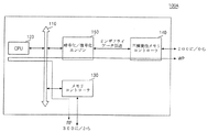
図2は、図1に示したシステムオンチップの一実施形態によるブロック図である。図2を参照すると、図1のSoC100の一実施形態によるSoC100Aは、バス(bus)110、CPU120、メモリコントローラ130、不揮発性メモリコントローラ140、及び暗号化/復号化エンジン150を含む。
FIG. 2 is a block diagram of one embodiment of the system on chip shown in FIG. Referring to FIG. 2, the
CPU120は、バス110に接続され、SoC100Aの全般的な動作を制御する。メモリコントローラ130は、メインメモリ300の動作、例えばリード(read)動作又はライト(write)動作を制御する。メモリコントローラ130は、バス110に接続される。
The
不揮発性メモリコントローラ140は、不揮発性メモリ装置200のデータアクセス動作、例えばリード動作、ライト動作、プログラム(program)動作、又はイレーズ(erase)動作などを制御する。
The
暗号化/復号化エンジン150は、メインメモリ300からメモリコントローラ130とバス110とを介して伝送された平文データを暗号文データに変換、即ち暗号化する。暗号化/復号化エンジン150は、暗号文データを、バス110を経由せずに不揮発性メモリコントローラ140に直接、例えばオンザフライ(on−the−fly)で伝送する。
The encryption /
暗号化/復号化エンジン150は、不揮発性メモリコントローラ140から出力された暗号文データを、バス110を経由せずに直接、例えばオンザフライで受信する。暗号化/復号化エンジン150は、暗号文データを平文データに変換、例えば復号化する。
The encryption /
暗号化/復号化エンジン150の暗号化過程又は復号化過程には、暗号キーが使われる。暗号化/復号化エンジン150は、暗号キーを保存するための記憶媒体(図示せず)を含む。他の実施形態として、暗号キーは、セキュリティモード(Secure Mode)でのみ記憶媒体にアクセス可能になるように設定し得る。セキュリティモードは、図3を参照して詳しく説明する。
An encryption key is used in the encryption process or decryption process of the encryption /
暗号化/復号化エンジン150は、データを所定サイズ、例えば64ビット、128ビット、又は256ビットのブロック(block)単位で暗号化又は復号化する。この場合、暗号化又は復号化のための暗号キーとアルゴリズム(algorithm)は、ブロック単位で適用可能である。
The encryption /
暗号化アルゴリズムは、DES(Data Encryption Standard)アルゴリズム又はAES(Advanced EncryptionStandard)アルゴリズムであり得るが、これに限定されるものではない。実施形態として、暗号化/復号化エンジン150がデータをブロック単位で変換、例えば暗号化又は復号化する方法を決定する暗号モードは、ECB(Electronic Code Book)モード、CBC(Cipher Block Chaining)モード、PCBC(Propagating Cipher Block Chaining)モード、又はCFB(Cipher Feed Back)モードであり得るが、本発明の範囲はこれに限定されるものではない。
The encryption algorithm may be a DES (Data Encryption Standard) algorithm or an AES (Advanced Encryption Standard) algorithm, but is not limited thereto. As an embodiment, an encryption mode in which the encryption /
データが、不揮発性メモリ装置200にライトされる時のライトデータパス(write data path:WP)を説明すると、メインメモリ300から出力された平文データがメモリコントローラ130とバス110とを介してCPU120に伝送された後、平文データは、CPU120からバス110を介して暗号化/復号化エンジン150に伝送される。即ち、CPU120の制御によって、平文データは、暗号化/復号化エンジン150に伝送される。
A write data path (WP) when data is written to the
暗号化/復号化エンジン150は、暗号キーを用いて平文データを暗号文データに変換する。暗号文データは、不揮発性メモリコントローラ140を介して不揮発性メモリ装置200に伝送される。
The encryption /
データが、不揮発性メモリ装置200からリードされる時のリードデータパス(read data path:RP)を説明すると、不揮発性メモリ装置200から出力された暗号文データは、不揮発性メモリコントローラ140を介して暗号化/復号化エンジン150に直接伝送される。
A read data path (RP) when data is read from the
暗号化/復号化エンジン150は、暗号キーを用いて暗号文データを平文データに変換する。平文データがバス110を介してCPU120に伝送された後、平文データは、CPU120からバス110とメモリコントローラ130とを介してメインメモリ300に伝送される。即ち、CPU120の制御によって、平文データは、バス110とメモリコントローラ130とを介してメインメモリ300に伝送される。
The encryption /
図3は、図2に示した暗号化/復号化エンジンに暗号キーを入力するセキュリティモードを説明するための概念図である。図2及び図3を参照すると、オペレーティングシステム(Operating System:OS)は、ハードウェアを管理し、応用プログラム(Application Program)を実行させるために、ハードウェアに設けられる。 FIG. 3 is a conceptual diagram for explaining a security mode in which an encryption key is input to the encryption / decryption engine shown in FIG. Referring to FIGS. 2 and 3, an operating system (OS) is provided in the hardware to manage the hardware and execute an application program (Application Program).
セキュリティ(Secure)OSは、セキュリティが要求されるセキュリティ応用プログラム(Secure Application Program)を実行させるために、一般的なオペレーティングシステム(OS)とは別個にハードウェアに設けられる。実施形態として、セキュリティOSは、所定時間内に実行が完了しなければならない応用プログラム、例えば、セキュリティ応用プログラムを実行させるために、リアルタイムオペレーティングシステム(Real Time Operating System:RTOS)として具現可能である。 A security OS is provided in hardware separately from a general operating system (OS) in order to execute a security application program (Secure Application Program) that requires security. As an embodiment, the security OS can be embodied as a real time operating system (RTOS) in order to execute an application program that must be executed within a predetermined time, for example, a security application program.
非セキュリティモードとは、オペレーティングシステム(OS)によって応用プログラムが実行される場合を意味し、セキュリティモードとは、セキュリティOSによってセキュリティ応用プログラムが実行される場合を意味する。セキュリティモードでセキュリティ応用プログラムが実行されることによって、CPU120は、暗号化/復号化エンジン150に暗号キーを入力するか、或いは暗号化/復号化エンジン150の内部又は外部に保存されている暗号キーにアクセスする。実施形態として、セキュリティモードでセキュリティ応用プログラムが実行されることによって、暗号キーは、変更又は再設定され得る。
The non-security mode means a case where the application program is executed by the operating system (OS), and the security mode means a case where the security application program is executed by the security OS. When the security application program is executed in the security mode, the
図4は、図1に示したシステムオンチップの他の実施形態によるブロック図である。図1〜図4を参照すると、図1のSoC100の他の実施形態によるSoC100Bは、バス110、CPU120、メモリコントローラ130、不揮発性メモリコントローラ140、暗号化/復号化エンジン150、及び第1OTPメモリ(One−Time Programmable Memory)160を含む。第1OTPメモリ160は、暗号化/復号化エンジン150の暗号化過程又は復号化過程で使われる暗号キーを保存する。実施形態として、第1OTPメモリ160は、ヒューズ(fuse)、アンチヒューズ(anti−fuse)、又は電子ヒューズとして具現可能である。
FIG. 4 is a block diagram of another embodiment of the system on chip shown in FIG. 1-4, the
図4のSoC100Bは、図2のSoC100Aとは異なって、セキュリティモードでセキュリティ応用プログラムが実行されても、CPU120は、第1OTPメモリ160に保存された暗号キーにアクセス、例えばリード、ライト、又はイレーズできないように具現される。
Unlike the
データの暗号化又は復号化に使われる暗号キーが、第1OTPメモリ160から暗号化/復号化エンジン150に供給されることを除けば、図4のSoC100BのライトデータパスWP及びリードデータパスRPのそれぞれは、図2のSoC100AのライトデータパスWP及びリードデータパスRPのそれぞれと実質的に同一である。
Except that the encryption key used for data encryption or decryption is supplied from the
図5は、図1に示したシステムオンチップの更に他の実施形態によるブロック図である。図1及び図5を参照すると、図1のSoC100の更に他の実施形態によるSoC100Cは、バス110、CPU120、メモリコントローラ130、不揮発性メモリコントローラ140、暗号化/復号化エンジン150、第1OTPメモリ160、及びDMAユニット(Direct Memory Access Unit)170を含む。
FIG. 5 is a block diagram of still another embodiment of the system on chip shown in FIG. Referring to FIGS. 1 and 5, the
DMAユニット170は、CPU120を介さずに必要な構成(例えば、130、140、又は150)を介してメインメモリ300又は不揮発性メモリ装置200にアクセスすることができる。この際、DMAユニット170は、バス110に接続される。
The
不揮発性メモリ装置200が、データをライトする時のライトデータパスWPを説明すると、メインメモリ300から出力された平文データは、メモリコントローラ130とバス110とを介してDMAユニット170に伝送される。平文データは、DMAユニット170からバス110を介して暗号化/復号化エンジン150に伝送される。
The write data path WP when the
暗号化/復号化エンジン150は、平文データを暗号文データに変換する。暗号化/復号化エンジン150から出力された暗号文データは、直接不揮発性メモリコントローラ140に伝送された後、不揮発性メモリ装置200に伝送される。即ち、暗号化/復号化エンジン150は、暗号文データを不揮発性メモリコントローラ140に直接、例えばオンザフライで伝送する。
The encryption /
データが、不揮発性メモリ装置200からリードされる時のリードデータパスRPを説明すると、不揮発性メモリ装置200から出力された暗号文データは、不揮発性メモリコントローラ140を介して暗号化/復号化エンジン150に伝送される。即ち、暗号化/復号化エンジン150は、不揮発性メモリコントローラ140から出力された暗号文データを直接、例えばオンザフライで受信する。
The read data path RP when data is read from the
暗号化/復号化エンジン150は、暗号文データを平文データに変換する。平文データは、バス110を介してDMAユニット170に伝送される。平文データは、DMAユニット170からバス110とメモリコントローラ130とを介してメインメモリ300に伝送される。
The encryption /
図6は、図1に示したシステムオンチップの更に他の実施形態によるブロック図である。図1及び図6を参照すると、図1のSoC100の更に他の実施形態によるSoC100Dは、バス110、CPU120、メモリコントローラ130、不揮発性メモリコントローラ140、暗号化/復号化エンジン150、第1OTPメモリ160、及びDMAユニット170を含む。
FIG. 6 is a block diagram of still another embodiment of the system on chip shown in FIG. 1 and 6, the SoC 100D according to another embodiment of the
DMAユニット170は、バス110と暗号化/復号化エンジン150との間に接続される。データは、DMAユニット170と暗号化/復号化エンジン150との間で、オンザフライで伝送される。
The
不揮発性メモリ装置200が、データをライトする時のライトデータパスWPを説明すると、メインメモリ300から出力された平文データは、メモリコントローラ130、バス110、及びDMAユニット170を介して暗号化/復号化エンジン150に伝送される。
The write data path WP when the
暗号化/復号化エンジン150は、平文データを暗号文データに変換、例えば暗号化する。暗号文データは、不揮発性メモリコントローラ140を介して不揮発性メモリ装置200に伝送される。この際、暗号化/復号化エンジン150は、不揮発性メモリコントローラ140に暗号文データを直接、例えばオンザフライで伝送する。
The encryption /
不揮発性メモリ装置200が、データをリードする時のリードデータパスRPを説明すると、不揮発性メモリ装置200から出力された暗号文データは、不揮発性メモリコントローラ140を介して暗号化/復号化エンジン150に伝送される。この際、暗号化/復号化エンジン150は、不揮発性メモリコントローラ140から暗号文データを直接、例えばオンザフライで受信する。
The read data path RP when the
暗号化/復号化エンジン150は、暗号文データを平文データに変換、例えば復号化する。平文データは、DMAユニット170、バス110、及びメモリコントローラ130を介してメインメモリ300に伝送される。
The encryption /
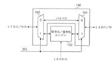
図7は、図1に示したシステムオンチップの更に他の実施形態によるブロック図である。図1、図3、及び図7を参照すると、図1のSoC100の更に他の実施形態によるSoC100Eは、バス110、CPU120、メモリコントローラ130、不揮発性メモリコントローラ140、暗号化/復号化エンジン150、第1OTPメモリ160、DMAユニット170、レジスタ180、及び選択回路190を含む。
FIG. 7 is a block diagram of still another embodiment of the system on chip shown in FIG. Referring to FIGS. 1, 3, and 7, the
レジスタ180は、バス110に接続される。レジスタ180は、選択信号SELを発生する選択信号発生器として作動する。レジスタ180は、CPU120がセキュリティ応用プログラムを実行するか否か、即ちセキュリティモードを指示する指示信号に基づいて選択信号SELを変更する。指示信号は、CPU120から出力される。
The
例えば、セキュリティモードで、指示信号のロジックレベルは、ハイ(high)であり、非セキュリティモードで、指示信号のロジックレベルは、ロー(low)である。選択回路190は、レジスタ180から出力された選択信号SELによってデータパスを選択する。選択回路190の構造と動作は、図8を参照して詳しく説明する。
For example, in the security mode, the logic level of the instruction signal is high, and in the non-security mode, the logic level of the instruction signal is low. The
図8は、図7に示した選択回路及び暗号化/復号化エンジンのブロック図である。図3、図7、及び図8を参照すると、選択回路190は、第1選択器192と第2選択器194とを含む。
FIG. 8 is a block diagram of the selection circuit and the encryption / decryption engine shown in FIG. Referring to FIGS. 3, 7, and 8, the
第1選択器192は、デマルチプレクサとして具現可能であり、第2選択器194は、マルチプレクサとして具現可能である。
The
選択回路190は、選択信号SELのロジックレベルがハイである時、データが暗号化/復号化エンジン150を含むデータパスを選択する。CPU120がセキュリティ応用プログラムを実行する時、即ちセキュリティモードである時、選択回路190は、暗号化/復号化エンジン150を含むデータパスを選択する。しかし、選択回路190は、選択信号SELのロジックレベルがローである時、暗号化/復号化エンジン150を含まないデータパス、即ちバイパスを選択することができる。実施形態として、CPU120が一般応用プログラムを実行する時、即ち非セキュリティモードである時、選択回路190は、暗号化/復号化エンジン150を含まないデータパス、即ちバイパスを選択する。
The
図9は、図1に示したシステムオンチップの更に他の実施形態によるブロック図である。図1、図8、及び図9を参照すると、図1のSoC100の更に他の実施形態によるSoC100Fは、バス110、CPU120、メモリコントローラ130、不揮発性メモリコントローラ140、暗号化/復号化エンジン150、第1OTPメモリ160、DMAユニット170、第2OTPメモリ182、及び選択回路190を含む。
FIG. 9 is a block diagram of still another embodiment of the system on chip shown in FIG. Referring to FIGS. 1, 8, and 9, the
第2OTPメモリ182は、選択信号SELを発生する選択信号発生器として作動する。第2OTPメモリ182は、1つのレベル、例えばハイレベルを有する選択信号SELを発生するようにプログラムされる。この際、選択回路190は、暗号化/復号化エンジン150を含むデータパスのみを選択する。
The
図10は、本発明の一実施形態によるシステムオンチップの動作方法を説明するフローチャートである。図2、図4〜図7、図9、及び図10を参照すると、暗号化/復号化エンジン150は、暗号キーを用いて平文データを暗号文データに変換、即ち暗号化する(ステップS10)。
FIG. 10 is a flowchart illustrating a system-on-chip operating method according to an embodiment of the present invention. Referring to FIG. 2, FIG. 4 to FIG. 7, FIG. 9, and FIG. 10, the encryption /
暗号化/復号化エンジン150は、暗号化データを不揮発性メモリコントローラ140に直接、例えばオンザフライで伝送する(ステップS12)。従って、暗号キーと暗号化データは、SoC100の内部に存在するため、プロービングに強い効果がある。
The encryption /
図11は、本発明の他の実施形態によるシステムオンチップの動作方法を説明するフローチャートである。図5〜図7、図9、及び図11を参照すると、暗号化/復号化エンジン150は、平文データをDMAユニット170から受信する(ステップS20)。暗号化/復号化エンジン150は、平文データをDMAユニット170から直接、例えばオンザフライで受信する。
FIG. 11 is a flowchart illustrating a system-on-chip operating method according to another embodiment of the present invention. 5 to 7, 9, and 11, the encryption /
図12は、本発明の更に他の実施形態によるシステムオンチップの動作方法を説明するフローチャートである。図2、図4〜図7、図9、及び図12を参照すると、暗号化/復号化エンジン150は、不揮発性メモリコントローラ140から暗号文データを直接、例えばオンザフライで受信する(ステップS30)。暗号化/復号化エンジン150は、暗号文データを平文データに復号化する(ステップS32)。
FIG. 12 is a flowchart illustrating a method of operating a system on chip according to still another embodiment of the present invention. Referring to FIG. 2, FIG. 4 to FIG. 7, FIG. 9, and FIG. 12, the encryption /
図13は、本発明の更に他の実施形態によるシステムオンチップの動作方法を説明するフローチャートである。図5〜図7、図9、及び図13を参照すると、暗号化/復号化エンジン150は、平文データをDMAユニット170に伝送する(ステップS34)。暗号化/復号化エンジン150は、平文データをDMAユニット170に直接、例えばオンザフライで伝送する。
FIG. 13 is a flowchart illustrating a method of operating a system on chip according to still another embodiment of the present invention. 5 to 7, 9, and 13, the encryption /
図14は、図1に示したシステムを含むデータ処理装置の一実施形態によるブロック図である。図1及び図14を参照すると、データ処理装置400は、PC又はデータサーバとして具現可能である。
FIG. 14 is a block diagram of an embodiment of a data processing apparatus including the system shown in FIG. Referring to FIGS. 1 and 14, the
データ処理装置400は、プロセッサ100a、保存装置200a、メモリ300a、パワーソース410、入出力ポート420、拡張カード430、ネットワーク装置440、及びディスプレイ450を含む。実施形態として、データ処理装置400は、カメラモジュール460を更に含み得る。
The
プロセッサ100aは、図1に示したSoC100を意味する。プロセッサ100aは、マルチコア(Multi−Core)プロセッサであり得る。実施形態として、プロセッサ100aは、図1に示したSoC100を含む。プロセッサ100aは、構成要素(200a、300a、及び410〜460)のうちの少なくとも1つの動作を制御する。
The
保存装置200aは、図1に示した不揮発性メモリ装置200を意味する。保存装置200aは、ハードディスクドライブ(Hard Disk Drive)又はSSD(Solid State Drive)として具現可能である。
The
メモリ300aは、図1に示したメインメモリ300を意味する。メモリ300aは、揮発性メモリ又は不揮発性メモリとして具現可能である。メモリ300aに対するデータアクセス動作、例えばリード動作、ライト動作(又は、プログラム動作)、又はイレーズ動作を制御するメモリコントローラ(図2の140)は、プロセッサ100に集積又は内蔵され得る。
The
パワーソース410は、構成要素(100a、200a、300a及び420〜460)のうちの少なくとも1つに動作電圧を供給する。
The
入出力ポート420は、保存装置200aにデータを伝送するか、保存装置200aから出力されたデータを外部装置に伝送するポートを意味する。例えば、入出力ポート420は、コンピュータマウスのようなポインティング装置(pointing device)を接続するためのポート、プリンターを接続するためのポート、又はUSB(Universal Serial Bus)ドライブを接続するためのポートである。
The input /
拡張カード430は、SD(Secure Digital)カード又はMMC(MultiMedia Card)として具現可能である。実施形態として、拡張カード430は、SIM(Subscriber Identification Module)カード又はUSIM(Universal Subscriber Identity Module)カードであり得る。
The
ネットワーク装置440は、保存装置200aを有線ネットワーク又は無線ネットワークに接続させる装置を意味する。
The
ディスプレイ450は、保存装置200a、メモリ300a、入出力ポート420、拡張カード430、又はネットワーク装置440から出力されたデータを表示する。カメラモジュール460は、光学イメージを電気的なイメージに変換するモジュールを意味する。従って、カメラモジュール460から出力された電気的なイメージは、保存装置200a、メモリ300a、又は拡張カード430に保存される。また、カメラモジュール460から出力された電気的なイメージは、ディスプレイ450を通じて表示される。
The
図15は、図1に示したシステムを含むデータ処理装置の他の実施形態によるブロック図である。図1及び図15を参照すると、データ処理装置500は、ラップトップ(laptop)コンピュータとして具現可能である。
FIG. 15 is a block diagram of another embodiment of a data processing apparatus including the system shown in FIG. Referring to FIGS. 1 and 15, the
図16は、図1に示したシステムを含むデータ処理装置の更に他の実施形態によるブロック図である。図1及び図16を参照すると、データ処理装置600は、携帯用装置として具現可能である。携帯用装置600は、携帯電話、スマートフォン、タブレットPC、PDA、EDA、デジタルスチルカメラ、デジタルビデオカメラ、PMP、PDN、携帯用ゲームコンソール、又は電子ブックとして具現可能である。
FIG. 16 is a block diagram according to still another embodiment of the data processing apparatus including the system shown in FIG. 1 and 16, the
図17は、図1に示したシステムオンチップを含むシステムインパッケージ及び不揮発性メモリ装置のブロック図であり、図18は、図1に示したシステムオンチップを含むシステムインパッケージの他の実施形態によるブロック図である。図1及び図17を参照すると、SoC100及びメインメモリ300は、システムインパッケージ(SiP)700にパッケージングされる。図1及び図18を参照すると、SoC100、不揮発性メモリ装置200、及びメインメモリ300は、SiP700′にパッケージングされる。
17 is a block diagram of a system-in-package and a non-volatile memory device including the system-on-chip shown in FIG. 1, and FIG. 18 is another embodiment of the system-in-package including the system-on-chip shown in FIG. FIG. Referring to FIGS. 1 and 17, the
以上、本発明の実施形態について図面を参照しながら詳細に説明したが、本発明は、上述の実施形態に限定されるものではなく、本発明の技術的範囲から逸脱しない範囲内で多様に変更実施することが可能である。 As mentioned above, although embodiment of this invention was described in detail, referring drawings, this invention is not limited to the above-mentioned embodiment, In the range which does not deviate from the technical scope of this invention, it changes variously. It is possible to implement.
10 システム
100、100A、100B、100C、100D、100E、100F システムオンチップ(SoC)
100a プロセッサ
110 バス
120 CPU
130 メモリコントローラ
140 不揮発性メモリコントローラ
150 暗号化/復号化エンジン
160 第1OTPメモリ
170 DMAユニット
180 レジスタ
182 第2OTPメモリ
190 選択回路
192 第1選択器
194 第2選択器
200 不揮発性メモリ装置
200a 保存装置
300 メインメモリ
300a メモリ
400、500、600 データ処理装置
410、510、610 パワーソース
420、520、620 入出力ポート
430、530、630 拡張カード
440、540、640 ネットワーク装置
450、550、650 ディスプレイ
460、560、660 カメラモジュール
700、700′ システムインパッケージ(SiP)
10
130
Claims (20)
前記SoCに含まれるエンジンが、前記SoCに含まれるデータバスを介して平文データを受信する段階と、
前記エンジンが、前記SoCに含まれるCPUによってセキュリティモードで入力された暗号キーを用いて前記平文データを暗号文データに変換する段階と、
前記エンジンが、前記暗号文データを前記SoCに含まれるメモリコントローラに前記データバスを介すること無く、直接伝送する段階と、を有し、
前記メモリコントローラは、不揮発性メモリの動作を制御することを特徴とするシステムオンチップの動作方法。 A system-on-chip (SoC) operation method,
An engine included in the SoC receives plaintext data via a data bus included in the SoC;
The engine includes a step of converting the plaintext data into ciphertext data using the encryption key entered by the security mode by the CPU included in the SoC,
Said engine, said without the encrypted data via the data bus to the memory controller included in the SoC, a and transmitting directly to,
A system-on-chip operation method, wherein the memory controller controls an operation of a nonvolatile memory.
前記SoCに含まれるエンジンが、前記SoCに含まれるメモリコントローラから暗号文データを直接受信する段階と、
前記エンジンが、前記SoCに含まれるCPUによってセキュリティモードで前記エンジンに入力された暗号キーを用いて前記暗号文データを平文データに変換する段階と、を有し、
前記メモリコントローラは、不揮発性メモリの動作を制御することを特徴とするシステムオンチップの動作方法。 A system-on-chip (SoC) operation method,
The method comprising the engine included in the SoC receives directly the encrypted data from the memory controller included in the SoC,
The engine has a, and converting the ciphertext data into plaintext data using the encryption key entered by the security mode to the engine by a CPU included in the SoC,
A system-on-chip operation method, wherein the memory controller controls an operation of a nonvolatile memory.
CPUと、
前記CPUによってセキュリティモードで入力された暗号キーを用いて、第1平文データを第1暗号文データに暗号化し、第2暗号文データを第2平文データに復号化する暗号化/復号化エンジンと、
前記暗号化/復号化エンジンに直接接続され、前記第1暗号文データを不揮発性メモリに伝送し、前記不揮発性メモリから前記第2暗号文データを受信するメモリコントローラと、を有し、
前記暗号化/復号化エンジンと前記メモリコントローラとは直接接続され、前記暗号化/復号化エンジンと前記メモリコントローラとの間にはいかなる装置も接続されないことを特徴とするシステムオンチップ。 System on chip (SoC),
CPU,
An encryption / decryption engine that encrypts the first plaintext data into the first ciphertext data and decrypts the second ciphertext data into the second plaintext data using the encryption key input in the security mode by the CPU ; ,
Which is connected directly to the encryption / decryption engine, transmitting the first encrypted data into the nonvolatile memory, have a, a memory controller for receiving the second ciphertext data from the nonvolatile memory,
The system on chip, wherein the encryption / decryption engine and the memory controller are directly connected, and no device is connected between the encryption / decryption engine and the memory controller .
前記SoCの制御によって、不揮発性メモリとデータを通信する装置と、を備えることを特徴とするシステムインパッケージ。 A system on chip (SoC) according to claim 5;
A system-in-package comprising: a device that communicates data with a nonvolatile memory under the control of the SoC.
不揮発性メモリと、
前記SoCの制御によって、前記不揮発性メモリとデータを通信する装置と、を備えることを特徴とするシステムインパッケージ。 A system on chip (SoC) according to claim 5;
Non-volatile memory;
A system-in-package comprising: a device that communicates data with the nonvolatile memory under the control of the SoC.
CPUと、
外部の揮発性メモリから平文データを受信する揮発性メモリコントローラと、
不揮発性メモリコントローラに直接接続され、前記揮発性メモリコントローラから送信された前記平文データを、前記CPUによってセキュリティモードで入力された暗号キーを用いて暗号文データに暗号化する暗号化エンジンと、
前記CPU及び前記揮発性メモリコントローラに接続されたデータバスと、
不揮発性メモリを制御し、前記平文データを送信するために用いられる前記データバスを介すること無く、前記暗号文データを前記暗号化エンジンから直接受信する不揮発性メモリコントローラと、を有し、
前記SoCは、前記SoCの外部にある装置と前記不揮発性メモリとの間のデータの伝送を制御し、
前記不揮発性メモリコントローラ及び前記暗号化エンジンは、前記データを伝送するための第1データパスに該当し、
前記暗号化エンジンと前記不揮発性メモリコントローラとは直接接続され、前記暗号化エンジンと前記不揮発性メモリコントローラとの間にはいかなる装置も接続されないことを特徴とするシステムオンチップ。 System on chip (SoC),
CPU,
A volatile memory controller to receive a plaintext data from the external volatile memory,
An encryption engine that is directly connected to a non-volatile memory controller and that encrypts the plaintext data transmitted from the volatile memory controller into ciphertext data using an encryption key input in a security mode by the CPU ;
A data bus connected to the CPU and the volatile memory controller;
A nonvolatile memory controller that controls the nonvolatile memory and receives the ciphertext data directly from the encryption engine without going through the data bus used to transmit the plaintext data ,
The SoC controls transmission of data between a device outside the SoC and the nonvolatile memory;
The nonvolatile memory controller and the encryption engine correspond to a first data path for transmitting the data ,
The system on chip, wherein the encryption engine and the non-volatile memory controller are directly connected, and no device is connected between the encryption engine and the non-volatile memory controller .
前記暗号化エンジンは、前記OTPメモリに保存された暗号キーを用いて、前記データを暗号化することを特徴とする請求項11に記載のシステムオンチップ。 Further comprising a one-time programmable (OTP) memory for storing the cryptographic key;
The encryption engine using the encryption key stored in the OTP memory, system-on-chip according to claim 11, characterized by encrypting the data.
CPUと、
前記CPUに接続されたデータバスと、
前記データバスに平文データを出力するメインメモリコントローラと、
前記データバスから受信した前記平文データを、前記CPUによってセキュリティモードで入力された暗号キーを用いて暗号文データに暗号化するエンジンと、
前記データバスを介すること無く、前記暗号文データを前記エンジンから直接受信する不揮発性メモリコントローラと、
前記エンジンをバイパスして前記データバスを前記不揮発性メモリコントローラに接続させる第1電気的経路と、
前記エンジンを介して前記データバスを前記不揮発性メモリコントローラに接続させる第2電気的経路と、を有し、
前記SoCは、非セキュリティモードで、前記平文データを前記データバスから前記不揮発性メモリコントローラに伝送するために前記第1電気的経路のみを活性化させ、
前記SoCは、セキュリティモードで、前記平文データを前記エンジンに伝送し、前記エンジンから受信した前記暗号文データを前記不揮発性メモリコントローラに伝送するために前記第2電気的経路のみを活性化させ、
前記エンジンと前記不揮発性メモリコントローラとは直接接続され、前記エンジンと前記不揮発性メモリコントローラとの間にはいかなる装置も接続されないことを特徴とするシステムオンチップ。 System on chip (SoC),
CPU,
A data bus connected to the CPU ;
A main memory controller for outputting plaintext data to the data bus;
An engine that encrypts the plaintext data received from the data bus into ciphertext data using an encryption key input in a security mode by the CPU ;
A non-volatile memory controller that directly receives the ciphertext data from the engine without going through the data bus ;
A first electrical path that bypasses the engine and connects the data bus to the non-volatile memory controller;
A second electrical path connecting the data bus to the non-volatile memory controller through the engine,
The SoC activates only the first electrical path to transmit the plaintext data from the data bus to the nonvolatile memory controller in a non-security mode,
The SoC is the security mode, the transmit plaintext data to the engine, to activate only the second electrical path for transmitting the ciphertext data received to the non-volatile memory controller from said engine,
The system and the nonvolatile memory controller are directly connected, and no device is connected between the engine and the nonvolatile memory controller .
The system on chip according to claim 17, wherein the engine decrypts ciphertext data received from the nonvolatile memory controller via the second electrical path.
Applications Claiming Priority (2)
| Application Number | Priority Date | Filing Date | Title |
|---|---|---|---|
| KR10-2012-0047743 | 2012-05-04 | ||
| KR1020120047743A KR101975027B1 (en) | 2012-05-04 | 2012-05-04 | System on chip, operation method thereof, and devices having the same |
Publications (3)
| Publication Number | Publication Date |
|---|---|
| JP2013236376A JP2013236376A (en) | 2013-11-21 |
| JP2013236376A5 JP2013236376A5 (en) | 2016-05-12 |
| JP6239259B2 true JP6239259B2 (en) | 2017-11-29 |
Family
ID=49384556
Family Applications (1)
| Application Number | Title | Priority Date | Filing Date |
|---|---|---|---|
| JP2013097518A Active JP6239259B2 (en) | 2012-05-04 | 2013-05-07 | System on chip, operation method thereof, and system in package including the same |
Country Status (5)
| Country | Link |
|---|---|
| US (2) | US20130297948A1 (en) |
| JP (1) | JP6239259B2 (en) |
| KR (1) | KR101975027B1 (en) |
| CN (1) | CN103383668B (en) |
| DE (1) | DE102013104167A1 (en) |
Families Citing this family (78)
| Publication number | Priority date | Publication date | Assignee | Title |
|---|---|---|---|---|
| ES2556271T3 (en) * | 2008-08-22 | 2016-01-14 | Qualcomm Incorporated | Procedure and apparatus for transmitting and receiving protected data and unprotected data |
| US20140244513A1 (en) * | 2013-02-22 | 2014-08-28 | Miguel Ballesteros | Data protection in near field communications (nfc) transactions |
| US9607178B2 (en) * | 2014-03-20 | 2017-03-28 | Qualcomm Incorporated | Protection against key tampering |
| CN103941119B (en) * | 2014-03-27 | 2016-09-07 | 北京汇德信科技有限公司 | A kind of multifunction programable signal generation parameter test system |
| KR102157668B1 (en) * | 2014-04-03 | 2020-09-22 | 에스케이하이닉스 주식회사 | Memory controller communicating with host, and operating method thereof, and computing system including the same |
| US10169618B2 (en) | 2014-06-20 | 2019-01-01 | Cypress Semiconductor Corporation | Encryption method for execute-in-place memories |
| US10192062B2 (en) * | 2014-06-20 | 2019-01-29 | Cypress Semiconductor Corporation | Encryption for XIP and MMIO external memories |
| US10691838B2 (en) | 2014-06-20 | 2020-06-23 | Cypress Semiconductor Corporation | Encryption for XIP and MMIO external memories |
| US9621549B2 (en) * | 2014-07-25 | 2017-04-11 | Qualcomm Incorporated | Integrated circuit for determining whether data stored in external nonvolative memory is valid |
| US9298647B2 (en) | 2014-08-25 | 2016-03-29 | HGST Netherlands B.V. | Method and apparatus to generate zero content over garbage data when encryption parameters are changed |
| KR102208072B1 (en) * | 2014-09-01 | 2021-01-27 | 삼성전자주식회사 | Data processing system |
| US9660806B2 (en) * | 2014-12-30 | 2017-05-23 | International Business Machines Corporation | Carbon nanotube array for cryptographic key generation and protection |
| US9734117B2 (en) * | 2015-01-26 | 2017-08-15 | Western Digital Technologies, Inc. | Data storage device and method for integrated bridge firmware to be retrieved from a storage system on chip (SOC) |
| US11023453B2 (en) * | 2015-01-29 | 2021-06-01 | Hewlett Packard Enterprise Development Lp | Hash index |
| WO2016122547A1 (en) * | 2015-01-29 | 2016-08-04 | Hewlett Packard Enterprise Development Lp | Foster twin data structure |
| KR102347827B1 (en) * | 2015-02-12 | 2022-01-07 | 삼성전자주식회사 | Apparatus and method for secure message transmission |
| US9560737B2 (en) | 2015-03-04 | 2017-01-31 | International Business Machines Corporation | Electronic package with heat transfer element(s) |
| CN106155568B (en) * | 2015-04-03 | 2019-03-01 | 华为技术有限公司 | A kind of method and terminal of partition holding |
| US9779262B2 (en) * | 2015-04-20 | 2017-10-03 | Qualcomm Incorporated | Apparatus and method to decrypt file segments in parallel |
| US10426037B2 (en) | 2015-07-15 | 2019-09-24 | International Business Machines Corporation | Circuitized structure with 3-dimensional configuration |
| CN106407829A (en) * | 2015-07-30 | 2017-02-15 | 宇龙计算机通信科技(深圳)有限公司 | Fingerprint recognition-based file encryption method and device and mobile terminal |
| US9591776B1 (en) | 2015-09-25 | 2017-03-07 | International Business Machines Corporation | Enclosure with inner tamper-respondent sensor(s) |
| US10172239B2 (en) | 2015-09-25 | 2019-01-01 | International Business Machines Corporation | Tamper-respondent sensors with formed flexible layer(s) |
| US9924591B2 (en) | 2015-09-25 | 2018-03-20 | International Business Machines Corporation | Tamper-respondent assemblies |
| US10098235B2 (en) | 2015-09-25 | 2018-10-09 | International Business Machines Corporation | Tamper-respondent assemblies with region(s) of increased susceptibility to damage |
| US9578764B1 (en) | 2015-09-25 | 2017-02-21 | International Business Machines Corporation | Enclosure with inner tamper-respondent sensor(s) and physical security element(s) |
| US9894749B2 (en) | 2015-09-25 | 2018-02-13 | International Business Machines Corporation | Tamper-respondent assemblies with bond protection |
| US9911012B2 (en) | 2015-09-25 | 2018-03-06 | International Business Machines Corporation | Overlapping, discrete tamper-respondent sensors |
| US10175064B2 (en) | 2015-09-25 | 2019-01-08 | International Business Machines Corporation | Circuit boards and electronic packages with embedded tamper-respondent sensor |
| US10671762B2 (en) | 2015-09-29 | 2020-06-02 | Apple Inc. | Unified addressable memory |
| KR102458351B1 (en) * | 2015-10-02 | 2022-10-26 | 삼성전자주식회사 | Authentication apparatus based on public key cryptosystem, mobile device having the same and authentication method thereof |
| US10143090B2 (en) | 2015-10-19 | 2018-11-27 | International Business Machines Corporation | Circuit layouts of tamper-respondent sensors |
| US9978231B2 (en) | 2015-10-21 | 2018-05-22 | International Business Machines Corporation | Tamper-respondent assembly with protective wrap(s) over tamper-respondent sensor(s) |
| CN105426793B (en) * | 2015-11-17 | 2018-02-06 | 无锡江南计算技术研究所 | A kind of multi bri device controller encryption and decryption dispatch control method |
| US9913389B2 (en) | 2015-12-01 | 2018-03-06 | International Business Corporation Corporation | Tamper-respondent assembly with vent structure |
| US10327343B2 (en) | 2015-12-09 | 2019-06-18 | International Business Machines Corporation | Applying pressure to adhesive using CTE mismatch between components |
| US9555606B1 (en) | 2015-12-09 | 2017-01-31 | International Business Machines Corporation | Applying pressure to adhesive using CTE mismatch between components |
| US10225247B2 (en) | 2015-12-14 | 2019-03-05 | Intel Corporation | Bidirectional cryptographic IO for data streams |
| US9554477B1 (en) | 2015-12-18 | 2017-01-24 | International Business Machines Corporation | Tamper-respondent assemblies with enclosure-to-board protection |
| US10382410B2 (en) * | 2016-01-12 | 2019-08-13 | Advanced Micro Devices, Inc. | Memory operation encryption |
| WO2017127084A1 (en) | 2016-01-21 | 2017-07-27 | Hewlett-Packard Development Company, L.P. | Data cryptography engine |
| US9916744B2 (en) | 2016-02-25 | 2018-03-13 | International Business Machines Corporation | Multi-layer stack with embedded tamper-detect protection |
| US9904811B2 (en) | 2016-04-27 | 2018-02-27 | International Business Machines Corporation | Tamper-proof electronic packages with two-phase dielectric fluid |
| DE102016116152A1 (en) * | 2016-04-30 | 2017-11-02 | Krohne Messtechnik Gmbh | Electrical device with a functional device |
| US9913370B2 (en) | 2016-05-13 | 2018-03-06 | International Business Machines Corporation | Tamper-proof electronic packages formed with stressed glass |
| US9881880B2 (en) | 2016-05-13 | 2018-01-30 | International Business Machines Corporation | Tamper-proof electronic packages with stressed glass component substrate(s) |
| US10762030B2 (en) * | 2016-05-25 | 2020-09-01 | Samsung Electronics Co., Ltd. | Storage system, method, and apparatus for fast IO on PCIE devices |
| US9858776B1 (en) | 2016-06-28 | 2018-01-02 | International Business Machines Corporation | Tamper-respondent assembly with nonlinearity monitoring |
| US10261919B2 (en) * | 2016-07-08 | 2019-04-16 | Hewlett Packard Enterprise Development Lp | Selective memory encryption |
| US10321589B2 (en) | 2016-09-19 | 2019-06-11 | International Business Machines Corporation | Tamper-respondent assembly with sensor connection adapter |
| US10271424B2 (en) | 2016-09-26 | 2019-04-23 | International Business Machines Corporation | Tamper-respondent assemblies with in situ vent structure(s) |
| US10299372B2 (en) | 2016-09-26 | 2019-05-21 | International Business Machines Corporation | Vented tamper-respondent assemblies |
| US9999124B2 (en) | 2016-11-02 | 2018-06-12 | International Business Machines Corporation | Tamper-respondent assemblies with trace regions of increased susceptibility to breaking |
| US10326587B2 (en) * | 2016-12-28 | 2019-06-18 | Intel Corporation | Ultra-lightweight cryptography accelerator system |
| US10896267B2 (en) * | 2017-01-31 | 2021-01-19 | Hewlett Packard Enterprise Development Lp | Input/output data encryption |
| US10327329B2 (en) | 2017-02-13 | 2019-06-18 | International Business Machines Corporation | Tamper-respondent assembly with flexible tamper-detect sensor(s) overlying in-situ-formed tamper-detect sensor |
| KR20190075363A (en) * | 2017-12-21 | 2019-07-01 | 삼성전자주식회사 | Semiconductor memory device, memory system and memory module including the same |
| US10715321B2 (en) | 2017-12-22 | 2020-07-14 | Micron Technology, Inc. | Physical unclonable function using message authentication code |
| CN108197504B (en) * | 2017-12-28 | 2022-01-11 | 湖南国科微电子股份有限公司 | Controllable data encryption and decryption system and method |
| US10906506B2 (en) | 2017-12-28 | 2021-02-02 | Micron Technology, Inc. | Security of user data stored in shared vehicles |
| US10924277B2 (en) * | 2018-01-25 | 2021-02-16 | Micron Technology, Inc. | Certifying authenticity of stored code and code updates |
| US10306753B1 (en) | 2018-02-22 | 2019-05-28 | International Business Machines Corporation | Enclosure-to-board interface with tamper-detect circuit(s) |
| US11122682B2 (en) | 2018-04-04 | 2021-09-14 | International Business Machines Corporation | Tamper-respondent sensors with liquid crystal polymer layers |
| US10778661B2 (en) | 2018-04-27 | 2020-09-15 | Micron Technology, Inc. | Secure distribution of secret key using a monotonic counter |
| WO2020034118A1 (en) * | 2018-08-15 | 2020-02-20 | 华为技术有限公司 | Secure data transfer apparatus, system and method |
| US10936459B2 (en) * | 2018-12-07 | 2021-03-02 | Microsoft Technology Licensing, Llc | Flexible microcontroller support for device testing and manufacturing |
| KR102621645B1 (en) | 2019-03-12 | 2024-01-05 | 삼성전자주식회사 | Electronic device having secure integrated circuit |
| CN111775698B (en) * | 2019-04-04 | 2021-11-16 | 北京新能源汽车股份有限公司 | Vehicle mileage information processing method and device and automobile |
| KR20200129776A (en) | 2019-05-10 | 2020-11-18 | 삼성전자주식회사 | Method of operating memory system with replay attack countermeasure and memory system performing the same |
| CN112115094A (en) * | 2019-06-21 | 2020-12-22 | 珠海市一微半导体有限公司 | Processor chip and data storage method and data reading method thereof |
| CN110275845B (en) * | 2019-06-29 | 2021-11-19 | 江苏芯盛智能科技有限公司 | Memory control method and device and electronic equipment |
| CN110443078B (en) * | 2019-07-19 | 2021-05-28 | 南京芯驰半导体科技有限公司 | Security storage system based on privilege hierarchy |
| KR20210016764A (en) * | 2019-08-05 | 2021-02-17 | 삼성전자주식회사 | System on chip |
| EP3877884A1 (en) * | 2019-08-29 | 2021-09-15 | Google LLC | Securing external data storage for a secure element integrated on a system-on-chip |
| TWI748570B (en) * | 2020-07-22 | 2021-12-01 | 瑞昱半導體股份有限公司 | Data processing device |
| US11768963B2 (en) * | 2021-01-22 | 2023-09-26 | Nxp Usa, Inc. | System and method for validating trust provisioning operation on system-on-chip |
| CN113312000B (en) * | 2021-06-04 | 2023-04-28 | 河北光兴半导体技术有限公司 | Hard disk and storage system |
| CN113312307A (en) * | 2021-06-25 | 2021-08-27 | 展讯通信(上海)有限公司 | System on chip, data processing method thereof and central processing unit |
Family Cites Families (30)
| Publication number | Priority date | Publication date | Assignee | Title |
|---|---|---|---|---|
| US20080192928A1 (en) * | 2000-01-06 | 2008-08-14 | Super Talent Electronics, Inc. | Portable Electronic Storage Devices with Hardware Security Based on Advanced Encryption Standard |
| JP2003198531A (en) * | 2001-12-27 | 2003-07-11 | Denso Corp | Common key cipher communication method and device |
| EP1355268B1 (en) | 2002-02-28 | 2006-04-05 | Matsushita Electric Industrial Co., Ltd. | Memory card |
| US7941662B2 (en) * | 2002-05-31 | 2011-05-10 | Broadcom Corporation | Data transfer efficiency in a cryptography accelerator system |
| KR20050002103A (en) | 2003-06-30 | 2005-01-07 | (주)파인칩스 | Portable storing apparatus having encryption processor |
| US8954751B2 (en) * | 2004-10-08 | 2015-02-10 | International Business Machines Corporation | Secure memory control parameters in table look aside buffer data fields and support memory array |
| US8332653B2 (en) * | 2004-10-22 | 2012-12-11 | Broadcom Corporation | Secure processing environment |
| US7457985B2 (en) | 2005-09-09 | 2008-11-25 | International Business Machines Corporation | Method to detect errors in computer systems by using state tracking |
| US7934049B2 (en) | 2005-09-14 | 2011-04-26 | Sandisk Corporation | Methods used in a secure yet flexible system architecture for secure devices with flash mass storage memory |
| US20100191959A1 (en) * | 2005-09-23 | 2010-07-29 | Space Micro Inc. | Secure microprocessor and method |
| US20070074046A1 (en) * | 2005-09-23 | 2007-03-29 | Czajkowski David R | Secure microprocessor and method |
| US7835518B2 (en) | 2006-04-03 | 2010-11-16 | Sandisk Corporation | System and method for write failure recovery |
| US20100077230A1 (en) | 2006-12-15 | 2010-03-25 | Michael Chambers | Protecting a programmable memory against unauthorized modification |
| US8209550B2 (en) * | 2007-04-20 | 2012-06-26 | Telefonaktiebolaget Lm Ericsson (Publ) | Method and apparatus for protecting SIMLock information in an electronic device |
| KR20090037712A (en) | 2007-10-12 | 2009-04-16 | 삼성전자주식회사 | Electronic device for security boot up and method for computation hash vale and boot-up operation thereof |
| KR20090095909A (en) | 2008-03-06 | 2009-09-10 | 삼성전자주식회사 | Data storage device and data management method thereof |
| KR100959275B1 (en) | 2008-04-04 | 2010-05-26 | 주식회사 셀픽 | Solid state disk with security function |
| JP2010009174A (en) | 2008-06-25 | 2010-01-14 | Panasonic Corp | Nonvolatile storage medium control device, nonvolatile storage medium control method, and nonvolatile storage medium control program |
| CN101661546B (en) | 2008-08-28 | 2012-12-19 | 深圳富泰宏精密工业有限公司 | System and method for file encryption therein in hand-held mobile electronic device |
| US8781127B2 (en) * | 2008-09-05 | 2014-07-15 | Vixs Systems, Inc. | Device with privileged memory and applications thereof |
| US8555015B2 (en) | 2008-10-23 | 2013-10-08 | Maxim Integrated Products, Inc. | Multi-layer content protecting microcontroller |
| US8589700B2 (en) | 2009-03-04 | 2013-11-19 | Apple Inc. | Data whitening for writing and reading data to and from a non-volatile memory |
| US8411867B2 (en) * | 2009-04-06 | 2013-04-02 | Broadcom Corporation | Scalable and secure key management for cryptographic data processing |
| US8526605B2 (en) | 2009-10-09 | 2013-09-03 | Seagate Technology Llc | Data encryption to provide data security and memory cell bit wear leveling |
| US20110154061A1 (en) | 2009-12-21 | 2011-06-23 | Babu Chilukuri | Data secure memory/storage control |
| CN101788958A (en) * | 2010-02-04 | 2010-07-28 | 杭州晟元芯片技术有限公司 | Method for protecting data of memorizer |
| US8458377B2 (en) * | 2010-03-05 | 2013-06-04 | Lsi Corporation | DMA engine capable of concurrent data manipulation |
| JP5353828B2 (en) * | 2010-06-14 | 2013-11-27 | 富士通セミコンダクター株式会社 | Processor and processor system |
| KR101279213B1 (en) * | 2010-07-21 | 2013-06-26 | 삼성에스디에스 주식회사 | Device and method for providing soc-based anti-malware service, and interface method |
| KR101231637B1 (en) | 2011-04-27 | 2013-02-08 | 대우조선해양 주식회사 | Damper structure for enclosed derrick |
-
2012
- 2012-05-04 KR KR1020120047743A patent/KR101975027B1/en active IP Right Grant
- 2012-12-18 US US13/718,382 patent/US20130297948A1/en not_active Abandoned
-
2013
- 2013-04-25 DE DE102013104167A patent/DE102013104167A1/en active Pending
- 2013-05-03 CN CN201310159666.7A patent/CN103383668B/en active Active
- 2013-05-07 JP JP2013097518A patent/JP6239259B2/en active Active
-
2015
- 2015-05-01 US US14/702,167 patent/US9489540B2/en active Active
Also Published As
| Publication number | Publication date |
|---|---|
| KR101975027B1 (en) | 2019-05-03 |
| CN103383668B (en) | 2018-03-20 |
| KR20130126843A (en) | 2013-11-21 |
| US20150235053A1 (en) | 2015-08-20 |
| DE102013104167A1 (en) | 2013-11-07 |
| JP2013236376A (en) | 2013-11-21 |
| CN103383668A (en) | 2013-11-06 |
| US20130297948A1 (en) | 2013-11-07 |
| US9489540B2 (en) | 2016-11-08 |
Similar Documents
| Publication | Publication Date | Title |
|---|---|---|
| JP6239259B2 (en) | System on chip, operation method thereof, and system in package including the same | |
| US9094190B2 (en) | Method of managing key for secure storage of data and apparatus therefor | |
| TWI715619B (en) | Processor, method and system for hardware enforced one-way cryptography | |
| TWI550406B (en) | Data storage in persistent memory | |
| US9397834B2 (en) | Scrambling an address and encrypting write data for storing in a storage device | |
| US8572410B1 (en) | Virtualized protected storage | |
| US10896267B2 (en) | Input/output data encryption | |
| US10204240B2 (en) | Encrypting portable media system and method of operation thereof | |
| US20130156195A1 (en) | Method of obtaining a main key from a memory device, method of generating authentication information for a memory device, an external device and system icluding the external device | |
| JP2016517241A (en) | Inline encryption and decryption supported by storage devices | |
| CN111131130B (en) | Key management method and system | |
| TW201918923A (en) | Secure logic system and method for operating a secure logic system | |
| CN111914309A (en) | Password-protected data storage device and non-volatile memory control method | |
| US11829483B2 (en) | Platform security mechanism | |
| US10880082B2 (en) | Rekeying keys for encrypted data in nonvolatile memories | |
| US9979541B2 (en) | Content management system, host device and content key access method | |
| KR102421318B1 (en) | A device for managing multiple accesses to a system-on-a-chip security module of an apparatus | |
| TW202011248A (en) | Data storage device and operating method therefor | |
| KR102218715B1 (en) | Semiconductor device for protecting data per channel | |
| US11244066B2 (en) | System on chip | |
| US10642963B2 (en) | Digital rights management for a GPU | |
| TW202327308A (en) | Method and device for protecting and managing key |
Legal Events
| Date | Code | Title | Description |
|---|---|---|---|
| A521 | Request for written amendment filed |
Free format text: JAPANESE INTERMEDIATE CODE: A523 Effective date: 20160317 |
|
| A621 | Written request for application examination |
Free format text: JAPANESE INTERMEDIATE CODE: A621 Effective date: 20160317 |
|
| A977 | Report on retrieval |
Free format text: JAPANESE INTERMEDIATE CODE: A971007 Effective date: 20170317 |
|
| A131 | Notification of reasons for refusal |
Free format text: JAPANESE INTERMEDIATE CODE: A131 Effective date: 20170418 |
|
| A521 | Request for written amendment filed |
Free format text: JAPANESE INTERMEDIATE CODE: A523 Effective date: 20170714 |
|
| TRDD | Decision of grant or rejection written | ||
| A01 | Written decision to grant a patent or to grant a registration (utility model) |
Free format text: JAPANESE INTERMEDIATE CODE: A01 Effective date: 20171003 |
|
| A61 | First payment of annual fees (during grant procedure) |
Free format text: JAPANESE INTERMEDIATE CODE: A61 Effective date: 20171101 |
|
| R150 | Certificate of patent or registration of utility model |
Ref document number: 6239259 Country of ref document: JP Free format text: JAPANESE INTERMEDIATE CODE: R150 |
|
| R250 | Receipt of annual fees |
Free format text: JAPANESE INTERMEDIATE CODE: R250 |
|
| R250 | Receipt of annual fees |
Free format text: JAPANESE INTERMEDIATE CODE: R250 |
|
| R250 | Receipt of annual fees |
Free format text: JAPANESE INTERMEDIATE CODE: R250 |
|
| R250 | Receipt of annual fees |
Free format text: JAPANESE INTERMEDIATE CODE: R250 |