JP6233088B2 - Field effect transistor - Google Patents
Field effect transistor Download PDFInfo
- Publication number
- JP6233088B2 JP6233088B2 JP2014031344A JP2014031344A JP6233088B2 JP 6233088 B2 JP6233088 B2 JP 6233088B2 JP 2014031344 A JP2014031344 A JP 2014031344A JP 2014031344 A JP2014031344 A JP 2014031344A JP 6233088 B2 JP6233088 B2 JP 6233088B2
- Authority
- JP
- Japan
- Prior art keywords
- nitride semiconductor
- layer
- field effect
- effect transistor
- barrier layer
- Prior art date
- Legal status (The legal status is an assumption and is not a legal conclusion. Google has not performed a legal analysis and makes no representation as to the accuracy of the status listed.)
- Active
Links
Images


Description
本開示は、大電流・高耐圧用途に用いられる半導体素子に関するものである。 The present disclosure relates to a semiconductor element used for high current / high withstand voltage applications.
III族窒化物半導体は、シリコン(Si)などの従来の半導体よりもバンドギャップ及び絶縁破壊電界が大きく、大電流・高耐圧ヘテロ接合型電界効果トランジスタ(Heterostructure Field Effect Transistor:HFET)の材料として有望である。 Group III nitride semiconductors have a larger band gap and dielectric breakdown field than conventional semiconductors such as silicon (Si), and are promising as materials for high-current / high-voltage heterojunction field effect transistors (HFETs). It is.
そして、さらなる大電流化のために、窒化アルミニウムガリウム(AlxGa1-xN(0≦x≦1))電子障壁層、及び、窒化ガリウム(GaN)チャネル層に例示されるヘテロ接合界面で発生する2次元電子ガス(2DEG:Two Dimentinal Electron Gas)のキャリア密度をさらに増大することが期待されている。例えば、電子障壁層の自発分極を増大させることでキャリア密度を増やすことができる。 In order to further increase the current, a heterojunction interface exemplified by an aluminum gallium nitride (Al x Ga 1-x N (0 ≦ x ≦ 1)) electron barrier layer and a gallium nitride (GaN) channel layer is used. It is expected to further increase the carrier density of the generated two-dimensional electron gas (2DEG: Two Dimensional Electron Gas). For example, the carrier density can be increased by increasing the spontaneous polarization of the electron barrier layer.
そこで、GaNと格子整合させることができ、かつ、組成の調節によりAlGaNを用いた場合よりも自発分極を大きくできる窒化インジウムアルミニウムガリウム(InxAlyGa1-x-yN(0≦x≦1、0≦y≦1、0≦x+y≦1))がIII族窒化物HFETの電子障壁層として用いられている(特許文献1)。 Therefore, indium aluminum gallium nitride (In x Al y Ga 1 -xy N (0 ≦ x ≦ 1, which can be lattice-matched with GaN and can have a spontaneous polarization larger than that when AlGaN is used by adjusting the composition). 0.ltoreq.y.ltoreq.1, 0.ltoreq.x + y.ltoreq.1)) is used as an electron barrier layer of a group III nitride HFET (Patent Document 1).
以下、特に組成を特定しない限り、3元混晶であるInxGa1-xN(0<x<1)をInGaN、AlyGa1-yN(0<y<1)をAlGaN、InzAl1-zN(0<z<1)をInAlNと略記し、4元混晶であるInxAlyGa1-x-yN(0<x<1、0<y<1、0<x+y<1)をInAlGaNと略記する。 Hereinafter, unless otherwise specified, In x Ga 1-x N (0 <x <1) that is a ternary mixed crystal is InGaN, Al y Ga 1-y N (0 <y <1) is AlGaN, In z Al 1-z N a (0 <z <1) abbreviated as InAlN, a quaternary mixed crystal in x Al y Ga 1-xy N (0 <x <1,0 <y <1,0 <x + y <1) is abbreviated as InAlGaN.
しかしながら、InAlGaN電子障壁層を用いると、AlGaN電子障壁層を用いた場合と比べて著しくリーク電流が増大し、オフ耐圧が低下するという課題が発生する。InAlGaN層を用いたことによるキャリア密度の増加を加味しても非常にオフ耐圧が低いことから、InAlGaN層の結晶性が悪くなることで、電子障壁層がn型化していることが上記課題の主な原因と推定される。 However, when the InAlGaN electron barrier layer is used, there is a problem that the leakage current is remarkably increased and the off breakdown voltage is reduced as compared with the case where the AlGaN electron barrier layer is used. Even if the increase in carrier density due to the use of the InAlGaN layer is taken into account, the off breakdown voltage is very low. Therefore, the crystallinity of the InAlGaN layer is deteriorated, so that the electron barrier layer is n-type. Presumed to be the main cause.
InAlGaN電子障壁層の結晶成長時、蒸気圧の高いInを取り込みやすくするため、AlGaN電子障壁層よりも100℃程度結晶成長温度を低くする必要がある。しかしながら、結晶成長温度が低いとIII族窒化物半導体を構成する原子が結晶表面を十分にマイグレーションしなくなるため、結晶欠陥が生成されやすくなる。この場合、結晶欠陥の中でも特に窒素空孔が形成されているものと考えられる。窒素空孔はIII族窒化物半導体においてドナーとして働くため、ドーピングを行わなくても結晶がn型化する。 At the time of crystal growth of the InAlGaN electron barrier layer, it is necessary to lower the crystal growth temperature by about 100 ° C. than that of the AlGaN electron barrier layer in order to easily incorporate In having a high vapor pressure. However, when the crystal growth temperature is low, atoms constituting the group III nitride semiconductor do not migrate sufficiently on the crystal surface, and thus crystal defects are likely to be generated. In this case, it is considered that nitrogen vacancies are formed among the crystal defects. Since the nitrogen vacancy functions as a donor in the group III nitride semiconductor, the crystal becomes n-type without doping.
本発明は上記の課題を解決するためになされたもので、大電流かつオフ耐圧が高く、且つゲートリーク電流が少ないIII族電界効果トランジスタを提供することを目的とする。 The present invention has been made to solve the above problems, and an object of the present invention is to provide a group III field effect transistor having a large current, a high off breakdown voltage, and a small gate leakage current.
上記課題を解決するために本発明の電界効果トランジスタは、基板と、基板の上に配置された、第1の窒化物半導体よりなるチャネル層と、チャネル層の上に形成された電子供給層と、電子供給層の上に形成されたソース電極、ゲート電極およびドレイン電極と、を有し、電子供給層は、第1の窒化物半導体よりもバンドギャップが大きい第2の窒化物半導体よりなる層と、第2の窒化物半導体よりなる層の上に形成された、Inを含有し、かつ第1の窒化物半導体よりもバンドギャップが大きい第3の窒化物半導体よりなる層と、を有し、第3の窒化物半導体よりなる層は、アクセプタ性不純物が添加されてドナーが補償されているものである。 In order to solve the above problems, a field effect transistor of the present invention includes a substrate, a channel layer made of a first nitride semiconductor, disposed on the substrate, and an electron supply layer formed on the channel layer. A source electrode, a gate electrode and a drain electrode formed on the electron supply layer, wherein the electron supply layer is a layer made of a second nitride semiconductor having a band gap larger than that of the first nitride semiconductor. And a third nitride semiconductor layer containing In and having a larger band gap than the first nitride semiconductor, formed on the second nitride semiconductor layer. In the third nitride semiconductor layer, an acceptor impurity is added to compensate the donor.
この構成により、第3の窒化物半導体よりなる層がInを含有し、アクセプタ性不純物が添加されてドナーが補償されていることにより、オフ耐圧が増加し、かつリーク電流が低減する。 With this configuration, the third nitride semiconductor layer contains In, and acceptor impurities are added to compensate the donor, thereby increasing the off breakdown voltage and reducing the leakage current.
本発明の電界効果トランジスタは、さらに第2の第2の窒化物半導体は、Inを含有することが好ましい。この好ましい構成によれば、その下にあるチャネル層に対し自発分極によるキャリアをチャネル層により多く供給することができ、より多くの電流を流すことができる。 In the field effect transistor of the present invention, it is preferable that the second second nitride semiconductor further contains In. According to this preferable configuration, more carriers due to spontaneous polarization can be supplied to the channel layer below the channel layer, and more current can flow.
本発明の電界効果トランジスタは、さらに第2の窒化物半導体層と第3の窒化物半導体層とは同一組成であることが好ましい。この好ましい構成によれば、オフ耐圧と大電流化を両立できる。 In the field effect transistor of the present invention, it is preferable that the second nitride semiconductor layer and the third nitride semiconductor layer have the same composition. According to this preferable configuration, both the off breakdown voltage and the increase in current can be achieved.
本発明の電界効果トランジスタは、第3の窒化物半導体よりなる層の不純物濃度は、第2の窒化物半導体よりなる層の不純物濃度より大きいことが好ましい。 In the field effect transistor of the present invention, the impurity concentration of the layer made of the third nitride semiconductor is preferably larger than the impurity concentration of the layer made of the second nitride semiconductor.
本発明の電界効果トランジスタは、さらに電子供給層は、第2の窒化物半導体よりなる層よりもチャネル層に近い位置に、第2の窒化物半導体よりバンドギャップが大きい第4の窒化物半導体よりなる層を有することが好ましい。 In the field effect transistor of the present invention, the electron supply layer is further closer to the channel layer than the layer made of the second nitride semiconductor, than the fourth nitride semiconductor having a band gap larger than that of the second nitride semiconductor. It is preferable to have a layer.
本発明の電界効果トランジスタは、さらに第4の窒化物半導体のバンドギャップは、第3の窒化物半導体のバンドギャップよりも大きいことが好ましい。 In the field effect transistor of the present invention, the band gap of the fourth nitride semiconductor is preferably larger than the band gap of the third nitride semiconductor.
本発明の電界効果トランジスタは、さらに電子供給層は、第2の窒化物半導体よりなる層と第4の窒化物半導体よりなる層との間に配置された第5の窒化物半導体よりなる層を備え、第5の窒化物半導体のバンドギャップは、第4の窒化物半導体のバンドギャップよりも小さいことが好ましい。 In the field effect transistor of the present invention, the electron supply layer further includes a fifth nitride semiconductor layer disposed between the second nitride semiconductor layer and the fourth nitride semiconductor layer. The band gap of the fifth nitride semiconductor is preferably smaller than the band gap of the fourth nitride semiconductor.
本発明の電界効果トランジスタは、さらに第5の窒化物半導体よりなる層のIn組成は、第2の窒化物半導体よりなる層のIn組成よりも小さいことが好ましい。この好ましい構成によれば、InAlGaN合金散乱の抑制がなされ移動度の向上によりシート抵抗が低減できる。 In the field effect transistor of the present invention, the In composition of the layer made of the fifth nitride semiconductor is preferably smaller than the In composition of the layer made of the second nitride semiconductor. According to this preferable configuration, InAlGaN alloy scattering is suppressed, and sheet resistance can be reduced by improving mobility.
本発明の電界効果トランジスタは、さらに第3の窒化物半導体よりなる層のアクセプタ性不純物の濃度は、5×1018cm-3以上5×1019cm-3以下であることが好ましい。この好ましい構成によれば、第3の窒化物半導体よりなる層のドナーを十分に補償することができる。 In the field effect transistor of the present invention, the acceptor impurity concentration of the layer made of the third nitride semiconductor is preferably 5 × 10 18 cm −3 or more and 5 × 10 19 cm −3 or less. According to this preferable configuration, the donor of the layer made of the third nitride semiconductor can be sufficiently compensated.
本発明の電界効果トランジスタは、さらに電子供給層は、第3の窒化物半導体よりなる層から第4の窒化物半導体よりなる層に達するリセス部が設けられ、リセス部の底部にゲート電極が形成されたことが好ましい。この好ましい構成によれば、電界効果トランジスタのしきい値電圧の制御が可能となる。 In the field effect transistor of the present invention, the electron supply layer is further provided with a recessed portion that reaches from the third nitride semiconductor layer to the fourth nitride semiconductor layer, and a gate electrode is formed at the bottom of the recessed portion. It is preferred that According to this preferable configuration, the threshold voltage of the field effect transistor can be controlled.
本発明の電界効果トランジスタは、さらにチャネル層とゲート電極との間に絶縁層を有することが好ましい。この好ましい構成によれば、ゲートリーク電流を少なく、大電流かつオフ耐圧を高くできる。 The field effect transistor of the present invention preferably further includes an insulating layer between the channel layer and the gate electrode. According to this preferable configuration, the gate leakage current can be reduced, a large current and an off breakdown voltage can be increased.
本発明に係る電界効果トランジスタによれば、電子供給層におけるドナー不純物が補償され、それにより大電流かつオフ耐圧の高い電界効果トランジスタを実現することが可能となる。 According to the field effect transistor according to the present invention, the donor impurity in the electron supply layer is compensated, whereby a field effect transistor having a large current and a high off breakdown voltage can be realized.
本発明の実施の形態について、以下に図面を用いて説明する。 Embodiments of the present invention will be described below with reference to the drawings.
(第1の実施の形態)
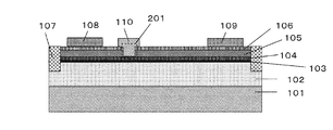
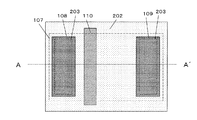
以下、第1の実施の形態に係る電界効果トランジスタを製造方法とともに説明する。図1は第1の実施の形態に係る電界効果トランジスタの上面図、図2は図1のA−A´線に沿って切った断面図である。
(First embodiment)
The field effect transistor according to the first embodiment will be described below together with the manufacturing method. FIG. 1 is a top view of the field effect transistor according to the first embodiment, and FIG. 2 is a cross-sectional view taken along the line AA ′ of FIG.
まず、MOCVD法により、主面の面方位が(111)のSiからなる基板101の主面上に、膜厚が2μmの例えばGaNからなるチャネル層102、膜厚が1nmの例えばAlNからなる第一電子障壁層103、膜厚が10nmの例えばAl0.30Ga0.70Nからなる第二電子障壁層104、膜厚が7.5nmの例えばIn0.18Al0.82Nからなる第三電子障壁層105、Mgをドーピングした膜厚が7.5nmの例えばIn0.18Al0.82Nからなる第四電子障壁層106を順次成長する。第一電子障壁層103、第二電子障壁層104、第三電子障壁層105、第四電子障壁層106にて電子供給層が形成されている。次に、レジストパターニング後にたとえばBイオンを注入することによりイオン注入部107を形成する。次に、たとえばTi/Al(20nm/200nm)からなるソース電極108およびドレイン電極109を前記第四電子障壁層106の上に順次形成する。次に、たとえばNi/Au(膜厚100nm/500nm)からなるゲート電極110を形成する。
First, by MOCVD, a
ここで、第四電子障壁層106のMgの濃度は、5×1018cm-3であり、第四電子障壁層106内のドナーを十分に自己補償する濃度である。なお、Mgの濃度は2次イオン質量分析法(SIMS)にて測定した。
Here, the Mg concentration of the fourth
第四電子障壁層106のMgの濃度が5×1018cm-3であるとき、第四電子障壁層106内のドナーが十分に自己補償されるのは、以下の理由による。
When the Mg concentration of the fourth
すなわち、第四電子障壁層106はInAlGaNからなり、Mgを添加しない場合はn型となり1017cm-3〜1018cm-3程度のキャリア濃度を有する。一方、例えばGaNの場合ではMgの濃度が5×1018cm-3であるとき、p型キャリア濃度は8×1017cm-3である。すなわち、第四電子障壁層106に5×1018cm-3の濃度のMgを添加した場合、8×1017cm-3程度のp型キャリアが生じることになる。このp型キャリアとMgを添加しない場合に生じるn型キャリアが相殺する。このようにして、第四電子障壁層106内のドナーが十分に自己補償されるのである。
That is, the fourth
ソース電極108およびドレイン電極109は、チャネル層102とオーミック的に導通し、ゲート電極110は第四電子障壁層106に対してショットキー接触をする。ソース電極108およびドレイン電極109がチャネル層102とオーミック的に導通するのは、第一電子障壁層103、第二電子障壁層104および第三電子障壁層105がn型であり、第四電子障壁層106の層厚が薄いからである。
The
なお、チャネル層102、第一電子障壁層103、第二電子障壁層104、第三電子障壁層105および第四電子障壁層106の主面の面方位は(0001)面(c面)である。
The plane orientations of the main surfaces of the
上記により製造された本発明に電界効果トランジスタの層構造については、以下の表1のようになる。 The layer structure of the field effect transistor according to the present invention manufactured as described above is as shown in Table 1 below.

また、本発明の電界効果トランジスタについて、ゲート電極110の長手方向は<11−20>方向としている。従って、ソース電極108とゲート電極110とを結ぶ方向は<1−100>方向である。ゲート長(ゲート電極110の<1−100>方向に沿った幅)は2μmであり、ソース電極108とゲート電極110との向かい合う両端の電極間距離は1.5μmであり、ドレイン電極109とゲート電極110との向かい合う両端の電極間距離は10μmである。また、電界効果トランジスタの素子サイズは<11−20>方向に250μmであり、<1−100>方向に250μmである。イオン注入部107は、電界効果トランジスタの端部より20μmの位置まで設けられている。
In the field effect transistor of the present invention, the longitudinal direction of the
なお、GaNと格子整合したInAlGaNの臨界膜厚は、理論上無限大となるはずであるが、実際には膜厚50nm以上堆積させると急激に結晶性が低下する。 Note that the critical film thickness of InAlGaN lattice-matched with GaN should theoretically be infinite, but in reality, when the film thickness is 50 nm or more, the crystallinity is drastically lowered.
ここで、膜厚をd、基板とエピタキシャル膜の格子定数差Δaと基板の格子定数aの比Δa/aを格子不整合度と定義すると、クラックが入らない良好な結晶を得るためには Here, when the film thickness is d and the ratio Δa / a of the lattice constant a between the substrate and the epitaxial film and the lattice constant a of the substrate is defined as the degree of lattice mismatch, in order to obtain a good crystal without cracks,
![]()
![]()
を満たすような格子不整合度が好ましいことを実験的に確認した。さらに、この条件の中でも第三電子障壁層105、第四電子障壁層106の膜厚は、合計して50nm以下であることが特に好ましい。
It was experimentally confirmed that a lattice mismatch degree satisfying the above condition is preferable. Furthermore, among these conditions, the total thickness of the third
この第の実施の形態に係る電界トランジスタの特性について、以下に説明する。 The characteristics of the field transistor according to the first embodiment will be described below.
ここで検討した電界効果トランジスタとしては、第三電子障壁層105および第四電子障壁層106がともにアンドープであるサンプル(サンプルA)、第三電子障壁層105および第四電子障壁層106中に一様にMgをドーピングしたサンプル(サンプルB)、第三電子障壁層105をアンドープとし、第四電子障壁層106にMgをドーピングしたサンプル(サンプルC)の3種類である。なお、サンプルBおよびサンプルCにおいてドープされた層のMg濃度は、ともに5×1018cm-3であり、層内のドナーを十分に自己補償する濃度である。
As the field effect transistor examined here, the third
検討したサンプルについて、第三電子障壁層105および第四電子障壁層106のMgドープの有無とMg濃度との関係は、表2のようになる。
Table 2 shows the relationship between the presence or absence of Mg doping in the third
(1)オフ耐圧特性
まず、上記サンプルA〜Cについて、ゲート電極110とドレイン電極109との間の距離をパラメータとし、ゲート電極110に電圧を印加してオフ耐圧を測定した。ここで、オフ耐圧とは、電界効果トランジスタのゲート電圧をしきい値電圧以下(つまりオフ状態)にした状態でのソースとレインとの間の耐圧のことをいう。その結果、図3に示す結果が得られた。図3より、サンプルAと比べてサンプルBおよびサンプルCのオフ耐圧が向上していることがわかる。ゲート電極110とドレイン電極109との間の距離が10μmのとき、オフ耐圧は表3のようになる。
(1) Off-breakdown voltage characteristics First, with respect to the samples A to C, the distance between the
表3より、第四電子障壁層106にMgをドーピングしていないサンプルAのオフ耐圧は60Vであり、第四電子障壁層106にMgをドーピングしたサンプルBおよびサンプルCのオフ耐圧は、ともに400Vであることがわかった。このことから、第四電子障壁層106にMgをドーピングすることで、オフ耐圧が60V程度から400V超まで飛躍的に向上したことがわかった。
From Table 3, the off breakdown voltage of sample A in which Mg is not doped in the fourth
このオフ耐圧の向上について以下に説明する。 The improvement of the off breakdown voltage will be described below.
第三電子障壁層105と第四電子障壁層106の結晶成長時、蒸気圧の高いInを取り込みやすくするため、第三電子障壁層105および第四電子障壁層106がAlGaNの場合よりも100℃程度結晶成長温度を低くする必要がある。しかしながら、結晶成長温度が低いとIII族窒化物半導体を構成する原子が結晶表面を十分にマイグレーションしなくなるため、結晶欠陥が生成されやすくなる。この場合、結晶欠陥の中でも特に窒素空孔が形成されているものと考えられる。窒素空孔はIII族窒化物半導体においてドナーとして働くため、ドーピングを行わなくても結晶がn型化する。
During the crystal growth of the third
従って、第三電子障壁層105と第四電子障壁層106にInAlGaNを用いた場合、リーク電流が多くなり、アバランシェ破壊も生じやすくなることでオフ耐圧が低下するものと考えられる。
Therefore, when InAlGaN is used for the third
そこで、本願発明者らは、InAlGaNの第三電子障壁層105と第四電子障壁層106とにMgをドーピングすることにより正孔を生じさせ、窒素空孔によって生じた電子を正孔によって自己補償させることを試みた。その結果、リーク電流が低減し、オフ耐圧が向上することがわかった。
Therefore, the inventors of the present application generated holes by doping Mg into the third
結果として、ゲート電極110とドレイン電極109との間距離が10μmでオフ耐圧は60Vしかなかったものが400Vまで改善したのである。
As a result, the distance between the
なお、オフ耐圧の向上から、第四電子障壁層106は高抵抗または半絶縁性となっていることがわかった。
(2)Id−Vd特性
次に、サンプルA、サンプルBおよびサンプルCに関するドレイン電流・ドレイン電圧特性(以下、Id−Vd特性という)について説明する。
In addition, it turned out that the 4th
(2) Id-Vd Characteristics Next, drain current / drain voltage characteristics (hereinafter referred to as Id-Vd characteristics) regarding Sample A, Sample B, and Sample C will be described.
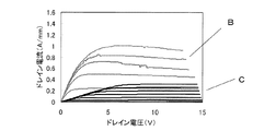
まず、サンプルAとサンプルBとについて、Id−Vd特性を図4に示す。図4において、横軸がドレイン電圧(単位はV)、縦軸がドレイン電流(単位はA/mm)であり、グラフAはサンプルAに関するグラフであり、グラフBはサンプルBに関するグラフである。なお、ゲート電圧は、それぞれのグラフについて−2V〜6Vの間で1Vステップにて変化させている。 First, the Id-Vd characteristics of Sample A and Sample B are shown in FIG. In FIG. 4, the horizontal axis represents the drain voltage (unit: V), the vertical axis represents the drain current (unit: A / mm), graph A is a graph related to sample A, and graph B is a graph related to sample B. The gate voltage is changed in a 1V step between -2V to 6V for each graph.
サンプルBのように電子を十分に自己補償させるほどのMgを第三電子障壁層105および第四電子障壁層106にドーピングすると、Mgをドーピングしていない場合(サンプルA)と比較して著しく最大ドレイン電流が減少した。これは、Mgドーピングに伴う不純物散乱の増大により電子移動度が著しく低下してシート抵抗が増大したことによるものと推定される。
When Mg which sufficiently self-compensates electrons as in Sample B is doped into the third
次に、上記サンプルBおよびサンプルCについて、ドレイン電流ドレイン電圧特性を調べた、その結果を図5に示す。図5において、横軸がドレイン電圧(単位はV)、縦軸がドレイン電流(単位はA/mm)であり、グラフBはサンプルBに関するグラフであり、グラフCはサンプルCに関するグラフである。なお、ゲート電圧は、それぞれのグラフについて−2V〜6Vの間で1Vステップにて変化させている。図4より、ドレイン電流ドレイン電圧特性サンプルBについては大幅に電流が低減したのに対し、サンプルCについてはサンプルAと同等のドレイン電流が得られた。 Next, the drain current drain voltage characteristics of the sample B and the sample C were examined, and the results are shown in FIG. In FIG. 5, the horizontal axis is the drain voltage (unit is V), the vertical axis is the drain current (unit is A / mm), the graph B is a graph regarding the sample B, and the graph C is a graph regarding the sample C. The gate voltage is changed in a 1V step between -2V to 6V for each graph. From FIG. 4, the drain current drain voltage characteristic sample B was significantly reduced in current, while sample C had a drain current equivalent to that of sample A.
以上のように、本実施の形態によれば、オフ耐圧が飛躍的に向上するとともに大電流の電界効果トランジスタを実現できることがわかった。 As described above, according to the present embodiment, it has been found that the off-breakdown voltage is dramatically improved and a large-current field effect transistor can be realized.
なお、Mg濃度が5×1017cm-3以上5×1020cm-3以下、特にMg濃度が5×1018cm-3以上5×1019cm-3であれば、第四電子障壁層106において層内のドナーを十分に自己補償できて好適な第四電子障壁層106が得られる。
If the Mg concentration is 5 × 10 17 cm −3 or more and 5 × 10 20 cm −3 or less, particularly if the Mg concentration is 5 × 10 18 cm −3 or more and 5 × 10 19 cm −3 , the fourth electron barrier layer. In 106, the donor in the layer can be sufficiently self-compensated to obtain a suitable fourth
また、上記実施の形態においては、第三電子障壁層の組成と第四電子障壁層の組成とを等しくしているが、第三電子障壁層の組成と第四電子障壁層の組成は必ずしも等しくなくてもよい。 In the above embodiment, the composition of the third electron barrier layer and the composition of the fourth electron barrier layer are equal, but the composition of the third electron barrier layer and the composition of the fourth electron barrier layer are not necessarily equal. It does not have to be.
第四電子障壁層106の上にゲート電極110が形成されている場合、ゲート電極110の端部に電界集中がしやすくなるので、第四電子障壁層106のオフ耐圧を特に高くするのが好ましい。
In the case where the
一般的に、InAlGaNのIn組成を高くしてMgのドーピングを過剰に行うと、Mgがアクセプタとして働く格子位置に納まらず、ドナーとしても働くようになるため、第四電子障壁層106のIn組成は、オフ耐圧向上を目的とする場合は低い方が好ましい。
In general, when Mg is excessively doped by increasing the In composition of InAlGaN, Mg does not fit in the lattice position where it acts as an acceptor, and it also acts as a donor. Therefore, the In composition of the fourth
しかしながら、第四電子障壁層106のIn組成を下げた場合、電流が減少してしまうというトレードオフが起きるので、オフ耐圧と大電流化を両立したい場合は第四電子障壁層106の組成は、第三電子障壁層105と同一組成であることが好ましい。
However, when the In composition of the fourth
また、InAlGaNはIn、Al、Ga、そしてNから成る四元混晶であるため、In組成が高くなるほど合金散乱による移動度低下が著しい。そこで、第二電子障壁層104と第三電子障壁層105との間には、第二電子障壁層104および第三電子障壁層105よりもバンドギャップが小さく、第三電子障壁層105よりもIn組成の小さい窒化物半導体層が挿入されていてもよい。これにより、InAlGaNの合金散乱の抑制がなされ移動度の向上によりシート抵抗を低減することができる。
Further, since InAlGaN is a quaternary mixed crystal composed of In, Al, Ga, and N, the lower the mobility due to alloy scattering, the higher the In composition. Therefore, the band gap between the second
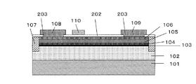
(第2の実施の形態)
以下、第2の実施の形態に係る電界効果トランジスタを製造方法とともに説明する。図6は第2の実施の形態に係る電界効果トランジスタの上面図、図7は図6のA−A´線に沿って切った断面図である。図6、図7において、図2、図3と同一の要素は同一の符号を付与し説明を省略する。第1の実施例と同様にして、MOCVD法により基板101上にチャネル層102、第一電子障壁層103、第二電子障壁層104、第三電子障壁層105、第四電子障壁層106を順次堆積させる。次に、レジストパターニング後にたとえばBイオンを注入することによりイオン注入部107を形成する。次に、レジストパターニングの後にドライエッチングをすることにより、リセス部201を形成する。しきい値電圧が過度にマイナス側に大きくならないよう、リセス部201の底面は第一電子障壁層103、もしくは第二電子障壁層104に達するようにする。本実施の形態においては、第一電子障壁層103の上面に達するようにリセス部201を形成している。
(Second Embodiment)
The field effect transistor according to the second embodiment will be described below together with the manufacturing method. FIG. 6 is a top view of the field effect transistor according to the second embodiment, and FIG. 7 is a cross-sectional view taken along the line AA ′ of FIG. 6 and FIG. 7, the same elements as those in FIG. 2 and FIG. Similarly to the first embodiment, the
なお、リセス部201については、リセス幅(<1−100>方向に沿った幅)は1μmである。その他電界効果トランジスタに関するパラメータは、第1の実施の形態と同様である。
For the
次に、ソース電極108およびドレイン電極109を第四電子障壁層106の上に順次形成する。次に、ゲート電極110をリセス部201の上に形成する。
Next, the
ここで検討した電界効果トランジスタとして、リセス部201があるサンプルをサンプルD、リセス部201がないサンプルをサンプルEとする。サンプルDおよびサンプルEに対し、しきい値電圧を調べたところ、表4のようになった。
As the field effect transistor examined here, a sample with the
![]()
![]()
リセス部201がないサンプルEの場合はゲート電極110の下部のキャリア密度が非常に高く、しきい値電圧が−15V以下となっていたが、前記リセス部201を有するサンプルDの場合はしきい値電圧を−3V程度とすることができる。
In the case of sample E without the
以上のように、本実施の形態によれば、オフ耐圧が飛躍的に向上するとともにしきい値電圧を−3V程度に制御した大電流の電界効果トランジスタを実現できる。 As described above, according to the present embodiment, it is possible to realize a large-current field effect transistor in which the off breakdown voltage is dramatically improved and the threshold voltage is controlled to about −3V.
なお、リセス部201の底面は、第一電子障壁層103の層厚が薄いほどしきい値電圧が正にシフトする。しかしながら第一電子障壁層103の層厚が薄くなるようにリセス部201を形成した場合、第三電子障壁層105が窒素空孔形成によりn型化しているため、ゲート電極110が第三電子障壁層105に接しているとリーク電流増大の原因となるため、例えば第三電子障壁層105のゲート電極110が接する部分にはイオン注入等により高抵抗化したり、または絶縁層を形成することにより、ゲートリーク電流を低減させることが好ましい。
Note that the threshold voltage of the bottom surface of the
(第3の実施の形態)
以下、第3の実施の形態に係る窒化物半導体素子を製造方法とともに説明する。図8は第3の実施の形態に係る電界効果トランジスタの上面図、図9は図8のA−A´線に沿って切った断面図である。図8、図9において、図2、図3と同一の要素は同一の符号を付与し説明を省略する。第1の実施例と同様にして、MOCVD法により基板101上にチャネル層102、第一電子障壁層103、第二電子障壁層104、第三電子障壁層105、第四電子障壁層106を順次堆積させる。次に、レジストパターニング後にたとえばBイオンを注入することによりイオン注入部107を形成する。次に、レジストパターニング後にドライエッチすることによりリセス部201を形成し、第四電子障壁層106の上にソース電極108、ドレイン電極109、前記リセス部201の上にゲート電極110を形成する。実施例2においてはゲート電極と第三電子障壁層105、第四電子障壁層106が接していたが、本実施の形態においては、図9に示すように、リセス部201の幅がゲート電極110の幅よりも広く、ゲート電極110と第三電子障壁層105、第四電子障壁層106と接しない構成となっている。なお、本実施の形態においては、第一電子障壁層103の上面に達するようにリセス部201が形成されている。
(Third embodiment)
The nitride semiconductor device according to the third embodiment will be described below together with the manufacturing method. FIG. 8 is a top view of a field effect transistor according to the third embodiment, and FIG. 9 is a cross-sectional view taken along the line AA ′ of FIG. 8 and 9, the same elements as those in FIGS. 2 and 3 are denoted by the same reference numerals, and the description thereof is omitted. Similarly to the first embodiment, the
なお、リセス部201については、リセス幅(<1−100>方向に沿った幅)は1μmである。その他電界効果トランジスタに関するパラメータは、第1の実施の形態と同様である。
For the
第三電子障壁層105はInを含んでおり、窒素空孔が多い。そのため、第三電子障壁層105とゲート電極110とを離間させることによってゲートリーク電流を抑制できる。この第3の実施の形態に係る電界効果トランジスタについては、第2の実施の形態の場合と同様に、リセス部201を有することによりしきい値電圧を−3V程度とすることができた。
The third
以上のように、本実施の形態によれば、オフ耐圧が飛躍的に向上するとともにしきい値電圧を−3V程度に制御した大電流の電界効果トランジスタを実現できる。 As described above, according to the present embodiment, it is possible to realize a large-current field effect transistor in which the off breakdown voltage is dramatically improved and the threshold voltage is controlled to about −3V.
(第4の実施の形態)
以下、第4の実施の形態に係る窒化物半導体素子を製造方法とともに説明する。図10は第4の実施の形態に係る電界効果トランジスタの上面図、図11は図10のA−A´線に沿って切った断面図である。図10、図11において、図2、図3と同一の要素は同一の符号を付与し説明を省略する。
(Fourth embodiment)
The nitride semiconductor device according to the fourth embodiment will be described below together with the manufacturing method. FIG. 10 is a top view of a field effect transistor according to the fourth embodiment, and FIG. 11 is a cross-sectional view taken along the line AA ′ of FIG. 10 and FIG. 11, the same elements as those in FIG. 2 and FIG.
第1の実施の形態と同様にして、MOCVD法により基板101上にチャネル層102、第一電子障壁層103、第二電子障壁層104、第三電子障壁層105、第四電子障壁層106を順次堆積させる。次に、レジストパターニング後にたとえばBイオンを注入することによりイオン注入部107を形成する。次に第四電子障壁層106を覆うように、例えば層厚が100nmのSiNからなる絶縁膜202を形成する。次に、レジストパターングにより第四電子障壁層106の上にオーミック窓部203を形成する。次に、オーミック窓部203の上にソース電極108、ドレイン電極109を形成する。次に、リセス部201および絶縁膜202の上にゲート電極110を形成する。
Similarly to the first embodiment, the
なお、本実施の形態においては、第一電子障壁層103の上面に達するようにリセス部201が形成されている。
In the present embodiment, the
なお、リセス部201については、リセス幅(<1−100>方向に沿った幅)は1μmである。その他電界効果トランジスタに関するパラメータは、第1の実施の形態と同様である。
For the
このようにして製造された第3の実施の形態に係る電界効果トランジスタについては、絶縁膜202によりゲートリーク電流が抑制される。
In the field effect transistor according to the third embodiment manufactured as described above, the gate leakage current is suppressed by the insulating
以上のように、本実施の形態によれば、オフ耐圧が飛躍的に向上するとともに大電流・低ゲートリーク電流の電界効果トランジスタを実現できる。 As described above, according to the present embodiment, it is possible to realize a field effect transistor having a large off-breakdown voltage and a large current / low gate leakage current.
(第5の実施の形態)
以下、第5の実施の形態に係る窒化物半導体素子を製造方法とともに説明する。図12は第5の実施の形態に係る電界効果トランジスタの上面図、図13は図12のA−A´線に沿って切った断面図である。図12、図13において、図2、図3と同一の要素は同一の符号を付与し説明を省略する。
(Fifth embodiment)
A nitride semiconductor device according to the fifth embodiment will be described below together with a manufacturing method. FIG. 12 is a top view of a field effect transistor according to the fifth embodiment, and FIG. 13 is a cross-sectional view taken along the line AA ′ of FIG. 12 and 13, the same elements as those in FIGS. 2 and 3 are given the same reference numerals and description thereof is omitted.
第1の実施の形態と同様にして、MOCVD法により基板101上にチャネル層102、第一電子障壁層103、第二電子障壁層104、第三電子障壁層105、第四電子障壁層106を順次堆積させる。次に、レジストパターニング後にたとえばBイオンを注入することによりイオン注入部107を形成する。次に、レジストパターニング後にドライエッチすることによりリセス部201を形成する。次に、リセス部201上と第四電子障壁層106を覆うように、例えばSiNからなる絶縁膜202を形成する。次に、レジストパターニングにより第四電子障壁層106の上にオーミック窓部203を形成する。次に、オーミック窓部203の上にソース電極108、ドレイン電極109を形成する。次に、リセス部201および絶縁膜202上にゲート電極110を形成する。
Similarly to the first embodiment, the
なお、本実施の形態においては、第一電子障壁層103の上面に達するようにリセス部201が形成されている。
In the present embodiment, the
なお、リセス部201については、リセス幅(<1−100>方向に沿った幅)は1μmである。その他電界効果トランジスタに関するパラメータは、第1の実施の形態と同様である。
For the
絶縁膜202によりゲートリーク電流が抑制され、リセス部201を有することにより、第4の実施の形態の電界効果トランジスタよりもしきい値電圧を正にシフトすることができる。
Since the gate leakage current is suppressed by the insulating
以上のように、本実施の形態によれば、しきい値電圧を制御するとともにオフ耐圧が飛躍的に向上するとともに大電流・低ゲートリーク電流の電界効果トランジスタを実現できる。 As described above, according to the present embodiment, it is possible to realize a field effect transistor having a large current and a low gate leakage current while controlling the threshold voltage and dramatically improving the off breakdown voltage.
(第6の実施の形態)
以下、第6の実施の形態に係る窒化物半導体素子を製造方法とともに説明する。図14は第6の実施の形態に係る電界効果トランジスタの上面図、図15は図14のA−A´線に沿って切った断面図である。図14、図15において、図2、図3と同一の要素は同一の符号を付与し説明を省略する。
(Sixth embodiment)
The nitride semiconductor device according to the sixth embodiment will be described below together with the manufacturing method. FIG. 14 is a top view of a field effect transistor according to the sixth embodiment, and FIG. 15 is a cross-sectional view taken along the line AA ′ of FIG. 14 and FIG. 15, the same elements as those in FIG. 2 and FIG.
第1の実施の形態と同様にして、MOCVD法により基板101上にチャネル層102、第一電子障壁層103、第二電子障壁層104、第三電子障壁層105、第四電子障壁層106を順次堆積させる。次に、レジストパターニング後にたとえばBイオンを注入することによりイオン注入部107を形成する。次に、レジストパターニング後にドライエッチすることによりリセス部201を形成する。次に、リセス部201上と第四電子障壁層106を覆うように、例えばSiNからなる絶縁膜202を形成する。次に、レジストパターングにより第四電子障壁層106上にオーミック窓部203を形成する。次に、オーミック窓部203上にソース電極108、ドレイン電極109を形成する。次に、リセス部201および絶縁膜202上にゲート電極110を形成する。第5の実施の形態においてはゲート電極110の側面と絶縁膜202が接していたが、本実施の形態においては、図15に示すように、リセス部201の幅がゲート電極110の幅よりも広く、ゲート電極110の側面と絶縁膜202とが接しない構成となっている。
Similarly to the first embodiment, the
なお、本実施の形態においては、第一電子障壁層103の上面に達するようにリセス部201が形成されている。
In the present embodiment, the
なお、リセス部201については、リセス幅(<1−100>方向に沿った幅)は1μmである。その他電界効果トランジスタに関するパラメータは、第1の実施の形態と同様である。
For the
本実施の形態にかかる電界効果トランジスタについては、第三電子障壁層105において生じた電子が絶縁膜202をトンネルしてゲート電極110に到達することがなく、第5の実施の形態にかかる電界効果トランジスタよりもさらにゲートリーク電流を抑制できる構成となっている。また、第5の実施の形態と同様にリセス部201を有することにより、第4の実施の形態にかかる電界効果トランジスタよりもしきい値電圧を正にシフトすることができる。
In the field effect transistor according to the present embodiment, the electrons generated in the third
以上のように、本実施の形態によれば、しきい値電圧を制御するとともにオフ耐圧が飛躍的に向上するとともに大電流・低ゲートリーク電流の電界効果トランジスタを実現できる。 As described above, according to the present embodiment, it is possible to realize a field effect transistor having a large current and a low gate leakage current while controlling the threshold voltage and dramatically improving the off breakdown voltage.
なお、上記第1ないし第6の実施の形態において、電界効果トランジスタを構成する各半導体層の組成や層厚、リセス部201の幅は上記に限定されない。また、ソース電極108、ドレイン電極109およびゲート電極110を構成する電極金属やその膜厚は上記に限定されない。また、イオン注入部107の領域は、上記に限定されない。
In the first to sixth embodiments, the composition and thickness of each semiconductor layer constituting the field effect transistor and the width of the
また、上記第4の実施の形態において、絶縁膜202はSiNに限らず、SiO2やSiON(シリコン酸窒化膜)、その他酸化アルミニウム、窒化アルミニウム等を用いてもよい。
In the fourth embodiment, the insulating
また、上記第1ないし第6の実施の形態において、基板101としては、主面を(111)とするSi以外にサファイア、炭化珪素、窒化ガリウム、窒化アルミニウム、酸化ガリウム等を用いることができる。
In the first to sixth embodiments, sapphire, silicon carbide, gallium nitride, aluminum nitride, gallium oxide, or the like can be used as the
また、上記第1ないし第6の実施の形態において、アクセプタ性の不純物としてMgを用いたが、Mg以外にBe、C、Znを用いてもよい。 In the first to sixth embodiments, Mg is used as the acceptor impurity, but Be, C, and Zn may be used in addition to Mg.
また、上記第1ないし第6の実施の形態において、アクセプタ性の不純物としてMgを用いたが、Mg以外にBe、C、Znを用いてもよい。 In the first to sixth embodiments, Mg is used as the acceptor impurity, but Be, C, and Zn may be used in addition to Mg.
本発明にかかる電界効果トランジスタは、Inを含む窒化物半導体よりなる電子障壁層にMgをドープすることによりゲートリーク電流を抑制でき、かつオフ耐圧を向上させることができるものである、この電界効果トランジスタは、空調や自動車の制御といった、高耐圧が求められるパワーデバイスの分野に大いに利用できるものである。 The field effect transistor according to the present invention is capable of suppressing a gate leakage current and improving an off breakdown voltage by doping Mg into an electron barrier layer made of a nitride semiconductor containing In. Transistors can be used greatly in the field of power devices that require high breakdown voltage, such as air conditioning and automobile control.
101 基板
102 チャネル層
103 第一電子障壁層
104 第二電子障壁層
105 第三電子障壁層
106 第四電子障壁層
107 イオン注入部
108 ソース電極
109 ドレイン電極
110 ゲート電極
201 リセス部
202 絶縁膜
203 オーミック窓部
DESCRIPTION OF
Claims (13)
前記基板の上に配置された、第1の窒化物半導体よりなるチャネル層と、
前記チャネル層の上に形成された電子供給層と、
前記電子供給層の上に形成されたソース電極、ゲート電極およびドレイン電極と、を有し、
前記電子供給層は、前記第1の窒化物半導体よりもバンドギャップが大きい第2の窒化物半導体よりなる層と、前記第2の窒化物半導体よりなる層の上に形成された、Inを含有し、かつ前記第1の窒化物半導体よりもバンドギャップが大きい第3の窒化物半導体よりなる層と、を有し、
前記第3の窒化物半導体よりなる層は、アクセプタ性不純物が添加されてドナーが補償されており、
前記電子供給層には、前記第3の窒化物半導体よりなる層に達するリセス部が設けられ、前記リセス部の底部に前記ゲート電極が形成され、
前記リセス部の幅は、前記ゲート電極の幅よりも広く、前記ゲート電極と前記第3の窒化物半導体よりなる層とは離間していることを特徴とする電界効果トランジスタ。 A substrate,
A channel layer made of a first nitride semiconductor and disposed on the substrate;
An electron supply layer formed on the channel layer;
A source electrode, a gate electrode and a drain electrode formed on the electron supply layer,
The electron supply layer contains In, formed on a layer made of a second nitride semiconductor having a band gap larger than that of the first nitride semiconductor and a layer made of the second nitride semiconductor. And a layer made of a third nitride semiconductor having a band gap larger than that of the first nitride semiconductor,
In the third nitride semiconductor layer, acceptor impurities are added to compensate the donor ,
The electron supply layer is provided with a recess that reaches the layer made of the third nitride semiconductor, and the gate electrode is formed at the bottom of the recess,
The width of the recess is wider than the width of the gate electrode, and the gate electrode and the third nitride semiconductor layer are separated from each other .
前記第2の窒化物半導体よりなる層と前記第4の窒化物半導体よりなる層との間に配置された第5の窒化物半導体よりなる層を備え、
前記第5の窒化物半導体のバンドギャップは、前記第4の窒化物半導体のバンドギャップよりも小さいことを特徴とする、請求項5または6に記載の電界効果トランジスタ。 The electron supply layer is
A fifth nitride semiconductor layer disposed between the second nitride semiconductor layer and the fourth nitride semiconductor layer;
The field effect transistor according to claim 5 or 6, wherein a band gap of the fifth nitride semiconductor is smaller than a band gap of the fourth nitride semiconductor.
Priority Applications (1)
| Application Number | Priority Date | Filing Date | Title |
|---|---|---|---|
| JP2014031344A JP6233088B2 (en) | 2014-02-21 | 2014-02-21 | Field effect transistor |
Applications Claiming Priority (1)
| Application Number | Priority Date | Filing Date | Title |
|---|---|---|---|
| JP2014031344A JP6233088B2 (en) | 2014-02-21 | 2014-02-21 | Field effect transistor |
Publications (2)
| Publication Number | Publication Date |
|---|---|
| JP2015156454A JP2015156454A (en) | 2015-08-27 |
| JP6233088B2 true JP6233088B2 (en) | 2017-11-22 |
Family
ID=54775598
Family Applications (1)
| Application Number | Title | Priority Date | Filing Date |
|---|---|---|---|
| JP2014031344A Active JP6233088B2 (en) | 2014-02-21 | 2014-02-21 | Field effect transistor |
Country Status (1)
| Country | Link |
|---|---|
| JP (1) | JP6233088B2 (en) |
Families Citing this family (4)
| Publication number | Priority date | Publication date | Assignee | Title |
|---|---|---|---|---|
| CN107924845A (en) * | 2015-08-28 | 2018-04-17 | 夏普株式会社 | Nitride compound semiconductor device |
| JP6792135B2 (en) * | 2015-10-30 | 2020-11-25 | 富士通株式会社 | Compound semiconductor device and its manufacturing method |
| JP6575304B2 (en) * | 2015-10-30 | 2019-09-18 | 富士通株式会社 | Semiconductor device, power supply device, amplifier, and semiconductor device manufacturing method |
| US11240455B2 (en) | 2016-07-28 | 2022-02-01 | Sony Semiconductor Solutions Corporation | Ad conversion device, ad conversion method, image sensor, and electronic apparatus |
Family Cites Families (9)
| Publication number | Priority date | Publication date | Assignee | Title |
|---|---|---|---|---|
| JP2001185717A (en) * | 1999-12-22 | 2001-07-06 | Toshiba Corp | Semiconductor device and method of manufacturing it |
| JP2002319702A (en) * | 2001-04-19 | 2002-10-31 | Sony Corp | Method of manufacturing nitride semiconductor element and nitride semiconductor element |
| JP2005243719A (en) * | 2004-02-24 | 2005-09-08 | Yasuo Ono | Field effect transistor and its manufacturing method |
| JP2005268493A (en) * | 2004-03-18 | 2005-09-29 | National Institute Of Information & Communication Technology | Hetero junction field effect transistor |
| JP2010040828A (en) * | 2008-08-06 | 2010-02-18 | Nippon Telegr & Teleph Corp <Ntt> | Nitride semiconductor device |
| WO2011039800A1 (en) * | 2009-09-29 | 2011-04-07 | 株式会社 東芝 | Semiconductor device |
| JP5724347B2 (en) * | 2010-12-10 | 2015-05-27 | 富士通株式会社 | Compound semiconductor device and manufacturing method thereof |
| JP2013168433A (en) * | 2012-02-14 | 2013-08-29 | Toshiba Corp | Nitride semiconductor device and method of manufacturing nitride semiconductor device |
| JP5656930B2 (en) * | 2012-07-05 | 2015-01-21 | 古河電気工業株式会社 | Nitride compound semiconductor device |
-
2014
- 2014-02-21 JP JP2014031344A patent/JP6233088B2/en active Active
Also Published As
| Publication number | Publication date |
|---|---|
| JP2015156454A (en) | 2015-08-27 |
Similar Documents
| Publication | Publication Date | Title |
|---|---|---|
| JP6439789B2 (en) | Field effect transistor | |
| US10756207B2 (en) | Lateral III-nitride devices including a vertical gate module | |
| US11322599B2 (en) | Enhancement mode III-nitride devices having an Al1-xSixO gate insulator | |
| US9490324B2 (en) | N-polar III-nitride transistors | |
| US10043896B2 (en) | III-Nitride transistor including a III-N depleting layer | |
| US10229992B2 (en) | Semiconductor device and manufacturing method of semiconductor device | |
| US7612390B2 (en) | Heterojunction transistors including energy barriers | |
| US7170111B2 (en) | Nitride heterojunction transistors having charge-transfer induced energy barriers and methods of fabricating the same | |
| WO2010109566A1 (en) | Semiconductor device and method for manufacturing same | |
| US7985984B2 (en) | III-nitride semiconductor field effect transistor | |
| US9219136B2 (en) | Switching element | |
| US20150263155A1 (en) | Semiconductor device | |
| WO2015008430A1 (en) | Semiconductor device | |
| JP2012227456A (en) | Semiconductor device | |
| US20160211357A1 (en) | Semiconductor device | |
| JP6233088B2 (en) | Field effect transistor | |
| US9343544B2 (en) | Multi-finger large periphery AlInN/AlN/GaN metal-oxide-semiconductor heterostructure field effect transistors on sapphire substrate | |
| CN103003930B (en) | Field-effect transistor | |
| KR101200274B1 (en) | Enhancement normally off nitride vertical semiconductor device and manufacturing method thereof | |
| WO2020217735A1 (en) | Nitride semiconductor device | |
| US10158012B1 (en) | Semiconductor device | |
| US20200091330A1 (en) | Semiconductor device |
Legal Events
| Date | Code | Title | Description |
|---|---|---|---|
| A621 | Written request for application examination |
Free format text: JAPANESE INTERMEDIATE CODE: A621 Effective date: 20160823 |
|
| RD01 | Notification of change of attorney |
Free format text: JAPANESE INTERMEDIATE CODE: A7421 Effective date: 20170417 |
|
| A977 | Report on retrieval |
Free format text: JAPANESE INTERMEDIATE CODE: A971007 Effective date: 20170519 |
|
| A131 | Notification of reasons for refusal |
Free format text: JAPANESE INTERMEDIATE CODE: A131 Effective date: 20170530 |
|
| A521 | Request for written amendment filed |
Free format text: JAPANESE INTERMEDIATE CODE: A523 Effective date: 20170721 |
|
| TRDD | Decision of grant or rejection written | ||
| A01 | Written decision to grant a patent or to grant a registration (utility model) |
Free format text: JAPANESE INTERMEDIATE CODE: A01 Effective date: 20170926 |
|
| A61 | First payment of annual fees (during grant procedure) |
Free format text: JAPANESE INTERMEDIATE CODE: A61 Effective date: 20171009 |
|
| R150 | Certificate of patent or registration of utility model |
Ref document number: 6233088 Country of ref document: JP Free format text: JAPANESE INTERMEDIATE CODE: R150 |