JP6232052B2 - Organic light emitting device and method - Google Patents
Organic light emitting device and method Download PDFInfo
- Publication number
- JP6232052B2 JP6232052B2 JP2015509505A JP2015509505A JP6232052B2 JP 6232052 B2 JP6232052 B2 JP 6232052B2 JP 2015509505 A JP2015509505 A JP 2015509505A JP 2015509505 A JP2015509505 A JP 2015509505A JP 6232052 B2 JP6232052 B2 JP 6232052B2
- Authority
- JP
- Japan
- Prior art keywords
- light emitting
- layer
- light
- emitting layer
- substituted
- Prior art date
- Legal status (The legal status is an assumption and is not a legal conclusion. Google has not performed a legal analysis and makes no representation as to the accuracy of the status listed.)
- Expired - Fee Related
Links
Images

Classifications
-
- H—ELECTRICITY
- H10—SEMICONDUCTOR DEVICES; ELECTRIC SOLID-STATE DEVICES NOT OTHERWISE PROVIDED FOR
- H10K—ORGANIC ELECTRIC SOLID-STATE DEVICES
- H10K50/00—Organic light-emitting devices
- H10K50/10—OLEDs or polymer light-emitting diodes [PLED]
- H10K50/11—OLEDs or polymer light-emitting diodes [PLED] characterised by the electroluminescent [EL] layers
- H10K50/12—OLEDs or polymer light-emitting diodes [PLED] characterised by the electroluminescent [EL] layers comprising dopants
- H10K50/121—OLEDs or polymer light-emitting diodes [PLED] characterised by the electroluminescent [EL] layers comprising dopants for assisting energy transfer, e.g. sensitization
-
- C—CHEMISTRY; METALLURGY
- C09—DYES; PAINTS; POLISHES; NATURAL RESINS; ADHESIVES; COMPOSITIONS NOT OTHERWISE PROVIDED FOR; APPLICATIONS OF MATERIALS NOT OTHERWISE PROVIDED FOR
- C09K—MATERIALS FOR MISCELLANEOUS APPLICATIONS, NOT PROVIDED FOR ELSEWHERE
- C09K11/00—Luminescent materials, e.g. electroluminescent or chemiluminescent
- C09K11/06—Luminescent materials, e.g. electroluminescent or chemiluminescent containing organic luminescent materials
-
- H—ELECTRICITY
- H10—SEMICONDUCTOR DEVICES; ELECTRIC SOLID-STATE DEVICES NOT OTHERWISE PROVIDED FOR
- H10K—ORGANIC ELECTRIC SOLID-STATE DEVICES
- H10K50/00—Organic light-emitting devices
- H10K50/10—OLEDs or polymer light-emitting diodes [PLED]
- H10K50/11—OLEDs or polymer light-emitting diodes [PLED] characterised by the electroluminescent [EL] layers
- H10K50/125—OLEDs or polymer light-emitting diodes [PLED] characterised by the electroluminescent [EL] layers specially adapted for multicolour light emission, e.g. for emitting white light
- H10K50/13—OLEDs or polymer light-emitting diodes [PLED] characterised by the electroluminescent [EL] layers specially adapted for multicolour light emission, e.g. for emitting white light comprising stacked EL layers within one EL unit
-
- H—ELECTRICITY
- H10—SEMICONDUCTOR DEVICES; ELECTRIC SOLID-STATE DEVICES NOT OTHERWISE PROVIDED FOR
- H10K—ORGANIC ELECTRIC SOLID-STATE DEVICES
- H10K85/00—Organic materials used in the body or electrodes of devices covered by this subclass
- H10K85/10—Organic polymers or oligomers
- H10K85/111—Organic polymers or oligomers comprising aromatic, heteroaromatic, or aryl chains, e.g. polyaniline, polyphenylene or polyphenylene vinylene
-
- H—ELECTRICITY
- H10—SEMICONDUCTOR DEVICES; ELECTRIC SOLID-STATE DEVICES NOT OTHERWISE PROVIDED FOR
- H10K—ORGANIC ELECTRIC SOLID-STATE DEVICES
- H10K2101/00—Properties of the organic materials covered by group H10K85/00
- H10K2101/10—Triplet emission
-
- H—ELECTRICITY
- H10—SEMICONDUCTOR DEVICES; ELECTRIC SOLID-STATE DEVICES NOT OTHERWISE PROVIDED FOR
- H10K—ORGANIC ELECTRIC SOLID-STATE DEVICES
- H10K2101/00—Properties of the organic materials covered by group H10K85/00
- H10K2101/27—Combination of fluorescent and phosphorescent emission
-
- H—ELECTRICITY
- H10—SEMICONDUCTOR DEVICES; ELECTRIC SOLID-STATE DEVICES NOT OTHERWISE PROVIDED FOR
- H10K—ORGANIC ELECTRIC SOLID-STATE DEVICES
- H10K71/00—Manufacture or treatment specially adapted for the organic devices covered by this subclass
-
- H—ELECTRICITY
- H10—SEMICONDUCTOR DEVICES; ELECTRIC SOLID-STATE DEVICES NOT OTHERWISE PROVIDED FOR
- H10K—ORGANIC ELECTRIC SOLID-STATE DEVICES
- H10K71/00—Manufacture or treatment specially adapted for the organic devices covered by this subclass
- H10K71/10—Deposition of organic active material
- H10K71/12—Deposition of organic active material using liquid deposition, e.g. spin coating
-
- H—ELECTRICITY
- H10—SEMICONDUCTOR DEVICES; ELECTRIC SOLID-STATE DEVICES NOT OTHERWISE PROVIDED FOR
- H10K—ORGANIC ELECTRIC SOLID-STATE DEVICES
- H10K85/00—Organic materials used in the body or electrodes of devices covered by this subclass
- H10K85/10—Organic polymers or oligomers
- H10K85/111—Organic polymers or oligomers comprising aromatic, heteroaromatic, or aryl chains, e.g. polyaniline, polyphenylene or polyphenylene vinylene
- H10K85/115—Polyfluorene; Derivatives thereof
-
- H—ELECTRICITY
- H10—SEMICONDUCTOR DEVICES; ELECTRIC SOLID-STATE DEVICES NOT OTHERWISE PROVIDED FOR
- H10K—ORGANIC ELECTRIC SOLID-STATE DEVICES
- H10K85/00—Organic materials used in the body or electrodes of devices covered by this subclass
- H10K85/10—Organic polymers or oligomers
- H10K85/151—Copolymers
-
- H—ELECTRICITY
- H10—SEMICONDUCTOR DEVICES; ELECTRIC SOLID-STATE DEVICES NOT OTHERWISE PROVIDED FOR
- H10K—ORGANIC ELECTRIC SOLID-STATE DEVICES
- H10K85/00—Organic materials used in the body or electrodes of devices covered by this subclass
- H10K85/30—Coordination compounds
- H10K85/341—Transition metal complexes, e.g. Ru(II)polypyridine complexes
- H10K85/342—Transition metal complexes, e.g. Ru(II)polypyridine complexes comprising iridium
Landscapes
- Physics & Mathematics (AREA)
- Optics & Photonics (AREA)
- Chemical & Material Sciences (AREA)
- Engineering & Computer Science (AREA)
- Materials Engineering (AREA)
- Organic Chemistry (AREA)
- Electroluminescent Light Sources (AREA)
- Polyoxymethylene Polymers And Polymers With Carbon-To-Carbon Bonds (AREA)
Description
本発明は、有機発光デバイスおよびこれを製造する方法に関する。 The present invention relates to an organic light emitting device and a method for manufacturing the same.
活性有機材料を含む電子デバイスは、有機発光ダイオード(OLED)、有機光応答性デバイス(特に有機光起電性デバイスおよび有機光センサ)、有機トランジスタおよびメモリアレイデバイスのようなデバイスに使用するためにますます注目されている。有機材料を含むデバイスは、低重量、低電力消費および可撓性のような利益を提供する。さらに、可溶性有機材料の使用は、デバイス製造における溶液加工処理、例えばインクジェット印刷またはスピンコーティングの使用を可能にする。 Electronic devices comprising active organic materials are for use in devices such as organic light emitting diodes (OLEDs), organic photoresponsive devices (especially organic photovoltaic devices and organic photosensors), organic transistors and memory array devices. It is getting more and more attention. Devices comprising organic materials offer benefits such as low weight, low power consumption and flexibility. Furthermore, the use of soluble organic materials allows the use of solution processing in device manufacturing, such as ink jet printing or spin coating.
OLEDは、アノード、カソードおよびアノードとカソードとの間の1つ以上の有機発光層を保持する基材を含んでいてもよい。 The OLED may include a substrate that holds an anode, a cathode, and one or more organic light emitting layers between the anode and the cathode.
デバイスの操作中、正孔はアノードを通してデバイスに注入され、電子はカソードを通して注入される。発光材料の最高被占軌道(HOMO)中の正孔および最低空軌道(LUMO)中の電子は一緒になって、励起子を形成し、光としてそのエネルギーを放出する。 During device operation, holes are injected into the device through the anode and electrons are injected through the cathode. The holes in the highest occupied orbital (HOMO) of the luminescent material and the electrons in the lowest unoccupied orbital (LUMO) together form excitons and emit their energy as light.
好適な発光材料としては、小分子、ポリマー性およびデンドリマー性材料が挙げられる。好適な発光ポリマーとしては、ポリ(アリーレンビニレン)、例えばポリ(p−フェニレンビニレン)およびポリアリーレン、例えばポリフルオレンが挙げられる。 Suitable luminescent materials include small molecules, polymeric and dendrimeric materials. Suitable light emitting polymers include poly (arylene vinylenes) such as poly (p-phenylene vinylene) and polyarylenes such as polyfluorene.
発光層は、半導体性ホスト材料およびりん光性材料を含んでいてもよいが、ここでエネルギーがホスト材料からりん光性材料に移動する。例えばJ.Appl.Phys.65,3610,1989には、蛍光性発光ドーパント(すなわち、光が一重項励起子の減衰を介して発光される発光材料)でドープされたホスト材料が開示され、Appl.Phys.Lett.,2000,77,904には、りん光性発光ドーパント(すなわち、光が三重項励起子の減衰を介して発光される発光材料)でドープされたホスト材料が開示されている。 The light emitting layer may include a semiconducting host material and a phosphorescent material, where energy is transferred from the host material to the phosphorescent material. For example, J. et al. Appl. Phys. 65, 3610, 1989 discloses a host material doped with a fluorescent luminescent dopant (ie, a luminescent material in which light is emitted through the decay of singlet excitons), Appl. Phys. Lett. , 2000, 77, 904 disclose host materials doped with phosphorescent emissive dopants (ie, emissive materials in which light is emitted through the decay of triplet excitons).
特に白色発光を達成するためにはOLEDの複数の層からの発光が、例えば国際公開第2008/131750号、独国特許出願公開第102007020644号および欧州特許出願公開第1390962号およびSPIE(2004),5519,42−47に開示される。 In particular, in order to achieve white light emission, light emission from a plurality of layers of OLEDs can be achieved, for example, in WO 2008/131750, German Patent Application Publication No. 102007020644 and European Patent Application Publication No. 1390962 and SPIE (2004), 5519, 42-47.
国際公開第2005/043640号には、有機発光性デバイスにおいてペリーレン誘導体と有機発光性材料とをブレンドすることにより、デバイスの寿命を少し延ばすことができることが開示されている。しかし、より高濃度のペリーレン誘導体が寿命に対してより大きな改善をもたらす一方で、このことが発光スペクトルにおいて顕著な赤色シフトをもたらす。 WO 2005/043640 discloses that the lifetime of a device can be slightly extended by blending a perylene derivative and an organic light emitting material in an organic light emitting device. However, while higher concentrations of perylene derivatives provide a greater improvement in lifetime, this results in a significant red shift in the emission spectrum.
米国特許出願公開第2007/145886号には、三重項消光材料を含むOLEDが開示されており、三重項−三重項または三重項−一重項相互作用を防止または低減する。 US Patent Application Publication No. 2007/145886 discloses OLEDs comprising triplet quenching materials that prevent or reduce triplet-triplet or triplet-singlet interactions.
米国特許出願公開第2005/095456号には、ホスト材料、染料または顔料、およびそのエネルギー準位の吸収端がこの染料または顔料の吸収端の場合よりも高い添加剤を含む発光層を有するOLEDが開示されている。 US 2005/095456 discloses an OLED having a light emitting layer comprising a host material, a dye or pigment, and an additive whose energy level absorption edge is higher than that of the absorption edge of the dye or pigment. It is disclosed.
国際公開第2011/161425号には、発光繰り返しユニットおよび三重項受容ユニットを含む蛍光性発光ポリマーが開示されている。 WO 2011/161425 discloses a fluorescent light-emitting polymer comprising a light-emitting repeating unit and a triplet accepting unit.
第1の態様において、本発明は:
アノード;
カソード;
このアノードとこのカソードとの間の第1の発光層であって、この第1の発光層が、三重項励起された状態のエネルギー準位T1Fを有する蛍光性発光材料および三重項励起された状態のエネルギー準位T1Tを有する三重項−三重項消滅(TTA)プロモータを含み、ここでT1F>T1Tである発光層;ならびに
このアノードとこのカソードとの間にあり、この第1の発光層に隣接する第2の発光層であって、この第2の発光層が、三重項励起された状態のエネルギー準位T1Pを有するりん光性材料を含み、ここでT1P>T1Tである発光層
を含む有機発光デバイスを提供する。
In a first aspect, the present invention provides:
anode;
Cathode;
A first light emitting layer between the anode and the cathode, wherein the first light emitting layer is triplet excited with a fluorescent light emitting material having an energy level T 1F in a triplet excited state. A light emitting layer comprising a triplet-triplet annihilation (TTA) promoter having a state energy level T 1T , wherein T 1F > T 1T ; and between the anode and the cathode, the first A second light-emitting layer adjacent to the light-emitting layer, the second light-emitting layer comprising a phosphorescent material having an energy level T 1P in a triplet excited state, where T 1P > T 1T An organic light emitting device comprising a light emitting layer is provided.
TTAプロモータは、一重項励起された状態のエネルギー準位S1Tを有し、蛍光性発光材料は、一重項励起されたエネルギー準位S1Fを有し、ここでS1T>S1Fであってもよい。 The TTA promoter has a singlet excited energy level S 1T and the fluorescent light-emitting material has a singlet excited energy level S 1F , where S 1T > S 1F Also good.
蛍光性発光材料は、TTAプロモータとブレンドされてもよい。 The fluorescent luminescent material may be blended with a TTA promoter.
TTAプロモータは、蛍光性発光材料に結合されてもよい。 The TTA promoter may be bound to the fluorescent luminescent material.
蛍光性発光材料は、青色発光材料であってもよい。 The fluorescent luminescent material may be a blue luminescent material.
蛍光性発光材料はポリマーであってもよい。ポリマーは、式(IV)の繰り返しユニットを含んでいてもよい:

式中、Ar8およびAr9は、各出現時において独立に、置換または非置換アリールまたはヘテロアリールから選択され、gは、1以上であり、好ましくは1または2であり、R13は、Hまたは置換基であり、好ましくは置換基であり;cおよびdはそれぞれ独立に1、2または3であり;N原子に直接結合するAr8、Ar9およびR13のいずれか1つは、同じN原子に結合するAr8、Ar9およびR13の別の基に連結されてもよい。 Wherein Ar 8 and Ar 9 are independently selected at each occurrence from substituted or unsubstituted aryl or heteroaryl, g is 1 or more, preferably 1 or 2, and R 13 is H Or a substituent, preferably a substituent; c and d are each independently 1, 2 or 3; any one of Ar 8 , Ar 9 and R 13 directly bonded to the N atom is the same It may be linked to another group of Ar 8 , Ar 9 and R 13 that binds to the N atom.
蛍光性発光材料:TTAプロモータのモル比は、80:20〜99.9:0.1の範囲であってもよく、90:10〜99.9:0.1の範囲であってもよく、95:15〜99.9:0.1の範囲であってもよい。 The molar ratio of fluorescent luminescent material: TTA promoter may be in the range of 80: 20-99.9: 0.1, may be in the range of 90: 10-99.9: 0.1, The range may be 95: 15-99.9: 0.1.
TTAプロモータ上の三重項励起子の半減期は、少なくとも1マイクロ秒であってもよい。 The half-life of triplet excitons on the TTA promoter may be at least 1 microsecond.
TTAプロモータは、置換または非置換アントラセンを含んでいてもよい。 The TTA promoter may contain a substituted or unsubstituted anthracene.
TTAプロモータは、式(V)の繰り返しユニットを含むポリマーであってもよい:
式中、PAHは、非置換であってもよく、または1つ以上の置換基で置換されてもよい多環芳香族炭化水素を表す。 In the formula, PAH represents a polycyclic aromatic hydrocarbon which may be unsubstituted or substituted with one or more substituents.
TTAプロモータは、式(Va)の置換または非置換繰り返しユニットを含むポリマーであってもよい:
式(Va)の繰り返しユニットは、1つ以上のC1−20アルキル基で置換されてもよい。 The repeating unit of formula (Va) may be substituted with one or more C 1-20 alkyl groups.
りん光性発光材料は、赤色発光材料であってもよい。 The phosphorescent luminescent material may be a red luminescent material.
第2の発光層は、ホスト材料を含んでいてもよい。 The second light emitting layer may contain a host material.
デバイスは、少なくとも1つのさらなる発光層を含んでいてもよい。 The device may include at least one additional light emitting layer.
少なくとも1つのさらなる発光層は、第2の発光層によって第1の発光層から間隔をあけてもよい。 The at least one further light emitting layer may be spaced from the first light emitting layer by a second light emitting layer.
少なくとも1つのさらなる発光層は緑色発光層であってもよい。 The at least one further light emitting layer may be a green light emitting layer.
少なくとも1つのさらなる発光層はりん光性発光層であってもよい。 The at least one further light emitting layer may be a phosphorescent light emitting layer.
デバイスは、白色発光OLEDであってもよい。 The device may be a white light emitting OLED.
第2の態様において、本発明は、第1の態様に従うOLEDを形成する方法を提供し、この方法が、いずれかの順序で、第1の発光層および第2の発光層を、アノードおよびカソードの一方の上に形成する工程、ならびにこのアノードおよびこのカソードの他方を、第1の発光層および第2の発光層の上に形成する工程を含む。 In a second aspect, the present invention provides a method of forming an OLED according to the first aspect, the method comprising, in any order, a first light emitting layer and a second light emitting layer, an anode and a cathode. And forming the other of the anode and the cathode on the first light-emitting layer and the second light-emitting layer.
第2の態様によれば、第1の発光層および第2の発光層はそれぞれ独立に、少なくとも1つの溶媒中の溶液から堆積させ、続いて少なくとも1つの溶媒のエバポレーションを行ってもよい。 According to the second aspect, each of the first light emitting layer and the second light emitting layer may be independently deposited from a solution in at least one solvent, followed by evaporation of at least one solvent.
第2の態様によれば、第1の発光層および第2の発光層の第1の堆積された層は、第2の堆積された層を堆積させるために使用される少なくとも1つの溶媒に溶解しなくてもよい。 According to the second aspect, the first deposited layer of the first light emitting layer and the second light emitting layer is dissolved in at least one solvent used to deposit the second deposited layer. You don't have to.
第2の態様によれば、第1の堆積された層は第2の堆積された層の形成の前に架橋されてもよい。 According to the second aspect, the first deposited layer may be cross-linked prior to the formation of the second deposited layer.
本明細書で使用される場合、「アリーレン」および「ヘテロアリーレン」は、単一環を有する芳香族およびヘテロ芳香族基ならびに縮合環構造を有する芳香族およびヘテロ芳香族基を含む。 As used herein, “arylene” and “heteroarylene” include aromatic and heteroaromatic groups having a single ring and aromatic and heteroaromatic groups having a fused ring structure.
ここで本発明は、図面を参照してより詳細に記載する。 The invention will now be described in more detail with reference to the drawings.
図1は、本発明の実施形態に従うOLEDを例示する。 FIG. 1 illustrates an OLED according to an embodiment of the present invention.
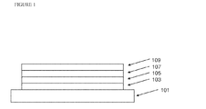
OLEDは、アノード103、りん光性発光層105、蛍光性発光層107およびカソード109を含む。蛍光性発光層107は、蛍光性発光材料およびTTAプロモータを含有する。OLEDは、基板101、例えばガラスまたはプラスチック基板上に支持される。光は、透明な基板101および透明なアノード103を通して発光されてもよく、または光は、透明なカソード109を通して発光されてもよく、この場合アノード103および基板101はそれぞれ、透明または半透明であってもよく、反射性であってもよい。
The OLED includes an
図1の実施形態において、蛍光性発光層107は、りん光性発光層105とカソードとの間にある。他の実施形態において、りん光性発光層105は、蛍光性発光層107とカソードとの間にあってもよい。
In the embodiment of FIG. 1, the fluorescent light-emitting
1つ以上のさらなる層が、アノード103とカソード109との間に位置してもよい。さらなる層は、さらなる発光層、電荷輸送層、電荷注入層および電荷ブロッキング層から選択されてもよい。
One or more additional layers may be located between the
例示的な発光構造は、以下を含む:
アノード/発光層/カソード
アノード/正孔注入層/発光層/カソード
アノード/正孔注入層/正孔輸送層/発光層/カソード
発光層は、りん光性層および隣接蛍光性発光層からなってもよく、または1つ以上のさらなる発光層を含有してもよい。さらなる発光層は、蛍光性またはりん光性発光層であってもよい。好ましくはデバイスは、2つまたは3つの発光層を含有する。1つの発光層は、異なるピーク波長の光を発光する2つの異なる発光材料を含有してもよい。
Exemplary light emitting structures include:
Anode / light-emitting layer / cathode anode / hole injection layer / light-emitting layer / cathode anode / hole injection layer / hole transport layer / light-emitting layer / cathode The light-emitting layer is composed of a phosphorescent layer and an adjacent fluorescent light-emitting layer. Or it may contain one or more additional light emitting layers. The further light emitting layer may be a fluorescent or phosphorescent light emitting layer. Preferably the device contains two or three light emitting layers. One light emitting layer may contain two different light emitting materials that emit light having different peak wavelengths.
好ましい実施形態において、発光層からの発光は、組み合わせて白色光を生じる。白色光は、青色および黄色光の組み合わせによって、または赤色、緑色および青色光の組み合わせによって得てもよい。例示的な発光層の組み合わせは以下が挙げられる:
緑色りん光性/赤色りん光性/青色蛍光性
赤色りん光性および緑色りん光性/青色蛍光性
黄色りん光性/青色蛍光性
黄色りん光性/赤色りん光性/青色蛍光性
青色発光材料は、400〜490nmの範囲にピークを有するフォトルミネッセンススペクトルを有していてもよい。
In a preferred embodiment, the light emission from the light emitting layer is combined to produce white light. White light may be obtained by a combination of blue and yellow light or by a combination of red, green and blue light. Exemplary light emitting layer combinations include the following:
Green phosphorescent / red phosphorescent / blue fluorescent red phosphorescent and green phosphorescent / blue fluorescent yellow phosphorescent / blue fluorescent yellow phosphorescent / red phosphorescent / blue fluorescent blue light emitting material May have a photoluminescence spectrum having a peak in the range of 400 to 490 nm.
緑色発光りん光性材料は、490〜560nmを超える範囲にピークを有するフォトルミネッセンススペクトルを有していてもよい。 The green light emitting phosphorescent material may have a photoluminescence spectrum having a peak in a range exceeding 490 to 560 nm.
黄色発光りん光性材料は、560〜590nmを超える範囲にピークを有するフォトルミネッセンススペクトルを有していてもよい。 The yellow light-emitting phosphorescent material may have a photoluminescence spectrum having a peak in a range exceeding 560 to 590 nm.
赤色発光りん光性材料は、約590〜700nm超過にてフォトルミネッセンス発光スペクトルのピークを有していてもよい。 The red-emitting phosphorescent material may have a photoluminescence emission spectrum peak at greater than about 590-700 nm.
白色発光OLEDは、単一の白色発光層を含有してもよく、または組み合わせて白色光を生じる異なる色を発光する2つ以上の層を含有してもよい。白色発光OLEDから発光される光は、2500〜9000Kの範囲の温度において黒体によって発光されるものと等価なCIEx座標、および黒体によって発光されるこの光のCIEy座標の0.05または0.025内のCIEy座標を有していてもよく、2600〜4500Kの範囲の温度において黒体によって発光されるものと等価なCIEx座標を有していてもよい。 White light emitting OLEDs may contain a single white light emitting layer or may contain two or more layers that emit different colors that combine to produce white light. The light emitted from the white light emitting OLED has a CIE x coordinate equivalent to that emitted by the black body at a temperature in the range of 2500 to 9000K, and a CIE y coordinate of this light emitted by the black body of 0.05 or 0.00. It may have CIEy coordinates within 025, and may have CIEx coordinates equivalent to those emitted by a black body at temperatures in the range of 2600-4500K.
各発光層は、約10〜100nmの範囲の厚さを有していてもよい。 Each light emitting layer may have a thickness in the range of about 10-100 nm.
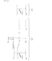
図2は、本発明の実施形態に従うOLEDのための第1のエネルギー移動機構を例示し、ここでOLEDは、OLEDの蛍光性発光層107において蛍光性発光材料、および三重項−三重項消滅(TTA)プロモータを含む。蛍光性発光材料およびTTAプロモータは、発光層において共にブレンドされる別個の材料であってもよい。あるいは、TTAプロモータは、発光材料に結合してもよい;例えば発光材料およびTTAプロモータは、発光繰り返しユニットおよびTTAプロモーティング繰り返しユニットを含む共役または非共役ポリマーの形態であってもよい。
FIG. 2 illustrates a first energy transfer mechanism for an OLED according to an embodiment of the present invention, wherein the OLED is a fluorescent light-emitting material and triplet-triplet annihilation (in the fluorescent light-emitting
操作中、それぞれエネルギー準位S1FおよびT1Fを有する一重項および三重項励起子は、蛍光性発光材料上で形成される。エネルギーS1Fを有する一重項励起子は、図2のS1FとS0Eとの間の実線矢印によって例示される蛍光性光hνの発光により減衰し得る。図1において点線矢印によって例示されるT1FからS0Fへの三重項励起子の減衰は、スピン禁制プロセスである。 During operation, singlet and triplet excitons having energy levels S 1F and T 1F , respectively, are formed on the fluorescent luminescent material. Singlet excitons having energy S 1F can be attenuated by the emission of fluorescent light hν illustrated by the solid line arrow between S 1F and S 0E in FIG. The decay of triplet excitons from T 1F to S 0F , exemplified by the dotted arrows in FIG. 1, is a spin-forbidden process.
T1Fにて形成された三重項励起子は、TTAプロモータの三重項励起された準位T1Tに移動し得る。T1Fより低いエネルギー準位T1Tを有するTTAプロモータを提供することによって、T1FからT1Tへの励起子の迅速な移動が生じ得る。この移動は、T1FからS0Fへの三重項励起子の減衰のスピン禁制プロセスに比べて相対的に迅速であり得る。 The triplet exciton formed at T 1F can move to the triplet excited level T 1T of the TTA promoter. By providing a TTA promoter with an energy level T 1T lower than T 1F , rapid exciton transfer from T 1F to T 1T can occur. This transfer can be relatively rapid compared to the spin-forbidden process of triplet exciton decay from T 1F to S 0F .
T1FとT1Tとの間のエネルギーギャップは、好ましくはT1TからT1Fへの励起子の逆移動を回避するためにkTより大きい。蛍光性材料の一重項励起された状態S1Fは、好ましくはTTAプロモータの一重項励起された状態のエネルギー準位S1Tよりも低い。S1TとS1Fとの間のエネルギーギャップは、好ましくはS1FからS1Tへの励起子の移動を回避するためにkTより大きい。 The energy gap between T 1F and T 1T is preferably larger than kT in order to avoid exciton back-migration from T 1T to T 1F . The singlet excited state S 1F of the fluorescent material is preferably lower than the energy level S 1T in the singlet excited state of the TTA promoter. The energy gap between S 1T and S 1F is preferably larger than kT to avoid exciton migration from S 1F to S 1T .
遅延蛍光を生じる三重項−三重項消滅(TTA)は、2つのTTAプロモータ間の相互作用によって生じ得るもので、結果として2×T1Tまでのエネルギーを有する三重項−三重項消滅された一重項励起子を形成する。2つの三重項プロモータユニットの第1のものに形成されたこの一重項励起子は、S1TおよびS1Fよりもエネルギーが高いエネルギー準位SnTを有し、そのためそれはS1Tへ、次いでS1Fへ移動でき、ここから光hν(F)は、遅延蛍光として発光され得る。 Triplet-triplet annihilation (TTA) resulting in delayed fluorescence can be caused by the interaction between two TTA promoters, resulting in triplet-triplet annihilated singlet with energy up to 2 × T 1T. Form excitons. This singlet exciton formed in the first of the two triplet promoter units has an energy level S nT that is higher in energy than S 1T and S 1F , so that it goes to S 1T and then S 1F From here, the light hν (F) can be emitted as delayed fluorescence.
三重項−三重項消滅と競合するT1Tの三重項励起子の減衰経路は、T1TおよびS0Tとの間の点線によって例示されるS0Tへの非放射性(消光)経路である。S0Tへの減衰よりもむしろTTAの確率を最大限にする多数の基準が採用され得る、特に:
i)TTAプロモータは、T1Tの三重項励起子が、相対的に長い寿命τを有するように、選択されてもよい。相対的に長い寿命は、S0Tへの減衰速度が相対的に遅いだけでなく、TTAの尤度が相対的に高いことを意味する。
Triplet - attenuation path triplet excitons T 1T to compete with triplet annihilation is a non-radioactive (quenching) route to S 0T exemplified by the dotted line between the T 1T and S 0T. A number of criteria that maximize the probability of TTA rather than decay to SOT can be employed, in particular:
i) The TTA promoter may be selected such that the T 1T triplet exciton has a relatively long lifetime τ. A relatively long lifetime means not only that the decay rate to SOT is relatively slow, but also that the likelihood of TTA is relatively high.
ii)2つ以上のTTAプロモータユニットは、極めて近位で提供され得る。 ii) Two or more TTA promoter units may be provided very proximally.
これらの基準のそれぞれは、単独でまたは組み合わせて使用されてもよい。 Each of these criteria may be used alone or in combination.
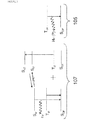
図3は、TTAプロモータに位置するエネルギーT1Tの三重項励起子と、蛍光性発光材料上に位置するエネルギーT1Fの三重項励起子との間で三重項−三重項消滅が生じる第2のエネルギー移動を例示する。これにより、T1F+T1Tまでのエネルギーを有する三重項−三重項消滅された一重項励起子がもたらされることが理解される。この一重項励起子は、S1Fよりもエネルギーが高く、S1Fへそのエネルギーを移動させる場合があり、ここから光hνは、遅延蛍光として発光され得る。 FIG. 3 shows a second example in which triplet-triplet annihilation occurs between triplet excitons with energy T 1T located on the TTA promoter and triplet excitons with energy T 1F located on the fluorescent light-emitting material. Illustrates energy transfer. It is understood that this results in triplet-triplet annihilated singlet excitons having energies up to T 1F + T 1T . The singlet excitons, higher energy than S 1F, may move the energy of S 1F navel, wherein the light hν can be emitted as delayed fluorescence.
図2および3において、エネルギー準位S1TはS1Eより大きいことが好ましい場合があるが、これは三重項吸収が生じるためには必須ではないことが理解される。 2 and 3, it may be preferred that the energy level S 1T is greater than S 1E , but it is understood that this is not essential for triplet absorption to occur.
TTAを生じ、安定に遅延蛍光を生じるためにTTAプロモータを利用することによって、TTAプロモータが存在しないデバイスに比べて、効率を改善できる。 Utilizing the TTA promoter to generate TTA and stably generate delayed fluorescence can improve efficiency compared to devices without the TTA promoter.
図2および3において、TTAは、それぞれTTAプロモータ−TTAプロモータ三重項消滅およびTTAプロモータ−蛍光性エミッタ材料三重項消滅機構に関して記載されているが、両方の機構は、同じデバイスで操作でき、これら2つの機構それぞれからの遅延蛍光の量は、蛍光性発光材料の濃度、TTAプロモータの濃度、発光ユニットおよびTTAプロモータユニットの三重項励起子の励起状態寿命のような因子に依存することが理解される。図2を参照して上記で記載された基準は、TTAの確率を増大させるために使用されてもよい。 In FIGS. 2 and 3, TTA is described with respect to the TTA promoter-TTA promoter triplet annihilation and TTA promoter-fluorescent emitter material triplet annihilation mechanisms, respectively, but both mechanisms can operate on the same device. It is understood that the amount of delayed fluorescence from each of the two mechanisms depends on factors such as the concentration of the fluorescent luminescent material, the concentration of the TTA promoter, the excited state lifetime of the triplet excitons of the luminescent unit and the TTA promoter unit. . The criteria described above with reference to FIG. 2 may be used to increase the probability of TTA.
蛍光性発光材料およびTTAプロモータは、蛍光性発光材料からTTAプロモータへの三重項励起子の移動の速度定数が、TTAプロモータによって三重項励起子の消光の速度定数よりも大きくなるように選択され得るように選択され得る。 The fluorescent luminescent material and the TTA promoter can be selected such that the rate constant of triplet exciton transfer from the fluorescent luminescent material to the TTA promoter is greater than the rate constant of quenching of the triplet exciton by the TTA promoter. Can be selected.
本発明のデバイスの蛍光性発光層から発光された光は、上記で記載されるように、遅延蛍光を含んでいてもよく、ならびに発光材料における正孔および電子の再結合から直接生じる蛍光(「即時蛍光」)を含んでいてもよい。 The light emitted from the fluorescent light-emitting layer of the device of the present invention may contain delayed fluorescence, as described above, and the fluorescence directly generated from the recombination of holes and electrons in the light-emitting material (“ "Immediate fluorescence").
当業者は、例えば即時蛍光が続く発光組成物からの光発光を測定することによって、発光組成物から発光された光の遅延蛍光の存在を決定するための方法を承知している。 Those skilled in the art are aware of methods for determining the presence of delayed fluorescence of light emitted from a luminescent composition, for example by measuring light emission from a luminescent composition followed by immediate fluorescence.
時間分解エレクトロルミネッセンススペクトルは、例示デバイスのターンオフの間に得てもよい;ここで電流のターンオフ後にTTAが生じ、デバイスのRC時間定数と同様の時間スケールでの輝度の初期の迅速減衰は、通常数マイクロ秒の期間での発光減衰において残留シグナルを生じる。一般に、OLED中の遅い遷移発光は、深いトラップまたは界面電荷層またはTTAからの電荷の再結合に起因する(Kondakov,D.Y.Characterization of triplet−triplet annihilation in organic light−emitting diodes based on anthracene derivatives.J.Appl.Phys.102,114504−5(2007)、Sinha,S.,Rothe,C.,Guentner,R.,Scherf,U.&Monkman,A.P.Electrophosphorescence and Delayed Electroluminescence from Pristine polyfluorene Thin Film Devices at Low Temperature.Physical Review Letters 90,127402(2003)およびSinha,S.,Monkman,A.P.,Guntner,R.&Scherf,U.Space−charge−mediated delayed Electroluminescence from polyfluorene thin films.Appl.Phys.Lett.82,4693−4695(2003)を参照のこと)。 A time-resolved electroluminescence spectrum may be obtained during turn-off of the exemplary device; here, TTA occurs after turn-off of the current, and the initial rapid decay of brightness on a time scale similar to the RC time constant of the device is usually A residual signal is produced in the emission decay over a period of several microseconds. In general, slow transition emission in OLEDs is due to deep traps or recombination of charges from the interfacial charge layer or TTA (Kondakov, DY Characteristic of triplet ani- tiative lightning-emittering emis- J. Appl. Phys. 102, 114504-5 (2007), Sinha, S., Rothe, C., Guentner, R., Scherf, U. & Monkman, A. P. Electrophosphorescence and Delayed Electroluminescence. ore Thin Film Devices at Low Temperature. Physical Review Letters 90, 127402 (2003) and Sinha, S., Monkman, A. P., Gunter, R. & Scherf, U. s. Appl. Phys. Lett. 82, 4673-4695 (2003)).
2つの機構を区別するために、同じ遷移エレクトロルミネッセンストレースを、デバイス電流のターンオフ後に10vリバースバイアスをパルス100nsで印加して測定されることができ、このパルスは、輝度の減衰に対する捕捉された電荷の寄与を除去、または少なくとも十分乱す。標準減衰形状に比べてリバースバイアスパルス後の輝度の減衰が変化していない場合、捕捉された電荷の再結合が、残留輝度シグナルに十分寄与せず、むしろTTAから生じる遅延蛍光によると結論付けられ得る(Popovic,Z.D.&Aziz,H.Delayed electroluminescence in small−molecule−based organic light−emitting diodes:Evidence for triplet−triplet annihilation and recombination−center−mediated light−generation mechanism.J.Appl.Phys.98,013510−5(2005))。 To distinguish between the two mechanisms, the same transition electroluminescence trace can be measured with a 10 v reverse bias applied at a pulse of 100 ns after device current turn-off, which pulse captures charge against luminance decay. Remove the contribution of, or at least disturb enough. If the luminance decay after the reverse bias pulse has not changed compared to the standard decay shape, it can be concluded that the recombination of the trapped charge does not contribute well to the residual luminance signal, but rather due to delayed fluorescence resulting from TTA. get (Popovic, Z.D & Aziz, H.Delayed electroluminescence in small-molecule-based organic light-emitting diodes:. Evidence for triplet-triplet annihilation and recombination-center-mediated light-generation mechanism.J.Appl.Phys.98 , 013510-5 (2005)).
蛍光性発光層107に隣接するりん光性発光層105は、図2および3に示されるように、三重項励起された状態のエネルギー準位T1Pを有するりん光性発光材料を含有する。りん光性発光材料は、T1Pから基底状態S0Pへの三重項励起子の減衰によって、りん光性発光hν(P)を生じることができる。T1Pエネルギー準位は、隣接蛍光性発光層105におけるT1Tよりも大きくてもよい。
As shown in FIGS. 2 and 3, the phosphorescent light-emitting
蛍光性発光材料のT1Fエネルギー準位は、層105のりん光性材料のT1Pエネルギー準位より0.1eV以下で低く、層105のりん光性材料のT1Pエネルギー準位と同じまたはそれより高くてもよい。
The T 1F energy level of the fluorescent light emitting material is lower than the T 1P energy level of the phosphorescent material of the
三重項エネルギー準位は、低温りん光分光法によって測定され得る(Y.V.Romaovskii et al,Physical Review Letters,2000,85(5),p1027,A.van Dijken et al,Journal of the American Chemical Society,2004,126,p7718)。 Triplet energy levels can be measured by low-temperature phosphorescence spectroscopy (YV Romanovskii et al, Physical Review Letters, 2000, 85 (5), p1027, A. van Dijken et al, Journal of the American. Society, 2004, 126, p7718).
一重項エネルギー準位は、蛍光分光法によって測定され得る。 Singlet energy levels can be measured by fluorescence spectroscopy.
蛍光性発光材料
好適な蛍光性発光材料としては、小分子、ポリマー性およびデンドリマー性材料、ならびにこれらの組成物が挙げられる。好適な発光ポリマーとしては、ポリ(アリーレンビニレン)、例えばポリ(p−フェニレンビニレン)およびポリアリーレン、例えば:ポリフルオレン、特に2,7−連結された9,9ジアルキルポリフルオレンまたは2,7−連結された9,9ジアリールポリフルオレン;ポリスピロフルオレン、特に2,7−連結されたポリ−9,9−スピロフルオレン;ポリインデノフルオレン、特に2,7−連結されたポリインデノフルオレン;ポリフェニレン、特にアルキルまたはアルコキシ置換されたポリ−1,4−フェニレンが挙げられる。こうしたポリマーは、例えばAdv.Mater.2000 12(23)1737−1750およびその中の参照文献に開示される。
Fluorescent luminescent materials Suitable fluorescent luminescent materials include small molecules, polymeric and dendrimeric materials, and compositions thereof. Suitable light-emitting polymers include poly (arylene vinylenes) such as poly (p-phenylene vinylene) and polyarylenes such as: polyfluorene, especially 2,7-linked 9,9 dialkyl polyfluorene or 2,7-linked 9,9 diarylpolyfluorenes; polyspirofluorenes, in particular 2,7-linked poly-9,9-spirofluorenes; polyindenofluorenes, in particular 2,7-linked polyindenofluorenes; In particular, alkyl-1, alkoxy-substituted poly-1,4-phenylene. Such polymers are described, for example, in Adv. Mater. 2000 12 (23) 1737-1750 and references therein.
蛍光性発光材料は、好ましくは、480nm以下、例えば400〜480nmの範囲のピークフォトルミネッセンス波長を有する青色蛍光性材料である。 The fluorescent light-emitting material is preferably a blue fluorescent material having a peak photoluminescence wavelength in the range of 480 nm or less, such as 400-480 nm.
蛍光性発光ポリマーは、発光繰り返しユニットを含む発光ホモポリマーであってもよく、またはそれは、例えば国際公開第00/55927号に開示されるような発光繰り返しユニットおよびさらなる繰り返しユニット、例えば正孔輸送および/または電子輸送繰り返しユニットを含むコポリマーであってもよい。各繰り返しユニットは、ポリマーの主鎖または側鎖に提供されてもよい。 The fluorescent light-emitting polymer may be a light-emitting homopolymer comprising a light-emitting repeating unit, or it may be a light-emitting repeating unit and further repeating units such as disclosed in WO 00/55927, for example hole transport and It may also be a copolymer comprising electron transport repeat units. Each repeating unit may be provided in the main chain or side chain of the polymer.
蛍光性発光ポリマーは、非共役骨格からのペンダント共役基を有する非共役骨格を有していてもよく、または互いに共役した繰り返しユニットを含有する骨格を有するポリマーであってもよい。 The fluorescent light-emitting polymer may have a non-conjugated skeleton having a pendant conjugated group from the non-conjugated skeleton, or may be a polymer having a skeleton containing repeating units conjugated to each other.
共役蛍光性発光ホモポリマーまたはコポリマーの例示的な繰り返しユニットは、1つ以上のアリーレン、ヘテロアリーレン、ビニレンおよびアリーレンビニレン(例えばフェニレンビニレン)およびアリールアミン繰り返しユニットを含んでいてもよい。各繰り返しユニットは、非置換または1つ以上の置換基で置換されてもよい。存在する場合、置換基は、C1−40ヒドロカルビル基から選択されてもよい。 Exemplary repeating units of a conjugated fluorescent light emitting homopolymer or copolymer may include one or more arylene, heteroarylene, vinylene and arylene vinylene (eg, phenylene vinylene) and arylamine repeating units. Each repeating unit may be unsubstituted or substituted with one or more substituents. When present, the substituent may be selected from a C 1-40 hydrocarbyl group.
共役ポリマーは、好ましくは、隣接繰り返しユニットのアリーレンまたはヘテロアリーレン基と共役するアリーレンまたはヘテロアリーレン基を有する繰り返しユニットを含む。繰り返しユニットにわたる共役程度、すなわち繰り返しユニットと繰り返しユニットの両側の隣接繰り返しユニットとの間の共役度は、例えば一重項および/または三重項エネルギー準位を制御するために、制御されてもよい。 The conjugated polymer preferably comprises a repeating unit having an arylene or heteroarylene group that is conjugated with an arylene or heteroarylene group of an adjacent repeating unit. The degree of conjugation across the repeating unit, ie the degree of conjugation between the repeating unit and the adjacent repeating units on either side of the repeating unit, may be controlled, for example, to control singlet and / or triplet energy levels.
例示的なフルオレン繰り返しユニットは以下の式(I)を有する:
式中、R5は、各出現時において、同一または異なり、Hまたは置換基であり、2つの基R5は、連結して環を形成してもよい。 In the formula, R 5 is the same or different at each occurrence and is H or a substituent, and the two groups R 5 may be linked to form a ring.
各R5は、好ましくは置換基であり、各R5は、独立に、以下からなる群から選択されてもよい:
置換または非置換アルキル(C1−20アルキルであってもよい)であって、ここで1つ以上の非隣接C原子は、置換されてもよいアリールまたはヘテロアリール、O、S、置換されたN、C=Oまたは−COO−で置き換えられてもよく、1つ以上のH原子はFで置き換えられてもよいアルキル;
置換または非置換アリールまたはヘテロアリール基、または線状または分岐鎖状のアリールまたはヘテロアリール基であって、そのそれぞれは、独立に、例えば式−(Ar4)rの基で置換されてもよく、ここでAr4は、各出現時において、独立に、置換または非置換アリールまたはヘテロアリール基であり、rは少なくとも1であり、1、2または3であってもよいアリールまたはヘテロアリール基;
フルオレンユニットに直接結合した、またはスペーサ基、例えば二重結合を含む基、例えばビニルまたはアクリレート基、またはベンゾシクロブタン基によってそこから間隔をあけられた架橋性基。
Each R 5 is preferably a substituent, and each R 5 may be independently selected from the group consisting of:
Substituted or unsubstituted alkyl (which may be C 1-20 alkyl), wherein one or more non-adjacent C atoms are optionally substituted aryl or heteroaryl, O, S, substituted N, C═O or —COO—, wherein one or more H atoms may be replaced with F alkyl;
A substituted or unsubstituted aryl or heteroaryl group, or a linear or branched aryl or heteroaryl group, each of which may independently be substituted, for example, with a group of formula — (Ar 4 ) r Where Ar 4 is independently at each occurrence a substituted or unsubstituted aryl or heteroaryl group, r is at least 1 and may be 1, 2 or 3, an aryl or heteroaryl group;
Crosslinkable groups bonded directly to the fluorene unit or spaced therefrom by a spacer group, such as a group containing a double bond, such as a vinyl or acrylate group, or a benzocyclobutane group.
R5が1つ以上のアリールまたはヘテロアリール基Ar4を含む場合、各Ar4は、独立に、以下からなる群から選択される1つ以上の置換基R6で置換されてもよい:
アルキル、例えばC1−20アルキルであって、ここで1つ以上の非隣接C原子は、O、S、置換されたN、C=Oおよび−COO−で置き換えられてもよく、アルキル基の1つ以上のH原子はFまたは1つ以上の基R7で置換されてもよいアリールまたはヘテロアリールで置き換えられてもよいアルキル、
1つ以上の基R7で置換されてもよいアリールまたはヘテロアリール、
NR8 2、OR8、SR8、および
フッ素、ニトロおよびシアノ、
ここで各R7は、独立に、アルキル、例えばC1−20アルキルであって、ここで1つ以上の非隣接C原子は、O、S、置換されたN、C=Oまたは−COO−で置き換えられてもよく、アルキル基の1つ以上のH原子はFまたはDで置換されてもよく;各R8は、独立に、アルキル、例えばC1−20アルキル、1つ以上のアルキル基で置換されてもよいアリールまたはヘテロアリール、例えば非置換または1つ以上のC1−20アルキル基で置換されたフェニルからなる群から選択される。
When R 5 includes one or more aryl or heteroaryl groups Ar 4 , each Ar 4 may be independently substituted with one or more substituents R 6 selected from the group consisting of:
Alkyl, such as C 1-20 alkyl, wherein one or more non-adjacent C atoms may be replaced by O, S, substituted N, C═O and —COO— One or more H atoms may be substituted with aryl or heteroaryl, which may be substituted with F or one or more groups R 7 ,
Aryl or heteroaryl optionally substituted by one or more groups R 7 ,
NR 8 2 , OR 8 , SR 8 , and fluorine, nitro and cyano,
Wherein each R 7 is independently alkyl, eg, C 1-20 alkyl, wherein one or more non-adjacent C atoms are O, S, substituted N, C═O or —COO— And one or more H atoms of the alkyl group may be substituted with F or D; each R 8 is independently alkyl, eg, C 1-20 alkyl, one or more alkyl groups Selected from the group consisting of aryl or heteroaryl optionally substituted with, for example, phenyl, unsubstituted or substituted with one or more C 1-20 alkyl groups.
フルオレン繰り返しユニットの芳香族炭素原子はすべて非置換であってもよく、またはこれらの芳香族炭素原子の1つ以上は、置換基R4で置換されてもよい。存在する場合、各R4は、独立に、アルキル、例えばC1−20アルキル(ここで1つ以上の非隣接C原子は、O、S、NH、または置換されたN、C=Oおよび−COO−で置き換えられてもよい)、置換されてもよいアリール、置換されてもよいヘテロアリール、アルコキシ、アルキルチオ、フッ素、シアノおよびアリールアルキルからなる群から選択される。特に好ましい置換基R4としては、C1−20アルキルおよび置換または非置換アリール、例えばフェニルが挙げられる。アリールのための任意の置換基としては、1つ以上のC1−20アルキル基が挙げられる。 All of the aromatic carbon atoms of the fluorene repeat unit may be unsubstituted, or one or more of these aromatic carbon atoms may be substituted with the substituent R 4 . When present, each R 4 is independently alkyl, such as C 1-20 alkyl (where one or more non-adjacent C atoms are O, S, NH, or substituted N, C═O and — Selected from the group consisting of optionally substituted aryl, optionally substituted heteroaryl, alkoxy, alkylthio, fluorine, cyano and arylalkyl. Particularly preferred substituents R 4 include C 1-20 alkyl and substituted or unsubstituted aryl such as phenyl. Optional substituents for aryl include one or more C 1-20 alkyl groups.
存在する場合、置換されたNは、独立に、各出現時において、NR9であってもよく、ここでR9は、アルキル(C1−20アルキルであってもよい)、または置換されてもよいアリールまたはヘテロアリールである。アリールまたはヘテロアリールのための任意の置換基R9は、R7またはR8から選択されてもよい。 When present, substituted N may independently be NR 9 at each occurrence, where R 9 is alkyl (which may be C 1-20 alkyl), or substituted. May be aryl or heteroaryl. The optional substituent R 9 for aryl or heteroaryl may be selected from R 7 or R 8 .
好ましくは、各R5は、C1−20アルキルおよび−(Ar4)rからなる群から選択され、ここでAr4は、各出現時において、置換または非置換の置換されたフェニルである。フェニルのための任意の置換基としては、1つ以上のC1−20アルキル基が挙げられる。 Preferably, each R 5 is selected from the group consisting of C 1-20 alkyl and — (Ar 4 ) r , wherein Ar 4 is a substituted or unsubstituted substituted phenyl at each occurrence. Optional substituents for phenyl include one or more C 1-20 alkyl groups.
式(I)の繰り返しユニットは、式(Ia)の2,7−連結された繰り返しユニットであってもよい:
式(Ia)の繰り返しユニットは、2−または7−位に隣接する位置において置換基R4によって置換されなくてもよい。 The repeating unit of formula (Ia) may not be substituted by the substituent R 4 at a position adjacent to the 2- or 7-position.
隣接繰り返しユニットに対する式(I)の繰り返しユニットの共役度は、隣接繰り返しユニット、例えばC1−20アルキル置換基を3−および6−位の1つまたは両方に保持する2,7−連結されたフルオレンとツイストを創出するために、(a)繰り返しユニットを、3−および/または6−位置を通して連結して、繰り返しユニットにわたる共役度を制限すること、および/または(b)繰り返しユニットを、1つ以上のさらなる置換基R4で、連結位置に隣接する以上の位置で置換することによって、制限されてもよい。 The degree of conjugation of the repeating unit of formula (I) to the adjacent repeating unit is 2,7-linked holding an adjacent repeating unit, for example a C 1-20 alkyl substituent in one or both of the 3- and 6-position To create fluorene and twist, (a) repeating units are linked through 3- and / or 6-positions to limit the degree of conjugation across repeating units, and / or (b) repeating units 1 One or more further substituents R 4 may be limited by substitution at more positions adjacent to the linking position.
例示的なフェニレン含有繰り返しユニットは、以下の式(II)を有する:
式中、pは、0、1、2、3または4であり(1または2であってもよい);qは、1、2または3であり;R10は、独立に、各出現時において、置換基(式(I)を参照して上記で記載されたような置換基R5であってもよい)、例えばC1−20アルキル、および非置換または1つ以上のC1−20アルキル基で置換されたフェニルである。 Where p is 0, 1, 2, 3 or 4 (may be 1 or 2); q is 1, 2 or 3; R 10 is independently at each occurrence , A substituent (which may be a substituent R 5 as described above with reference to formula (I)), such as C 1-20 alkyl, and unsubstituted or one or more C 1-20 alkyl Phenyl substituted with a group.
q=1の場合、式(II)の繰り返しユニットは、1,4−連結、1,2−連結または1,3−連結であってもよい。 When q = 1, the repeating unit of formula (II) may be 1,4-linked, 1,2-linked or 1,3-linked.
式(II)の繰り返しユニットが1,4−連結されている場合、およびpが0である場合、式(II)の繰り返しユニットの共役度は、相対的に高くなり得る。 When the repeating units of formula (II) are 1,4-linked and when p is 0, the degree of conjugation of the repeating units of formula (II) can be relatively high.
pが少なくとも1であり、および/または繰り返しユニットが1,2−または1,3−連結される場合、式(II)の繰り返しユニットの共役度は、相対的に低くなり得る。1つの任意の配置において、q=1、式(II)の繰り返しユニットは、1,3−連結され、pは0、1、2または3である。別の任意の配置において、式(II)の繰り返しユニットは、以下の式(IIa)を有する:
別の例示的なアリーレン繰り返しユニットは以下の式(III)を有する:
式中、R5は、上記式(I)を参照して記載される通りである。R5基のそれぞれは、いずれかの他のR5基と連結して、環を形成してもよい。 Wherein R 5 is as described with reference to formula (I) above. Each of R 5 groups, in conjunction with any other R 5 groups may form a ring.
さらなるアリーレン共繰り返しユニットとしては:フェナントレン繰り返しユニット;ナフタレン繰り返しユニット;アントラセン繰り返しユニット;およびペリーレン繰り返しユニットが挙げられる。これらのアリーレン繰り返しユニットのそれぞれは、これらのユニットの芳香族炭素原子のいずれか2つを通して隣接繰り返しユニットに連結してもよい。具体的な例示連結としては、9,10−アントラセン;2,6−アントラセン;1,4−ナフタレン;2,6−ナフタレン;2,7−フェナントレン;および2,5−ペリーレンが挙げられる。これらの繰り返しユニットのそれぞれは、非置換または1つ以上の置換基で置換されてもよい。好ましい置換基は、C1−40ヒドロカルビル、例えばC1−20アルキル、および非置換または1つ以上のC1−20アルキル基で置換されたフェニルから選択される。 Additional arylene co-repeat units include: phenanthrene repeat units; naphthalene repeat units; anthracene repeat units; and perylene repeat units. Each of these arylene repeat units may be linked to an adjacent repeat unit through any two of the aromatic carbon atoms of these units. Specific exemplary linkages include 9,10-anthracene; 2,6-anthracene; 1,4-naphthalene; 2,6-naphthalene; 2,7-phenanthrene; and 2,5-perylene. Each of these repeating units may be unsubstituted or substituted with one or more substituents. Preferred substituents are selected from C 1-40 hydrocarbyl, such as C 1-20 alkyl, and phenyl which is unsubstituted or substituted with one or more C 1-20 alkyl groups.
ポリマーは、アミン繰り返しユニット、特に以下の式(IV)のアミンを含有してもよい:
式中、Ar8およびAr9は、各出現時において、独立に、置換または非置換アリールまたはヘテロアリールから選択され、gは、1以上、好ましくは1または2であり、R13は、Hまたは置換基、好ましくは置換基であり、cおよびdは、それぞれ独立に1、2または3である。 Wherein Ar 8 and Ar 9 are independently selected at each occurrence from substituted or unsubstituted aryl or heteroaryl, g is 1 or more, preferably 1 or 2, and R 13 is H or A substituent, preferably a substituent, and c and d are each independently 1, 2 or 3.
各出現時において、同一または異なっていてもよいR13は、g>1である場合、好ましくはアルキル、例えばC1−20アルキル、Ar10、分岐鎖または線状鎖のAr10基、または式(IV)のN原子に直接結合するまたはスペーサ基によってそこから間隔をあけた架橋性ユニットからなる群から選択され、ここでAr10は、各出現時において、独立に、置換されてもよいアリールまたはヘテロアリールである。例示的なスペーサ基は、C1−20アルキル、フェニルおよびフェニル−C1−20アルキルである。 R 13 , which may be the same or different at each occurrence, are preferably alkyl, for example C 1-20 alkyl, Ar 10 , branched or linear Ar 10 groups, or a formula, when g> 1 Selected from the group consisting of bridging units bonded directly to the N atom of (IV) or spaced therefrom by a spacer group, wherein Ar 10 is independently at each occurrence an optionally substituted aryl Or it is heteroaryl. Exemplary spacer groups are C 1-20 alkyl, phenyl and phenyl-C 1-20 alkyl.
式(IV)の繰り返しユニットにおいてAr8、Ar9および存在する場合Ar10のいずれかは、Ar8、Ar9およびAr10の別の基に、直接結合によってまたは二価の連結原子または基によって連結されてもよい。好ましい二価連結原子および基としては、O、S;置換されたN;および置換されたCが挙げられる。 Ar 8 , Ar 9 and any Ar 10 in the repeat unit of formula (IV) is bonded to another group of Ar 8 , Ar 9 and Ar 10 by a direct bond or by a divalent linking atom or group. It may be connected. Preferred divalent linking atoms and groups include O, S; substituted N; and substituted C.
Ar8、Ar9および存在する場合はAr10のいずれかは、1つ以上の置換基で置換されてもよい。例示的な置換基は、置換基R14であり、ここで各R14は、独立に、以下からなる群から選択されてもよい:
置換または非置換アルキル(C1−20アルキルであってもよい)、ここで1つ以上の非隣接C原子は、置換されてもよいアリールまたはヘテロアリール、O、S、置換されたN、C=Oまたは−COO−で置き換えられてもよく、1つ以上のH原子はFで置き換えられてもよいアルキル;および
Ar8、Ar9またはAr10に直接結合した、またはスペーサ基、例えば二重結合を含む基、例えばビニルまたはアクリレート基、またはベンゾシクロブタン基によってそこから間隔をあけられた架橋性基。
Any of Ar 8 , Ar 9 and Ar 10 , if present, may be substituted with one or more substituents. An exemplary substituent is substituent R 14 , where each R 14 may be independently selected from the group consisting of:
Substituted or unsubstituted alkyl (which may be C 1-20 alkyl), wherein one or more non-adjacent C atoms are optionally substituted aryl or heteroaryl, O, S, substituted N, C ═O or —COO—, wherein one or more H atoms may be replaced by F alkyl; and Ar 8 , Ar 9 or Ar 10 bonded directly or a spacer group, eg double Crosslinkable groups spaced therefrom by groups containing bonds, such as vinyl or acrylate groups, or benzocyclobutane groups.
存在する場合、置換されたNは、ヒドロカルビル基、例えばC1−10アルキル、非置換フェニルまたは1つ以上のC1−10アルキル基で置換されたフェニルで置換されたNであってもよい。 When present, substituted N may be a hydrocarbyl group, such as N substituted with a phenyl substituted with a C 1-10 alkyl, unsubstituted phenyl or one or more C 1-10 alkyl groups.
式(IV)の好ましい繰り返しユニットは、以下の式1〜3を有する:
1つの好ましい配置において、R13はAr10であり、Ar8、Ar9およびAr10のそれぞれは、独立に、1つ以上のC1−20アルキル基で置換されてもよい。 In one preferred arrangement, R 13 is Ar 10 and each of Ar 8 , Ar 9 and Ar 10 may independently be substituted with one or more C 1-20 alkyl groups.
Ar8、Ar9およびAr10は、好ましくはフェニルであり、そのそれぞれは独立に、上記で記載されるような1つ以上の置換基で置換されてもよい。 Ar 8 , Ar 9 and Ar 10 are preferably phenyl, each of which may independently be substituted with one or more substituents as described above.
別の好ましい配置において、Ar8およびAr9はフェニルであり、そのそれぞれは1つ以上のC1−20アルキル基で置換されてもよく、R13は、3,5−ジフェニルベンゼンであり、ここで各フェニルは、1つ以上のC1−20アルキル基で置換されてもよい。 In another preferred arrangement, Ar 8 and Ar 9 are phenyl, each of which may be substituted with one or more C 1-20 alkyl groups, and R 13 is 3,5-diphenylbenzene, wherein Each phenyl may be substituted with one or more C 1-20 alkyl groups.
別の好ましい配置において、c、dおよびgはそれぞれ1であり、Ar8およびAr9は、フェノキサジン環を形成するために酸素原子によって連結されるフェニルである。 In another preferred arrangement, c, d and g are each 1 and Ar 8 and Ar 9 are phenyl linked by an oxygen atom to form a phenoxazine ring.
アミン繰り返しユニットは、約0.5mol%から約50mol%までの範囲(約1〜25mol%、約1〜10mol%であってもよい)のモル量で提供されてもよい。 The amine repeat unit may be provided in a molar amount ranging from about 0.5 mol% to about 50 mol% (about 1-25 mol%, may be about 1-10 mol%).
式(IV)の繰り返しユニットは、正孔輸送および/または発光特性を提供してもよい。共役ポリマーは、1つ、2つ以上の式(IV)の異なる繰り返しユニット、例えば正孔輸送を提供するために式(IV)の第1の繰り返しユニット、および発光を提供するために式(IV)の第2の繰り返しユニットを含有してもよい。 The repeating unit of formula (IV) may provide hole transport and / or luminescent properties. The conjugated polymer is one, two or more different repeating units of formula (IV), such as a first repeating unit of formula (IV) to provide hole transport, and formula (IV) to provide light emission. ) Of the second repeating unit.
蛍光性発光コポリマーは、発光繰り返しユニットと、正孔輸送を提供するための繰り返しユニット、および電子輸送を提供するための繰り返しユニットのうちの少なくとも1つとを含んでいてもよい。式(IV)のアミン繰り返しユニットは、発光および正孔輸送を提供してもよい。電子輸送は、アリーレン繰り返しユニットの共役鎖、例えば式(I)のフルオレン繰り返しユニットの共役鎖によって提供されてもよい。 The fluorescent light emitting copolymer may comprise a light emitting repeating unit, at least one of a repeating unit for providing hole transport, and a repeating unit for providing electron transport. The amine repeat unit of formula (IV) may provide light emission and hole transport. Electron transport may be provided by a conjugated chain of an arylene repeat unit, such as a conjugated chain of a fluorene repeat unit of formula (I).
蛍光性発光層は、発光ポリマーおよびTTAプロモータだけからなってもよく、または1つ以上のさらなる材料と組み合わせてこれらの材料を含んでいてもよい。例えば発光ポリマーは、正孔および/または電子輸送材料とブレンドされてもよく、または別の方法として例えば国際公開第99/48160号に開示されるように、正孔および/または電子輸送材料に共有結合させてもよい。 The fluorescent light-emitting layer may consist solely of the light-emitting polymer and the TTA promoter, or may contain these materials in combination with one or more additional materials. For example, the light-emitting polymer may be blended with a hole and / or electron transport material, or alternatively shared with the hole and / or electron transport material, as disclosed, for example, in WO 99/48160. It may be combined.
TTAプロモータ
TTAプロモータは、蛍光性発光材料と化学的に結合しないが、物理的には混合される化合物であってもよい。さらなる材料、例えば1つ以上の電荷輸送材料(例えば正孔輸送および電子輸送材料の1つまたは両方)がまた蛍光性発光層に存在してもよい。あるいはTTAプロモータユニットは、発光材料または組成物の別の構成成分に、直接またはスペーサ基を通して結合、特に共有結合してもよい。
TTA promoter The TTA promoter may be a compound that does not chemically bind to the fluorescent luminescent material but is physically mixed. Additional materials, such as one or more charge transport materials (eg, one or both of hole transport and electron transport materials) may also be present in the fluorescent light-emitting layer. Alternatively, the TTA promoter unit may be bound, especially covalently bound, directly or through a spacer group to another component of the luminescent material or composition.
発光材料が、発光繰り返しユニットおよびさらなる繰り返しユニット、例えば式(IV)の発光アミン繰り返しユニットおよびアリーレン繰り返しユニット、例えば式(I)または(II)の繰り返しユニットを含む共役ポリマーである場合、TTAプロモータのポリマー主鎖への共役(例えばフルオレン繰り返しユニットとの共役)は、TTAプロモータのT1エネルギー準位を低下させる場合があるので、エミッタユニットからTTAプロモータユニットへの三重項励起子移動のエネルギーの優先性を増大させる。TTAプロモータのT1エネルギー準位のこうした低下はまた、このようにして共役していないTTAプロモータと共に使用するには低過ぎるT1準位を有する発光材料と共にTTAプロモータを使用できる。 When the luminescent material is a conjugated polymer comprising a luminescent repeat unit and a further repeat unit, such as a luminescent amine repeat unit of formula (IV) and an arylene repeat unit, such as a repeat unit of formula (I) or (II), Conjugation to the polymer backbone (eg, conjugation with a fluorene repeat unit) may reduce the T 1 energy level of the TTA promoter, thus giving priority to the energy of triplet exciton transfer from the emitter unit to the TTA promoter unit. Increase sex. Such a decrease in the T 1 energy level of the TTA promoter can also be used with a luminescent material that has a T 1 level that is too low for use with a TTA promoter that is thus unconjugated.
TTAプロモータが発光材料とブレンドされる場合、TTAプロモータは、小分子化合物またはポリマーであってもよい。 When a TTA promoter is blended with a luminescent material, the TTA promoter may be a small molecule compound or polymer.
有機化合物のS1およびT1エネルギー準位は、例えばDekker,Handbook of Photophysics 2nd Edition(1993)に開示される。所与の蛍光性発光材料と共に使用するのに好適なTTAプロモータは、これらの有機化合物の列挙されたS1およびT1エネルギー準位に基づいて選択されてもよい。 The S 1 and T 1 energy levels of organic compounds are disclosed, for example, in Dekker, Handbook of Photophysics 2nd Edition (1993). Suitable TTA promoters for use with a given fluorescent luminescent material may be selected based on the listed S 1 and T 1 energy levels of these organic compounds.
例示的なTTAプロモータ化合物としては、1つ以上の単環式または多環式環を含む芳香族またはヘテロ芳香族化合物(1つ以上のアルケニルまたはアルキニル基を含んでいてもよい)、例えば多環芳香族炭化水素、例えばアントラセン、ペリーレンおよびアンタントレンおよびそれらの誘導体;ジスチリルアリールおよびそれらの誘導体、例えばジスチリルベンゼン、ジスチリルビフェニル、スチルベン、フルベン、ジベンゾフルベン、線状ポリエン(2から6アルケン)(シクロオクタテトラエンのような環状ポリエンを含む)が挙げられる。 Exemplary TTA promoter compounds include aromatic or heteroaromatic compounds (which may contain one or more alkenyl or alkynyl groups) containing one or more monocyclic or polycyclic rings, such as polycyclic Aromatic hydrocarbons such as anthracene, perylene and anthanthrene and their derivatives; distyrylaryl and their derivatives such as distyrylbenzene, distyrylbiphenyl, stilbene, fulvene, dibenzofulvene, linear polyenes (2 to 6 alkenes) (Including cyclic polyenes such as cyclooctatetraene).
これらの化合物のいずれかは、置換されてもよく、例えば1つ以上の可溶化基、例えばC1−20アルキルで置換されてもよく、例えばポリマーの繰り返しユニットとしてより大きい構造の構成成分として提供されてもよい。 Any of these compounds may be substituted, eg, substituted with one or more solubilizing groups, eg, C 1-20 alkyl, and provided, for example, as a structural component of a larger structure as a repeating unit of the polymer May be.
適切な一重項および三重項光物理特性を有するさらなる材料は、その内容が参考として本明細書に組み込まれるHandbook of Photochemistry,2nd Edition,Steven L Murov,Ian Carmichael and Gordon L Hugに記載されており、それら化合物のそれぞれは、置換されていてもよく、例えばアルキル基で置換されていてもよい。 Additional materials having suitable singlet and triplet light physical properties, Handbook of Photochemistry, the contents of which are incorporated herein by reference, 2 nd Edition, Steven L Murov , are described in Ian Carmichael and Gordon L Hug Each of these compounds may be substituted, for example, may be substituted with an alkyl group.
発光材料とブレンドされるTTAプロモータポリマー、または蛍光性発光材料の繰り返しユニットおよびTTAプロモータを含有するポリマーは、好ましくは以下の式(V)の繰り返しユニットを含有する:
式中、PAHは、非置換または1つ以上の置換基で置換されてもよい多環芳香族炭化水素を表す。特に好ましい置換基は、C1−40ヒドロカルビル、好ましくはC1−20アルキルから選択される。ヒドロカルビル置換基、例えばアルキル置換基は、非極性有機溶媒、例えばモノ−およびポリ−アルキル化ベンゼン中への溶解度を提供し得る。
The TTA promoter polymer blended with the luminescent material or the repeating unit of fluorescent luminescent material and the polymer containing the TTA promoter preferably contains the following repeating unit of formula (V):
In the formula, PAH represents a polycyclic aromatic hydrocarbon which may be unsubstituted or substituted with one or more substituents. Particularly preferred substituents are selected from C 1-40 hydrocarbyl, preferably C 1-20 alkyl. Hydrocarbyl substituents, such as alkyl substituents, can provide solubility in nonpolar organic solvents, such as mono- and poly-alkylated benzenes.
例示的な多環芳香族炭化水素PAHとしては、アントラセン、ペリーレンおよびアンタントレンが挙げられる。 Exemplary polycyclic aromatic hydrocarbons PAH include anthracene, perylene and anthanthrene.
発光材料とブレンドされるTTAプロモータポリマーは、式(V)の繰り返しユニットおよび1つ以上の共繰り返しユニットを含有してもよい。例示的な共繰り返しユニットとしては、式(I)のフルオレン繰り返しユニットおよび式(II)のフェニレン繰り返しユニットが挙げられる。 The TTA promoter polymer blended with the luminescent material may contain a repeating unit of formula (V) and one or more co-repeating units. Exemplary co-repeat units include fluorene repeat units of formula (I) and phenylene repeat units of formula (II).
特に好ましい多環芳香族繰り返しユニットは、式(Va)のアントラセンである:
A particularly preferred polycyclic aromatic repeat unit is an anthracene of formula (Va):
アントラセン繰り返しユニットは、非置換または例えば1つ以上のC1−20アルキル基で置換されてもよい。 Anthracene repeat units may be unsubstituted or substituted, for example, with one or more C 1-20 alkyl groups.
TTAプロモータは、ポリマーの末端基または側鎖基として提供されてもよい。 The TTA promoter may be provided as a polymer end group or side chain group.
側鎖基は、以下に例示されるようなモノマーの置換基としてそれを提供することによって発光ポリマーに組み込まれてもよい:
式中、PGは、重合性基、例えば上記で記載されるような脱離基または重合性二重結合を表す。重合性ユニットは、芳香族またはヘテロ芳香族ユニット、例えば式(I)または(II)のフルオレンまたはフェニレンユニットであってもよく、TTAプロモータユニットは、重合性ユニットに直接結合されてもよく、またはスペーサ鎖、例えば1つ以上の非隣接C原子がOで置き換えられてもよいC1−20アルキル鎖によって間隔をあけられてもよい。 In the formula, PG represents a polymerizable group, for example a leaving group or a polymerizable double bond as described above. The polymerizable unit may be an aromatic or heteroaromatic unit, such as a fluorene or phenylene unit of formula (I) or (II), the TTA promoter unit may be directly bonded to the polymerizable unit, or It may be spaced by a spacer chain, for example a C 1-20 alkyl chain in which one or more non-adjacent C atoms may be replaced by O.
上記で記載されるようにTTAの確率および遅延蛍光を増大させるために、TTAプロモータは、極めて近位で提供される複数のTTAプロモータユニットを含有してもよい。例えば2つのこうしたユニットは、以下の一般式(VI)を有する置換されてもよい材料において提供されてもよい:
式中、「TTPU」は、TTAプロモータユニットを表し、スペーサは、共役または非共役スペーサ基である。例示的な共役スペーサは、1つ以上のアリールユニット、例えば置換されてもよいフェニルまたはフルオレンを含む。例示的な非共役スペーサはC1−10アルキルである。式(VI)の材料は、蛍光性発光材料で物理的に混合された別個の化合物であってもよく、またはそれは発光材料に結合してもよい。発光材料がポリマーである場合、式(VI)のユニットは、上記で記載されるように、主鎖繰り返しユニット、側鎖基または末端基として結合してもよい。 In the formula, “TTPU” represents a TTA promoter unit, and the spacer is a conjugated or non-conjugated spacer group. Exemplary conjugated spacers include one or more aryl units, such as optionally substituted phenyl or fluorene. An exemplary non-conjugated spacer is C 1-10 alkyl. The material of formula (VI) may be a separate compound physically mixed with the fluorescent luminescent material or it may be bound to the luminescent material. When the luminescent material is a polymer, the units of formula (VI) may be linked as main chain repeat units, side chain groups or end groups, as described above.
TTAプロモータの蛍光性発光材料との結合が上記で記載されたが、TTAプロモータは、存在する場合、組成物のいずれかの他の構成成分に、同じ方法で結合してもよいことが理解される。例えば、組成物は、正孔輸送および電子輸送材料の1つ以上を含んでいてもよく、この場合TTAプロモータは、TTAプロモータの蛍光性発光材料との結合に加えて、またはそれの代替として、これらのユニットのいずれかまたは両方に結合してもよい。 Although the binding of a TTA promoter to a fluorescent luminescent material has been described above, it is understood that the TTA promoter, if present, may bind to any other component of the composition in the same manner. The For example, the composition may include one or more of hole transport and electron transport materials, wherein the TTA promoter is in addition to, or as an alternative to, binding of the TTA promoter to the fluorescent light emitting material. It may be coupled to either or both of these units.
蛍光性発光材料とブレンドされるかまたは蛍光性発光材料に結合するTTAプロモータの濃度は、発光材料に対して0.1〜20mol%の範囲であってもよく、0.1〜10mol%であってもよく、0.1〜5mol%であってもよい。より高濃度のTTAプロモータは、TTAの確率を増大させ得る。 The concentration of the TTA promoter that is blended with or bound to the fluorescent luminescent material may be in the range of 0.1-20 mol% relative to the luminescent material, and is 0.1-10 mol%. It may be 0.1 to 5 mol%. Higher concentrations of the TTA promoter can increase the probability of TTA.
TTAの確率を増大するために、TTAプロモータにある励起状態の三重項の半減期は、少なくとも1マイクロ秒であってもよく、少なくとも10マイクロ秒であってもよく、または少なくとも100マイクロ秒であってもよい。三重項励起子の半減期は、その内容が参考として本明細書に組み込まれるHandbook of Photochemistry,2nd Edition,Steven L Murov,Ian Carmichael and Gordon L Hugおよびその中の参照文献に記載されるように、単一分子の三重項寿命を測定するためのせん光光分解によって測定され得る。 In order to increase the probability of TTA, the half-life of the excited triplet in the TTA promoter may be at least 1 microsecond, at least 10 microseconds, or at least 100 microseconds. May be. The half-life of the triplet excitons, Handbook of Photochemistry, the contents of which are incorporated herein by reference, 2 nd Edition, Steven L Murov , as described in Ian Carmichael and Gordon L Hug and references therein Can be measured by flash photolysis to determine the triplet lifetime of a single molecule.
りん光性ドーパント、例えば重金属錯体とは異なり、TTAプロモータは、吸収された三重項が、放射性減衰を行うエネルギー的に有意な経路を提供せず、結果としてTTAプロモータによって吸収された三重項励起子のエネルギーは、TTAプロモータからのりん光性光発光の形態でTTAプロモータから実質的に全く損失されないことが理解される。 Unlike phosphorescent dopants such as heavy metal complexes, TTA promoters do not provide an energetically significant path for the absorbed triplet to undergo radiative decay, resulting in triplet excitons absorbed by the TTA promoter. It is understood that substantially no energy is lost from the TTA promoter in the form of phosphorescent light emission from the TTA promoter.
りん光性発光材料
本発明の実施形態に従うOLEDは、蛍光性発光層に隣接するりん光性発光層を含有し、1つ以上のさらなるりん光性発光層を含有してもよい。
Phosphorescent Light-Emitting Material An OLED according to an embodiment of the present invention contains a phosphorescent light-emitting layer adjacent to the fluorescent light-emitting layer and may contain one or more additional phosphorescent light-emitting layers.
りん光性発光層に使用するための例示的なりん光性発光材料としては、以下の式(VII)の置換または非置換錯体を含む金属錯体が挙げられる:
式中、Mは金属であり;L1、L2およびL3のそれぞれは配位基であり;qは整数であり;rおよびsはそれぞれ独立に0または整数であり;(a.q)+(b.r)+(c.s)の合計は、M上で利用可能な配位部位の数に等しく、ここでaはL1の配位部位の数であり、bはL2の配位部位の数であり、cはL3の配位部位の数である。 Wherein M is a metal; each of L 1 , L 2 and L 3 is a coordinating group; q is an integer; r and s are each independently 0 or an integer; (a. Q) The sum of + (br) + (cs) is equal to the number of coordination sites available on M, where a is the number of coordination sites in L 1 and b is the number of L 2 is the number of coordination sites, c is the number of coordination sites L 3.
重元素Mは強力なスピン軌道カップリングを誘導し、迅速な項間交差および三重項またはより高い状態からの発光を可能にする。好適な重金属Mとしては、dブロック金属、特に2および3列の金属、すなわち元素39〜48および72〜80であり、特にルテニウム、ロジウム、パラジウム、レニウム、オスミウム、イリジウム、白金および金が挙げられる。イリジウムが特に好ましい。 Heavy element M induces strong spin orbit coupling, allowing rapid intersystem crossing and light emission from triplet or higher states. Suitable heavy metals M are d-block metals, in particular 2 and 3 rows of metals, ie elements 39-48 and 72-80, in particular ruthenium, rhodium, palladium, rhenium, osmium, iridium, platinum and gold. . Iridium is particularly preferred.
例示的なリガンドL1、L2およびL3としては、式(VIII)の炭素または窒素ドナー、例えばポルフィリンまたは二座リガンドが挙げられる:
式中、Ar5およびAr6は同一または異なってもよく、独立に、置換または非置換アリールまたはヘテロアリールから選択され;X1およびY1は同一または異なってもよく、独立に炭素または窒素から選択され;Ar5およびAr6は共に縮合されてもよい。X1が炭素であり、Y1が窒素であるリガンドが好ましく、特にAr5が単環またはNおよびC原子のみを有する縮合ヘテロ芳香族、例えばピリジルまたはイソキノリンであり、Ar6が単環または縮合芳香族、例えばフェニルまたはナフチルであるリガンドが好ましい。 In which Ar 5 and Ar 6 may be the same or different and are independently selected from substituted or unsubstituted aryl or heteroaryl; X 1 and Y 1 may be the same or different and are independently from carbon or nitrogen Selected; Ar 5 and Ar 6 may be condensed together. Preference is given to ligands in which X 1 is carbon and Y 1 is nitrogen, in particular Ar 5 is a monocyclic or condensed heteroaromatic having only N and C atoms, for example pyridyl or isoquinoline, and Ar 6 is monocyclic or condensed Preference is given to ligands which are aromatic, for example phenyl or naphthyl.
二座リガンドの例を以下に例示する:
Ar5およびAr6のそれぞれは1つ以上の置換基を保持してもよい。2つ以上のこれらの置換基は、連結して、環、例えば芳香族環を形成してもよい。 Each of Ar 5 and Ar 6 may carry one or more substituents. Two or more of these substituents may be joined to form a ring, for example an aromatic ring.
dブロック元素と共に使用するのに好適な他のリガンドとしては、ジケトネート、特にアセチルアセトネート(acac);トリアリールホスフィンおよびピリジンが挙げられ、これらのそれぞれは置換されてもよい。 Other ligands suitable for use with the d-block element include diketonates, particularly acetylacetonate (acac); triarylphosphine and pyridine, each of which may be substituted.
dブロック元素と共に使用するのに好適な他のリガンドとしては、ジケトネート、特にアセチルアセトネート(acac);トリアリールホスフィンおよびピリジンが挙げられ、これらのそれぞれは、例えば1つ以上のC1−20アルキルで置換されてもよい。 Other ligands suitable for use with the d-block element include diketonates, especially acetylacetonate (acac); triarylphosphine and pyridine, each of which is, for example, one or more C 1-20 alkyls. May be substituted.
式(VII)の化合物のリガンドに関して例示的な置換基としては、式(I)を参照して上記で記載されるような基R5が挙げられる。特に好ましい置換基としては、フッ素またはトリフルオロメチル(これは例えば国際公開第02/45466号、同第02/44189号、米国特許出願公開第2002−117662号および同第2002−182441号に開示されるような錯体の発光を青色シフトするために使用されてもよい);アルキルまたはアルコキシ基、例えばC1−20アルキルまたはアルコキシ(これは、特開2002−324679号公報に開示されるものであってもよい);カルバゾール(これは、例えば国際公開第02/81448号に開示されるように、発光材料として使用される場合に錯体に正孔輸送を補助するために使用されてもよい);およびデンドロン(これは、例えば国際公開第02/66552号に開示されるように、金属錯体の溶液加工処理性を得るまたは向上させるために使用されてもよい)が挙げられる。好ましくは、式(VII)のりん光性化合物は、少なくとも1つのデンドロンで置換される。 Exemplary substituents for the ligand of the compound of formula (VII) include the group R 5 as described above with reference to formula (I). Particularly preferred substituents are fluorine or trifluoromethyl (as disclosed, for example, in WO 02/45466, 02/44189, U.S. Patent Publication Nos. 2002-117661 and 2002-182441). Such as C 1-20 alkyl or alkoxy (which is disclosed in JP-A-2002-324679), which may be used to blue-shift the emission of such complexes. Carbazole (which may be used to assist hole transport in the complex when used as a luminescent material, eg, as disclosed in WO 02/81448); And dendrons (which are solutions of metal complexes, as disclosed, for example, in WO 02/66552) Which may be used to obtain or improve processability). Preferably, the phosphorescent compound of formula (VII) is substituted with at least one dendron.
発光デンドリマーは、1つ以上のデンドロンに結合した発光コアを通常含み、各デンドロンは、分岐点および2つ以上の樹木状分岐を含む。好ましくはデンドロンは、少なくとも部分的に共役され、分岐ポイントおよび樹木状分岐の少なくとも1つは、アリールまたはヘテロアリール基、例えばフェニル基を含む。1つの配置において、分岐ポイント基および分岐基はすべてフェニルであり、各フェニルは、独立に1つ以上の置換基、例えばアルキルまたはアルコキシで置換されてもよい。 Luminescent dendrimers typically include a luminescent core coupled to one or more dendrons, each dendron including a branch point and two or more dendritic branches. Preferably the dendron is at least partially conjugated and at least one of the branch point and dendritic branch comprises an aryl or heteroaryl group, such as a phenyl group. In one arrangement, the branch point group and branch group are all phenyl, and each phenyl may be independently substituted with one or more substituents, such as alkyl or alkoxy.
デンドロンは、置換されてもよい式(IX)を有していてもよい
式中、BPは、コアに結合するための分岐点を表し、G1は、第1世代分岐基を表す。 In the formula, BP represents a branch point for bonding to the core, and G 1 represents a first generation branch group.
デンドロンは、第1、第2、第3またはそれ以上の世代のデンドロンであってもよい。G1は、置換されてもよい式(IXa)におけるように、2つ以上の第2世代分岐基G2などで置換されてもよい:
式中、uは0または1であり、vは、uが0である場合に0であり、またはuが1である場合に0または1であってもよく;BPは、コアに結合するための分岐点を表し、G1、G2およびG3は、第1、第2、および第3世代デンドロン分岐基を表す。1つの好ましい実施形態において、BPおよびG1、G2…Gnのそれぞれがフェニルであり、各フェニルBP、G1、G2…Gn−1は、3,5−連結されたフェニルである。別の好ましい実施形態において、BPは、トリアジンであり、G1、G2…Gn−1は3,5−連結されたフェニルである。 Where u is 0 or 1 and v may be 0 when u is 0, or 0 or 1 when u is 1; because BP binds to the core And G 1 , G 2 and G 3 represent the first, second and third generation dendron branching groups. In one preferred embodiment, each of BP and G 1 , G 2 ... G n is phenyl, and each phenyl BP, G 1 , G 2 ... G n-1 is 3,5-linked phenyl. . In another preferred embodiment, BP is triazine and G 1 , G 2 ... G n-1 is 3,5-linked phenyl.
好ましいデンドロンは、式(IXb)および(IXc)の置換または非置換デンドロンが挙げられる:
式中、*はコアへのデンドロンの結合点を表す。 In the formula, * represents the point of attachment of the dendron to the core.
BPおよび/またはいずれかの基Gは、1つ以上の置換基、例えば1つ以上のC1−20アルキルまたはアルコキシ基で置換されてもよい。 BP and / or any group G may be substituted with one or more substituents, such as one or more C 1-20 alkyl or alkoxy groups.
例示的なりん光性赤色エミッタとしては、fac−トリス(1−フェニルイソキノリン)イリジウム(III)が挙げられ、これは、例えば式(VII)を参照して上記で記載されるように、1つ以上の置換基で置換されてもよい。 An exemplary phosphorescent red emitter includes fac-tris (1-phenylisoquinoline) iridium (III), which is one of those described above with reference to, for example, formula (VII). It may be substituted with the above substituents.
例示的なりん光性緑色エミッタとしては、fac−トリス(2−フェニルピリジン)イリジウム(III)が挙げられ、これは、式(VII)を参照して上記で記載されるように、1つ以上の置換基で置換されてもよい。 Exemplary phosphorescent green emitters include fac-tris (2-phenylpyridine) iridium (III), which includes one or more as described above with reference to formula (VII) It may be substituted with a substituent.
りん光性発光層は、1つ以上のりん光性発光材料およびホスト材料を含有してもよい。存在する場合、ホスト材料は、りん光性材料と物理的に混合されてもよく、またはりん光性材料に化学的に結合してもよい。ポリマー性ホストである場合、りん光性材料は、ポリマーの側鎖、主鎖または末端基において提供されてもよい。りん光性材料がポリマー側鎖に提供される場合、りん光性材料は、ポリマーの骨格に直接結合されてもよく、またはスペーサ鎖、例えば1つ以上の非隣接C原子がOまたはSで置き換えられてもよいC1−20アルキルスペーサ基によって間隔をあけられてもよい。 The phosphorescent light emitting layer may contain one or more phosphorescent light emitting materials and a host material. If present, the host material may be physically mixed with the phosphorescent material or chemically bonded to the phosphorescent material. If it is a polymeric host, the phosphorescent material may be provided in the side chain, backbone or end group of the polymer. Where the phosphorescent material is provided on the polymer side chain, the phosphorescent material may be directly bonded to the polymer backbone, or a spacer chain, eg, one or more non-adjacent C atoms are replaced with O or S May be spaced by C 1-20 alkyl spacer groups which may be
りん光性材料は、ポリマーを形成するために使用される他のモノマーの反応性基と反応できる1つまたは2つの反応性重合性基をりん光性材料に提供することによって、ホストポリマーの側鎖、主鎖または末端基に提供されてもよい。式(VIII)の1つ以上のリガンドを含む式(VII)の金属錯体りん光性材料の場合、反応性基は、1つ以上のAr4および/またはAr5の置換基として提供されてもよい。別の配置において、Ar4および/またはAr5は、例えばフェニルで置換されてもよく、従って置換基は、ホストポリマーに結合するためまたはホストポリマーの主鎖に重合するために1つ以上の反応性基で置換されてもよい。 Phosphorescent materials are provided on the side of the host polymer by providing the phosphorescent material with one or two reactive polymerizable groups that can react with reactive groups of other monomers used to form the polymer. It may be provided in a chain, main chain or end group. In the case of a metal complex phosphorescent material of formula (VII) comprising one or more ligands of formula (VIII), the reactive group may be provided as one or more substituents of Ar 4 and / or Ar 5. Good. In another arrangement, Ar 4 and / or Ar 5 may be substituted with, for example, phenyl, so that the substituent is one or more reactions to attach to the host polymer or to polymerize to the host polymer backbone. It may be substituted with a sex group.
この結合は、対応する混合系に対して利用不可能な分子間励起子移動経路を提供し得るので、ホストポリマーからりん光性材料への励起子のより効率の良い移動がもたらされ得る。 This bond can provide an intermolecular exciton transfer path that is not available to the corresponding mixed system, thus allowing more efficient transfer of excitons from the host polymer to the phosphorescent material.
さらに、結合は、加工処理のために有益であってもよい。例えば、発光ドーパントが、低溶解度を有する場合、それを可溶性ポリマーに結合することにより、発光ドーパントが電荷輸送材料によって溶液中で保持できるようになり、溶液加工処理技術を用いるデバイスの製作が可能になる。さらに、発光ドーパントをポリマーに結合させることにより、デバイス性能に有害であり得る溶液加工処理されたデバイスの相分離効果を防止し得る。 Further, the bonding may be beneficial for processing. For example, if the luminescent dopant has a low solubility, it can be attached to a soluble polymer to allow the luminescent dopant to be retained in solution by the charge transport material, allowing the fabrication of devices using solution processing techniques. Become. In addition, coupling the luminescent dopant to the polymer can prevent the phase separation effect of solution processed devices that can be detrimental to device performance.
ホスト材料は、好ましくは、ドープされているりん光性材料の場合と少なくとも同じまたはより高い三重項励起された状態のエネルギー準位を有する。好ましくは、ホストとりん光性材料の励起された状態のエネルギー準位との間のギャップは、りん光性材料からホスト材料への励起子の逆移動を回避するために少なくともkTである。ホスト材料は、溶液加工処理可能であってもよい。 The host material preferably has at least the same or higher triplet excited energy levels as in the doped phosphorescent material. Preferably, the gap between the host and the excited state energy level of the phosphorescent material is at least kT to avoid reverse exciton migration from the phosphorescent material to the host material. The host material may be solution processable.
りん光性発光材料は、ホスト材料に対して、約0.05mol%〜約20mol%までの量で(約0.1〜10mol%であってもよい)発光層に存在してもよい。 The phosphorescent light emitting material may be present in the light emitting layer in an amount from about 0.05 mol% to about 20 mol% (which may be from about 0.1 to 10 mol%) relative to the host material.
緑色または赤色りん光性材料に好適なホストとしては、置換されてもよいジアリールトリアジンまたはトリアリールトリアジンが挙げられる。トリアジン含有ホスト材料は、国際公開第2008/025997号により詳細に記載され、それらとしては、例えば置換されてもよいトリフェニルトリアジンが挙げられる。トリフェニルトリアジンのフェニル基の任意の置換基としては、1つ以上のアルキル基、例えばC1−20アルキル基が挙げられる。ホストは、トリアジン繰り返しユニット、特にアリール基の1つを通して側鎖基として結合した置換されてもよいジ−またはトリ−アリールトリアジン繰り返しユニット、または2つのアリール基を通してポリマー主鎖に結合した繰り返しユニットを含むポリマーであってもよい。トリアジン繰り返しユニットを含むホストポリマーは、(ヘテロ)アリーレン共繰り返しユニット、例えば上記で記載されるようなフェニル、フルオレンまたはインデノフルオレン繰り返しユニットから選択される繰り返しユニットをさらに含んでいてもよく、ここでこの(ヘテロ)アリーレン繰り返しユニットのそれぞれは、1つ以上の置換基、例えばアルキルまたはアルコキシ基で置換されてもよい。共繰り返しユニットの1つのクラスは、上述されるように式(I)のフルオレン繰り返しユニットである。 Suitable hosts for green or red phosphorescent materials include optionally substituted diaryltriazines or triaryltriazines. Triazine-containing host materials are described in more detail in WO 2008/025997, which includes, for example, optionally substituted triphenyltriazine. Optional substituents on the phenyl group of triphenyltriazine include one or more alkyl groups, such as C 1-20 alkyl groups. The host contains triazine repeat units, particularly optionally substituted di- or tri-aryl triazine repeat units attached as side groups through one of the aryl groups, or repeat units attached to the polymer backbone through two aryl groups. It may be a polymer containing. The host polymer comprising a triazine repeat unit may further comprise a repeat unit selected from (hetero) arylene co-repeat units, such as phenyl, fluorene or indenofluorene repeat units as described above. Each of the (hetero) arylene repeat units may be substituted with one or more substituents, such as alkyl or alkoxy groups. One class of co-repeat units is the fluorene repeat unit of formula (I) as described above.
ホストポリマーは、式(X)の繰り返しユニットを含有してもよい:
式中、Ar8、Ar9およびAr10は、上記式(IV)を参照して記載される通りであり、それぞれは独立に、Ar8、Ar9およびAr10を参照して記載される1つ以上の置換基で置換されてもよく、zは、各出現時において、独立に、少なくとも1であり(1、2または3であってもよい)、好ましくは1であり、YはNまたはCR14であり、R14はHまたは置換基であり、好ましくはHまたはC1−10アルキルである。好ましくは、式(X)のAr8、Ar9およびAr10はそれぞれフェニルであり、それぞれのフェニルは、1つ以上のC1−20アルキル基で独立に置換されてもよい。 In the formula, Ar 8 , Ar 9 and Ar 10 are as described with reference to the above formula (IV), and each is independently described with reference to Ar 8 , Ar 9 and Ar 10 May be substituted with more than one substituent, and z at each occurrence is independently at least 1 (may be 1, 2 or 3), preferably 1 and Y is N or CR 14 and R 14 is H or a substituent, preferably H or C 1-10 alkyl. Preferably, Ar 8 , Ar 9 and Ar 10 in formula (X) are each phenyl, and each phenyl may be independently substituted with one or more C 1-20 alkyl groups.
1つの好ましい実施形態において、すべての3つの基YはNである。 In one preferred embodiment, all three groups Y are N.
すべて3つの基YはCR14である場合、Ar8、Ar9およびAr10の少なくとも1つは、好ましくはNを含むヘテロ芳香族基である。 When all three groups Y are CR 14 , at least one of Ar 8 , Ar 9 and Ar 10 is preferably a heteroaromatic group containing N.
Ar8、Ar9およびAr10のそれぞれは、独立に、1つ以上の置換基で置換されてもよい。1つの配置において、Ar8、Ar9およびAr10は、各出現時においてフェニルである。例示的な置換基としては、式(I)を参照して上記で記載されるようなR5、例えばC1−20アルキルまたはアルコキシが挙げられる。 Each of Ar 8 , Ar 9 and Ar 10 may independently be substituted with one or more substituents. In one arrangement, Ar 8 , Ar 9 and Ar 10 are phenyl at each occurrence. Exemplary substituents include R 5 as described above with reference to formula (I), such as C 1-20 alkyl or alkoxy.
好ましくは、各zは1であり、Ar8、Ar9およびAr10のそれぞれは、非置換フェニルまたは1つ以上のC1−20アルキル基で置換されたフェニルである。 Preferably, each z is 1, and each of Ar 8 , Ar 9 and Ar 10 is unsubstituted phenyl or phenyl substituted with one or more C 1-20 alkyl groups.
式(X)の特に好ましい繰り返しユニットは、式(Xa)を有し、これは、非置換、または1つ以上の置換基R5、好ましくは1つ以上のC1−20アルキル基で置換されてもよい:
芳香族繰り返しユニットを含むホストポリマーは、芳香族ユニットの共役鎖を形成してもよい。この鎖の共役度は、ポリマー骨格中に好適な繰り返しユニット、例えばポリマー骨格においてツイストを形成する繰り返しユニットおよび共役を制限または破断する繰り返しユニットを含むことによって妨害または低減され得る。 The host polymer containing the aromatic repeating unit may form a conjugated chain of the aromatic unit. This degree of chain conjugation can be hindered or reduced by including suitable repeat units in the polymer backbone, such as repeat units that form twists in the polymer backbone and repeat units that limit or break conjugation.
共役ホストポリマーの構成を制限し得る例示的な繰り返しユニットとしては、以下が挙げられる:
−式(II)の1,4−フェニレン繰り返しユニット(式中、pは少なくとも1である);
式(II)の1,2−または1,3−フェニレン繰り返しユニット(式中、pは0、1、2、3または4である);
式(I)の3,6−フルオレン繰り返しユニット;
ホストポリマーは、共役破断繰り返しユニットに隣接する繰り返しユニット間の共役経路を破断する共役破断繰り返しユニットを含有してもよい。例示的な共役破断繰り返しユニットは、式(XI)を有する:
A 1,4-phenylene repeat unit of the formula (II), wherein p is at least 1;
1,2- or 1,3-phenylene repeat unit of formula (II), wherein p is 0, 1, 2, 3 or 4;
3,6-fluorene repeating unit of formula (I);
The host polymer may contain a conjugate break repeating unit that breaks a conjugate path between repeat units adjacent to the conjugate break repeat unit. An exemplary conjugate break repeat unit has the formula (XI):
ポリマー合成
上記で記載されるような共役ポリマー(ホストポリマー、蛍光性発光ポリマー、りん光性発光ポリマーおよびTTAプロモータポリマーを含む)の調製のために好ましい方法は、「金属挿入」を含み、ここで金属錯体触媒の金属原子は、モノマーのアリールまたはヘテロアリール基と脱離基との間に挿入される。例示的な金属挿入方法は、例えば国際公開第00/53656号に記載されるようなSuzuki重合、および例えばT.Yamamoto,「Electrically Conducting And Thermally Stable π−Conjugated Poly(arylene)s Prepared by Organometallic Processes」,Progress in Polymer Science 1993,17,1153−1205に記載されるようなYamamoto重合である。Yamamoto重合の場合はニッケル錯体触媒が使用され;Suzuki重合の場合にパラジウム錯体触媒が使用される。
Polymer Synthesis Preferred methods for the preparation of conjugated polymers as described above (including host polymers, fluorescent luminescent polymers, phosphorescent luminescent polymers and TTA promoter polymers) include “metal insertion” where The metal atom of the metal complex catalyst is inserted between the aryl or heteroaryl group of the monomer and the leaving group. Exemplary metal insertion methods include Suzuki polymerization as described in, for example, WO 00/53656, and T.W. Yamamoto, “Electrically Conducting And Thermally Stable π-Conjugated Poly (arylene) s Prepared by Organometallic Processes as described in 19-Progress in Polymer5” In the case of Yamamoto polymerization, a nickel complex catalyst is used; in the case of Suzuki polymerization, a palladium complex catalyst is used.
例えば、Yamamoto重合による線状ポリマーの合成において、2つの反応性ハロゲン基を有するモノマーが使用される。同様にSuzuki重合の方法に従って、少なくとも1つの反応性基は、ボロン誘導体基、例えばホウ酸またはホウ酸エステルであり、他の反応性基はハロゲンである。好ましいハロゲンは、塩素、臭素およびヨウ素であり、最も好ましくは臭素である。 For example, in the synthesis of a linear polymer by Yamamoto polymerization, a monomer having two reactive halogen groups is used. Similarly, according to the method of Suzuki polymerization, at least one reactive group is a boron derivative group, such as boric acid or a borate ester, and the other reactive group is a halogen. Preferred halogens are chlorine, bromine and iodine, most preferably bromine.
そのため、本出願全体を通して例示される繰り返しユニットは、好適な脱離基を保持するモノマーから誘導されてもよいことが理解される。同様に、末端基または側鎖基は、好適な脱離基の反応によってポリマーに結合されてもよい。 As such, it is understood that the repeating units exemplified throughout this application may be derived from monomers carrying suitable leaving groups. Similarly, end groups or side groups may be attached to the polymer by reaction of suitable leaving groups.
Suzuki重合は、レジオレギュラー、ブロックおよびランダムコポリマーを調製するために使用されてもよい。特に、ホモポリマーまたはランダムコポリマーは、1つの反応性基がハロゲンであり、他方の反応性基がボロン誘導体基である場合に調製され得る。あるいは、ブロックまたはレジオレギュラー、特にABコポリマーは、第1のモノマーの反応性基の両方がボロンであり、第2のモノマーの反応性基の両方がハロゲンである場合に調製され得る。 Suzuki polymerisation may be used to prepare regioregular, block and random copolymers. In particular, homopolymers or random copolymers can be prepared when one reactive group is a halogen and the other reactive group is a boron derivative group. Alternatively, block or regioregular, especially AB copolymers, can be prepared when both reactive groups of the first monomer are boron and both reactive groups of the second monomer are halogen.
ハライドの代わりに、金属挿入に関与できる他の脱離基としては、トシレート、メシレートおよびトリフレートを含む基が挙げられる。 Instead of halide, other leaving groups that can participate in metal insertion include groups including tosylate, mesylate and triflate.
デバイスパターニング
本発明のOLEDの発光層は、パターニングされてもよく、またはパターニングされなくてもよい。パターニングされていない発光層を有するデバイスは、例えば照明源として使用されてもよい。白色発光デバイスは、この目的のために特に好適である。パターニングされた層を含むデバイスは、例えばアクティブ・マトリックス・ディスプレイまたはパッシブ・マトリックス・ディスプレイであってもよい。アクティブ・マトリックス・ディスプレイの場合、発光層は、パターニングされたアノード層およびパターニングされていないカソードと組み合わせて使用されてもよい。パッシブ・マトリックス・ディスプレイの場合には、アノード層は、アノード材料の平行ストリップを形成し、発光材料およびカソード材料の平行ストリップは、アノード材料に対して垂直に配列され、ここで発光材料およびカソード材料のストリップは、フォトリソグラフィによって形成された絶縁材料(「カソードセパレータ」)のストリップによって分離されてもよい。
Device Patterning The light emitting layer of the OLED of the present invention may or may not be patterned. A device having an unpatterned light emitting layer may be used, for example, as an illumination source. White light emitting devices are particularly suitable for this purpose. The device comprising the patterned layer may be, for example, an active matrix display or a passive matrix display. For active matrix displays, the emissive layer may be used in combination with a patterned anode layer and an unpatterned cathode. In the case of a passive matrix display, the anode layer forms parallel strips of anode material, and the parallel strips of luminescent material and cathode material are arranged perpendicular to the anode material, where the luminescent material and cathode material The strips may be separated by strips of insulating material (“cathode separator”) formed by photolithography.
電荷輸送および電荷ブロッキング層
正孔輸送層は、アノードと発光層との間に提供されてもよい。同様に、電子輸送層は、カソードと発光層との間に提供されてもよい。
Charge Transport and Charge Blocking Layer A hole transport layer may be provided between the anode and the light emitting layer. Similarly, an electron transport layer may be provided between the cathode and the light emitting layer.
同様に、電子ブロッキング層は、アノードと発光層との間に提供されてもよく、正孔ブロッキング層は、カソードと発光層との間に提供されてもよい。輸送およびブロッキング層は、組み合わせて使用されてもよい。そのHOMOおよびLUMO準位に依存して、単一層は、正孔および電子の一方を輸送するとともに、正孔および電子の他方をブロックしてもよい。 Similarly, an electron blocking layer may be provided between the anode and the light emitting layer, and a hole blocking layer may be provided between the cathode and the light emitting layer. A transport and blocking layer may be used in combination. Depending on its HOMO and LUMO levels, a single layer may transport one of holes and electrons and block the other of holes and electrons.
存在する場合、アノードと発光層との間に位置する正孔輸送層は、サイクリックボルタンメトリーによって測定される場合に、好ましくは5.5eV以下、より好ましくは約4.8〜5.5eVまたは5.1〜5.3eVのHOMO準位を有する。正孔輸送層のHOMO準位は、これらの層間の正孔輸送のバリアを小さくするために、隣接層(例えば発光層)の0.2eV内(0.1eV内であってもよい)となるように選択されてもよい。 When present, the hole transport layer located between the anode and the emissive layer is preferably no greater than 5.5 eV, more preferably about 4.8-5.5 eV or 5 as measured by cyclic voltammetry. It has a HOMO level of 1 to 5.3 eV. The HOMO level of the hole transport layer is within 0.2 eV (may be within 0.1 eV) of the adjacent layer (for example, the light emitting layer) in order to reduce the hole transport barrier between these layers. May be selected.
存在する場合、発光層とカソードとの間に位置する電子輸送層は、好ましくはサイクリックボルタンメトリーによって測定される場合に、約2.5〜3.5eVのLUMO準位を有する。例えば、0.2〜2nmの範囲の厚さを有する一酸化ケイ素または二酸化ケイ素の層または他の薄い誘電体層が、カソードに最も近い発光層とカソードとの間に提供されてもよい。 When present, the electron transport layer located between the emissive layer and the cathode preferably has a LUMO level of about 2.5 to 3.5 eV as measured by cyclic voltammetry. For example, a layer of silicon monoxide or silicon dioxide or other thin dielectric layer having a thickness in the range of 0.2-2 nm may be provided between the light emitting layer closest to the cathode and the cathode.
正孔輸送層は、上記で記載されるように、式(IV)のアミン繰り返しユニットを含むホモポリマーまたはコポリマー、好ましくは式(IV)の繰り返しユニットおよびアリーレン繰り返しユニット、例えば式(I)、(II)および(III)の1つ以上の繰り返しユニットから選択されるアリーレン繰り返しユニットを含むコポリマーを含有してもよい。 The hole transport layer is, as described above, a homopolymer or copolymer comprising an amine repeat unit of formula (IV), preferably a repeat unit of formula (IV) and an arylene repeat unit such as formula (I), ( It may contain a copolymer comprising an arylene repeat unit selected from one or more repeat units of II) and (III).
電子輸送層は、置換されてもよいアリーレン繰り返しユニットの鎖、例えばフルオレン繰り返しユニットの鎖を含むポリマーを含有してもよい。 The electron transport layer may contain a polymer comprising a chain of arylene repeating units that may be substituted, such as a chain of fluorene repeating units.
HOMOおよびLUMO準位は、作用電極電位が時間に対して線形傾斜する場合、サイクリックボルタンメトリー(CV)によって測定されてもよい。 The HOMO and LUMO levels may be measured by cyclic voltammetry (CV) when the working electrode potential is linearly ramped with respect to time.
サイクリックボルタンメトリーが設定電位に到達したとき、作用電極の電位傾斜を反転させる。この反転は、単一実験中、複数回生じ得る。作用電極の電流は、サイクリックボルタモグラムトレースを与えるために適用された電圧に対してプロットされる。 When cyclic voltammetry reaches the set potential, the potential gradient of the working electrode is reversed. This inversion can occur multiple times during a single experiment. The working electrode current is plotted against the voltage applied to provide a cyclic voltammogram trace.
CVによるHOMOまたはLUMOエネルギー準位を測定するための装置は、アセトニトリル中のtert−ブチルアンモニウムペルクロレート/またはtertブチルアンモニウムヘキサフルオロホスフェート溶液、ガラス状炭素作用電極(ここでサンプルは、フィルムとしてコーティングされる)、白金対電極(電子のドナーまたはアクセプタ)および参照ガラス電極ノーリークAg/AgClを含有するセルを含んでいてもよい。フェロセンは、計算目的のために実験の終盤でセル中に添加される。(Ag/AgCl/フェロセンおよびサンプル/フェロセン間の電位差の測定)。 The instrument for measuring HOMO or LUMO energy levels by CV is a solution of tert-butylammonium perchlorate / tertbutylammonium hexafluorophosphate in acetonitrile, a glassy carbon working electrode (where the sample is coated as a film). And a cell containing a platinum counter electrode (electron donor or acceptor) and a reference glass electrode no-leak Ag / AgCl. Ferrocene is added into the cell at the end of the experiment for computational purposes. (Measurement of potential difference between Ag / AgCl / ferrocene and sample / ferrocene).
方法および設定:
3mm直径のガラス状炭素作用電極
Ag/AgCl/ノーリーク参照電極
Ptワイア補助電極
アセトニトリル中、0.1Mのテトラブチルアンモニウムヘキサフルオロホスフェート
LUMO=4.8−フェロセン(ピーク−ツー−ピーク最大平均)+オンセット
サンプル:3000rpmのLUMO(還元)測定でスピンされたトルエン中5mg/mLの1滴:
良好な可逆性還元事象は、通常、200mV/sおよび−2.5Vのスイッチング電位にて測定される厚いフィルムに関して観察される。還元事象は、10サイクルにわたって測定および比較されるべきであり、通常測定は3度目のサイクルにて行われる。オンセットは、還元事象およびベースラインの急こう配部分に最も合うラインの交点にて現れる。
Methods and settings:
3 mm diameter glassy carbon working electrode Ag / AgCl / no leak reference electrode Pt wire auxiliary electrode 0.1 M tetrabutylammonium hexafluorophosphate LUMO = 4.8-ferrocene (peak-to-peak maximum average) + on in acetonitrile Set sample: 1 drop of 5 mg / mL in toluene spun with LUMO (reduction) measurement at 3000 rpm:
A good reversible reduction event is usually observed for thick films measured at a switching potential of 200 mV / s and -2.5V. Reduction events should be measured and compared over 10 cycles, with normal measurements taking place in the third cycle. The onset appears at the intersection of the line that best fits the reduction event and the steep portion of the baseline.
正孔注入層
伝導性有機または無機材料から形成されてもよい伝導性正孔注入層は、アノードから半導体ポリマー層に正孔注入するのを改善するために、OLEDのアノードと発光層との間に提供されてもよい。ドープされた有機正孔注入材料の例としては、置換されてもよいドープされたポリ(エチレンジオキシチオフェン)(PEDT)、特に電荷バランス化ポリ酸でドープされたPEDT、例えば欧州特許出願公開第0901176号および欧州特許出願公開第0947123号に開示されるようなポリスチレンスルホネート(PSS)、ポリアクリル酸またはフッ素化スルホン酸、例えばNafion(登録商標);米国特許第5723873号および米国特許第5798170号に開示されるようなポリアニリン;および置換されてもよいポリチオフェンまたはポリ(チエノチオフェン)が挙げられる。伝導性無機材料の例としては、遷移金属酸化物、例えばJournal of Physics D:Applied Physics(1996),29(11),2750−2753に開示されるようなVOx、MoOxおよびRuOxが挙げられる。
Hole Injection Layer A conductive hole injection layer, which may be formed from a conductive organic or inorganic material, is provided between the anode and the light emitting layer of the OLED to improve hole injection from the anode into the semiconducting polymer layer. May be provided. Examples of doped organic hole injection materials include optionally substituted doped poly (ethylenedioxythiophene) (PEDT), in particular PEDT doped with charge-balanced polyacids, such as European Patent Application No. Polystyrene sulfonate (PSS), polyacrylic acid or fluorinated sulfonic acid, such as Nafion®, as disclosed in 0901176 and European Patent Application No. 0947123; US Pat. No. 5,723,873 and US Pat. And polyaniline as disclosed; and optionally substituted polythiophene or poly (thienothiophene). Examples of conductive inorganic materials include transition metal oxides such as VOx, MoOx, and RuOx as disclosed in Journal of Physics D: Applied Physics (1996), 29 (11), 2750-2753.
カソード
カソードは、電子の発光層への注入を可能にする仕事関数を有する材料から選択される。他の因子、例えばカソードと発光材料との間の負の相互作用の可能性が、カソードの選択に影響する。カソードは、アルミニウム層のような伝導性材料の単一層からなってもよい。あるいはそれは、複数の材料、例えば国際公開第98/10621号に開示されるようなカルシウムおよびアルミニウムのような低仕事関数材料および高仕事関数材料の二層;国際公開第98/57381号、Appl.Phys.Lett.2002,81(4),634および国際公開第02/84759号に開示されるような元素状バリウム;または電子注入を補助するためのOLEDの有機層と1つ以上の伝導性層との間に提供される金属化合物、特にアルカリまたはアルカリ土類金属の酸化物またはフッ化物、例えば国際公開第00/48258号に開示されるようなフッ化リチウムの薄層;Appl.Phys.Lett.2001,79(5),2001に開示されるようなフッ化バリウム;および酸化バリウムを含んでいてもよい。電子のデバイスへの効率の良い注入を提供するために、カソードは、好ましくは3.5eV未満、より好ましくは3.2eV未満、最も好ましくは3eV未満の仕事関数を有する層を有する。金属の仕事関数は、例えばMichaelson,J.Appl.Phys.48(11),4729,1977に見出され得る。
Cathode The cathode is selected from materials having a work function that allows injection of electrons into the emissive layer. Other factors, such as the possibility of negative interactions between the cathode and the luminescent material, affect the cathode selection. The cathode may consist of a single layer of conductive material such as an aluminum layer. Alternatively, it may comprise a plurality of materials, for example bilayers of low and high work function materials such as calcium and aluminum as disclosed in WO 98/10621; WO 98/57381, Appl. Phys. Lett. 2002, 81 (4), 634, and elemental barium as disclosed in WO 02/84759; or between an organic layer and one or more conductive layers of an OLED to assist electron injection A thin layer of a provided metal compound, in particular an alkali or alkaline earth metal oxide or fluoride, for example lithium fluoride as disclosed in WO 00/48258; Appl. Phys. Lett. 2001, 79 (5), 2001, and may include barium fluoride; and barium oxide. In order to provide efficient injection of electrons into the device, the cathode preferably has a layer having a work function of less than 3.5 eV, more preferably less than 3.2 eV, and most preferably less than 3 eV. Metal work functions are described, for example, in Michaelson, J. et al. Appl. Phys. 48 (11), 4729, 1977.
カソードは、不透明または透明であってもよい。透明カソードは、アクティブマトリックスデバイスに特に有利であるが、それはこうしたデバイスにおける透明アノードを通る発光が、発光ピクセル下に位置する駆動回路によって少なくとも部分的にブロックされるためである。透明カソードは、透明であるのに十分薄い電子注入材料の層を含む。通常、この層の側部伝導度は、その薄さの結果として低くなる。この場合、電子注入材料の層は、インジウムスズオキシドのような透明伝導性材料のより厚い層と組み合わせて使用される。 The cathode may be opaque or transparent. Transparent cathodes are particularly advantageous for active matrix devices because light emission through the transparent anode in such devices is at least partially blocked by a drive circuit located under the light emitting pixels. A transparent cathode includes a layer of electron injecting material that is sufficiently thin to be transparent. Usually, the side conductivity of this layer is low as a result of its thinness. In this case, the layer of electron injecting material is used in combination with a thicker layer of transparent conductive material such as indium tin oxide.
透明カソードデバイスは、透明アノードを必要とせず(もちろん完全に透明なデバイスが所望されない限り)、ボトム発光デバイスのために使用される透明アノードは、アルミニウムの層のような反射材料の層と置き換えられるまたは上に重ねられてもよいことが理解される。透明カソードデバイスの例は、例えばGB2348316に開示される。 Transparent cathode devices do not require a transparent anode (unless a completely transparent device is desired, of course) and the transparent anode used for the bottom emitting device is replaced with a layer of reflective material such as an aluminum layer Or it is understood that it may be overlaid. An example of a transparent cathode device is disclosed, for example, in GB 2348316.
カプセル化
有機光電子デバイスは、湿分および酸素に対して感受性である傾向にある。従って、基板は、好ましくはデバイスへの湿分および酸素の侵入を防止するために良好なバリア特性を有する。基板は、一般にガラスであるが、特にデバイスの可撓性が所望される場合に代替基板が使用されてもよい。例えば、基板は、1つ以上のプラスチック層、例えば代替プラスチックおよび誘電体バリア層の基板または薄いガラスおよびプラスチックの積層体を含んでいてもよい。
Encapsulation Organic optoelectronic devices tend to be sensitive to moisture and oxygen. Thus, the substrate preferably has good barrier properties to prevent moisture and oxygen from entering the device. The substrate is typically glass, although alternative substrates may be used, particularly where device flexibility is desired. For example, the substrate may include one or more plastic layers, such as alternative plastic and dielectric barrier layer substrates or thin glass and plastic laminates.
デバイスは、湿分および酸素の侵入を防止するためにカプセル化剤(図示せず)でカプセル化されてもよい。好適なカプセル化剤としては、ガラスシート、好適なバリア特性を有するフィルム、例えば二酸化ケイ素、一酸化ケイ素、窒化ケイ素を有するフィルム、またはポリマーおよび誘電体の代替スタックまたは気密性容器が挙げられる。透明カソードデバイスにおいて、透明カプセル化層、例えば一酸化ケイ素または二酸化ケイ素は、ミクロンレベルの厚さに堆積されてもよいが、1つの好ましい実施形態において、こうした層の厚さは20〜300nmの範囲である。基板またはカプセル化剤を通って浸透し得る大気中湿分および/または酸素の吸収のためのゲッター材料は、基板とカプセル化剤との間に配置されてもよい。 The device may be encapsulated with an encapsulating agent (not shown) to prevent moisture and oxygen ingress. Suitable encapsulating agents include glass sheets, films having suitable barrier properties, such as films having silicon dioxide, silicon monoxide, silicon nitride, or alternative stacks of polymers and dielectrics or airtight containers. In transparent cathode devices, transparent encapsulating layers, such as silicon monoxide or silicon dioxide, may be deposited to a micron level thickness, but in one preferred embodiment, the thickness of such layers is in the range of 20-300 nm. It is. A getter material for absorption of atmospheric moisture and / or oxygen that can permeate through the substrate or encapsulant may be disposed between the substrate and the encapsulant.
溶液加工処理
一般的な有機溶媒、例えばモノ−またはポリ−アルキルベンゼン、例えばトルエンおよびキシレンが挙げられ、これらはOLEDの電荷輸送または発光層を形成するために使用される材料を堆積させるために使用されてもよい。材料は、1つ以上の溶媒を用いる堆積のための配合物を形成してもよく、この配合物は、堆積されるべき材料を含有する溶液または分散液であってもよい。単一溶媒または2つ以上の溶媒の混合物が使用されてもよい。
Solution processing. Common organic solvents such as mono- or poly-alkylbenzenes, such as toluene and xylene, are used to deposit materials used to form the OLED charge transport or light-emitting layer. May be. The material may form a formulation for deposition using one or more solvents, and the formulation may be a solution or dispersion containing the material to be deposited. A single solvent or a mixture of two or more solvents may be used.
特に好ましい溶液堆積技術は、印刷およびコーティング技術、例えばスピンコーティングおよびインクジェット印刷を含む。他の溶液堆積技術としては、浸漬コーティング、ロール印刷およびスクリーン印刷が挙げられる。 Particularly preferred solution deposition techniques include printing and coating techniques such as spin coating and ink jet printing. Other solution deposition techniques include dip coating, roll printing and screen printing.
OLED形成の間、下層有機層上における有機層の形成が、上層を堆積させるために使用される溶媒によって下層が溶解しないように配置されてもよい。 During OLED formation, the formation of the organic layer on the lower organic layer may be arranged such that the lower layer is not dissolved by the solvent used to deposit the upper layer.
下層有機層の溶解を防止するための方法としては、後続有機層の堆積の前に下層の架橋および上層の有機層の材料を溶解させるが、下層有機層の材料は溶解しない溶媒または溶媒混合物の使用を含む。 A method for preventing dissolution of the lower organic layer is to use a solvent or solvent mixture that dissolves the lower cross-linking and upper organic layer materials but does not dissolve the lower organic layer materials prior to the deposition of the subsequent organic layer. Including use.
架橋の場合、架橋されてもよい層としては、上層発光層の溶液加工処理による形成の前の正孔輸送層、または別の上層発光層の溶液加工処理による形成前の1つの発光層の架橋が挙げられる。 In the case of cross-linking, the layer that may be cross-linked includes a hole transport layer before formation by solution processing of the upper light emitting layer, or cross-linking of one light emitting layer before formation by solution processing of another upper light emitting layer Is mentioned.
好適な架橋性基としては、反応性二重結合、例えばビニルまたはアクリレート基、またはベンゾシクロブタン基を含む基が挙げられる。架橋されるべき層がポリマーを含有する場合、架橋性基は、ポリマーの繰り返しユニットの置換基として提供されてもよい。 Suitable crosslinkable groups include groups containing reactive double bonds, such as vinyl or acrylate groups, or benzocyclobutane groups. Where the layer to be cross-linked contains a polymer, the cross-linkable group may be provided as a substituent of the repeating unit of the polymer.
コーティング方法、例えばスピンコーティングは、発光層のパターニングが、例えば照明用途または単純なモノクロセグメント化ディスプレイのように不要であるデバイスには特に好適である。 Coating methods, such as spin coating, are particularly suitable for devices where the patterning of the emissive layer is not necessary, for example for lighting applications or simple monochrome segmented displays.
印刷方法、例えばインクジェット印刷は、高情報量ディスプレイ、特にフルカラーディスプレイに特に好適である。デバイスは、1つの色の印刷(モノクロデバイスの場合)または複数の色の印刷(マルチカラー、特にフルカラーデバイスの場合)のために第1の電極にわたってパターニングされた層を提供し、ウエルを規定することによってインクジェット印刷されてもよい。パターニングされた層は、通常、例えば欧州特許出願公開第0880303号に記載されるようなウエルを規定するためにパターニングされたフォトレジスト層である。発光層、電荷注入層および電荷輸送層を含むすべての有機層は、各層の材料をウエルに連続印刷することによって形成されてもよい。 Printing methods such as inkjet printing are particularly suitable for high information content displays, in particular full color displays. The device provides a patterned layer over the first electrode for single color printing (for monochrome devices) or multiple color printing (for multicolor, especially for full color devices) to define the well Inkjet printing may be performed. The patterned layer is typically a photoresist layer that has been patterned to define wells, as described, for example, in EP-A-0880303. All organic layers including the light emitting layer, the charge injection layer, and the charge transport layer may be formed by continuously printing the material of each layer into the well.
ウエルの代替として、インクは、パターニングされた層内に定義されるチャンネルに印刷され得る。特に、フォトレジストは、パターニングされてチャンネルを形成してもよく、これらはウエルとは異なり、複数のピクセル上に延び、チャンネル末端部では閉じていてもよく、または開いていてもよい。 As an alternative to wells, ink can be printed in channels defined in the patterned layer. In particular, the photoresist may be patterned to form channels, which, unlike wells, extend over multiple pixels and may be closed or open at the channel ends.
一般的なデバイスプロセス
以下の構造を有するデバイスを調製した:
ITO/HIL/HTL/緑色/赤色/青色/カソード
式中、ITOは、インジウムスズオキシドのアノードであり;HILは正孔注入材料を含む正孔注入層であり;HTLは正孔輸送層であり;緑色、赤色および青色はそれぞれ、緑色、赤色および青色発光層である。
General Device Process A device having the following structure was prepared:
ITO / HIL / HTL / green / red / blue / cathode where ITO is the anode of indium tin oxide; HIL is the hole injection layer containing the hole injection material; HTL is the hole transport layer Green, red and blue are green, red and blue light emitting layers, respectively.
ITO保持基板は、UV/オゾンを用いて洗浄された。15nm厚さの正孔注入層は、Plextronics,Inc.から入手可能な正孔注入材料の水性配合物をスピンコーティングすることによって形成した。正孔輸送層は、正孔輸送ポリマー1をスピンコーティングし、ポリマーを加熱により架橋することによって20nmの厚さに形成した。緑色発光層は、Green発光ポリマー1をスピンコーティングおよび架橋することによって30nmの厚さに形成した。赤色発光層は、赤色発光ポリマー1をスピンコーティングおよび架橋することによって22nmの厚さに形成した。青色発光層は、青色発光ポリマーおよびTTAプロモータポリマー1の組成物をスピンコーティングすることによって50nmの厚さに形成した。カソードは、フッ化金属の第1層を約2nmの厚さでエバポレーションにより形成、アルミニウムの第2層を約100nmの厚さで、銀の第3層を約100nmの厚さで形成した。 The ITO holding substrate was cleaned using UV / ozone. A 15 nm thick hole injection layer is available from Plextronics, Inc. Formed by spin coating an aqueous formulation of hole injection material available from The hole transport layer was formed to a thickness of 20 nm by spin coating the hole transport polymer 1 and crosslinking the polymer by heating. The green light emitting layer was formed to a thickness of 30 nm by spin coating and cross-linking Green light emitting polymer 1. The red light emitting layer was formed to a thickness of 22 nm by spin coating and cross-linking red light emitting polymer 1. The blue light emitting layer was formed to a thickness of 50 nm by spin coating a composition of blue light emitting polymer and TTA promoter polymer 1. For the cathode, a first layer of metal fluoride was formed by evaporation with a thickness of about 2 nm, a second layer of aluminum was formed with a thickness of about 100 nm, and a third layer of silver was formed with a thickness of about 100 nm.
正孔輸送層および発光層に使用するためのポリマーはそれぞれ、以下に記載されるモノマーの国際公開第00/53656号に記載されるようなSuzuki重合によって形成された。 The polymers for use in the hole transport layer and the light emitting layer were each formed by Suzuki polymerization as described in WO 00/53656 of the monomers described below.
正孔輸送ポリマー1
デバイス実施例1
デバイスは、一般的なデバイスプロセスに従って記載されるように調製されたが、ここでは青色発光ポリマーは、青色発光ポリマー1であり、青色発光ポリマー1:TTAプロモータポリマー1のモル比は99:1であった。
Device Example 1
The device was prepared as described according to the general device process, where the blue light emitting polymer is blue light emitting polymer 1 and the blue light emitting polymer 1: TTA promoter polymer 1 molar ratio is 99: 1. there were.
比較デバイス1
デバイスは、TTAプロモータポリマー1を用いずに、青色発光層が、青色発光ポリマー1のみをスピンコーティングすることによって形成された以外、デバイス実施例1に従って調製された。
Comparison device 1
The device was prepared according to Device Example 1 except that the blue light emitting layer was formed by spin coating only the blue light emitting polymer 1 without using the TTA promoter polymer 1.
図4に参照して、赤色発光に対する青色発光の強度は、比較デバイス1におけるよりデバイス実施例1におけるものが相当高い。緑色発光の相対強度もより高い。 Referring to FIG. 4, the intensity of blue light emission relative to red light emission is considerably higher in device example 1 than in comparative device 1. The relative intensity of green emission is also higher.
表1を参照して、デバイス実施例1のCIExおよびy座標の値は、比較デバイス1の場合よりも低く、(0.33,0.33)の座標を有する「純粋な」白色発光に近く;演色評価数がより高く;相関色温度はより高く;黒体軌跡からのDuv距離はより小さい。
図5および図6を参照して、デバイス実施例1および比較デバイス1のそれぞれの伝導度および外部量子効率は、同様である。 With reference to FIG. 5 and FIG. 6, the conductivity and the external quantum efficiency of the device example 1 and the comparative device 1 are the same.
図7を参照して、デバイス実施例1および比較デバイス1についての2000cd/m2の出発輝度からのT70値は、同様である。T70は、一定電流にて輝度が出発輝度の70%に降下するのにかかる時間である。 Referring to FIG. 7, the T70 values from the starting luminance of 2000 cd / m 2 for device example 1 and comparative device 1 are similar. T70 is the time taken for the luminance to drop to 70% of the starting luminance at a constant current.
いかなる理論によっても束縛されないが、青色発光層中のTTAプロモータの存在により、青色発光層中の三重項−三重項消滅を可能にすると考えられ、青色発光ポリマーからの発光効率を改善する。三重項−三重項消滅において消費される三重項は、隣接りん光性赤色発光層に拡散せず、再び青色:赤色発光の比を低下させ得る赤色発光に寄与しない。 Without being bound by any theory, it is believed that the presence of the TTA promoter in the blue light-emitting layer will allow triplet-triplet annihilation in the blue light-emitting layer, improving the light emission efficiency from the blue light-emitting polymer. The triplet consumed in triplet-triplet annihilation does not diffuse into the adjacent phosphorescent red light-emitting layer and does not contribute to red light emission which can lower the blue: red light emission ratio again.
TTAプロモータポリマー1は、赤色りん光性層に隣接した層にある。驚くべきことに、TTAプロモータによって赤色発光の実質的な消光は観察されない。いかなる理論によっても束縛されないが、相対的に低い量のTTAプロモータが、こうした消光の確率を最小限にすると考えられる。 TTA promoter polymer 1 is in a layer adjacent to the red phosphorescent layer. Surprisingly, no substantial quenching of red emission is observed by the TTA promoter. Without being bound by any theory, it is believed that a relatively low amount of TTA promoter minimizes the probability of such quenching.
デバイス実施例2
デバイスは、一般的なデバイスプロセスに従って記載されるように調製されたが、ここで青色発光ポリマーは、青色発光ポリマー2であり、青色発光ポリマー2:TTAプロモータポリマー1のモル比は99:1であった。
Device Example 2
The device was prepared as described according to the general device process, where the blue light emitting polymer is blue light emitting polymer 2 and the molar ratio of blue light emitting polymer 2: TTA promoter polymer 1 is 99: 1. there were.
比較デバイス2
デバイスは、TTAプロモータポリマー1を用いずに、青色発光層が、青色発光ポリマー2のみをスピンコーティングすることによって形成された以外、デバイス実施例2に従って調製された。
Comparison device 2
The device was prepared according to Device Example 2 except that the blue light emitting layer was formed by spin coating only the blue light emitting polymer 2 without using TTA promoter polymer 1.
図8を参照して、赤色発光に対する青色発光の強度は、比較デバイス2の場合よりもデバイス実施例2において相当高い。緑色発光の相対強度もより高い。 Referring to FIG. 8, the intensity of blue light emission relative to red light emission is considerably higher in device example 2 than in comparative device 2. The relative intensity of green emission is also higher.
表2を参照して、デバイス実施例1のCIExおよびy座標の値の両方は、比較デバイス1の場合よりも低く、(0.33,0.33)の座標を有する「純粋な」白色発光に近い;演色評価数がより高い;相関色温度がより高い。
図9および図10を参照して、デバイス実施例2および比較デバイス2の伝導度および外部量子効率はそれぞれ同様である。 Referring to FIGS. 9 and 10, the conductivity and external quantum efficiency of device example 2 and comparative device 2 are the same.
図11を参照して、デバイス実施例2および比較デバイス2についての2000cd/m2の出発輝度からのT70値は同様である。 Referring to FIG. 11, the T70 value from the starting luminance of 2000 cd / m 2 for device example 2 and comparative device 2 is similar.
デバイス実施例3
デバイスは、青色発光ポリマー2:TTAプロモータポリマー1のモル比が98:2であった以外、デバイス実施例2に記載されるように調製した。
Device Example 3
The device was prepared as described in Device Example 2, except that the molar ratio of blue light emitting polymer 2: TTA promoter polymer 1 was 98: 2.
デバイス実施例4
デバイスは、青色発光ポリマー2:TTAプロモータポリマー1のモル比が94:6であった以外、デバイス実施例2に記載される通りに調製された。
Device Example 4
The device was prepared as described in Device Example 2 except that the molar ratio of blue light emitting polymer 2: TTA promoter polymer 1 was 94: 6.
デバイス実施例5
デバイスは、青色発光ポリマー2:TTAプロモータポリマー1のモル比が90:10であった以外、デバイス実施例2に記載される通りに調製した。
Device Example 5
The device was prepared as described in Device Example 2, except that the molar ratio of blue light emitting polymer 2: TTA promoter polymer 1 was 90:10.
図12のエレクトロルミネッセンススペクトルを参照して、青色蛍光性ポリマー:TTAプロモータポリマーのモル比が99:1〜90:10で変動するデバイス実施例2から5における色の差はほとんどまたは全くないことがわかる。 Referring to the electroluminescence spectrum of FIG. 12, there is little or no color difference in device examples 2-5 where the blue fluorescent polymer: TTA promoter polymer molar ratio varies from 99: 1 to 90:10. Recognize.
表3を参照して、TTAプロモータポリマー1(TTAP)のモル比が増大するにつれて効率がわずかに低下することがわかる。いかなる理論によっても束縛されないが、青色蛍光性発光層におけるTTAプロモータの量が増大すると、隣接赤色りん光性層におけるりん光の消光確率が増大すると考えられる。
表4を参照して、CIExおよびCIEy座標は、比較デバイス2よりもデバイス実施例2から5に関して低いことがわかり;デバイス実施例2から5に関してCRI値はより高く;色温度はより高い。
表5を参照して、寿命および経時的な電圧変化は、比較デバイス2およびデバイス実施例2から5に関して同様である。
本発明は、特定の例示的な実施形態に関連して記載されたが、本明細書に開示される特徴の種々の変更、代替および/または組み合わせが、以下の特許請求の範囲において記載されるように本発明の範囲から逸脱することなく当業者に明らかであることが理解される。 Although the invention has been described with reference to specific exemplary embodiments, various modifications, substitutions and / or combinations of the features disclosed herein are set forth in the following claims. Thus, it will be apparent to those skilled in the art without departing from the scope of the invention.
Claims (18)
カソード;
前記アノードと前記カソードとの間の第1の発光層であって、前記第1の発光層が、三重項励起された状態のエネルギー準位T1Fを有する蛍光性発光材料および三重項励起された状態のエネルギー準位T1Tを有する三重項−三重項消滅(TTA)プロモータを含み、T1F>T1Tである第1の発光層;および
前記アノードと前記カソードとの間にあり、前記第1の発光層に隣接する第2の発光層であって、前記第2の発光層が、三重項励起された状態のエネルギー準位T1Pを有するりん光性材料を含み、T1P>T1Tである第2の発光層
を含む有機発光デバイスであって、
前記TTAプロモータが、置換もしくは非置換アントラセンを含み;または
前記TTAプロモータが、式(V)の繰り返しユニットを含むポリマーである、
[式中、PAHは、非置換であってもよく、または1つ以上の置換基で置換されてもよい多環芳香族炭化水素を表す。]
該有機発光デバイス。 anode;
Cathode;
A first light emitting layer between the anode and the cathode, wherein the first light emitting layer is triplet excited with a fluorescent light emitting material having an energy level T 1F in a triplet excited state. A first emissive layer comprising a triplet-triplet annihilation (TTA) promoter having a state energy level T 1T , wherein T 1F > T 1T ; and between the anode and the cathode, A second light-emitting layer adjacent to the light-emitting layer, wherein the second light-emitting layer includes a phosphorescent material having an energy level T 1P in a triplet excited state, and T 1P > T 1T An organic light emitting device including a second light emitting layer ,
The TTA promoter comprises a substituted or unsubstituted anthracene; or
The TTA promoter is a polymer comprising a repeating unit of formula (V),
[Wherein PAH represents a polycyclic aromatic hydrocarbon which may be unsubstituted or substituted with one or more substituents. ]
The organic light emitting device.
式中、Ar8およびAr9は、各出現時において独立に、置換または非置換アリールまたはヘテロアリールから選択され、gは、1以上であり;R13は、Hまたは置換基であり;cおよびdはそれぞれ独立に1、2または3であり;N原子に直接結合されるAr8、Ar9およびR13のいずれか1つは、同じN原子に結合するAr8、Ar9およびR13の別の基に連結されてもよい。 The organic light-emitting device according to claim 1, wherein the fluorescent light-emitting material is a polymer including a repeating unit of the formula (IV):
Wherein Ar 8 and Ar 9 are independently selected at each occurrence from substituted or unsubstituted aryl or heteroaryl, g is 1 or more; R 13 is H or a substituent; c and d are each independently 1, 2 or 3; one of Ar 8, Ar 9 and R 13 which are bonded directly to the N atom of Ar 8, Ar 9 and R 13 attached to the same N atom It may be linked to another group.
The organic light-emitting device according to any one of claims 1 to 7, wherein the half-life of the triplet exciton of the TTA promoter is at least 1 microsecond.
前記第1の発光層および前記第2の発光層がそれぞれ独立に、少なくとも1つの溶媒の溶液から堆積され、続いて前記少なくとも1つの溶媒のエバポレーションを行う、方法。 17. A method of forming an OLED according to any one of claims 1 to 16 , wherein the first light emitting layer and the second light emitting layer are in any order on one of the anode and the cathode. And the step of forming the other of the anode and the cathode on the first light emitting layer and the second light emitting layer,
The method wherein the first emissive layer and the second emissive layer are each independently deposited from a solution of at least one solvent followed by evaporation of the at least one solvent.
前記第1の堆積された層が、前記第2の堆積された層の形成前に架橋される、
請求項17に記載の方法。 The first deposited layer of the first emissive layer and the second emissive layer does not dissolve in the at least one solvent used to deposit the second deposited layer. And the first deposited layer is crosslinked prior to the formation of the second deposited layer.
The method of claim 17 .
Applications Claiming Priority (3)
| Application Number | Priority Date | Filing Date | Title |
|---|---|---|---|
| GB1207866.3 | 2012-05-04 | ||
| GB201207866A GB201207866D0 (en) | 2012-05-04 | 2012-05-04 | Organic light emitting device and method |
| PCT/GB2013/051171 WO2013164647A2 (en) | 2012-05-04 | 2013-05-03 | Organic light emitting device and method |
Publications (3)
| Publication Number | Publication Date |
|---|---|
| JP2015523675A JP2015523675A (en) | 2015-08-13 |
| JP2015523675A5 JP2015523675A5 (en) | 2017-06-08 |
| JP6232052B2 true JP6232052B2 (en) | 2017-11-15 |
Family
ID=46396541
Family Applications (1)
| Application Number | Title | Priority Date | Filing Date |
|---|---|---|---|
| JP2015509505A Expired - Fee Related JP6232052B2 (en) | 2012-05-04 | 2013-05-03 | Organic light emitting device and method |
Country Status (5)
| Country | Link |
|---|---|
| US (1) | US9548467B2 (en) |
| JP (1) | JP6232052B2 (en) |
| GB (2) | GB201207866D0 (en) |
| TW (1) | TWI595074B (en) |
| WO (1) | WO2013164647A2 (en) |
Cited By (3)
| Publication number | Priority date | Publication date | Assignee | Title |
|---|---|---|---|---|
| US12279518B2 (en) | 2018-11-05 | 2025-04-15 | Samsung Display Co., Ltd. | Organic light-emitting device |
| US12534665B2 (en) | 2019-04-15 | 2026-01-27 | Samsung Display Co., Ltd. | Organometallic compound, organic light-emitting device including the same, and apparatus including the light-emitting device |
| US12598909B2 (en) | 2018-11-26 | 2026-04-07 | Samsung Display Co., Ltd. | Heterocyclic compound and organic light-emitting device including the same |
Families Citing this family (24)
| Publication number | Priority date | Publication date | Assignee | Title |
|---|---|---|---|---|
| GB2499969A (en) * | 2010-06-25 | 2013-09-11 | Cambridge Display Tech Ltd | Composition comprising an organic semiconducting material and a triplet-accepting material |
| GB201200619D0 (en) | 2012-01-16 | 2012-02-29 | Cambridge Display Tech Ltd | Polymer |
| JP6531386B2 (en) * | 2013-12-26 | 2019-06-19 | 住友化学株式会社 | Light emitting element and polymer compound used therefor |
| JP6675304B2 (en) * | 2014-04-25 | 2020-04-01 | 住友化学株式会社 | Light emitting element |
| KR20150130224A (en) | 2014-05-13 | 2015-11-23 | 가부시키가이샤 한도오따이 에네루기 켄큐쇼 | Light-emitting element, light-emitting device, display device, electronic device, and lighting device |
| JP5867580B2 (en) * | 2014-06-04 | 2016-02-24 | 住友化学株式会社 | Light emitting element |
| GB2530746A (en) | 2014-09-30 | 2016-04-06 | Cambridge Display Tech Ltd | Organic Light Emitting Device |
| GB2530748A (en) * | 2014-09-30 | 2016-04-06 | Cambridge Display Tech Ltd | Organic Light Emitting Device |
| JP6813946B2 (en) * | 2014-10-31 | 2021-01-13 | 株式会社半導体エネルギー研究所 | Light emitting elements, display devices, electronic devices and lighting devices |
| DE102015100913B4 (en) * | 2015-01-22 | 2017-08-10 | Osram Oled Gmbh | A light-emitting device, a method of manufacturing a light-emitting device, and a method of operating a light-emitting device |
| KR102543330B1 (en) * | 2015-02-25 | 2023-06-14 | 가부시키가이샤 한도오따이 에네루기 켄큐쇼 | Light-emitting element, display element, display device, electronic device, and lighting device |
| GB2538325A (en) * | 2015-05-15 | 2016-11-16 | Cambridge Display Tech Ltd | Organic light-emitting device |
| US11925102B2 (en) * | 2015-06-04 | 2024-03-05 | Universal Display Corporation | Organic electroluminescent materials and devices |
| JP6510082B2 (en) * | 2016-02-10 | 2019-05-08 | シャープ株式会社 | Organic electroluminescent device and organic electroluminescent display device |
| JP6943241B2 (en) * | 2016-06-24 | 2021-09-29 | 住友化学株式会社 | Light emitting element |
| TWI611612B (en) * | 2016-11-30 | 2018-01-11 | 財團法人工業技術研究院 | Organic light-emitting diode and white organic light-emitting diode |
| TWI786143B (en) * | 2017-07-03 | 2022-12-11 | 德商麥克專利有限公司 | Organic electroluminescent device and method for producing the same |
| WO2019049225A1 (en) * | 2017-09-06 | 2019-03-14 | 住友化学株式会社 | Light emitting element |
| KR102497284B1 (en) * | 2017-12-18 | 2023-02-08 | 삼성디스플레이 주식회사 | Organic light emitting device |
| WO2020012610A1 (en) * | 2018-07-12 | 2020-01-16 | シャープ株式会社 | Display device, method of manufacturing same, and method of emitting light therefor |
| CN111560031B (en) * | 2019-02-13 | 2024-11-29 | 学校法人关西学院 | Polycyclic aromatic compounds and uses thereof |
| CN112736208B (en) * | 2020-12-31 | 2022-09-20 | 昆山国显光电有限公司 | Organic electroluminescent device and display device |
| CN113097396B (en) * | 2021-03-29 | 2023-09-05 | 京东方科技集团股份有限公司 | White light organic electroluminescence device, preparation method, and display device |
| US20250113731A1 (en) * | 2022-02-04 | 2025-04-03 | Samsung Display Co., Ltd. | Organic electroluminescent device |
Family Cites Families (7)
| Publication number | Priority date | Publication date | Assignee | Title |
|---|---|---|---|---|
| US9070884B2 (en) | 2005-04-13 | 2015-06-30 | Universal Display Corporation | Hybrid OLED having phosphorescent and fluorescent emitters |
| US20080286610A1 (en) | 2007-05-17 | 2008-11-20 | Deaton Joseph C | Hybrid oled with fluorescent and phosphorescent layers |
| EP2166591A4 (en) | 2007-07-07 | 2011-04-27 | Idemitsu Kosan Co | ORGANIC ELECTROLUMINESCENCE DEVICE |
| TW200915918A (en) * | 2007-07-07 | 2009-04-01 | Idemitsu Kosan Co | Organic EL device |
| EP2586076B2 (en) * | 2010-06-25 | 2019-10-23 | Cambridge Display Technology Limited | Organic light-emitting device and method |
| GB2485001A (en) * | 2010-10-19 | 2012-05-02 | Cambridge Display Tech Ltd | OLEDs |
| KR101351417B1 (en) | 2010-10-26 | 2014-01-14 | 엘지디스플레이 주식회사 | White organic light emitting device |
-
2012
- 2012-05-04 GB GB201207866A patent/GB201207866D0/en not_active Ceased
-
2013
- 2013-05-03 GB GB1418884.1A patent/GB2516188A/en not_active Withdrawn
- 2013-05-03 TW TW102115945A patent/TWI595074B/en not_active IP Right Cessation
- 2013-05-03 WO PCT/GB2013/051171 patent/WO2013164647A2/en not_active Ceased
- 2013-05-03 JP JP2015509505A patent/JP6232052B2/en not_active Expired - Fee Related
- 2013-05-03 US US14/398,921 patent/US9548467B2/en not_active Expired - Fee Related
Cited By (3)
| Publication number | Priority date | Publication date | Assignee | Title |
|---|---|---|---|---|
| US12279518B2 (en) | 2018-11-05 | 2025-04-15 | Samsung Display Co., Ltd. | Organic light-emitting device |
| US12598909B2 (en) | 2018-11-26 | 2026-04-07 | Samsung Display Co., Ltd. | Heterocyclic compound and organic light-emitting device including the same |
| US12534665B2 (en) | 2019-04-15 | 2026-01-27 | Samsung Display Co., Ltd. | Organometallic compound, organic light-emitting device including the same, and apparatus including the light-emitting device |
Also Published As
| Publication number | Publication date |
|---|---|
| GB201207866D0 (en) | 2012-06-20 |
| JP2015523675A (en) | 2015-08-13 |
| US9548467B2 (en) | 2017-01-17 |
| US20150115245A1 (en) | 2015-04-30 |
| GB201418884D0 (en) | 2014-12-10 |
| TW201402778A (en) | 2014-01-16 |
| TWI595074B (en) | 2017-08-11 |
| WO2013164647A2 (en) | 2013-11-07 |
| WO2013164647A3 (en) | 2014-01-09 |
| GB2516188A (en) | 2015-01-14 |
Similar Documents
| Publication | Publication Date | Title |
|---|---|---|
| JP6232052B2 (en) | Organic light emitting device and method | |
| JP6120829B2 (en) | Organic light emitting materials and devices | |
| CN102959757B (en) | Organic luminescent device and method | |
| JP6129207B2 (en) | Polymers containing asymmetric diarylamine fluorene units | |
| JP6225120B2 (en) | polymer | |
| JP6636234B2 (en) | Organic light emitting device | |
| JP5812302B2 (en) | Organic light emitting device and method | |
| JP2020161835A (en) | Organic light emitting device | |
| KR20130100786A (en) | Polymers and organic light emitting devices | |
| JP2017535070A (en) | Organic light emitting devices | |
| JP2017531313A (en) | Organic light emitting compositions, devices and methods | |
| EP3227934B1 (en) | Organic light-emitting device | |
| JP2014112674A (en) | Organic light emitting device | |
| WO2016051144A1 (en) | Organic light emitting device | |
| WO2014096750A1 (en) | Light-emitting material |
Legal Events
| Date | Code | Title | Description |
|---|---|---|---|
| A521 | Request for written amendment filed |
Free format text: JAPANESE INTERMEDIATE CODE: A523 Effective date: 20160418 |
|
| A621 | Written request for application examination |
Free format text: JAPANESE INTERMEDIATE CODE: A621 Effective date: 20160418 |
|
| A977 | Report on retrieval |
Free format text: JAPANESE INTERMEDIATE CODE: A971007 Effective date: 20161118 |
|
| A131 | Notification of reasons for refusal |
Free format text: JAPANESE INTERMEDIATE CODE: A131 Effective date: 20170110 |
|
| A601 | Written request for extension of time |
Free format text: JAPANESE INTERMEDIATE CODE: A601 Effective date: 20170404 |
|
| A524 | Written submission of copy of amendment under article 19 pct |
Free format text: JAPANESE INTERMEDIATE CODE: A524 Effective date: 20170418 |
|
| TRDD | Decision of grant or rejection written | ||
| A01 | Written decision to grant a patent or to grant a registration (utility model) |
Free format text: JAPANESE INTERMEDIATE CODE: A01 Effective date: 20171010 |
|
| A61 | First payment of annual fees (during grant procedure) |
Free format text: JAPANESE INTERMEDIATE CODE: A61 Effective date: 20171020 |
|
| R150 | Certificate of patent or registration of utility model |
Ref document number: 6232052 Country of ref document: JP Free format text: JAPANESE INTERMEDIATE CODE: R150 |
|
| LAPS | Cancellation because of no payment of annual fees |