JP6231473B2 - Lighting device - Google Patents
Lighting device Download PDFInfo
- Publication number
- JP6231473B2 JP6231473B2 JP2014503594A JP2014503594A JP6231473B2 JP 6231473 B2 JP6231473 B2 JP 6231473B2 JP 2014503594 A JP2014503594 A JP 2014503594A JP 2014503594 A JP2014503594 A JP 2014503594A JP 6231473 B2 JP6231473 B2 JP 6231473B2
- Authority
- JP
- Japan
- Prior art keywords
- optical pattern
- light
- separation
- lighting device
- reflection
- Prior art date
- Legal status (The legal status is an assumption and is not a legal conclusion. Google has not performed a legal analysis and makes no representation as to the accuracy of the status listed.)
- Active
Links
Images


Classifications
-
- G—PHYSICS
- G02—OPTICS
- G02F—OPTICAL DEVICES OR ARRANGEMENTS FOR THE CONTROL OF LIGHT BY MODIFICATION OF THE OPTICAL PROPERTIES OF THE MEDIA OF THE ELEMENTS INVOLVED THEREIN; NON-LINEAR OPTICS; FREQUENCY-CHANGING OF LIGHT; OPTICAL LOGIC ELEMENTS; OPTICAL ANALOGUE/DIGITAL CONVERTERS
- G02F1/00—Devices or arrangements for the control of the intensity, colour, phase, polarisation or direction of light arriving from an independent light source, e.g. switching, gating or modulating; Non-linear optics
- G02F1/01—Devices or arrangements for the control of the intensity, colour, phase, polarisation or direction of light arriving from an independent light source, e.g. switching, gating or modulating; Non-linear optics for the control of the intensity, phase, polarisation or colour
- G02F1/13—Devices or arrangements for the control of the intensity, colour, phase, polarisation or direction of light arriving from an independent light source, e.g. switching, gating or modulating; Non-linear optics for the control of the intensity, phase, polarisation or colour based on liquid crystals, e.g. single liquid crystal display cells
- G02F1/133—Constructional arrangements; Operation of liquid crystal cells; Circuit arrangements
- G02F1/1333—Constructional arrangements; Manufacturing methods
- G02F1/1335—Structural association of cells with optical devices, e.g. polarisers or reflectors
- G02F1/1336—Illuminating devices
- G02F1/133602—Direct backlight
- G02F1/133603—Direct backlight with LEDs
-
- F—MECHANICAL ENGINEERING; LIGHTING; HEATING; WEAPONS; BLASTING
- F21—LIGHTING
- F21V—FUNCTIONAL FEATURES OR DETAILS OF LIGHTING DEVICES OR SYSTEMS THEREOF; STRUCTURAL COMBINATIONS OF LIGHTING DEVICES WITH OTHER ARTICLES, NOT OTHERWISE PROVIDED FOR
- F21V7/00—Reflectors for light sources
- F21V7/22—Reflectors for light sources characterised by materials, surface treatments or coatings, e.g. dichroic reflectors
-
- F—MECHANICAL ENGINEERING; LIGHTING; HEATING; WEAPONS; BLASTING
- F21—LIGHTING
- F21K—NON-ELECTRIC LIGHT SOURCES USING LUMINESCENCE; LIGHT SOURCES USING ELECTROCHEMILUMINESCENCE; LIGHT SOURCES USING CHARGES OF COMBUSTIBLE MATERIAL; LIGHT SOURCES USING SEMICONDUCTOR DEVICES AS LIGHT-GENERATING ELEMENTS; LIGHT SOURCES NOT OTHERWISE PROVIDED FOR
- F21K9/00—Light sources using semiconductor devices as light-generating elements, e.g. using light-emitting diodes [LED] or lasers
- F21K9/60—Optical arrangements integrated in the light source, e.g. for improving the colour rendering index or the light extraction
- F21K9/61—Optical arrangements integrated in the light source, e.g. for improving the colour rendering index or the light extraction using light guides
-
- F—MECHANICAL ENGINEERING; LIGHTING; HEATING; WEAPONS; BLASTING
- F21—LIGHTING
- F21S—NON-PORTABLE LIGHTING DEVICES; SYSTEMS THEREOF; VEHICLE LIGHTING DEVICES SPECIALLY ADAPTED FOR VEHICLE EXTERIORS
- F21S8/00—Lighting devices intended for fixed installation
-
- G—PHYSICS
- G02—OPTICS
- G02F—OPTICAL DEVICES OR ARRANGEMENTS FOR THE CONTROL OF LIGHT BY MODIFICATION OF THE OPTICAL PROPERTIES OF THE MEDIA OF THE ELEMENTS INVOLVED THEREIN; NON-LINEAR OPTICS; FREQUENCY-CHANGING OF LIGHT; OPTICAL LOGIC ELEMENTS; OPTICAL ANALOGUE/DIGITAL CONVERTERS
- G02F1/00—Devices or arrangements for the control of the intensity, colour, phase, polarisation or direction of light arriving from an independent light source, e.g. switching, gating or modulating; Non-linear optics
- G02F1/01—Devices or arrangements for the control of the intensity, colour, phase, polarisation or direction of light arriving from an independent light source, e.g. switching, gating or modulating; Non-linear optics for the control of the intensity, phase, polarisation or colour
- G02F1/13—Devices or arrangements for the control of the intensity, colour, phase, polarisation or direction of light arriving from an independent light source, e.g. switching, gating or modulating; Non-linear optics for the control of the intensity, phase, polarisation or colour based on liquid crystals, e.g. single liquid crystal display cells
- G02F1/133—Constructional arrangements; Operation of liquid crystal cells; Circuit arrangements
- G02F1/1333—Constructional arrangements; Manufacturing methods
- G02F1/1335—Structural association of cells with optical devices, e.g. polarisers or reflectors
- G02F1/1336—Illuminating devices
- G02F1/133602—Direct backlight
- G02F1/133605—Direct backlight including specially adapted reflectors
-
- G—PHYSICS
- G02—OPTICS
- G02F—OPTICAL DEVICES OR ARRANGEMENTS FOR THE CONTROL OF LIGHT BY MODIFICATION OF THE OPTICAL PROPERTIES OF THE MEDIA OF THE ELEMENTS INVOLVED THEREIN; NON-LINEAR OPTICS; FREQUENCY-CHANGING OF LIGHT; OPTICAL LOGIC ELEMENTS; OPTICAL ANALOGUE/DIGITAL CONVERTERS
- G02F1/00—Devices or arrangements for the control of the intensity, colour, phase, polarisation or direction of light arriving from an independent light source, e.g. switching, gating or modulating; Non-linear optics
- G02F1/01—Devices or arrangements for the control of the intensity, colour, phase, polarisation or direction of light arriving from an independent light source, e.g. switching, gating or modulating; Non-linear optics for the control of the intensity, phase, polarisation or colour
- G02F1/13—Devices or arrangements for the control of the intensity, colour, phase, polarisation or direction of light arriving from an independent light source, e.g. switching, gating or modulating; Non-linear optics for the control of the intensity, phase, polarisation or colour based on liquid crystals, e.g. single liquid crystal display cells
- G02F1/133—Constructional arrangements; Operation of liquid crystal cells; Circuit arrangements
- G02F1/1333—Constructional arrangements; Manufacturing methods
- G02F1/1335—Structural association of cells with optical devices, e.g. polarisers or reflectors
- G02F1/1336—Illuminating devices
- G02F1/133602—Direct backlight
- G02F1/133611—Direct backlight including means for improving the brightness uniformity
-
- B—PERFORMING OPERATIONS; TRANSPORTING
- B32—LAYERED PRODUCTS
- B32B—LAYERED PRODUCTS, i.e. PRODUCTS BUILT-UP OF STRATA OF FLAT OR NON-FLAT, e.g. CELLULAR OR HONEYCOMB, FORM
- B32B2307/00—Properties of the layers or laminate
- B32B2307/40—Properties of the layers or laminate having particular optical properties
- B32B2307/416—Reflective
-
- B—PERFORMING OPERATIONS; TRANSPORTING
- B32—LAYERED PRODUCTS
- B32B—LAYERED PRODUCTS, i.e. PRODUCTS BUILT-UP OF STRATA OF FLAT OR NON-FLAT, e.g. CELLULAR OR HONEYCOMB, FORM
- B32B2457/00—Electrical equipment
- B32B2457/20—Displays, e.g. liquid crystal displays, plasma displays
- B32B2457/202—LCD, i.e. liquid crystal displays
-
- B—PERFORMING OPERATIONS; TRANSPORTING
- B32—LAYERED PRODUCTS
- B32B—LAYERED PRODUCTS, i.e. PRODUCTS BUILT-UP OF STRATA OF FLAT OR NON-FLAT, e.g. CELLULAR OR HONEYCOMB, FORM
- B32B27/00—Layered products comprising a layer of synthetic resin
- B32B27/36—Layered products comprising a layer of synthetic resin comprising polyesters
-
- F—MECHANICAL ENGINEERING; LIGHTING; HEATING; WEAPONS; BLASTING
- F21—LIGHTING
- F21Y—INDEXING SCHEME ASSOCIATED WITH SUBCLASSES F21K, F21L, F21S and F21V, RELATING TO THE FORM OR THE KIND OF THE LIGHT SOURCES OR OF THE COLOUR OF THE LIGHT EMITTED
- F21Y2105/00—Planar light sources
-
- F—MECHANICAL ENGINEERING; LIGHTING; HEATING; WEAPONS; BLASTING
- F21—LIGHTING
- F21Y—INDEXING SCHEME ASSOCIATED WITH SUBCLASSES F21K, F21L, F21S and F21V, RELATING TO THE FORM OR THE KIND OF THE LIGHT SOURCES OR OF THE COLOUR OF THE LIGHT EMITTED
- F21Y2115/00—Light-generating elements of semiconductor light sources
- F21Y2115/10—Light-emitting diodes [LED]
Description
【書類名】明細書
【発明の名称】
照明装置
【0001】
【技術分野】
【0002】
本発明の実施例は、LEDを光源として用いる照明装置に関し、より詳しくは薄型化された構造の照明として室内照明、車両用ランプ、バックライトユニット、液晶表示装置に適用が可能な照明装置の構造に関する。
【背景技術】
【0003】
光源から発光する光を誘導して照明を実現する装置は、照明用ランプや車両用ランプ、液晶表示装置などに多様に必要とされている。このような照明装置においては、装備の構造を薄くする技術と光効率を向上させることができる構造が最も重要な技術として認識されている。
【0004】
このような照明装置が適用される一例として液晶表示装置を挙げて説明する。
【0005】
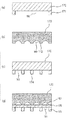
図1を参照すると、このような照明装置1は、基板20上に平坦な導光板30が配置され、この導光板30の側面には、複数の側面型LED10(一つのみ図示)がアレイ状に配置される。
【0006】
LED10から導光板30に入射された光(L)は、導光板30の下面に備えられた微細な反射パターン又は反射シート40により上部に反射されて導光板30から出射された後導光板30の上部のLCDパネル50に光を提供することになる。
【0007】
このような照明装置には、図2に示すように、上記導光板30とLCDパネル50との間に拡散シート31やプリズムシート32、33、保護シート34などの複数の光学シートをさらに付加する構造で形成することができる。
【0008】
したがって、このような導光板は、基本的に、このような照明装置の必須部品として用いられているが、これにより、導光板自体の厚さにより製品の薄型化に限界があり、大面積の照明装置の場合、画質が低下するという問題を引き起こす。
【発明の概要】
【発明が解決しようとする課題】
【0009】
本発明の実施例は、上述した問題を解決するためになされたものであり、プリント回路基板の表面に離隔領域を有する反射ユニットを備え、光の反射率と共に輝度の向上を極大化し、照明装置の厚さや光源の数の増加がなくても輝度を高めることができ、離隔領域を形成する離隔部材(スペーサ)のパターンデザインにより、光の調節及び反射効率を極大化できる照明装置を提供することができる。
【0010】
なお、本発明の実施例に係る照明装置は、一般的な照明装置の構造に必須部品である導光板を除去し、フィルムタイプのレジン層を用いて光源を誘導する構造を形成することにより、光源の数を低減することができ、照明装置の全体の厚さを薄型化し、製品のデザインの自由度を高めることができる信頼性の高い製品を提供することができる。
【課題を解決するための手段】
【0011】
上述した課題を解決するための手段として、本発明の実施例に係る照明装置は、プリント回路基板上に形成される複数のLED光源と、上記LED光源が貫通する構造で上記プリント回路基板上に積層される反射ユニットとを含み、上記反射ユニットは、上記プリント回路基板の表面に密着する金属物質を含む反射部材又は白色PET(white polyethylen terephthalte)からなる第1反射部材と、上記第1反射部材と離隔され、上記離隔領域を形成する透明材質の第2反射部材とを含む照明装置を提供する。
【0012】
これにより、プリント回路基板の表面に金属反射層を含む反射ユニットを備え、光の反射率と共に輝度の向上を極大化し、さらに上記反射ユニットを白色PETを用いて離隔領域を実現することにより、光の反射率と共に輝度の向上を極大化し、照明装置の厚さや光源の数の増加がなくても輝度を高めることができ、離隔領域を形成する離隔部材(スペーサ)のパターンデザインにより、光の調節及び反射効率を極大化することができる。
【発明の効果】
【0013】
本発明によれば、プリント回路基板の表面に離隔領域を有する反射ユニットを金属反射物質を用いるか、又は白色PETを用いて実現することにより、光の反射率と共に輝度の向上を極大化し、照明装置の厚さや光源の数の増加がなくても輝度を高めることができ、離隔領域を形成する離隔部材(スペーサ)のパターンデザインにより、光の調節や反射効率を極大化できる効果もある。
【0014】
なお、本発明は、光学パターンを備える光学パターン層を形成し、接着物質をパターニング(接着パターン層)して離隔領域を備えることにより、遮光パターン部分に発生するホットスポット及び暗部の発生を除去することができ、接着物質と接着される部品間の信頼性が確保されると共に、光学的特性の有意差がない照明装置を実現することができ、部品間の精密なアラインが可能である効果がある。
【0015】
なお、拡散板にパターニングしたり、別途の部材を用いて離隔層を備えた離隔モジュールを備えることにより、照明装置の拡散及び光の均一性の光学特性を向上させることができる効果がある。
【0016】
なお、一般的な照明装置の構造に必須部品である導光板を除去し、フィルムタイプのレジン層を用いて光源を誘導する構造を形成することにより、光源の数を低減することができ、照明装置の全体の厚さを薄型化し、製品のデザインの自由度を高めることができる効果がある。
【0017】
特に、側面型発光ダイオードを直下に実装して光源の数を大幅に低減しながらも、光学特性を確保することができ、導光板を除去してフレキシブルディスプレイの構造にも適用可能であり、レジン層に反射パターンを含む反射部材及び離隔層を含む拡散板を備えて安定した発光特性を確保できる効果もある。
【図面の簡単な説明】
【0018】
【図1】従来の照明装置の構造を示す概念図である。
【図2】従来の照明装置の構造を示す概念図である。
【図3】本発明に係る照明装置の要部を示す断面概念図である。
【図4】図3に示される本発明に係る照明装置に含まれる反射ユニットを構成する離隔部材の一例を示す図である。
【図5】本発明に係る反射ユニットの一例を示す概念図である。
【図6】本発明に係る反射ユニットの効率を比較した結果表である。
【図7】本発明に係る照明装置の他の実施例を示す図である。
【図8】本発明に係る照明装置の又他の実施例を示す図である。
【図9】本発明に係る光学パターン層に実現される様々な例を示す図である。
【図10】本発明に係る拡散板に実現される様々な例を示す図である。
【発明を実施するための形態】
【0019】
以下では、添付の図を参照して本発明に係る構成及び作用を具体的に説明する。添付の図を参照して説明するに当たり、図面符号に関係なく同一の構成要素は同一の参照符号を付与し、これについての重複説明は省略する。第1、第2等の用語は様々な構成要素を説明するのに使用できるが、上記構成要素は上記用語により限定されてはならない。上記用語は一つの構成要素を他の構成要素と区別する目的のみで使用される。
【0020】
本発明は、LEDを光源として用いる照明装置においてLED光源の下部に離隔領域を備えた反射ユニットを配置して反射率及び輝度を向上させることを要旨とする。特に、従来の照明装置の構造において接着物質をパターニング(接着パターン層)して離隔領域を形成する光学パターン層又は拡散板にパターニングしたり、別途の部材を用いて離隔層を備えた離隔モジュールを備えることにより光学特性を改善し、特に導光板を除去し、これをレジン層で形成することにより、照明装置の全体の厚さを格段に減少させる一方、光源の数を低減できる構造を提供することを要旨とする。
(第1の実施例)
図3は、本発明に係る照明装置の要部を示す断面概念図である。
【0021】
図3を参照すると、本発明に係る照明装置は、プリント回路基板110上に形成される複数のLED光源130を備え、上記プリント回路基板110の上部面には、上記LED光源130が貫通する構造で上記プリント回路基板110上に積層される反射ユニット120を含んで構成される。特に、この場合、上記反射ユニット120の内部に離隔(air)領域A1を備えることを特徴とする。上記離隔領域A1は、上記光源130から出射する光の反射効率を向上させて輝度を極大化することができる。
【0022】
特に、上記反射ユニット120は、上記プリント回路基板110の表面に密着する第1反射部材121と、上記第1反射部材121と離隔され、上記離隔領域A1を形成する透明材質の第2反射部材122とを含んで構成することができる。上記第1及び第2反射部材121、122は、上記プリント回路基板上に積層され、上記反射部材上に形成された孔を貫通してLED光源130が外部に突出することになる。
【0023】
上記離隔領域A1の形成は、上記第1及び第2反射部材121、122を別途の接着剤などの部材を用いずに、一体に圧着された構造で形成することが可能であり、さらに図示されているように、別途の接着部材などの離隔部材123により空気が収容されている離隔領域A1を形成するために、上記第1および第2反射部材121、122を離隔させて形成することも可能である。
【0024】
この場合、上記第1反射部材121は、光を反射させる反射物質、即ち、Agなどの金属層が形成されたフィルムを用いることができ、上記第2反射部材122は、上記LEDから出射された光が上記第1反射部材122の表面に伝達されて再反射されるように透明な素材のフィルムを用いることがより望ましい。特に、本発明において上記第1反射部材121は、光を反射させる反射構造物として特に白色PETを用いることが望ましい。即ち、本発明に係る特有の反射ユニットにおいて、第1反射部材は、一般的な金属反射物質層(Agなど)で形成することも可能であるが、輝度向上の極大化のためには白色PETを用いることが良い。反射ユニットの実現において、白色PETを用いて第1反射部材を形成する場合、従来に比べ約30%の輝度向上の効果を得ることができる。
【0025】
特に、上記光源130から出射された光が第1反射部材を透過して第2反射部材で再反射されること以外にも、第2反射部材122の表面に白色印刷により反射パターン124を備えることにより、光の分散をより促進させて輝度を向上させることがより望ましい。光の反射率を大幅に向上できるように反射パターン130を備え、上記反射パターンは、TiO2、CaCO3、BaSO4、Al2O3、シリコン、PSのうちいずれか一つを含む反射インクを用いて印刷することができる。
【0026】
特に、本発明に係る照明装置の光源は様々な種類の光源の適用が可能であり、特に望ましくは側面発光型構造のLEDを用いることができ、この場合、上記反射パターンはLED光源の光出射方向に形成することが望ましく、特に、上記LED光源の出射方向から遠ざかるほどパターン密度が高くなるようにパターンを配置できる。側面発光型構造のLEDを用いる場合、光源の数を大幅に低減することができるという利点がある。
【0027】
図4は、図3に示される本発明に係る照明装置に含まれる反射ユニットを構成する離隔部材の一例を示す図である。
【0028】
即ち、本発明に係る離隔部材は、第1反射部材と第2反射部材を単純に離隔させるスペーサ部材や接着性を有するスペーサ部材などの一般的な離隔機能を行って離隔領域を形成することも可能であるが、より望ましくは、離隔領域の配置を効率化すると共に接着効率を向上させるために、離隔部材を、図4に示すようなパターニング構造で均一に又はランダムにパターニングして形成することができる。
【0029】
図4に示すように、離隔部材123は、内部に空洞部が形成される単位離隔部材123aが複数配置され、上記単位離隔部材123aの内側に空いている構造で第1離隔部123bが形成される、2次元又は3次元的な構造で形成することができる。即ち、上記単位離隔部材123aの断面は多角形状、円状、楕円状など様々な形状に形成できる。特に、図示されたように、それぞれの一つの単位離隔部材123aが複数個密着して配置される構造以外にも、相互に不規則な構造で配置されて単位離隔部材123aの内部の第1離隔部123bと、それぞれの単位離隔部材123a間の空いている空間の第2離隔部123cとから形成することも可能である。
【0030】
図5は、図3及び図4に示される反射ユニットの具体的な一例を示す図である。本発明に係る反射ユニット120は、上述したように、上記プリント回路基板の表面に密着する第1反射部材121と、上記第1反射部材と対向するように離隔して配置される第2反射部材122とを含む。特に、上記第2反射部材122は、PETなどの透明な材質のフィルムを適用でき、接着物質をパターニングして上記第1および第2反射部材121、122を離隔させる離隔部材123を備えて離隔領域を形成する。
【0031】
特に、反射効率の極大化のために上記第1反射部材121は、金属反射層125を接着剤(primer; T1、T2)を媒介として接着する光学フィルム126を備え、上記光学フィルム126もリリースフィルム128上に接着物質(PSA)127を媒介として積層される構造で形成することができる。
【0032】
図5に示す構造において、第1反射部材の実施例とは異なり、上記第1反射部材121は、光を反射させる反射構造物として白色PETを用いて形成することができる。
【0033】
図6は、本発明に係る反射ユニットの構造を実現する場合における照明装置の輝度向上の程度を比較するための結果表である(CIE X、CIE Yは色度表である。)。
図示された表は、(A)は図3に示す構造においてプリント回路基板の表面にAgから形成される反射部材1枚のみを形成した場合の輝度を測定したものであり、(B)は本発明に係る反射ユニットの構造、即ち接着パターン物質をシリコンから形成して図4のパターンを形成し、第1反射部材をAgフィルムとした場合における、従来の(A)構造と比較して輝度向上の結果値を測定したものである。
【0034】
又、(C)は(B)とは異なり、第1反射部材を白色PETから形成し、これにより、従来の(A)構造と比較して輝度向上の結果値を測定したものである。
【0035】
測定結果、(A)の場合、輝度が6605nitであり、これを基準にする場合、(B)の構造では輝度が7468nitであって、約13%の輝度向上の結果を示し、本発明に係る白色PETを含んで形成した反射ユニットの場合である(C)では輝度が8472nitであって、(A)に比べ28.6%の輝度上昇率を示している。即ち、接着物質層をパターニングした構造(離隔領域)を備えると共に、白色PETを用いる場合、輝度向上の極大化を実現することができる。
【0036】
(第2の実施例)
図7は、本発明に係る照明装置の他の実施例を示すものである。
【0037】
即ち、本発明に係る第2の実施例は、上述した第1の実施例での上記プリント回路基板上に光ガイド部材を積層する構造を実現するものである。上記光ガイド部材としてはレジン層を用いることができ、このようなレジン層は、液晶表示装置の照明装置などで使用されるプレート状の導光板を代替する構成に該当するものであり、光源から出射する光を前方に誘導する機能を実行することになる。
【0038】
図7を参照すると、本発明に係る照明装置は、プリント回路基板110上に形成される複数のLED光源130と出射される光を前方に拡散及び誘導する光ガイド部材をさらに含んで構成される。以下、上記光ガイド部材をレジン層で実現する実施例について説明する。
即ち、上記レジン層140は、上記LED光源130の周りを取り囲む構造で積層され、側方向に出射する光源の光を分散させる機能を実行することになる。即ち、従来の導光板の機能を上記レジン層140で行うようになる。
【0039】
上記レジン層は、基本的に光を拡散させることができる材質の樹脂であれば特に制限がない。一例として、本発明に係る一実施例としてのレジン層はウレタンアクリレートオリゴマーを主原料とするレジンを用いることができる。例えば、合成オリゴマーであるウレタンアクリレートオリゴマーをポリアクリルであるポリマータイプと混合したものを用いることができる。もちろん、ここに低沸点希釈型反応性モノマーであるIBOA(isobornyl acrylate)、HPA(Hydroxylpropyl acrylate)、2-HEA(2-Hydroxyethyl acrylate)などが混合されたモノマーをさらに含むことができ、添加剤として光開始剤(例えば、1-ヒドロキシシクロヘキシルフェニルケトン(1-hydroxycyclohexyl phenyl-ketone)など)又は酸化防止剤などを混合することができる。
【0040】
なお、上記レジン層140は、光の拡散と反射を増加させるために光拡散体141を含むことができる。この場合、上記光拡散体はビーズ(bead)を含むことができる。上記ビーズはレジン層の全体重量に対して0.01〜0.3%含むことが望ましい。即ち、LEDから側方向に出射される光は、上記レジン層140とビーズにより拡散及び反射されて上部方向に進行するようになる。
【0041】
これは上述した本発明に係る反射ユニット120と共に反射機能をより促進させることができる。したがって、上記レジン層の存在は、従来の導光板が占めていた厚さを格段に減少させ、製品の薄型化を実現できることは勿論、軟性の性質を有するようになり、フレキシブルなディスプレイにも適用できる汎用性を備えるようになる。
【0042】
(第3の実施例)
上述した第2の実施例の構造から改良された構造で上記レジン層上に光の拡散を促進させる光学パターン層が形成される第3の実施例の照明装置の構造を説明する。
【0043】
即ち、図8を参照すると、本発明に係る照明装置は、図7に示される上記レジン層140の上部に配置され、光学パターン151を含む光学パターン層150を備える構造で形成することができる。
【0044】
特に、上記光学パターン層150は、上記光学パターンの周辺部を取り囲む第2離隔領域152を形成する接着パターン層153を含んで構成することができる。即ち、上記接着パターン層153は、上記光学パターン151に一定の形状のパターンを有する離隔された空間(第2離隔領域)を形成し、その他の部分には接着物質を塗布して形成する。
【0045】
即ち、図示された構造において上記光学パターン層150と接着パターン層153の配置関係で、上記光学パターン層150は、上記光学パターンを内部に含む第1基板150A及び第2基板150Bを備え、上記接着パターン層153は、上記遮光パターンの周辺部を取り囲む上記第2離隔領域152以外の部分に塗布され、第1基板150A及び第2基板150Bを接着させる。
【0046】
即ち、上記光学パターン151は、上記LED光源130から出射する光の集中を防ぐために遮光パターンで形成でき、このためには、上記光学パターン151とLED光源130との間にアライン(align)が必要であり、アライン後固定力を確保するために接着部材(adhensive)を用いて接着することになる。
【0047】
上記第1基板150A及び第2基板150Bは、光透過率に優れた材質の基板を用いることができ、一例としてPETを用いることができる。この場合、上記第1基板150A及び第2基板150Bの間に配置される光学パターン151は、基本的にLED光源から出射される光が集中しないようにする機能をし、上記第1基板150A又は第2基板150Bのいずれかに遮光印刷により形成でき、上記遮光パターンの周辺部を取り囲む構造で接着物質を塗布した接着層を介して二基板を接着してアラインを実現する。即ち、上記第1基板150A及び第2基板150Bの接着構造は、印刷された遮光パターン151を固定する機能をさらに実行することになる。又、上記接着層は、熱硬化型PSA、熱硬化型接着剤、UV硬化型PSAタイプの物質を用いることができる。
【0048】
上記接着パターン層153を形成して接着する時、第2離隔領域152を形成するパターン構造で接着すると、接着物質が遮光パターンに重なって発生する強いホットスポット(Hot spot)又は暗部の発生を防ぐことができ、離隔層(air layer)の存在により光の均一性を高めることができるようになる。
【0049】
上述した構造の本発明に係る照明装置は、上述した構成に加えて、上記レジン層140の上部に拡散板170を備えることができ、上記拡散板170と上記光学パターン層150との間に第3離隔領域161を備えた離隔モジュール160をさらに備えることができる。なお、上記拡散板の上部にプリズムシート、保護シートなどが付加的に備えられる。
【0050】
図9は、上記光学パターン151と接着パターン層153、そしてこれにより形成される第2離隔領域152の構成を概念的に示す図である。
【0051】
上記第1基板上に特定のパターンで印刷される光学パターン151の周辺部を取り囲む構造で接着物質を用いて接着パターン層153を形成すると、一定の離隔空間が形成されながら第2基板150Bが接着される。このような離隔空間は離隔層が形成された密閉構造となり、これを‘第2離隔領域’と定義する。上記接着パターン層153が形成する上記第1離隔領域152の平面形状は、円形、楕円形、長方形、正方形、多角形など様々な形状に形成できる。又、上記接着パターン層は熱硬化型PSA、熱硬化型接着剤、UV硬化型PSAタイプの物質を用いて形成できる。
【0052】
又、上記光学パターン151は、光の強度が過度に強くて光学特性が悪くなったり、黄色光が導き出される(yellowish)現象を防止するために一定部分の遮光効果が出るように遮光パターンで形成されることが望ましい。即ち、光が集中しないように遮光インクを用いて遮光パターンを印刷できる。
【0053】
上記光学パターンは、光を完全に遮断する機能ではなく、光の一部遮光および拡散機能を実行できるように一つの光学パターンで光の遮光度や拡散度を調節できるように形成することができる。より望ましくは、本発明に係る光学パターンは、複合的なパターンの重畳印刷構造で形成することもできる。重畳印刷構造とは一つのパターンを形成し、その上部にもう一つのパターン形状を印刷して形成する構造をいう。
【0054】
一例としては、上記光学パターン151は、光の出射方向に高分子フィルムの下面にTiO2、CaCO3、BaSo4、Al2O3、シリコンから選択されるいずれか一つ以上の物質を含む遮光インクを用いて形成される拡散パターンと、Al又はAlとTiO2の混合物質を含む遮光インクを用いた遮光パターンの重畳印刷構造で形成することができる。 即ち、高分子フィルムの表面に拡散パターンを白色印刷して形成した後、その上に遮光パターンを形成したり、これとは逆の順序で2重構造で形成することも可能である。勿論、このようなパターン形成のデザインは光の効率と強度、遮光率を考慮して多様に変形できることは自明であろう。又は、順次積層構造において中央層に金属パターンの遮光パターンを形成し、その上部と下部にそれぞれ拡散パターンを形成する3重構造で形成することも可能である。このような3重構造においては上述した物質を選択して形成することが可能であり、望ましい一例としては、屈折率に優れたTiO2を用いて拡散パターンのいずれか一つを形成し、光安定性と色感に優れたCaCO3をTiO2と共に用いて他の拡散パターンを形成し、隠蔽性に優れたAlを用いて遮光パターンを形成する3重構造により光の効率性と均一性を確保することができる。特にCaCO3は黄色光の露出を遮断する機能により、最終的に白色光を実現するように機能をすることでより安定した光の効率を実現でき、CaCO3以外にもBaSO4、Al2O3、シリコンビーズなどの粒子サイズが大きく、類似の構造を有する無機材料を活用することもできる。さらに、光学パターンは、上記LED光源の出射方向から遠ざかるほどパターン密度が低くなるようにパターン密度を調節して形成することが光効率の面で望ましい。
【0055】
なお、本発明は、光学パターン層150と拡散板170との間に配置される離隔モジュールをさらに含んで形成できる。
【0056】
図10は、図8に示す光学パターン層150と拡散板170との間に配置される離隔モジュールを形成する一例を示す図である。
【0057】
即ち、本発明に係る照明装置の構成には、光学パターン層150と拡散板170との間に離隔層(第3離隔領域)160を備える構造をさらに含ませることができ、上記第3領域161の存在により、上記光源から出射された光を拡散させ、光の均一性(uniformity)を向上させることができる効果が実現される。なお、上記レジン層140と光学パターン層150を透過した光のばらつきを最小化するために、上記第3離隔領域160の厚さは0.01〜2mmの範囲で形成することが望ましい。
【0058】
上記第3離隔領域160は、拡散板の下部に離隔層を形成できる構造で形成することができ、このような構造により形成される第3離隔領域を含んで‘離隔モジュール’と定義する。
【0059】
上記離隔モジュールは、拡散板自体を加工してむ離隔領域(離隔層)を形成したり、又は拡散板の下部に別途の構造物を形成して離隔領域を形成する構成などを全て含む。
【0060】
即ち、図10の(a)に示すように、拡散板170の下部にスペーサ171を形成して第3離隔領域160を形成したり、(b)に示すように、拡散板の下部をパターニングして下部の層と密着して第3離隔領域(air area)160を形成するブリッジ172の構造で形成することができる。
【0061】
このような一体型構造は、上記パターニングされた形状、すなわち、離隔領域を形成するパターンの形状に応じて多様に変形させることができ、これによりブリッジの形状も多様に変形させることできることは自明であり、これも本発明の要旨に含まれる。さらに(c)に示す構造のように、拡散板の下面自体をパターニングする方法以外に、別途の構造物を用いて離隔領域160を形成する構造でも形成することができる。もちろん、図示された構造物は、スペーサ部材としてブリッジ174を備える構造を例示したが、本発明の要旨はこのような方法を含み、拡散板の下部に離隔層を形成できる様々な変形例も本発明の要旨に該当することは言うまでもない。
【0062】
(d)に示すように、拡散板自体をパターニングする(b)の構成や、別途の構造物を用いる(c)の構成のように、離隔層を単一層にすること以外にも、独立した離隔層を形成できる構造175、176を採用して複数の層で離隔領域160、161を形成することも可能である。
【0063】
なお、本発明に係る照明装置は、照明を必要とする様々なランプ装置、例えば車両用ランプ、家庭用照明装置、産業用照明装置への適用が可能であることはもちろんである。車両用ランプは、ヘッドライト、室内照明、テールライトなどにも適用が可能である。上述した本発明に係る照明装置が次のような構成と作用によりLCDに適用される一例を挙げて説明すると次の通りである。
本発明に係る照明装置は、光源の数を減らすために、上記LED光源130は側面発光LEDを採用して配置できる。図8を参照すると側面発光型LED130から側方向に光が出射され、出射された光は従来の導光板の代わりに形成されたレジン層140で反射及び拡散され、光学パターン層150により光の集中を防ぎ、拡散板の下部に形成された第3離隔領域により光のばらつきを最小化できる。特に、上記レジン層140とプリント回路基板110との間に配置される本発明に係る反射ユニット120の存在により、反射率をより向上させることができ、光の効率性を極大化し輝度向上の効果を実現することができる。特に、本発明に係る反射ユニット120の場合、接着物質層のパターニングにより離隔領域を形成するデザインを多様に変形して反射率を調節でき、パターニングされた接着物質の材料及び種類に応じて反射率、色の実現を調整できる効果もある。さらに、第2反射部材122の光の特性及び厚さに応じて反射率を調節することもできる。
【0064】
まとめると、本発明に係る反射ユニット120と反射パターン124によって出射された光はより一層反射効率が高くなり、光を前方に誘導できるようになる。このように、レジン層140を通過した光は光学パターン層150に形成された光学パターン151を通じて拡散又は遮光される過程を経て、このように精製された光は、拡散板の下部に形成される離隔モジュールにより再度光学特性が精製されて均一性を高めることができ、その後付加されるプリズムシート180、DBEF190などの光学シートを経て白色光としてLCDパネルに入射することになる。
【0065】
以上の例は、本照明装置をLCDに適用する例を挙げて説明したが、上述のように、室内用照明や車両用ランプ装置等に様々に変形して適用することができる。
【0066】
このように、本発明に係る照明装置の場合、反射ユニットの離隔領域を備えた構造により反射効率を極大化することはもちろん、導光板の構造を除去し、光の供給源として側面発光型LEDを採用し、レジン層により光を拡散及び反射させて光を誘導することで、薄型化及び光源の数を低減することができる。一方、光源の減少による輝度の低下及び均一性の問題を反射パターンと遮光パターン及び離隔モジュールの離隔領域を備えて調節できるようにして光学特性を向上させることができる。
【0067】
上述のような本発明の詳細な説明では具体的な実施例について説明した。しかし、本発明のカテゴリから逸脱しない限度内で様々な変形が可能である。本発明の技術的思想は本発明の実施例に限られてはならず、特許請求の範囲だけでなく本特許請求の範囲と均等なものにより定められなければならない。
【産業上の利用可能性】
【0068】
本発明に係る照明装置は、照明を必要とする様々なランプ装置、例えば車両用ランプ、家庭用照明装置、産業用照明装置に適用可能である。車両用ランプは、ヘッドライト、室内照明、テールライトなどにも適用可能であることは勿論である。
[Document Name] Description
[Title of the Invention]
Lighting device
[0001]
【Technical field】
[0002]
The present inventionExamples ofRelates to a lighting device using an LED as a light source, and more particularly to a structure of a lighting device that can be applied to a room lamp, a vehicle lamp, a backlight unit, and a liquid crystal display device as a thin-type lighting.
[Background]
[0003]
Devices for realizing illumination by guiding light emitted from a light source are variously required for illumination lamps, vehicle lamps, liquid crystal display devices, and the like. In such an illuminating device, a technique for reducing the structure of the equipment and a structure capable of improving the light efficiency are recognized as the most important techniques.
[0004]
A liquid crystal display device will be described as an example to which such an illumination device is applied.
[0005]
Referring to FIG. 1, in such an illumination device 1, a flat
[0006]
The light (L) incident on the
[0007]
In such an illuminating device, as shown in FIG. 2, a plurality of optical sheets such as a
[0008]
Therefore, such a light guide plate is basically used as an indispensable part of such an illuminating device. However, due to the thickness of the light guide plate itself, there is a limit to reducing the thickness of the product. In the case of an illuminating device, it causes a problem that the image quality deteriorates.
SUMMARY OF THE INVENTION
[Problems to be solved by the invention]
[0009]
The present inventionExamples ofWas made to solve the above-mentioned problems,TheOn the surface of the lint circuit boardSeparationIt has a reflection unit with a region, maximizes the improvement in luminance as well as the reflectance of light, and can increase the luminance without increasing the thickness of the lighting device and the number of light sources,SeparationTo provide a lighting device capable of maximizing light adjustment and reflection efficiency by pattern design of a separation member (spacer) that forms a regionCan.
[0010]
In addition,BookInventionAccording to the exampleLighting deviceIsThe number of light sources can be reduced by removing the light guide plate, which is an essential part of the structure of a general lighting device, and forming a structure that guides the light source using a film-type resin layer. To provide a highly reliable product that can reduce the overall thickness of the product and increase the degree of freedom in product designCan.
[Means for Solving the Problems]
[0011]
As means for solving the above-described problems, the present inventionLighting device according to the embodimentIncludes a plurality of LED light sources formed on the printed circuit board, and a reflection unit stacked on the printed circuit board in a structure through which the LED light source passes, and the reflection unit is a surface of the printed circuit board. Reflection containing metallic materials that adhere to the surfaceElementAlternatively, the first reflection made of white PET (white polyethyl terephthalate)ElementAnd the first reflectionElementSeparated from the aboveSeparationSecond reflection of transparent material forming the areaElementA lighting device is provided.
[0012]
Accordingly, a reflection unit including a metal reflection layer is provided on the surface of the printed circuit board, and the improvement in luminance is maximized together with the reflectance of light. Further, the reflection unit is made of white PET.SeparationBy realizing the area, the luminance improvement can be maximized together with the reflectance of light, and the luminance can be increased without increasing the thickness of the lighting device or the number of light sources,SeparationLight adjustment and reflection efficiency can be maximized by the pattern design of the separation member (spacer) that forms the region.
【Effect of the invention】
[0013]
According to the present invention, the surface of the printed circuit boardSeparationBy implementing a reflective unit having a region using a metal reflective material or using white PET, the luminance improvement as well as the reflectance of light is maximized, and there is no increase in the thickness of the lighting device or the number of light sources Can increase brightness,SeparationBy the pattern design of the separation member (spacer) that forms the region, there is an effect that light adjustment and reflection efficiency can be maximized.
[0014]
In the present invention, an optical pattern layer having an optical pattern is formed, and an adhesive substance is patterned (adhesive pattern layer).SeparationBy providing a region, it is possible to eliminate the occurrence of hot spots and dark portions generated in the light shielding pattern portion, ensuring reliability between the adhesive substance and the parts to be bonded, and there is no significant difference in optical characteristics. An illumination device can be realized, and there is an effect that precise alignment between components is possible.
[0015]
In addition, patterning on the diffusion plate or using a separate memberSeparationWith layerSeparationBy providing the module, there is an effect that the optical characteristics of the diffusion of the lighting device and the uniformity of light can be improved.
[0016]
The number of light sources can be reduced by removing the light guide plate, which is an essential part of the structure of a general lighting device, and forming a structure that guides the light sources using a film-type resin layer. This has the effect of reducing the overall thickness of the device and increasing the degree of freedom in product design.
[0017]
In particular, it is possible to secure the optical characteristics while mounting the side-type light-emitting diode directly under the light source, greatly reducing the number of light sources, and it can be applied to the structure of flexible displays by removing the light guide plate. Reflection including reflective pattern in layerElementas well asSeparationThere is also an effect that a stable luminescent property can be secured by providing a diffusion plate including a layer.
[Brief description of the drawings]
[0018]
FIG. 1 is a conceptual diagram showing a structure of a conventional lighting device.
FIG. 2 is a conceptual diagram showing a structure of a conventional lighting device.
FIG. 3 is a conceptual cross-sectional view showing the main part of the illumination device according to the present invention.
4 is a view showing an example of a separation member constituting a reflection unit included in the lighting apparatus according to the present invention shown in FIG.
FIG. 5 is a conceptual diagram showing an example of a reflection unit according to the present invention.
FIG. 6 is a result table comparing the efficiency of the reflecting unit according to the present invention.
FIG. 7 is a diagram showing another embodiment of the illumination device according to the present invention.
FIG. 8 is a diagram showing another embodiment of the illumination device according to the present invention.
FIG. 9 is a diagram showing various examples realized in the optical pattern layer according to the present invention.
FIG. 10 is a diagram showing various examples realized in the diffusion plate according to the present invention.
BEST MODE FOR CARRYING OUT THE INVENTION
[0019]
Hereinafter, the configuration and operation according to the present invention will be described in detail with reference to the accompanying drawings. In the description with reference to the accompanying drawings, the same constituent elements are given the same reference numerals regardless of the reference numerals, and redundant description thereof will be omitted. The terms first, second, etc. can be used to describe various components, but the components should not be limited by the terms. The above terms are used only for the purpose of distinguishing one component from other components.
[0020]
The present invention provides a lighting device that uses an LED as a light source.SeparationThe gist of the invention is to improve the reflectance and luminance by arranging a reflection unit having a region. In particular, by patterning the adhesive substance (adhesive pattern layer) in the structure of the conventional lighting deviceSeparationPatterning on the optical pattern layer or diffusion plate that forms the region, or using a separate memberSeparationWith layerSeparationBy providing a module, the optical characteristics are improved, especially by removing the light guide plate and forming it with a resin layer, thereby reducing the overall thickness of the lighting device, while reducing the number of light sources. The main point is to provide.
(First embodiment)
FIG. 3 is a conceptual cross-sectional view showing the main part of the illumination device according to the present invention.
[0021]
Referring to FIG. 3, the lighting device according to the present invention includes a plurality of LED
[0022]
In particular, the
[0023]
the aboveSeparationThe region A1 is formed by the first and second reflections.Element121 and 122 can be formed with a structure in which they are integrally pressure-bonded without using a separate member such as an adhesive. Further, as shown in the drawing, the
[0024]
In this case, the first reflectionElement121 may be a reflective material that reflects light, that is, a film on which a metal layer such as Ag is formed.
[0025]
In particular, the light emitted from the
[0026]
In particular, the light source of the lighting device according to the present invention can be applied to various types of light sources, and particularly preferably, a side-emitting LED can be used. In this case, the reflection pattern is a light emission of the LED light source. Preferably, the pattern can be arranged so that the pattern density increases as the distance from the emission direction of the LED light source increases. In the case of using an LED having a side-emitting structure, there is an advantage that the number of light sources can be greatly reduced.
[0027]
FIG. 4 is a view showing an example of a separation member constituting the reflection unit included in the lighting apparatus according to the present invention shown in FIG.
[0028]
In other words, the separation member according to the present invention has the first reflection.ElementAnd second reflectionElementPerform general separation functions such as spacer members that simply separate the spacers and spacer members that have adhesive propertiesSeparationIt is possible to form a region, but more desirably,SeparationIn order to improve the arrangement of the regions and improve the adhesion efficiency, the separation member can be formed by patterning uniformly or randomly with a patterning structure as shown in FIG.
[0029]
As shown in FIG. 4, the
[0030]
FIG. 5 is a diagram showing a specific example of the reflection unit shown in FIGS. 3 and 4. As described above, the
[0031]
In particular, the first reflection is used to maximize the reflection efficiency.Element121 includes an
[0032]
In the structure shown in FIG.ElementUnlike the first embodiment, the first reflectionElement121 can be formed using white PET as a reflective structure for reflecting light.
[0033]
FIG. 6 is a result table for comparing the degree of improvement in luminance of the illumination device when the structure of the reflection unit according to the present invention is realized (CIE X and CIE Y are chromaticity tables).
The table shown shows that (A) is a reflection formed from Ag on the surface of the printed circuit board in the structure shown in FIG.ElementThe brightness when only one sheet is formed is measured. (B) shows the structure of the reflection unit according to the present invention, that is, the adhesive pattern material is formed of silicon to form the pattern of FIG.ElementIs a result of measuring the luminance improvement in comparison with the conventional structure (A) in the case of using an Ag film.
[0034]
Also, (C) is different from (B) and the first reflectionElementIs formed from white PET, and as a result, the result of brightness improvement is measured as compared with the conventional structure (A).
[0035]
As a result of the measurement, in the case of (A), the luminance is 6605 nits, and when this is used as a reference, the luminance of the structure of (B) is 7468 nits and shows a result of about 13% luminance improvement. In (C), which is a case of a reflection unit formed by including white PET, the luminance is 8472 nit, which is 28.6% higher than that in (A). That is, a structure in which the adhesive material layer is patterned (SeparationArea) and using white PET, it is possible to maximize the luminance.
[0036]
(Second embodiment)
FIG. 7 shows another embodiment of the lighting device according to the present invention.
[0037]
That is, the second embodiment according to the present invention is formed on the printed circuit board in the first embodiment described above.Light guide memberThe structure which laminates | stacks is realized. the aboveAs a light guide memberResin layerCan be used,like thisThe resin layer corresponds to a configuration that substitutes for a plate-shaped light guide plate used in a lighting device of a liquid crystal display device, and performs a function of guiding light emitted from a light source forward.
[0038]
FigureReferring to FIG. 7, the lighting device according to the present invention diffuses and guides a plurality of LED
That is, the
[0039]
The resin layer is not particularly limited as long as it is basically a resin that can diffuse light. As an example, the resin layer as one embodiment according to the present invention can use a resin mainly composed of urethane acrylate oligomer. For example, a urethane acrylate oligomer that is a synthetic oligomer mixed with a polymer type that is polyacryl can be used. Of course, it may further contain a monomer mixed with IBOA (isopropyl acrylate), HPA (Hydroxypropyl acrylate), 2-HEA (2-Hydroxyethyl acrylate), etc., which are low-boiling dilution reactive monomers. A photoinitiator (for example, 1-hydroxycyclohexyl phenyl-ketone) or an antioxidant can be mixed.
[0040]
The
[0041]
This can further promote the reflection function together with the
[0042]
(Third embodiment)
The structure of the illumination apparatus of the third embodiment, in which an optical pattern layer that promotes the diffusion of light on the resin layer, is improved from the structure of the second embodiment described above.
[0043]
That is, referring to FIG. 8, the illumination device according to the present invention may be formed with a structure including an
[0044]
In particular, the
[0045]
That is, in the illustrated structure, the
[0046]
That is, the
[0047]
As the
[0048]
When the
[0049]
In addition to the above-described configuration, the lighting device according to the present invention having the above-described structure may include a
[0050]
FIG. 9 shows the
[0051]
When the
[0052]
In addition, the
[0053]
The optical pattern is not a function of completely blocking light, but can be formed so that the degree of light blocking and diffusing of light can be adjusted with one optical pattern so that a part of the light can be blocked and diffused. . More preferably, the optical pattern according to the present invention can be formed by a composite pattern overlapping printing structure. The superimposed printing structure is a structure in which one pattern is formed and another pattern shape is printed thereon.
[0054]
As an example, the
[0055]
In the present invention, the
[0056]
10 is disposed between the
[0057]
That is, in the configuration of the illumination device according to the present invention, between the
[0058]
[0059]
the aboveSeparationThe module only needs to process the diffuser plate itself.Separationregion(SeparationLayer) or a separate structure at the bottom of the diffuserSeparationAll configurations for forming a region are included.
[0060]
That is, as shown in FIG. 10A, a
[0061]
Such a monolithic structure has the patterned shape, i.e.SeparationIt is obvious that various changes can be made in accordance with the shape of the pattern forming the region, and thus the shape of the bridge can be changed in various ways. This is also included in the gist of the present invention. In addition to the method of patterning the lower surface of the diffusion plate itself as in the structure shown in (c), a separate structure is used.SeparationA structure in which the
[0062]
As shown in (d), like the configuration of (b) for patterning the diffusion plate itself or the configuration of (c) using a separate structure,SeparationIn addition to making the layer a single layer,
[0063]
The lighting device according to the present invention can be applied to various lamp devices that require lighting, such as a vehicle lamp, a home lighting device, and an industrial lighting device. The vehicle lamp can also be applied to headlights, indoor lighting, taillights, and the like. An example in which the above-described illumination device according to the present invention is applied to an LCD with the following configuration and operation will be described.
BookIn the illuminating device according to the invention, the LED
[0064]
In summary, the light emitted by the
[0065]
The above example has been described with reference to an example in which the present lighting device is applied to an LCD. However, as described above, the lighting device can be variously modified and applied to indoor lighting, a vehicle lamp device, and the like.
[0066]
Thus, in the case of the illumination device according to the present invention, the reflection unitSeparationNot only can the reflection efficiency be maximized by the structure with the area, but also the structure of the light guide plate is removed, the side-emitting LED is adopted as the light supply source, and the light is diffused and reflected by the resin layer to guide the light. By doing so, thickness reduction and the number of light sources can be reduced. On the other hand, the reduction in brightness and uniformity due to the decrease in the light sourceSeparationModuleSeparationThe optical characteristics can be improved by adjusting the area.
[0067]
In the foregoing detailed description of the invention, specific embodiments have been described. However, various modifications are possible without departing from the category of the present invention. The technical idea of the present invention should not be limited to the embodiments of the present invention, but should be defined not only by the claims but also by the equivalents of the claims.
[Industrial applicability]
[0068]
The lighting device according to the present invention can be applied to various lamp devices that require lighting, such as vehicle lamps, home lighting devices, and industrial lighting devices. Of course, the vehicle lamp can be applied to a headlight, indoor lighting, taillight, and the like.
Claims (22)
上記プリント回路基板上の反射ユニットと、
上記反射ユニットの内部に形成される離隔(air)領域と、を含む照明装置であって、
上記反射ユニットは、
上記プリント回路基板の表面の第1反射部材と、
上記第1反射部材と離隔され、上記離隔領域を形成する第2反射部材と、を含み、
上記光源は、上記反射ユニットを貫通し、
上記照明装置は、
上記反射ユニットの上面に上記光源を埋める光ガイド部材をさらに含む照明装置。 Multiple light sources on a printed circuit board;
A reflective unit on the printed circuit board;
An illuminating device including an air region formed inside the reflection unit,
The reflection unit is
A first reflecting member on the surface of the printed circuit board;
A second reflective member that is spaced apart from the first reflective member and forms the separated region,
The light source penetrates the reflection unit,
The lighting device is
The illumination device further includes a light guide member that fills the light source on an upper surface of the reflection unit.
上記光学パターンは、複合的なパターンの重畳印刷構造である請求項1乃至3のいずれか一項に記載の照明装置。 The illumination device includes an optical pattern layer including an optical pattern on the light guide member,
The illumination device according to any one of claims 1 to 3, wherein the optical pattern has a composite pattern overlapping printing structure.
上記光学パターンは、遮光パターンを含む請求項1乃至3のいずれか一項に記載の照明装置。 The illumination device includes an optical pattern layer including an optical pattern on the light guide member,
The optical pattern is illumination device according to any one of claims 1 to 3 comprising a light-shielding pattern.
上記光学パターン層は、上記光学パターンの周辺部を取り囲む第2離隔領域を形成する接着パターン層を含んで構成される請求項1乃至3のいずれか一項に記載の照明装置。 The illumination device includes an optical pattern layer including an optical pattern on the light guide member,
The optical pattern layer, the lighting apparatus according to any one of constituted claims 1 to 3 comprising an adhesive pattern layer to form a second separation region surrounding the periphery of the optical pattern.
上記光学パターン層は、上記光学パターンを内部に含む第1基板及び第2基板の間に形成される請求項1乃至3のいずれか一項に記載の照明装置。 The illumination device includes an optical pattern layer including an optical pattern on the light guide member,
The optical pattern layer, the lighting device according to any one of claims 1 to 3 is formed between the first substrate and the second substrate including the optical pattern therein.
上記光学パターンは、CaCO 3 、BaSO 4 、Al 2 O 3 、シリコン元素から選択されるいずれか一つ以上の物質を含む請求項1乃至3のいずれか一項に記載の照明装置。 The illumination device includes an optical pattern layer including an optical pattern on the light guide member,
The lighting device according to any one of claims 1 to 3 , wherein the optical pattern includes one or more substances selected from CaCO 3 , BaSO 4 , Al 2 O 3 , and silicon element .
上記プリント回路基板上の反射ユニットと、
上記反射ユニットの内部に形成される離隔(air)領域と、を含む照明装置であって、
上記照明装置は、上記反射ユニットの上面に上記光源を埋める光ガイド部材をさらに含み、
上記照明装置は、上記光ガイド部材の上部に光学パターンを含む光学パターン層を含み、
上記光学パターン層は、
上記光学パターンの周辺部を取り囲む第2離隔領域を形成する接着パターン層を含んで構成される照明装置。 Multiple light sources on a printed circuit board;
A reflective unit on the printed circuit board;
An illuminating device including an air region formed inside the reflection unit,
The illumination device further includes a light guide member that fills the light source on an upper surface of the reflection unit,
The illumination device includes an optical pattern layer including an optical pattern on the light guide member,
The optical pattern layer is
An illuminating device comprising an adhesive pattern layer forming a second separation region surrounding a peripheral portion of the optical pattern.
上記プリント回路基板上の反射ユニットと、
上記反射ユニットの内部に形成される離隔(air)領域と、を含む照明装置であって、
上記照明装置は、上記反射ユニットの上面に上記光源を埋める光ガイド部材をさらに含み、
上記照明装置は、上記光ガイド部材の上部に光学パターンを含む光学パターン層を含み、
上記光学パターン層は、
上記光学パターンを内部に含む第1基板及び第2基板の間に形成される照明装置。 Multiple light sources on a printed circuit board;
A reflective unit on the printed circuit board;
An illuminating device including an air region formed inside the reflection unit,
The illumination device further includes a light guide member that fills the light source on an upper surface of the reflection unit,
The illumination device includes an optical pattern layer including an optical pattern on the light guide member,
The optical pattern layer is
An illumination device formed between a first substrate and a second substrate including the optical pattern therein.
CaCO 3 、BaSO 4 、Al 2 O 3 、シリコン元素から選択されるいずれか一つ以上の物質を含んで形成される請求項9乃至12のいずれか一項に記載の照明装置。 Above Symbol optical pattern,
The lighting device according to any one of claims 9 to 12, wherein the lighting device is formed to include one or more substances selected from CaCO 3 , BaSO 4 , Al 2 O 3 , and silicon elements .
Applications Claiming Priority (9)
| Application Number | Priority Date | Filing Date | Title |
|---|---|---|---|
| KR20110030697 | 2011-04-04 | ||
| KR10-2011-0030697 | 2011-04-04 | ||
| KR10-2011-0070270 | 2011-07-15 | ||
| KR20110070270 | 2011-07-15 | ||
| KR1020120017282A KR101399048B1 (en) | 2011-07-15 | 2012-02-21 | Lamp device within resin layer for light-guide and LCD using the same |
| KR10-2012-0017280 | 2012-02-21 | ||
| KR10-2012-0017282 | 2012-02-21 | ||
| KR1020120017280A KR101399039B1 (en) | 2011-04-04 | 2012-02-21 | Light umit within resin layer for light-guide and LCD using the same |
| PCT/KR2012/002532 WO2012138123A2 (en) | 2011-04-04 | 2012-04-04 | Lighting apparatus |
Related Child Applications (1)
| Application Number | Title | Priority Date | Filing Date |
|---|---|---|---|
| JP2017202450A Division JP6404432B2 (en) | 2011-04-04 | 2017-10-19 | Lighting device |
Publications (2)
| Publication Number | Publication Date |
|---|---|
| JP2014510387A JP2014510387A (en) | 2014-04-24 |
| JP6231473B2 true JP6231473B2 (en) | 2017-11-15 |
Family
ID=48138689
Family Applications (7)
| Application Number | Title | Priority Date | Filing Date |
|---|---|---|---|
| JP2014503594A Active JP6231473B2 (en) | 2011-04-04 | 2012-04-04 | Lighting device |
| JP2017202450A Active JP6404432B2 (en) | 2011-04-04 | 2017-10-19 | Lighting device |
| JP2018170670A Active JP6704967B2 (en) | 2011-04-04 | 2018-09-12 | Lighting equipment |
| JP2020084405A Active JP6961751B2 (en) | 2011-04-04 | 2020-05-13 | Lighting device |
| JP2021168973A Active JP7179139B2 (en) | 2011-04-04 | 2021-10-14 | lighting equipment |
| JP2022182722A Active JP7383780B2 (en) | 2011-04-04 | 2022-11-15 | lighting equipment |
| JP2023191111A Pending JP2024014919A (en) | 2011-04-04 | 2023-11-08 | lighting equipment |
Family Applications After (6)
| Application Number | Title | Priority Date | Filing Date |
|---|---|---|---|
| JP2017202450A Active JP6404432B2 (en) | 2011-04-04 | 2017-10-19 | Lighting device |
| JP2018170670A Active JP6704967B2 (en) | 2011-04-04 | 2018-09-12 | Lighting equipment |
| JP2020084405A Active JP6961751B2 (en) | 2011-04-04 | 2020-05-13 | Lighting device |
| JP2021168973A Active JP7179139B2 (en) | 2011-04-04 | 2021-10-14 | lighting equipment |
| JP2022182722A Active JP7383780B2 (en) | 2011-04-04 | 2022-11-15 | lighting equipment |
| JP2023191111A Pending JP2024014919A (en) | 2011-04-04 | 2023-11-08 | lighting equipment |
Country Status (6)
| Country | Link |
|---|---|
| US (8) | US9279546B2 (en) |
| EP (3) | EP3591462B1 (en) |
| JP (7) | JP6231473B2 (en) |
| CN (4) | CN103597270B (en) |
| TW (1) | TWI491962B (en) |
| WO (1) | WO2012138123A2 (en) |
Families Citing this family (15)
| Publication number | Priority date | Publication date | Assignee | Title |
|---|---|---|---|---|
| EP3591462B1 (en) | 2011-04-04 | 2022-06-01 | Lg Innotek Co. Ltd | Lighting apparatus |
| KR101357583B1 (en) * | 2011-07-29 | 2014-02-05 | 엘지이노텍 주식회사 | Lamp device within resin layer for light-guide and LCD using the same |
| US9207393B2 (en) * | 2012-08-10 | 2015-12-08 | Lg Innotek Co., Ltd. | Lighting device |
| WO2014098432A1 (en) | 2012-12-17 | 2014-06-26 | 엘지이노텍 주식회사 | Rear-side area warning module |
| CN103277725B (en) * | 2013-06-18 | 2015-11-25 | 瑞仪光电股份有限公司 | Light fixture |
| TWI529338B (en) | 2013-06-18 | 2016-04-11 | 瑞儀光電股份有限公司 | Lamp |
| US9643350B2 (en) | 2013-09-11 | 2017-05-09 | Ford Global Technologies, Llc | Wet-out prevent method using laminate for injection molding process |
| CN109656057A (en) * | 2017-10-11 | 2019-04-19 | 群创光电股份有限公司 | Backlight module and display equipment comprising it |
| US10989961B2 (en) * | 2018-12-06 | 2021-04-27 | Lg Display Co., Ltd. | Backlight unit and display device |
| KR20210037979A (en) * | 2019-09-30 | 2021-04-07 | 삼성전자주식회사 | Display apparatus, method of manufacturing the display apparatus and backlight unit |
| JP7019881B2 (en) * | 2019-12-26 | 2022-02-15 | ミネベアミツミ株式会社 | Planar lighting device |
| KR20220020004A (en) | 2020-08-11 | 2022-02-18 | 엘지이노텍 주식회사 | Lighting apparatus and lamp including the same |
| US11164822B1 (en) * | 2020-09-28 | 2021-11-02 | United Microelectronics Corp. | Structure of semiconductor device and method for bonding two substrates |
| TWI777350B (en) * | 2020-12-31 | 2022-09-11 | 友達光電股份有限公司 | Backlight module |
| CN113253381B (en) * | 2021-05-24 | 2023-08-25 | 佘晓峰 | Light guide structure capable of controlling luminous position |
Family Cites Families (65)
| Publication number | Priority date | Publication date | Assignee | Title |
|---|---|---|---|---|
| JP3579849B2 (en) * | 1995-08-28 | 2004-10-20 | ミネベア株式会社 | Manufacturing method of planar light source device |
| EP1062531B1 (en) | 1998-03-09 | 2003-05-28 | Minnesota Mining And Manufacturing Company | Wide angle image-displaying sheet and system |
| DE19957584A1 (en) * | 1999-11-30 | 2003-04-03 | Ludwig Leuchten Kg | lamp |
| TWI293703B (en) | 2000-02-16 | 2008-02-21 | Toshiba Matsushita Display Tec | shaped member, reflector, and reflective-type display element, and method of producing reflector |
| JP2002108227A (en) * | 2000-07-26 | 2002-04-10 | Bridgestone Corp | Front light and liquid crystal display device |
| DE10102585A1 (en) * | 2001-01-20 | 2002-07-25 | Philips Corp Intellectual Pty | Mixed colour luminair with differently coloured light sources and light emission surface |
| KR100492872B1 (en) * | 2001-04-24 | 2005-06-03 | 미쯔이카가쿠 가부시기가이샤 | Lamp reflector and reflector |
| KR20030040060A (en) * | 2001-11-16 | 2003-05-22 | 키모토 컴파니 리미티드 | Light reflective material and light source device using the same |
| JP4271928B2 (en) * | 2001-11-16 | 2009-06-03 | 株式会社きもと | Light reflecting material and light source device using the same |
| KR100887635B1 (en) * | 2002-09-26 | 2009-03-11 | 삼성전자주식회사 | Back light assembly and liquid crystal display device using the same |
| TW583474B (en) * | 2003-05-12 | 2004-04-11 | Au Optronics Corp | Back light module and liquid crystal display |
| JP4160481B2 (en) * | 2003-09-25 | 2008-10-01 | 三菱電機株式会社 | Planar light source device and display device |
| JP4706206B2 (en) * | 2004-08-18 | 2011-06-22 | ソニー株式会社 | Heat dissipation device and display device |
| EP1640756A1 (en) * | 2004-09-27 | 2006-03-29 | Barco N.V. | Methods and systems for illuminating |
| KR20060116102A (en) * | 2005-05-09 | 2006-11-14 | 삼성전자주식회사 | Back light assembly and display device having the same |
| US7632000B2 (en) * | 2005-05-25 | 2009-12-15 | Samsung Electronics Co., Ltd. | Backlight assembly and liquid crystal display device having the same |
| KR101203519B1 (en) | 2005-06-28 | 2012-11-22 | 엘지디스플레이 주식회사 | Backlight and liquid crystal display having the same |
| KR100699263B1 (en) * | 2005-07-22 | 2007-03-27 | 삼성전자주식회사 | Back light unit and liquid crystal display comprising the same |
| DE102005061208A1 (en) * | 2005-09-30 | 2007-04-12 | Osram Opto Semiconductors Gmbh | lighting device |
| WO2007064002A1 (en) | 2005-11-30 | 2007-06-07 | Showa Denko K.K. | Light guide member, planar light source device provided with the light guide member, and display apparatus using the planar light source device |
| CN101321986A (en) * | 2005-11-30 | 2008-12-10 | 昭和电工株式会社 | Light guide member, planar light source device provided with the light guide member, and display apparatus using the planar light source device |
| KR100761055B1 (en) * | 2005-12-09 | 2007-09-21 | 주식회사 우영 | Direct type LED backlight unit |
| KR20070068885A (en) | 2005-12-27 | 2007-07-02 | 엘지.필립스 엘시디 주식회사 | Reflector for liquid crystal display and hybrid backlight assembly using thereof and liquid crystal module |
| EP1969284B1 (en) * | 2005-12-27 | 2012-06-13 | Showa Denko K.K. | Flat light source device and display device using the same |
| JP4280283B2 (en) | 2006-01-27 | 2009-06-17 | 株式会社オプトデザイン | Surface illumination light source device and surface illumination device using the same |
| CN101375185B (en) * | 2006-02-03 | 2011-07-06 | 东丽株式会社 | Film for surface light source reflection member |
| KR20070081840A (en) * | 2006-02-14 | 2007-08-20 | 삼성전자주식회사 | Light generating module, backlight assembly and display device having the same |
| JP4790651B2 (en) * | 2006-03-23 | 2011-10-12 | 昭和電工株式会社 | Surface light source device and display device using the surface light source device |
| KR100649482B1 (en) * | 2006-05-15 | 2006-11-28 | (주)아토콘 | Light emitting keypad |
| CN101192601B (en) * | 2006-11-30 | 2010-10-13 | 东芝照明技术株式会社 | Illumination device with semiconductor light-emitting elements |
| EP1928026A1 (en) * | 2006-11-30 | 2008-06-04 | Toshiba Lighting & Technology Corporation | Illumination device with semiconductor light-emitting elements |
| KR20080050707A (en) | 2006-12-04 | 2008-06-10 | 삼성전자주식회사 | Backlight module and display device having the same |
| WO2008090658A1 (en) * | 2007-01-23 | 2008-07-31 | Sharp Kabushiki Kaisha | Lamp unit, illumination device, and display device |
| GB2448564B (en) * | 2007-11-26 | 2009-04-29 | Iti Scotland Ltd | Light guides |
| US7845826B2 (en) * | 2008-01-15 | 2010-12-07 | Skc Haas Display Films Co., Ltd. | Multilayered integrated backlight illumination assembly |
| JPWO2009093583A1 (en) * | 2008-01-25 | 2011-05-26 | 昭和電工株式会社 | Display device and light emitting device |
| TWI364557B (en) * | 2008-05-02 | 2012-05-21 | Chimei Innolux Corp | Light source and backlight module and liquid crystal display device using same |
| KR101471945B1 (en) * | 2008-10-01 | 2014-12-12 | 삼성디스플레이 주식회사 | backlight assembly |
| CN101740670A (en) * | 2008-11-05 | 2010-06-16 | 启耀光电股份有限公司 | Light-emitting unit |
| CN102216672A (en) * | 2008-11-20 | 2011-10-12 | 夏普株式会社 | Illuminating device, display device and television receiving device |
| JP2010146784A (en) * | 2008-12-17 | 2010-07-01 | Sony Corp | Planar light-emitting device |
| US20100208161A1 (en) * | 2009-02-19 | 2010-08-19 | Victor Company Of Japan, Limited | Backlight device and liquid crystal display |
| TWI403804B (en) * | 2009-03-27 | 2013-08-01 | Au Optronics Corp | Hollow edge-type backlight module with light-emitting array and display apparatus |
| US8408738B2 (en) * | 2009-04-21 | 2013-04-02 | Lg Electronics Inc. | Light emitting device |
| US8783898B2 (en) * | 2009-05-01 | 2014-07-22 | Abl Ip Holding Llc | Light emitting devices and applications thereof |
| US20110038141A1 (en) * | 2009-08-11 | 2011-02-17 | Martin David Tillin | Lateral emission led backlight for lcd |
| EP2470952B1 (en) * | 2009-08-27 | 2016-02-10 | LG Electronics Inc. | Backlight unit and display device |
| KR20110022507A (en) | 2009-08-27 | 2011-03-07 | 엘지전자 주식회사 | Optical assembly, backlight unit and display apparatus thereof |
| WO2011025095A1 (en) * | 2009-08-27 | 2011-03-03 | Lg Electronics Inc. | Optical assembly, backlight unit and display apparatus thereof |
| EP2470948A4 (en) * | 2009-08-27 | 2013-06-26 | Lg Electronics Inc | Optical assembly, backlight unit, and display device |
| JP5628918B2 (en) * | 2009-08-27 | 2014-11-19 | エルジー エレクトロニクス インコーポレイティド | Backlight unit and display device |
| JP5540610B2 (en) | 2009-09-03 | 2014-07-02 | 株式会社Jvcケンウッド | Light quantity control member, surface light source device and display device |
| JP5402428B2 (en) * | 2009-09-09 | 2014-01-29 | オムロン株式会社 | Surface light source device and liquid crystal display device |
| US8357865B2 (en) * | 2009-10-01 | 2013-01-22 | Avago Technologies Ecbu Ip (Singapore) Pte, Ltd. | Keypad illumination apparatus |
| KR101173347B1 (en) * | 2009-12-14 | 2012-08-10 | 삼성전자주식회사 | Case for portable electronic device |
| WO2011132833A1 (en) * | 2010-04-21 | 2011-10-27 | Lg Electronics Inc. | Display apparatus |
| US8455907B2 (en) * | 2010-06-16 | 2013-06-04 | Stanley Electric Co., Ltd. | Semiconductor light emitting device having an optical plate including a meniscus control structure and method of manufacturing |
| KR101168404B1 (en) * | 2010-07-02 | 2012-07-25 | 엘지이노텍 주식회사 | Back light umit within resin layer for light-guide and LCD using the same |
| KR101168403B1 (en) * | 2010-07-02 | 2012-07-25 | 엘지이노텍 주식회사 | Back light umit within resin layer for light-guide and LCD using the same |
| KR101148119B1 (en) * | 2010-07-02 | 2012-05-23 | 엘지이노텍 주식회사 | Back light unit within resin layer for light-guide and LCD using the same |
| CN101988663A (en) * | 2010-10-15 | 2011-03-23 | 深圳市华星光电技术有限公司 | Backlight module and display device |
| JP5667888B2 (en) * | 2010-12-13 | 2015-02-12 | 日立マクセル株式会社 | BACKLIGHT UNIT AND VIDEO DISPLAY DEVICE USING THE SAME |
| EP3591462B1 (en) | 2011-04-04 | 2022-06-01 | Lg Innotek Co. Ltd | Lighting apparatus |
| KR101446918B1 (en) * | 2012-03-08 | 2014-10-06 | 엘지이노텍 주식회사 | Illuminating device |
| KR102309831B1 (en) * | 2015-03-23 | 2021-10-13 | 현대모비스 주식회사 | Lamp unit |
-
2012
- 2012-04-04 EP EP19187496.5A patent/EP3591462B1/en active Active
- 2012-04-04 WO PCT/KR2012/002532 patent/WO2012138123A2/en active Application Filing
- 2012-04-04 EP EP12767224.4A patent/EP2696129B1/en active Active
- 2012-04-04 JP JP2014503594A patent/JP6231473B2/en active Active
- 2012-04-04 CN CN201280027443.9A patent/CN103597270B/en active Active
- 2012-04-04 CN CN201510982129.1A patent/CN105444002B/en active Active
- 2012-04-04 US US14/110,084 patent/US9279546B2/en active Active
- 2012-04-04 CN CN201510982159.2A patent/CN105485570B/en active Active
- 2012-04-04 CN CN201510982053.2A patent/CN105549256B/en active Active
- 2012-04-04 EP EP22157660.6A patent/EP4080275A1/en active Pending
- 2012-04-05 TW TW101112032A patent/TWI491962B/en active
-
2016
- 2016-02-29 US US15/056,068 patent/US9982849B2/en active Active
-
2017
- 2017-10-19 JP JP2017202450A patent/JP6404432B2/en active Active
-
2018
- 2018-04-27 US US15/965,211 patent/US10139054B2/en active Active
- 2018-09-12 JP JP2018170670A patent/JP6704967B2/en active Active
- 2018-10-19 US US16/165,536 patent/US10877313B2/en active Active
-
2020
- 2020-05-13 JP JP2020084405A patent/JP6961751B2/en active Active
- 2020-11-17 US US16/950,412 patent/US11243428B2/en active Active
-
2021
- 2021-10-14 JP JP2021168973A patent/JP7179139B2/en active Active
- 2021-12-30 US US17/646,642 patent/US11586069B2/en active Active
-
2022
- 2022-11-15 JP JP2022182722A patent/JP7383780B2/en active Active
-
2023
- 2023-01-24 US US18/158,701 patent/US11754877B2/en active Active
- 2023-08-07 US US18/366,040 patent/US20230375877A1/en active Pending
- 2023-11-08 JP JP2023191111A patent/JP2024014919A/en active Pending
Also Published As
Similar Documents
| Publication | Publication Date | Title |
|---|---|---|
| JP6231473B2 (en) | Lighting device | |
| JP6246860B2 (en) | LIGHTING DEVICE AND LIQUID CRYSTAL DISPLAY DEVICE USING THE SAME | |
| KR102215971B1 (en) | Light unit | |
| KR20130096208A (en) | Light unit within resin layer for light-guide and vehicle lighting device using the same | |
| KR101829305B1 (en) | Light unit | |
| KR101399039B1 (en) | Light umit within resin layer for light-guide and LCD using the same | |
| KR20180134825A (en) | Light unit | |
| KR102601097B1 (en) | Light unit | |
| KR101930852B1 (en) | Light unit | |
| KR20210019042A (en) | Light unit | |
| KR101399048B1 (en) | Lamp device within resin layer for light-guide and LCD using the same |
Legal Events
| Date | Code | Title | Description |
|---|---|---|---|
| A521 | Request for written amendment filed |
Free format text: JAPANESE INTERMEDIATE CODE: A523 Effective date: 20131204 |
|
| A621 | Written request for application examination |
Free format text: JAPANESE INTERMEDIATE CODE: A621 Effective date: 20150403 |
|
| A977 | Report on retrieval |
Free format text: JAPANESE INTERMEDIATE CODE: A971007 Effective date: 20160225 |
|
| A131 | Notification of reasons for refusal |
Free format text: JAPANESE INTERMEDIATE CODE: A131 Effective date: 20160308 |
|
| A601 | Written request for extension of time |
Free format text: JAPANESE INTERMEDIATE CODE: A601 Effective date: 20160606 |
|
| A521 | Request for written amendment filed |
Free format text: JAPANESE INTERMEDIATE CODE: A523 Effective date: 20160803 |
|
| A131 | Notification of reasons for refusal |
Free format text: JAPANESE INTERMEDIATE CODE: A131 Effective date: 20170117 |
|
| A521 | Request for written amendment filed |
Free format text: JAPANESE INTERMEDIATE CODE: A523 Effective date: 20170413 |
|
| TRDD | Decision of grant or rejection written | ||
| A01 | Written decision to grant a patent or to grant a registration (utility model) |
Free format text: JAPANESE INTERMEDIATE CODE: A01 Effective date: 20170919 |
|
| A61 | First payment of annual fees (during grant procedure) |
Free format text: JAPANESE INTERMEDIATE CODE: A61 Effective date: 20171019 |
|
| R150 | Certificate of patent or registration of utility model |
Ref document number: 6231473 Country of ref document: JP Free format text: JAPANESE INTERMEDIATE CODE: R150 |
|
| R250 | Receipt of annual fees |
Free format text: JAPANESE INTERMEDIATE CODE: R250 |
|
| R250 | Receipt of annual fees |
Free format text: JAPANESE INTERMEDIATE CODE: R250 |
|
| R250 | Receipt of annual fees |
Free format text: JAPANESE INTERMEDIATE CODE: R250 |
|
| R250 | Receipt of annual fees |
Free format text: JAPANESE INTERMEDIATE CODE: R250 |