JP6228462B2 - Silicon-on-insulator structure having a high resistivity region in a handle wafer and method of manufacturing such a structure - Google Patents
Silicon-on-insulator structure having a high resistivity region in a handle wafer and method of manufacturing such a structure Download PDFInfo
- Publication number
- JP6228462B2 JP6228462B2 JP2013558114A JP2013558114A JP6228462B2 JP 6228462 B2 JP6228462 B2 JP 6228462B2 JP 2013558114 A JP2013558114 A JP 2013558114A JP 2013558114 A JP2013558114 A JP 2013558114A JP 6228462 B2 JP6228462 B2 JP 6228462B2
- Authority
- JP
- Japan
- Prior art keywords
- wafer
- handle
- handle wafer
- resistivity
- layer
- Prior art date
- Legal status (The legal status is an assumption and is not a legal conclusion. Google has not performed a legal analysis and makes no representation as to the accuracy of the status listed.)
- Active
Links
Images


Classifications
-
- H—ELECTRICITY
- H01—ELECTRIC ELEMENTS
- H01L—SEMICONDUCTOR DEVICES NOT COVERED BY CLASS H10
- H01L21/00—Processes or apparatus adapted for the manufacture or treatment of semiconductor or solid state devices or of parts thereof
- H01L21/70—Manufacture or treatment of devices consisting of a plurality of solid state components formed in or on a common substrate or of parts thereof; Manufacture of integrated circuit devices or of parts thereof
- H01L21/71—Manufacture of specific parts of devices defined in group H01L21/70
- H01L21/76—Making of isolation regions between components
- H01L21/762—Dielectric regions, e.g. EPIC dielectric isolation, LOCOS; Trench refilling techniques, SOI technology, use of channel stoppers
- H01L21/7624—Dielectric regions, e.g. EPIC dielectric isolation, LOCOS; Trench refilling techniques, SOI technology, use of channel stoppers using semiconductor on insulator [SOI] technology
- H01L21/76251—Dielectric regions, e.g. EPIC dielectric isolation, LOCOS; Trench refilling techniques, SOI technology, use of channel stoppers using semiconductor on insulator [SOI] technology using bonding techniques
-
- H—ELECTRICITY
- H01—ELECTRIC ELEMENTS
- H01L—SEMICONDUCTOR DEVICES NOT COVERED BY CLASS H10
- H01L21/00—Processes or apparatus adapted for the manufacture or treatment of semiconductor or solid state devices or of parts thereof
- H01L21/02—Manufacture or treatment of semiconductor devices or of parts thereof
- H01L21/04—Manufacture or treatment of semiconductor devices or of parts thereof the devices having at least one potential-jump barrier or surface barrier, e.g. PN junction, depletion layer or carrier concentration layer
- H01L21/18—Manufacture or treatment of semiconductor devices or of parts thereof the devices having at least one potential-jump barrier or surface barrier, e.g. PN junction, depletion layer or carrier concentration layer the devices having semiconductor bodies comprising elements of Group IV of the Periodic System or AIIIBV compounds with or without impurities, e.g. doping materials
- H01L21/30—Treatment of semiconductor bodies using processes or apparatus not provided for in groups H01L21/20 - H01L21/26
- H01L21/322—Treatment of semiconductor bodies using processes or apparatus not provided for in groups H01L21/20 - H01L21/26 to modify their internal properties, e.g. to produce internal imperfections
- H01L21/3221—Treatment of semiconductor bodies using processes or apparatus not provided for in groups H01L21/20 - H01L21/26 to modify their internal properties, e.g. to produce internal imperfections of silicon bodies, e.g. for gettering
- H01L21/3226—Treatment of semiconductor bodies using processes or apparatus not provided for in groups H01L21/20 - H01L21/26 to modify their internal properties, e.g. to produce internal imperfections of silicon bodies, e.g. for gettering of silicon on insulator
-
- H—ELECTRICITY
- H01—ELECTRIC ELEMENTS
- H01L—SEMICONDUCTOR DEVICES NOT COVERED BY CLASS H10
- H01L21/00—Processes or apparatus adapted for the manufacture or treatment of semiconductor or solid state devices or of parts thereof
- H01L21/70—Manufacture or treatment of devices consisting of a plurality of solid state components formed in or on a common substrate or of parts thereof; Manufacture of integrated circuit devices or of parts thereof
- H01L21/71—Manufacture of specific parts of devices defined in group H01L21/70
- H01L21/76—Making of isolation regions between components
- H01L21/762—Dielectric regions, e.g. EPIC dielectric isolation, LOCOS; Trench refilling techniques, SOI technology, use of channel stoppers
- H01L21/7624—Dielectric regions, e.g. EPIC dielectric isolation, LOCOS; Trench refilling techniques, SOI technology, use of channel stoppers using semiconductor on insulator [SOI] technology
- H01L21/76251—Dielectric regions, e.g. EPIC dielectric isolation, LOCOS; Trench refilling techniques, SOI technology, use of channel stoppers using semiconductor on insulator [SOI] technology using bonding techniques
- H01L21/76254—Dielectric regions, e.g. EPIC dielectric isolation, LOCOS; Trench refilling techniques, SOI technology, use of channel stoppers using semiconductor on insulator [SOI] technology using bonding techniques with separation/delamination along an ion implanted layer, e.g. Smart-cut, Unibond
Landscapes
- Engineering & Computer Science (AREA)
- Physics & Mathematics (AREA)
- Condensed Matter Physics & Semiconductors (AREA)
- General Physics & Mathematics (AREA)
- Manufacturing & Machinery (AREA)
- Computer Hardware Design (AREA)
- Microelectronics & Electronic Packaging (AREA)
- Power Engineering (AREA)
- Crystals, And After-Treatments Of Crystals (AREA)
Description
[関連出願の相互参照]
本出願は米国仮特許出願第61/453,409号(2011年3月16出願)、米国仮特許出願第61/545,891号(2011年10月11日出願)の優先権を主張し、参照することによりその両方が本明細書に取り込まれる。
[Cross-reference of related applications]
This application claims the priority of US Provisional Patent Application No. 61 / 453,409 (filed on March 16, 2011), US Provisional Patent Application No. 61 / 545,891 (filed on October 11, 2011), Both are hereby incorporated by reference.
本開示の分野はシリコン・オン・インシュレータ構造体に関連し、とりわけシリコン・オン・インシュレータ構造体のハンドルウエハ内に高抵抗率領域を有するシリコン・オン・インシュレータ構造体に関する。本開示は、このようなシリコン・オン・インシュレータ構造体の製造方法にも関連する。 The field of the disclosure relates to silicon-on-insulator structures, and more particularly to silicon-on-insulator structures having a high resistivity region within a handle wafer of the silicon-on-insulator structure. The present disclosure also relates to a method for manufacturing such a silicon-on-insulator structure.
高抵抗率のシリコンは、高周波(“RF”)の用途(または印加、application)に好適であると知られてきた。とりわけ、高抵抗率のシリコンは、RFシステムの能動素子および受動素子に有利となるRF電力損失を低減すること、および絶縁特性を向上することが知られてきた。高抵抗率のハンドルウエハを有するシリコン・オン・インシュレータ構造体(“SOI構造体”)は、高抵抗率のバルクシリコンウエハと比較して、増大した収量および増大した装置の性能を特徴とする。 High resistivity silicon has been known to be suitable for radio frequency (“RF”) applications. Especially, the silicon high resistivity is to reduce the RF power loss is advantageous in active and passive components of the RF system, and it has been known to improve the insulating characteristics. Silicon-on-insulator structures (“SOI structures”) with high resistivity handle wafers are characterized by increased yield and increased device performance compared to high resistivity bulk silicon wafers.
このようなSOI構造体は、多くのRF用途で適応性を有する。Fiorenzaおよびその他の者によって、“RF Power Performance of an LDMOSFET on High−Resistivity SOI”(IEEE Electron Device Letters,Vol.26,No.1(2005))に記載されるように、例えば高抵抗率のハンドルウエハを有するSOI構造体は、デジタル論理およびデジタルメモリーを同一のチップ上に備える高性能のRF回路に用いられてもよい。高抵抗率のSOI構造体上に形成されたLDMOSFETsは、例えば、携帯電話、無線LAN、固定無線および耐放射線利用を含む、統合されたRF電力利用での様々な用途を有する。 Such SOI structures are adaptable for many RF applications. As described by Fiorenza and others in “RF Power Performance of an LDMOSFET on High-Resitivity SOI” (IEEE Electron Device Letters, Vol. 26, No. 1 (2005)), for example, high resistivity. An SOI structure with a wafer may be used in high performance RF circuits with digital logic and digital memory on the same chip. LDMOSFETs formed on high resistivity SOI structures have a variety of applications with integrated RF power utilization, including, for example, cellular phones, wireless LANs, fixed wireless and radiation resistant applications.
高抵抗率の基板上に形成されたSOI構造体は、いわゆるチョクラルスキー法によって、(抵抗率を高めるように不純物をその中にカウンタードープ(counter-doped)してもよい)シリコン溶液から引き上げられるインゴットから作られたハンドルウエハを用いて形成されてもよい。しかし、多結晶シリコン融液および/または坩堝等の中の微量のドーパント不純物が抵抗率を目標値から著しく変化させるかもしれないため、また、大半のドーパント不純物の析出係数は1ではない(または統一して同じではない:not equal to unity)ので、結晶が引き上げられるときに融液内のドーパント不純物の濃度が変化し得るため、このようなハンドルウエハを確実に製造することは困難である。さらに、チョクラルスキー法により成長したシリコンは、比較的高い格子間酸素濃度を有し得る。いくつかのデバイス処理工程中に、この酸素は凝集し、ウエハの抵抗率に影響を及ぼすサーマルドナー(または熱ドナー、thermal donor)を形成し得る。さらに、高抵抗率のハンドルウエハは、誘電体層(例えば、埋め込み酸化層)近傍の表面反転層の形成による影響を受けやすい。基板表面の反転を防ぐ方法(例えば、界面の損傷、または界面での多結晶シリコン層の使用)は、費用がかかりSOIの製造方法を複雑にするので、一般的に望ましくない。 An SOI structure formed on a high resistivity substrate is extracted from a silicon solution (impurities may be counter-doped therein to increase resistivity) by the so-called Czochralski method. It may be formed using a handle wafer made from the ingot to be rolled up . However, since traces of dopant impurities in such polycrystalline silicon melt and / or crucible might significantly alter the resistivity from the target value, and segregation coefficient of the majority of the dopant impurity is not 1 (or unity Therefore, it is difficult to reliably manufacture such a handle wafer because the concentration of dopant impurities in the melt can change when the crystal is pulled up . Further, silicon grown by the Czochralski method can have a relatively high interstitial oxygen concentration. During some device processing steps , this oxygen can aggregate and form a thermal donor that affects the resistivity of the wafer . Furthermore, high resistivity handle wafers are susceptible to the formation of a surface inversion layer in the vicinity of a dielectric layer (eg, buried oxide layer). Methods to prevent substrate surface reversal (eg, interface damage or the use of a polycrystalline silicon layer at the interface) are generally undesirable because they are expensive and complicate the SOI fabrication process.
RF用途、特に高性能RF回路に使用され場合、向上した信頼性と収率を示すSOI構造体については、継続的な要求が存在する。このようなSOI構造体を調製する方法、特にこのような構造体を、確実かつ(または信頼性があり)費用対効率の高い方法により製造できる方法についても、継続的な要求がある。 RF Applications, when used in particular for high-performance R F circuit, for SOI structures indicating the reliability and yield improved, there is a continuing requirement. Methods of preparing such SOI structures, particularly such structures, (there is or reliability) reliably and for a method which can be produced by a cost-effective manner, there is a continuing need.
本開示の1つの態様は、ハンドルウエハと、シリコンデバイス層(silicon device layer)と、ハンドルウエハとシリコンデバイス層との間の誘電体層とを有するシリコン・オン・インシュレータ構造体を調製する方法に関する。ハンドルウエハは軸と、半径と、前面と、後面と前面から後面に軸方向に延在する周縁とを有する。ハンドルウエハの前面は、誘電体層との間にハンドル−誘電体界面を形成する。ハンドル−誘電体界面および後面は、軸に垂直である。ハンドルウエハは、ハンドル−誘電体界面から後面へ前記軸方向に深さD sl で延在する表層をさらに含む。表層は、高抵抗率領域を含む。ハンドルウエハは、表層から後面に向かって延在するバルク層を含む。ハンドルウエハは、高抵抗率領域にピーク抵抗率が存在する抵抗率プロファイルを有し、抵抗率は、ピーク抵抗率からバルク層に向かって概ね低下する。方法は、所定のドーパント濃度および格子間酸素濃度を備えるハンドルウエハの選択を含む。ハンドルウエハは第1型のドーパントでドープされ、第1型のドーパントはp型またはn型のドーパントである。高抵抗率領域は、(1)ハンドルウエハ内の酸素の不均一な分布を形成するために、ハンドルウエハ内またはハンドルウエハ外に酸素を拡散し、そして、不均一なサーマルドナーの分布を形成するために、不均一な酸素の分布を有するウエハをアニールすること;および(2)p型またはn型のドーパントであり、第1型とは異なる型である第2型のドーパントを、ハンドルウエハの表層にドープすること、の少なくとも1つによって、ハンドルウエハの表層に形成される。誘電体層は、ドナーウエハの少なくとも一方の表面および/またはハンドルウエハの前面に形成される。貼り合わせウエハを形成するために、ドナーウエハおよびハンドルウエハは張り合わせられ、ドナーウエハとハンドルウエハは誘電体層によって軸に沿って分離されている。誘電体層は、ドナーウエハと誘電体層との間にドナー−誘電体界面を形成し、誘電体層とハンドルウエハの前面との間にハンドル−誘電体界面を形成する。張り合わせウエハは、ドナー−誘電体界面、ハンドル−誘電体界面、またはそれら2つの界面の間の誘電層内、のいずれかに位置する貼り合わせ界面を有する。シリコン・オン・インシュレータ構造体を形成するために、シリコン層は誘電体層に張り合わされたままとなるようにドナーウエハの一部は貼り合わせウエハから取り除かれる。 One aspect of the present disclosure includes a handle wafer, the silicon device layer and the (silicon device layer), a method of preparing a silicon-on-insulator structure having a dielectric layer between the handle wafer and the silicon device layer . The handle wafer has a shaft, a radius, a front surface, and a rear surface and a peripheral edge extending axially from the front surface to the rear surface. The front surface of the handle wafer forms a handle-dielectric interface with the dielectric layer . The handle-dielectric interface and the back surface are perpendicular to the axis. Handle wafer, the handle - further comprising a surface layer extending to a depth D sl in the axial direction to the rear from the dielectric interface. The surface layer includes a high resistivity region . The handle wafer includes a bulk layer extending from the surface layer toward the rear surface. The handle wafer has a resistivity profile in which the peak resistivity exists in the high resistivity region , and the resistivity generally decreases from the peak resistivity toward the bulk layer. The method includes selecting a handle wafer with a predetermined dopant concentration and interstitial oxygen concentration. The handle wafer is doped with a first type dopant, wherein the first type dopant is a p-type or n-type dopant. High resistivity region (1) to form a non-uniform distribution of oxygen in the handle wafer to diffuse the oxygen in the handle wafer or outside handle upper teeth, and, forming a non-uniform distribution of the thermal donor to it annealing a wafer having a non-uniform distribution of oxygen; and (2) a p-type or n-type dopant, the second-type dopant and the first type is a different type, the handle wafer Is formed on the surface layer of the handle wafer by at least one of doping the surface layer of the handle wafer. The dielectric layer is formed on at least one surface of the donor wafer and / or the front surface of the handle wafer. To form was Awa bonding window Fine, the donor wafer and handle wafer are bonded, the donor wafer and the handle wafer are separated along the axis by a dielectric layer. The dielectric layer forms a donor-dielectric interface between the donor wafer and the dielectric layer, and forms a handle-dielectric interface between the dielectric layer and the front surface of the handle wafer. Bonded wafer, the donor - having dielectric interface or dielectric layer between the two interfaces, the bonding interface is located either - dielectric interface, handle. To form a silicon-on-insulator structure, the silicon layer is Ru removed from some of the bonded wafers of the donor wafer so that remains glued to the dielectric layer.
本開示の別の態様は、ハンドルウエハと、シリコンデバイス層と、ハンドルウエハとシリコンデバイス層との間の誘電体層と、を含むシリコン・オン・インシュレータ構造体に関する。ハンドルウエハは誘電体層との間にハンドル−誘電体界面を形成し、軸と、半径と、後面とハンドル−誘電体界面から後面に軸方向に延在する周縁とを有する。ハンドル−誘電体界面および後面は、軸に対して垂直である。ハンドルウエハは、ハンドル−誘電体界面から後面へ前記軸方向に深さDsl で延在する表層を含む。表層は、高抵抗率領域を含む。ハンドルウエハは、表層から後面に向かって延在するバルク層を含む。ハンドルウエハは、高抵抗率領域内にピーク抵抗率R peak が存在する抵抗率プロファイルを有し、抵抗率はピーク抵抗率からハンドル−誘電体界面に向かって、およびピーク抵抗率からバルク層に向かって概ね低下する。ピーク抵抗率は、ハンドル−誘電体界面から少なくとも1μmに生じる。 Another aspect of the present disclosure includes a handle wafer, and a silicon device layer, a dielectric layer between the handle wafer and the silicon device layer to a silicon-on-insulator structure comprising a. The handle wafer forms a handle-dielectric interface with the dielectric layer and has an axis, a radius, and a rear surface and a peripheral edge extending axially from the handle-dielectric interface to the rear surface. The handle-dielectric interface and the back surface are perpendicular to the axis. Handle wafer, the handle - includes a surface layer extending to a depth D sl in the axial direction to the rear from the dielectric interface. The surface layer includes a high resistivity region . The handle wafer includes a bulk layer extending from the surface layer toward the rear surface. The handle wafer has a resistivity profile peak resistivity R peak in the high resistivity region is present, the resistivity handle peak resistivity - toward the dielectric interface, and towards the bulk layer from the peak resistivity Generally decreases. The peak resistivity occurs at least 1 μm from the handle-dielectric interface.
本開示のさらなる態様は、ハンドルウエハと、シリコンデバイス層と、ハンドルウエハとシリコンデバイス層との間の誘電体層と、を含むシリコン・オン・インシュレータ構造体に関する。ハンドルウエハは誘電体層との間にハンドル−誘電体界面を形成し、軸と、半径と、後面とハンドル−誘電体界面から後面に軸方向に延在する周縁とを有する。ハンドル−誘電体界面および後面は、軸に対して垂直である。ハンドルウエハは、ハンドル−誘電体界面から後面へ前記軸方向に深さD sl で延在する表層を含む。表層は、高抵抗率領域を含む。ハンドルウエハは、表層から後面に向かって延在するバルク層を含み、バルク層は平均抵抗率Rbulkを有する。高抵抗率領域は、高抵抗率領域の全体にわたって、バルクの抵抗率Rbulkを少なくとも約50%上回る抵抗率を有し、高抵抗率領域は、軸方向に測定したときに、少なくとも約1μmの厚さDresを有する。 A further aspect of the present disclosure includes a handle wafer, and a silicon device layer, a dielectric layer between the handle wafer and the silicon device layer to a silicon-on-insulator structure comprising a. The handle wafer forms a handle-dielectric interface with the dielectric layer and has an axis, a radius, and a rear surface and a peripheral edge extending axially from the handle-dielectric interface to the rear surface. The handle-dielectric interface and the back surface are perpendicular to the axis. Handle wafer, the handle - includes a surface layer extending to a depth D sl in the axial direction to the rear from the dielectric interface. The surface layer includes a high resistivity region . The handle wafer includes a bulk layer extending from the surface layer toward the rear surface, and the bulk layer has an average resistivity R bulk . High resistivity region, across the high resistivity region has a resistivity greater than the bulk resistivity R bulk of at least about 50%, the high resistivity region, when measured in the axial direction, of at least about 1μm It has a thickness D res .
本開示の更なる態様は、ハンドルウエハと、シリコンデバイス層と、ハンドルウエハとシリコンデバイス層との間の誘電体層と、を含むシリコン・オン・インシュレータ構造体に関する。ハンドルウエハは誘電体層との間にハンドル−誘電体界面を形成し、軸と、半径と、後面とハンドル−誘電体界面から後面に軸方向に延在する周縁とを有する。ハンドル−誘電体界面および後面は、軸に対して垂直である。表層は、ハンドル−誘電体界面から後面へ前記軸方向に深さD sl で延在する。表層はその中にpn接合を有する。ハンドルウエハは、表層から後面に向かって延在するバルク層を含む。ハンドルウエハは第1型のドーパントを含み、第1型のドーパントはp型またはn型のドーパントである。ハンドルウエハは第2型のドーパントも含み、第2型のドーパントはp型またはn型のドーパントであり、第1型とは異なる型である。第2型のドーパントは、ハンドルウエハの表層に、または表層付近にピーク濃度を有する。前面における第2型のドーパントの濃度は、ハンドルウエハ内の第1型のドーパントの平均濃度を超える。第2型のドーパントの濃度は、ハンドルウエハの前面からバルク層に向かって概ね低下する。表層内の点P equal において、第2型のドーパントの濃度は、第1型のドーパントの濃度と実質的に等しい。P equal からバルク層に向かって、第2型のドーパントの濃度は、第1型のドーパント濃度より低い。 A further aspect of the present disclosure includes a handle wafer, and a silicon device layer, a dielectric layer between the handle wafer and the silicon device layer to a silicon on insulator structure comprising a. The handle wafer forms a handle-dielectric interface with the dielectric layer and has an axis, a radius, and a rear surface and a peripheral edge extending axially from the handle-dielectric interface to the rear surface. The handle-dielectric interface and the back surface are perpendicular to the axis. The surface layer extends from the handle-dielectric interface to the rear surface with a depth D sl in the axial direction . The surface layer has a pn junction therein. The handle wafer includes a bulk layer extending from the surface layer toward the rear surface. The handle wafer includes a first type dopant, and the first type dopant is a p-type or n-type dopant. The handle wafer also includes a second type dopant, the second type dopant being a p-type or n-type dopant, which is a different type from the first type. Second-type dopant, has a surface layer or peak concentration near the surface, the handle wafer. The concentration of the second type dopant in the front surface exceeds the average concentration of the first type dopant in the handle wafer. The concentration of the second type dopant generally decreases from the front surface of the handle wafer toward the bulk layer. At the point Pequal in the surface layer, the concentration of the second type dopant is substantially equal to the concentration of the first type dopant. From Pequal toward the bulk layer, the concentration of the second type dopant is lower than the concentration of the first type dopant.
さらに本開示の別の態様において、シリコン・オン・インシュレータ構造体は、ハンドルウエハと、シリコンデバイス層と、ハンドルウエハとシリコンデバイス層との間の誘電体層を含む。ハンドルウエハは、誘電体層との間にハンドル−誘電体界面を形成し、軸と、半径と、後面とハンドル−誘電体界面から後面に軸方向に延在する周縁とを有する。ハンドル−誘電体界面および後面は、軸に対して垂直である。表層は、ハンドル−誘電体界面から後面へ前記軸方向に深さD sl で延在する。ハンドルウエハは、表層から後面に向かって延在するバルク層を含む。ハンドルウエハは第1型のドーパントを含み、第1型のドーパントはp型またはn型のドーパントである。ハンドルウエハは、ハンドルウエハがその後のサーマルドナー形成アニールに際して表層内にpn接合を形成することができるように、表層内に酸素濃度プロファイルを有する。 In yet another aspect of the present disclosure, the silicon-on-insulator structure includes a handle wafer, a silicon device layer, and a dielectric layer between the handle wafer and the silicon device layer. The handle wafer forms a handle-dielectric interface with the dielectric layer and has an axis, a radius, and a rear surface and a peripheral edge extending axially from the handle-dielectric interface to the rear surface. The handle-dielectric interface and the back surface are perpendicular to the axis. The surface layer extends from the handle-dielectric interface to the rear surface with a depth D sl in the axial direction . The handle wafer includes a bulk layer extending from the surface layer toward the rear surface. The handle wafer includes a first type dopant, and the first type dopant is a p-type or n-type dopant. Handle wafer, so that it can handle wafer to form a pn junction in the surface layer during subsequent thermal donor formation annealing, to have a oxygen concentration profile in the surface layer.
本開示の上述の態様に関連して述べられた特徴の、様々な改良が存在する。なお、さらなる特徴が本開示の上述の態様に取り込まれてもよい。これらの改良および付加的な特徴は個別に、または任意の組み合わせで存在してもよい。例えば、本開示において示される任意の実施形態に関して後述する様々な特徴が、単独または任意の組み合わせで、任意の上述する本開示の態様内に取り込まれてもよい。 There are various improvements to the features described in connection with the above aspects of the disclosure. Still further features may be incorporated into the above-described aspects of the disclosure. These refinements and additional features may exist individually or in any combination. For example, the various features described below with respect to any embodiment shown in this disclosure may be incorporated within any of the above-described aspects of the disclosure, either alone or in any combination.
図面を通して、対応する符号は対応する部分を意味する。 Corresponding reference characters indicate corresponding parts throughout the drawings.
本開示によれば、誘電体層との界面またはその付近に高抵抗率領域を有する表層を備えたハンドルウエハを有するSOI構造体が提供される。一般的に、ハンドルウエハは、高抵抗率領域内にピーク抵抗率が存在し、抵抗率がハンドルウエハの後面に向かって概ね低下する抵抗率プロファイルを有する。いくつかの実施形態では、抵抗率はまた誘電体−ハンドル界面に向かって低下する。特定の理論に束縛されるものではないが、このような抵抗率プロファイルを持つSOI構造体はより少ない高調波歪み(harmonic distortion)を有し、および/またはよりハンドルウエハ表面の反転(inversion)の影響を受けにくいことと考えられている。 According to the present disclosure , an SOI structure having a handle wafer with a surface layer having a high resistivity region at or near an interface with a dielectric layer is provided. In general, a handle wafer has a resistivity profile in which a peak resistivity exists in a high resistivity region and the resistivity generally decreases toward the rear surface of the handle wafer . In some embodiments , the resistivity also decreases towards the dielectric-handle interface. While not being bound by a particular theory, SOI structures with such resistivity profiles have less harmonic distortion and / or more handle wafer surface inversion . It is thought that it is hard to be influenced .
図1を参照すると、本開示の1つ以上の実施形態に従って作られたSOI構造体31が示される。SOI構造体31は、ハンドルウエハ10と、シリコン層25と、ハンドルウエハ10とシリコン層25との間の誘電体層15と、を含む。ハンドルウエハ10は誘電体層15との間に界面40を形成する。ハンドルウエハ10は概して薄い円柱形状(cylinder)であり、軸と、半径と、後面43と、ハンドル−誘電体界面40から後面43へ軸方向に延在する周縁39と、を有する。ハンドル−誘電体界面40と後面43は軸に対して垂直である。ハンドルウエハ10はハンドル−誘電体界面40から後面43へ軸方向に深さD sl で延在する表層44を含む。表層44は、その中にピーク抵抗率を有する高抵抗率領域(非表示)を含む。バルク層52は、表層44から後面43に向かって延在する。ハンドルウエハ10は、高抵抗率領域内にピーク抵抗率が存在する抵抗率プロファイルを有し、抵抗率は、ピーク抵抗率からバルク層52に向かって概ね低下する。いくつかの実施形態では、抵抗率はまた、ピーク抵抗率からハンドル−誘電体界面40に向かって概ね低下する。
Referring to Figure 1 Then,
多層構造、特にシリコン・オン・インシュレータ構造体およびシリコン・オン・インシュレータ構造体の製造方法は、一般に当業者に知られている(例えば、米国特許第5,189,500号、第5,436,175号および第6,790,747号に示され、参照することにより、全ての関連した一貫した目的のために、それぞれが本明細書に取り込まれる)。多層構造を作る例示的な方法において、2つの分離した構造体が調製され、付着界面に沿って互いに貼り合わされ、それから薄くされる(例えば、注入により形成され得る分離面に沿った層間剥離により、および/またはエッチング、研磨等により、その一部分を取り除く)。一方の構造体が、典型的には“ハンドル”ウエハ(または構造体)と称され、もう一方が、典型的には“ドナー”ウエハ(または構造体)と称される。誘電体層は、ドナーウエハとハンドルウエハを貼り合わせる前に、ドナーウエハの表面、ハンドルウエハの表面、またはそれら両方の表面に形成(例えば、蒸着または成長)されてもよい。この点について、本開示の範囲から逸脱することなく、例えばエピタキシャル層転写法(epitaxial layer transfer process)などの、SOI構造体を調製する他の方法が使用されてもよい。 Multilayer structures , particularly silicon-on-insulator structures and methods for making silicon-on-insulator structures, are generally known to those skilled in the art (eg, US Pat. Nos. 5,189,500, 5,436, 175 and 6,790,747, each incorporated herein by reference for all related and consistent purposes). In an exemplary method of making a multilayer structure, two separate structures are prepared , bonded together along the attachment interface, and then thinned (e.g., by delamination along the separation surface that can be formed by implantation). and / or etching, by polishing or the like to remove a portion thereof). One structure is typically be referred to as "handle" wafer (or structure), the other is, typically are referred to as "donor" wafer (or structure). Dielectric layer, before bonding the donor wafer and the handle wafer, the surface of the donor wafer, the surface of the handle wafer or formed on their both surfaces (for example, vapor deposition or deposition) may be. In this regard, without departing from the scope of the present disclosure, for example, an epitaxial layer transfer method such as (epitaxial layer transfer process), another method of preparing an SOI structure may be used.
典型的には、少なくともドナーウエハが、より典型的にはドナーウエハとハンドルウエハの両方が、単結晶シリコンウエハから成るが、当然ながら、多層構造および/またはヘテロ層(heterolayered)構造などの他の出発構造体(starting stricture)(および特に他のドナーウエハ構造)が、本開示から逸脱することなく使用されてもよいことに留意するべきである。 Typically, at least the donor wafer is more both typically donor wafer and the handle wafer, but formed of a single crystal silicon wafer, of course, multi-layer structure and / or hetero layer (heterolayered) other starting structures, such as structure It should be noted that a starting stricture (and especially other donor wafer structures) may be used without departing from the present disclosure.
ハンドルウエハは単結晶シリコンまたはシリコンゲルマニウム合金であってもよく、好ましくは単結晶シリコンウエハである。ドナーウエハはシリコン、ゲルマニウム、ガリウムヒ素、シリコンゲルマニウム、窒化ガリウム、窒化アルミニウムおよびこれらの組み合わせであってもよい。しかし典型的には、本開示の方法で使用されるハンドルウエハおよびドナーウエハは単結晶シリコンウエハであり、通常は、従来のチョクラルスキー結晶成長法により成長した単結晶インゴットからスライスされた単結晶シリコンウエハである。よって、以下の記述はしばしば特定の種類の多層構、すなわちSOI構造について、例示を目的として言及する。この点について、本開示で使用されるハンドルウエハおよび/またはドナーウエハ(さらに、後述する研磨工程および洗浄工程を受けるバルクシリコンウエハ)は、当業者が使用するのに適した任意の直径であってもよく、例えば、150mm、200mmm、300mm、300mmを超える、または450mmの直径のウエハを含む。 The handle wafer may be single crystal silicon or a silicon germanium alloy, and is preferably a single crystal silicon wafer. The donor wafer may be silicon, germanium, gallium arsenide, silicon germanium, gallium nitride, aluminum nitride, and combinations thereof. Typically, however, the handle wafer and the donor wafer used in the methods of the present disclosure is a single-crystal silicon wafer, generally, a single crystal silicon sliced from a single crystal ingot grown by a conventional Czochralski crystal growth method It is a wafer. Therefore, the following description often certain types of multi-layer structure, namely SOI structures, to mention an example shown for the purpose. In this regard, the handle wafer and / or the donor wafer used in this disclosure (and bulk silicon wafers undergoing polishing and washing steps described later) can be any diameter suitable for the person skilled in the art to use Well, for example, including wafers with diameters of 150 mm, 200 mm, 300 mm, over 300 mm, or 450 mm.
本開示の実施形態によれば、本開示SOI構造体を作るのに用いられる出発ハンドルウエハは、1つ以上のp型ドーパントまたは1つ以上のn型ドーパントをドープされる。典型的なn型ドーパントは、例えば、リン、ヒ素およびアンチモンを含む。典型的なp型ドーパントは、例えば、ホウ素、アルミニウムおよびガリウムを含む。(1つまたは複数の)ドーパントに関わらず、(1つまたは複数の)ドーパントの総濃度は、ハンドルウエハが少なくとも約50Ω−cmの抵抗率(すなわち、バルク抵抗率)を有するようにされる。本開示のいくつかの実施形態では、出発基板は少なくとも約100Ω−cm、少なくとも約250Ω−cm、少なくとも約500Ω−cm、少なくとも約1000Ω−cmまたは少なくとも約5,000Ω−cm(例えば、約50Ω−cmから約10,000Ω−cm、約100Ω−cmから約5,000Ω−cmまたは約100Ω−cmから約1,000Ω−cm)の抵抗率を有する。 According to embodiments of the present disclosure, the starting handle wafer used to make the disclosed SOI structure is doped with one or more p-type dopants or one or more n-type dopants. Typical n-type dopants include, for example, phosphorus, arsenic and antimony. Typical p-type dopants include, for example, boron, aluminum and gallium. Regardless of (one or more) dopant (s) total concentration of dopant, the resistivity of the handle wafer is at least about 50 [Omega-cm (i.e., the bulk resistivity) Ru is to have. In some embodiments of the present disclosure, the starting substrate is at least about 100 Ω-cm, at least about 250 Ω-cm, at least about 500 Ω-cm, at least about 1000 Ω-cm, or at least about 5,000 Ω-cm (eg, about 50 Ω-cm cm to about 10,000 Ω-cm, about 100 Ω-cm to about 5,000 Ω-cm, or about 100 Ω-cm to about 1,000 Ω-cm).
1つ以上のp型またはn型ドーパントに加えて、後述する本開示の方法に従って高抵抗率領域が形成される出発ハンドルウエハは、酸素を含む。通常は、出発ハンドルウエハは、典型的にはチョクラルスキー法により成長したシリコンに備わる酸素濃度を有し、例えば、約1.5×10¹⁷ 〜約9×10¹⁷atoms/cm3の範囲内または約1.5×1017から約9×1017atoms/cm3(例えば、約3ppmaから約18ppma、より好ましくは約4ppmaから約7ppmaまたは約8ppma)の範囲の酸素濃度を有する。いくつかの実施形態では、酸素濃度は約3ppmaよりも低くてもよい。しかし当然ながら、本開示の範囲から逸脱することなく酸素濃度は幅広く異なってもよいことを留意すべきである。通常は、単結晶シリコンウエハは、チョクラルスキー法によって典型的に到達可能な酸素濃度の範囲内または範囲外のいずれの酸素濃度を有してもよい。 In addition to the one or more p-type or n-type dopants, the starting handle wafer in which the high resistivity region is formed according to the method of the present disclosure described below includes oxygen. Typically , the starting handle wafer typically has the oxygen concentration of silicon grown by the Czochralski method, for example in the range of about 1.5 × 10 17 to about 9 × 10 17 atoms / cm 3 . Or having an oxygen concentration in the range of about 1.5 × 10 17 to about 9 × 10 17 atoms / cm 3 (eg, about 3 ppma to about 18 ppma, more preferably about 4 ppma to about 7 ppma or about 8 ppma). In some embodiments , the oxygen concentration may be lower than about 3 ppma. Of course, however, it should be noted that the oxygen concentration may vary widely without departing from the scope of the present disclosure. Typically, a single crystal silicon wafer may have a typical one of the oxygen concentration in the outside or within the range of reachable oxygen concentration by the Czochralski method.
ハンドルウエハが選択されたら、複数の代わりの処理工程の少なくとも1つ(組み合わせて実施してもよい)を受けて、ウエハバルクに向かって概ね低下する抵抗率を有し、ハンドルウエハの表面から離れて(例えば、表面から1μmまたはそれ以上)またはハンドルウエハの表面においてピーク抵抗率が形成される抵抗率プロファイルを形成する。抵抗率プロファイルを操作するように用いられる処理工程は、ドーパントの型(すなわち、p型またはn型)と濃度、および/または出発ハンドルウエハの酸素濃度に基づいて選ばれる。 When the handle wafer is selected in response to at least one of the plurality of alternative processing steps (which may be carried out in combination) have a resistivity which decreases substantially towards the wafer bulk, away from the surface of the handle wafer (e.g., 1 [mu] m or more from the surface) that form a resistivity profile or peak resistivity at the surface of the handle wafer is formed. The processing steps used to manipulate the resistivity profile are selected based on the dopant type (ie, p-type or n-type) and concentration, and / or the oxygen concentration of the starting handle wafer.
ドーパントの型と濃度に応じて、そして後のサーマルドナーの形成に影響を及ぼす酸素濃度に応じて、外方拡散または内方拡散処理によってハンドルウエハ内の酸素プロファイルは操作されてもよく、および/または抵抗率がハンドルウエハのバルク抵抗率を超える、ハンドルウエハの高補償領域(highly compensated region)を形成するようにドーパント濃度は異なってもよい。後述するこのような高抵抗率領域を形成するための方法は例示であり、意味を限定するように考えられるべきでないことに留意すべきである。この点について、ドーパントの型、ドーパント濃度および酸素濃度の全ての組み合わせは、組み合わせの多さゆえ記載されないだろう。例示されない組み合わせについてのハンドルウエハ内に高抵抗率領域を形成する方法は、後述する例示的な方法を参照することにより当業者によって決定されてもよい。 Depending on the type and concentration of the dopant, and in accordance with the oxygen concentration influences the formation of thermal donors after oxygen profile in the handle wafer by outdiffusion or inward diffusion process may be operated, and / Alternatively, the dopant concentration may be different to form a highly compensated region of the handle wafer where the resistivity exceeds the bulk resistivity of the handle wafer. It should be noted that the method for forming such a high resistivity region described below is exemplary and should not be considered limiting in meaning. In this regard, dopant type, all combinations of dopant concentration and the oxygen concentration will not be described abundance because of the combination. The method of forming the high resistivity region in the handle wafer for the unillustrated combinations may be determined by one skilled in the art by referring to the exemplary methods described below.
・p型出発ハンドルウエハ
p型ハンドルウエハ内の高抵抗率領域は、ウエハ内の酸素濃度(すなわち酸素に起因するサーマルドナーの形成)およびp型ドーパントの濃度に依存する2つの方法のうちの少なくとも1つにより形成されてもよい。p型ドーパントはハンドルウエハ内の電子アクセプタとして機能する。その結果、以下の方法により、補償(compensation)はウエハ内で達成される。(1)ウエハ内にサーマルドナーを形成するためのテンプレート(template)として機能する酸素プロファイルを作ることにより補償は達成される。酸素プロファイルを形成したウエハが、サーマルドナーを引き起こすアニールにさらされると、テンプレートに従ってサーマルドナーは形成され、電子アクセプタと結合し、それにより抵抗率プロファイルに影響をおよぼす。いくつかの実施形態では、(サーマルドナー形成前の酸素の内方拡散または外方拡散により操作される)ウエハ内のサーマルドナープロファイルは、サーマルドナーの数が、ウエハの厚み内部のある点で実質的にドーパントアクセプタ(すなわちp型ドーパント)の数に等しくなるようになり、および/または(2)n型ドーパント(そして、存在するときはサーマルドナーも)の数が実質的にドーパントアクセプタに等しくなるように、ウエハはn型ドーパントでドープされる。
P-type starting handle wafer The high resistivity region in the p-type handle wafer is at least one of two methods depending on the oxygen concentration in the wafer (ie, the formation of thermal donors due to oxygen) and the concentration of the p-type dopant. One may be formed. The p-type dopant functions as an electron acceptor in the handle wafer. As a result, compensation is achieved in the wafer by the following method. (1) compensated for by making the oxygen profile that serves as a template for forming the thermal donor in the wafer (template) is achieved. When a wafer that has formed an oxygen profile is exposed to an anneal that causes a thermal donor, the thermal donor is formed in accordance with the template and combines with the electron acceptor, thereby affecting the resistivity profile. In some embodiments, a thermal donor profile (thermal-diffusion or outward is operated by the diffusion of donor before forming oxygen) in the wafer, the number of thermal donors is substantially at a point in the interior thickness of the wafer And / or (2) the number of n-type dopants ( and thermal donors, if any) is substantially equal to the dopant acceptor. As such, the wafer is doped with an n-type dopant.
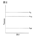
本開示のいくつかの実施形態では、図2に示されるように、出発p型ウエハは比較的に低い酸素濃度を有するので、ウエハがサーマルドナー形成アニール(例えば、1〜2時間で約400℃〜450℃)にさらされたときに、サーマルドナーの数(NTD)はアクセプタ(すなわちp型ドーパント)の数(Na)より少ない。このハンドルウエハは、p型ウエハ(N eff )として効果的に機能する。この点について、図2〜9においてアクセプタ(Na であり、時々Neff)は実線で示され、ドナー(Na であり、時々Neff)は点線で示されることに留意すべきである。また、ハンドルウエハの抵抗率が1/Neffに比例する(すなわちNeffが低いとき抵抗率は高く、その逆も同じである)ことも留意すべきである。 In some embodiments of the present disclosure, as shown in FIG. 2, since the starting p-type wafer will have a relatively low oxygen concentration, the wafer thermal donor formation anneal (e.g., about 1 to 2 hours 400 When exposed to (° C. - 450 ° C.), the number of thermal donors (N TD ) is less than the number of acceptors (ie, p-type dopants) (N a ). This handle wafer effectively functions as a p-type wafer (N eff ) . In this regard, (a N a, sometimes N eff) acceptor in FIG 2-9 is indicated by a solid line, (a N a, sometimes N eff) donor should be noted that indicated by dotted lines. It should also be noted that the resistivity of the handle wafer is proportional to 1 / N eff (ie, the resistivity is high when N eff is low and vice versa).
本開示によれば、図3に示されるように、ハンドルウエハ内に不均一な酸素分布を形成するように、サーマルドナー形成アニールに先立って、酸素の内方拡散によって高抵抗率領域が図2のウエハ内に形成されてもよい。ハンドルウエハの表面付近の領域の付加的な酸素は、この領域に形成されるサーマルドナーの数を増加させる。サーマルドナーのこの増加は、サーマルドナーの数をアクセプタの数と実質的に等しくなるようにし、これによりこの領域内のウエハを補償し、抵抗率を上昇させる。図3から分かるように、Neffは表面領域付近で0に近づき、後述する図10に示すピーク抵抗率値と似たピーク抵抗率をもたらす。これにより、これに関して、拡散酸素の酸素濃度が高いところでは、追加的なサーマルドナーはウエハ内にpn接合の形成をもたらし、補償は、pn接合で達成される。本開示の目的のために、“pn接合”は、(1)サーマルドナーおよびn型ドーパントの合計と(2)p型ドーパントと、の間の補償の結果として生じる接合であることに留意すべきである。図3のウエハのいくつかの実施形態では、ハンドルウエハの表面に向かって進むと、ハンドルウエハの前面においてサーマルドナーがアクセプタの数を超えない(すなわち、表面においてアクセプタは実質的にサーマルドナーの数と等しい、または超える)ような割合(増加率)で、サーマルドナーの数は増加してもよい。このような実施形態では、pn接合はウエハ内に形成されないが、抵抗率は表面に向かって増加し、図3に示すように、表面から離れたところよりもむしろ表面においてピーク抵抗率が達成される。 According to the present disclosure, as shown in FIG. 3, so as to form a non-uniform oxygen distribution in the handle wafer, prior to the thermal donor formation annealing, the high resistivity region by inward diffusion of oxygen is 2 May be formed in the wafer. The additional oxygen in the region near the surface of the handle wafer increases the number of thermal donors formed in this region. This increase in thermal donors, the number was to be substantially equal to the number of acceptor thermal donors, This ensures to compensate for wafer in this region, to increase the resistivity. As can be seen from FIG. 3, N eff approaches 0 near the surface region, resulting in a peak resistivity similar to the peak resistivity value shown in FIG. Thereby, in this regard, where the oxygen concentration of the diffuse oxygen is high , the additional thermal donor results in the formation of a pn junction in the wafer, and compensation is achieved at the pn junction. For the purposes of this disclosure, "pn junction" is to be noted that a joint resulting from compensation between, and (1) Total thermal donors and n-type dopant and (2) p-type dopant It is. In some embodiments of the wafer of FIG. 3, proceeds toward the surface of the handle wafer, the thermal donor does not exceed the number of acceptors in front of the handle wafer (i.e., the acceptor on the surface number of the substantially thermal donor The number of thermal donors may increase at a rate (increase rate ) such that In such an embodiment, the pn junction is not formed in the wafer, the resistivity increases toward the surface, as shown in FIG. 3, the peak resistivity at the surface rather than away from the surface achievement Is done.
本開示のいくつかの実施形態では、図4に示すように、高抵抗率領域は、p型のハンドルウエハにn型のドーパント量をドープすることにより、p型のハンドルウエハ内に作られてもよく、ドープは通常はハンドルウエハの前面を通して生じる。通常は、表面ドーピングは、ハンドルウエハの表面にn型のドーパントのピーク濃度を引き起こし、濃度はハンドルウエハの内部に向かって低下する。このドーパントプロファイルはp型のドーパントを補償する。いくつかの実施形態では、ドーパントの補償は、表面を反転して、ハンドルウエハ内でpn接合の形成を引き起こすほど十分に高くてもよい。ウエハ内の離れたところで、n型のドーパント(すなわち、ドナー)とp型のドーパント(すなわち、アクセプタ)の数は、実質的に等しくなり(すなわち、pn接合において)、補償とハンドルウエハ内のピーク抵抗率とを引き起こす。いくつかの実施形態では、ウエハ内のp型ドーパントおよびn型ドーパントの数は、ハンドルウエハの表面において実質的に等しく、表面に生じるピーク抵抗率をもたらす。 In some embodiments of the present disclosure, as shown in FIG. 4, a high resistivity region is created in a p-type handle wafer by doping a p-type handle wafer with an n-type dopant amount. even better, the dope usually occurs in through the front of the handle wafer. Normally, surface doping, the peak concentration of n-type dopant pull to Oko on the surface of the handle wafer, the concentration decreases toward the interior of the handle wafer. This dopant profile compensates for p-type dopants. In some embodiments, the compensation of the dopant inverts the surface, it may be sufficiently high enough to cause formation of a pn junction in the handle wafer. At a distance in the wafer, the number of n-type dopants (ie, donors) and p-type dopants (ie, acceptors) are substantially equal (ie, at the pn junction), and compensation and peaks in the handle wafer Cause and resistivity. In some embodiments, the number of p-type and n-type dopants in the wafer is substantially equal at the surface of the handle wafer, resulting in a peak resistivity occurring at the surface.
図4はサーマルドナーを説明(account for)していないことを留意すべきである。いくつかの実施形態では、ハンドル内の酸素濃度は、補償が達成される点に影響を及ぼすほど十分に高い。これに関して、サーマルドナーおよびn型ドーパントは、両方とも電子供与体として追加的な効果を有する。図5は、図4に似ているウエハプロファイルを示すが、図5のプロファイルはサーマルドナーの存在を示している。図5に示されるように、サーマルドナーおよびn型のドーパントの追加的な効果は、ハンドルウエハの前面において抵抗率を低下させ、図4と比べてハンドルウエハの表面から離れたピーク抵抗率を生じる。いくつかの実施形態では、酸素濃度はごく少量のサーマルドナーを形成する程度に十分に低く、ウエハは、サーマルドナーが抵抗率のプロファイルに著しく影響を及していない図4のハンドルウエハのように機能すると理解されるべきである。 It should be noted that FIG. 4 does not account for thermal donors. In some embodiments, the oxygen concentration in the handle, sufficiently high impact in that the compensation is achieved. In this regard , both thermal donors and n-type dopants have an additional effect as electron donors. FIG. 5 shows a wafer profile similar to FIG. 4, but the profile of FIG. 5 shows the presence of a thermal donor. As shown in FIG. 5, the additional effect of the thermal donor and n-type dopant reduces the resistivity at the front surface of the handle wafer, resulting in a peak resistivity away from the surface of the handle wafer compared to FIG. . In some embodiments , the oxygen concentration is low enough to form a very small amount of thermal donor , and the wafer is like the handle wafer of FIG. 4 where the thermal donor does not significantly affect the resistivity profile. It should be understood to function.
いくつかの実施形態では、図6に示すように、サーマルドナー形成アニール後にハンドルウエハ内に形成するサーマルドナーは、比較的に高い酸素濃度によってp型ドーパントの数を上回る。その結果、図6のハンドルウエハは、実際上はn型ウエハとして機能する。本開示の実施形態によれば、高抵抗率領域(特にこのような領域内のピーク抵抗率)は、不均一な酸素の分布を形成するように、ハンドルウエハの前面を通ってハンドルウエハから酸素の外方拡散すること(後述にて詳細を説明する)によって図6のウエハ内に形成されてもよく、その結果として図7に示すようなサーマルドナーをもたしてもよい。外方拡散処理は、ハンドルウエハの表面付近でのより少ないサーマルドナーの形成をもたらし、そのことでウエハは表層内で補償されるようになり、それにより表面付近に(または表面そのものに)ピーク抵抗率を形成する。n型のドーパントは、追加的なn型ドーパントを相殺して補償を達成するために追加的な酸素の外方拡散を必要とするので、図6のp型のウエハは、特にウエハの表層においては、p型のドーパントに加えてn型のドーパントでドープされないことが好ましいことに留意するべきである。 In some embodiments, as shown in FIG. 6, thermal donors that form in the handle wafer after the thermal donor formation anneal is greater than the number of the relatively high oxygen concentration thus p-type dopant. As a result, the handle wafer of FIG. 6 actually functions as an n-type wafer. According to embodiments of the present disclosure, the high resistivity region (especially the peak resistivity of such regions), so as to form a non-uniform distribution of oxygen, the front surface of the handle wafer from the handle wafer I through to outward diffusion of oxygen may be formed within the wafer of FIG. 6 me by the (described later in detail with below), may have a thermal donor as shown in FIG. 7 as a result . Outward diffusion process results in the formation of fewer thermal donor in the vicinity of the surface of the handle wafer, the wafer is turned so that compensated in the surface layer in that it, thereby (or surface itself) in the vicinity of the surface peak resistance Forming rate. Since n-type dopant, require outward diffusion of additional oxygen in order to make us compensation offset the additional n-type dopants, p-type wafer of FIG. 6, in particular the surface of the wafer in should be noted it is preferable that in addition to the p-type dopant is not doped with n-type dopant.
いくつかの実施形態では、図6に示すように、p型のウエハは、その中に比較的均一なp型のドーパント濃度を備えるp型のウエハであった。しかしながら、ウエハは、その前面を通して(例えば、アルミニウムなどのp型の不純物をドライブインすることにより)追加的なp型のドーパントでドープされた。図8に示すように、ウエハが比較的多数のサーマルドナーを含む場合(すなわち、サーマルドナーがp型ドーパントを上回る場合)、pn接合は、その後に続くサーマルドナー形成アニール後にハンドルウエハの表面付近でサーマルドナーの数(N TD )が減少するようにウエハから酸素を外方拡散することによって、形成されてもよい。サーマルドナーの数が最初からp型ドーパント(非表示)より少ない場合、酸素をウエハ内に内方拡散させてpn接合を作ってもよい。 In some embodiments, as shown in FIG. 6, p-type wafer, p-type and the Tsu wafer der with a dopant concentration of relatively uniform p-type therein. However, the wafer, through its front surface (e.g., by drive-in the p-type impurity such as aluminum) doped with additional p-type dopant. As shown in FIG. 8, if the wafer contains a relatively large number of thermal donors (ie, if the thermal donor exceeds the p-type dopant), the pn junction will be near the surface of the handle wafer after the subsequent thermal donor formation anneal. What I to outward diffusion of oxygen from the wafer as the number of thermal donors (N TD) is reduced, but it may also be formed. If the number of thermal donors is initially less than the p-type dopant (not shown) , oxygen may be diffused inward into the wafer to create a pn junction .
これに関して、p型の出発ハンドルウエハは、酸素の外方拡散、酸素の内方拡散、および/またはn型のドーピング、の任意の組み合わせを受けて、ハンドルウエハ内での補償と、その結果として補償領域付近で生じるピーク抵抗率と、を達成してもよいことが理解されるべきである。外方拡散、内方拡散および/またはドーピングの相対量は、このような補償を達成するのに十分であるべきであり、出発ハンドルウエハのp型のドーパント濃度および酸素濃度によって決まるべきである。ピーク抵抗率(すなわち、N eff の低下)は、図3、4、5、7および8では表面から離れたところに生じると示されているが、そのピークは表面そのもので生じてもよいことに留意するべきである。さらに特に指定がない限り、図2〜10におけるハンドルウエハの前面はy軸に相当することに留意するべきである。また、いくつかの実施形態では、p型またはn型のドーパント自体が、1つ以上のアニール工程の結果としてウエハから外方拡散してもよく、そしてこのドーパントの外方拡散は、当業者に認められているように、ウエハの抵抗率プロファイルに影響を及ぼしてもよいことも理解されるべきである。 In this regard , the p-type starting handle wafer is subjected to any combination of oxygen out-diffusion, oxygen in-diffusion , and / or n-type doping , resulting in compensation within the handle wafer and consequently a peak resistivity occurs near compensation region, it should be understood that there may be achieved. Out-diffusion, the relative amounts of inward diffusion and / or doping, such is that should be sufficient to compensate for us form, should depend dopant concentration and the oxygen concentration in the p-type of the starting handle wafer . Peak resistivity (i.e., reduction in N eff) is shown the results away from the surface in FIG. 3, 4, 5, 7 and 8, in that the peak that may occur in the surface itself It should be noted. Unless more specifically designated, the front surface of the handle wafer in FIG. 2-10 It should be noted that corresponding to the y-axis. Also, in some embodiments , the p-type or n-type dopant itself may diffuse out of the wafer as a result of one or more annealing steps , and the out-diffusion of this dopant is known to those skilled in the art. as has been observed, it should also be understood that may affect the resistivity profile of the wafer.
図2〜8のp型の出発ハンドルウエハは、不純物(たとえば、結晶融液内に存在した複数の不純物)としてウエハ内に存在する多数のn型ドーパントを含んでもよく、これらのドーパントはハンドルウエハの抵抗率プロファイルに影響を与え得ることに留意すべきである。さらに、後述する図9および10におけるn型の出発ハンドルウエハは、抵抗率プロファイルに影響を及ぼし得るp型のドーパントの不純物を含んでもよいことに留意すべきである。これに関し、本明細書で記載される“p型”の出発ハンドルウエハは、結晶が形成される時にn型のドーパントの不純物で補償されているもの考えられ、その逆もまた同様であると理解されるべきである。 The p-type starting handle wafer of FIGS. 2-8 may include a number of n-type dopants present in the wafer as impurities (eg, a plurality of impurities present in the crystal melt), and these dopants may be included in the handle wafer. It should be noted that the resistivity profile can be affected. Further, n-type starting handle wafer in FIGS. 9 and 10 will be described later, it includes a resistivity profile in the impurity of the p-type dopant capable of affecting it should be noted that it may be. In this regard, the starting handle wafer is being "p-type" as used herein is crystal n-type is compensated by the impurity dopants considered shall Tei when formed, and vice versa understood It should be.
・n型出発ハンドルウエハ
n型出発ハンドルウエハ(すなわち、バルク全体に渡ってn型のドーパントを備えたウエハ)は、補償によって高抵抗率領域を作るようにウエハのサーマルドナープロファイルを単独で操作できないので、p型の出発ハンドルウエハとは異なる。高抵抗率領域は、1つ以上のp型ドーパントによってウエハをドーピングすることにより、n型の出発ウエハ内に形成されてもよい。例えば図9に示すように、ハンドルウエハは、出発時のn型のドーパント濃度(Nd)と、サーマルドナーの数(NTD)とを有する。図10に示されるように、高抵抗率領域は、多数のp型のドーパント(Na)を、ウエハの表面を通してウエハにドーピングすることにより、図9のハンドルウエハ内に形成されてもよい。p型のドーパントは、n型のハンドルウエハ内に、ウエハの抵抗率が増加する高い補償領域を作り出すpn接合の形成をもたらす。
・ N-type starting handle wafer
n-type starting handle wafer (i.e., a wafer having an n-type dopant over the entire bulk), because can not operate the thermal donor profile of the wafer to create a high resistivity region by the compensation alone, p-type Different from the starting handle wafer. The high resistivity region may be formed in the n-type starting wafer by doping the wafer with one or more p-type dopants. For example, as shown in FIG. 9, the handle wafer has a dopant concentration of n-type at the time of starting (N d), and the number of thermal donors (N TD). As shown in FIG. 10, a high resistivity region may be formed in the handle wafer of FIG. 9 by doping the wafer with a number of p-type dopants (N a ) through the surface of the wafer. p-type dopant, into n-type handle wafer, to cod also the formation of a pn junction to create a high compensation region where the resistivity of the wafer is increased.
n型の出発ハンドルウエハへの酸素の外方拡散または内方拡散だけでは、通常はハンドルウエハ内に高抵抗率プロファイルを形成することはできないが、外方拡散および/または内方拡散の工程は、ハンドルウエハの抵抗率プロファイルに影響を及ぼし得ることに留意すべきである。例えば、ハンドルウエハの表面からの酸素の外方拡散は、ウエハ表面におけるサーマルドナーの数を減少し、それにより、高い補償領域を形成するのに使われるp型のドーパント数を低減する。さらに、酸素がウエハ内に内方拡散された場合、ウエハ内のピーク抵抗率を形成するためには、比較的多数のp型ドーパントが必要とされる。 Although out-diffusion or in-diffusion of oxygen only into an n-type starting handle wafer usually does not create a high resistivity profile in the handle wafer, It should be noted that the process can affect the resistivity profile of the handle wafer. For example, outward diffusion of oxygen from the surface of the handle wafer is to reduce the number of thermal donors in the wafer surface, thereby reducing the p-type number of dopants used to form the high compensation region. Furthermore, when oxygen is diffused inward into the wafer, a relatively large number of p-type dopants are required to form the peak resistivity in the wafer .
これに関して、n型の出発ハンドルウエハは、ハンドルウエハ内に高抵抗率領域を形成するために、p型ドーピング、酸素の外方拡散、または酸素の内方拡散、の任意の組み合わせを受けてもよいことが理解されるべきである。p型のドーピングは、ウエハ内に高い補償領域を形成するのに十分であるべきであり、出発ハンドルウエハのn型ドーパントの濃度および酸素濃度によって決まるべきである。図10のピーク抵抗率は、表面から離れたところに生じると示されているが、そのピークは表面そのもので生じてもよいことに留意すべきである。 In this regard, n-type starting handle wafer, to form a high resistivity region in the handle wafer, p-type doping, the oxygen outdiffusion, or inward diffusion of oxygen, even when subjected to any combination of It should be understood that it is good. p-type doping should be sufficient to form a high compensation region in the wafer, it should depend concentration and the oxygen concentration in the n-type dopant of the starting handle wafer. Peak resistivity of Figure 10 is Ru Tei shown to occur away from the surface, the peak should be noted that may occur in the surface itself.
・酸素の内方拡散および外方拡散の方法とサーマルドナーの形成
上述のように、本開示のいくつかの実施形態では、出発ハンドルウエハへの酸素の内方拡散または外方拡散は、その抵抗率プロファイルに影響を及ぼすのに望ましい。これに関して、酸素の内方拡散および外方拡散を達成するように、当業者に知られたいくつかの方法が使用されてもよい。本開示のいくつかの実施形態では、酸素の内方拡散または外方拡散は、さらに後述するように、酸素の内方拡散または外方拡散に都合のよい一連の処理条件の下で、ウエハをアニールすることにより達成される。
Methods of oxygen in- and out-diffusion and formation of thermal donors As noted above, in some embodiments of the present disclosure, in-diffusion or out-diffusion of oxygen into the starting handle wafer is its resistance. Desirable to affect rate profile. In this regard , several methods known to those skilled in the art may be used to achieve oxygen in-diffusion and out-diffusion. In some embodiments of the present disclosure, oxygen in- or out-diffusion is performed on the wafer under a series of processing conditions convenient for oxygen in-diffusion or out-diffusion, as further described below. This is achieved by annealing.
ハンドルの前面が酸素の影響を受けていない(例えば、その上に配置される自然酸化膜などの酸化物層が存在しない)実施形態、および表面が酸素を含む(例えば、自然酸化膜またはSOI製造後の誘電体層などの酸化物層がハンドルウエハの前面に存在する)実施形態において、酸素は、ハンドルウエハから外方拡散されてもよい。酸化物層がない実施形態では、比較的酸素の影響を受けない環境(例えば、約100ppmに満たない)でウエハを加熱することにより、酸素はハンドルウエハの前面から外方拡散され得る。このような実施形態では、外方拡散は、周囲環境より高い任意の温度で生じてもよく、より高い温度は、より速い外方拡散速度に相当する。ハンドルが表面の酸化物層を含まない実施形態において、外方拡散のアニールが実行されるのに適切な環境は、例えば、実質的にシリコンと不活性のガス(例えば、希ガス)および水素ガスを含む。 Embodiments where the front face of the handle is not affected by oxygen (eg, there is no oxide layer, such as a native oxide film disposed thereon), and the surface contains oxygen (eg, native oxide or SOI manufacturing) in the oxide layer is present on the front surface of the handle wafer) embodiment such as a dielectric layer after the oxygen may be out-diffused from the handle wafer. In the oxide layer is not an embodiment, a relatively oxygen insensitive environment (e.g., about less than 100 ppm) by heating the wafer, the oxygen may be outdiffusion from the front of the handle wafer. In such embodiments, the out-diffusion may occur at any temperature above ambient, higher temperatures correspond to faster outward diffusion rate. In embodiments where the handle does not include a surface oxide layer, the appropriate environment for the annealing of the outward diffusion is performed, for example, substantially silicon and inert gas (e.g., rare gas) and hydrogen gas including.
ハンドルウエハがその表面に酸化物層を有する実施形態では、ウエハを、酸素の平衡溶解度限界Oequilがバルク酸素の濃度Oiよりも小さくなる温度でアニールすることにより、酸素が外方拡散され得る。別の言い方をすれば、通常は、アニールの温度は、平衡酸素濃度Oequilがバルク酸素の濃度Oiと等しくまたは超える温度よりも、低くなるように維持されるべきである。大気中の酸素の許容量は、アニールの温度に依存してもよく、逆に、アニールの温度が、大気中の酸素量を考慮して選択されてもよいことに留意すべきである。ウエハの表面に酸化物層がある場合、環境の酸素含有量は大きく変化させることができ、適切な環境は、例えば、不活性ガス、水素および酸素を含む。 In embodiments the handle wafer having an oxide layer on its surface, a wafer, by the equilibrium solubility limit O equil oxygen anneals at becomes smaller temperature than the concentration O i of bulk oxygen, oxygen may be outdiffusion . In other words, usually, the temperature of annealing, than the equilibrium oxygen concentration O equil equals or exceeds the concentration O i of bulk oxygen temperature should be maintained to be lower. It should be noted that the amount of oxygen in the atmosphere may depend on the temperature of the anneal, and conversely , the temperature of the anneal may be selected taking into account the amount of oxygen in the air. If there is an oxide layer on the surface of the wafer, the oxygen content of the environment can vary greatly and suitable environments include, for example, inert gases, hydrogen and oxygen.
ハンドルウエハがその前面上に表面酸化物を含むかどうかに関わらず、外方拡散のアニールの時間は、ハンドルウエハの前面から、ウエハ内への酸素の拡散が望まれる位置までの深さによって決まる。好ましくは、アニールは少なくとも約10分間の長さ、または少なくとも30分、少なくとも1時間、少なくとも2時間もしくは少なくとも4時間である(例えば、約10分から約6時間)。酸素プロファイルも、SOI製造方法(例えば、約1100℃〜約1125℃での約1〜4時間のアニールなどの、高温の貼り合わせアニール(bond anneal))および/または電子デバイス製造方法の一部として生じるサーマルアニール(thermal anneal)によって影響を及ぼされ得ることに留意するべきである。さらに、外方拡散のアニール自体が、このような製造方法中に起こるアニールであってもよい。 Handle wafer regardless of whether they contain surface oxides on its front surface, the annealing time of the out-diffusion from the front surface of the handle wafer, diffusion of oxygen into the wafer by the depth of up to Nozomu Murrell position Determined. Preferably, the anneal is at least about 10 minutes long, or at least 30 minutes, at least 1 hour, at least 2 hours or at least 4 hours (eg, from about 10 minutes to about 6 hours). The oxygen profile may also be part of an SOI manufacturing method (eg, high temperature bond anneal, such as about 1 to 4 hours annealing at about 1100 ° C. to about 1125 ° C.) and / or electronic device manufacturing methods. It should be noted that it can be influenced by the resulting thermal anneal. Furthermore, the out-diffusion anneal itself may be an anneal that occurs during such a manufacturing method.
通常は、アニールの時間およびアニールの温度は、ハンドルウエハの表面領域で高抵抗率領域を十分に形成するように(例えば、ピーク抵抗率が概ね接合部に生じるか、またはハンドルウエハの前面に向かってウエハがますます補償されるような、pn接合)選択されるべきである。これに関して、これらのパラメータは、ウエハが、バルクウエハのドーパントの型と異なる型のドーパントによってもドープされるかどうか(例えば、p型ハンドルウエハがウエハの前面を通してn型ドーパントによりドープされるかどうか、またはその逆の状況でドープされるかどうか)に依存してもよく、また、出発ハンドルウエハの酸素含有量に依存してもよいことに留意するべきである。 Typically , the annealing time and annealing temperature are sufficient to form a high resistivity region at the surface area of the handle wafer (e.g., the peak resistivity generally occurs at the junction or toward the front surface of the handle wafer). So that the wafer is increasingly compensated ( pn junction). In this regard, these parameters, the wafer is doped with whether (eg, n-type dopant p-type handle wafer and through the front surface of the wafer is also doped with a dopant of a type different from the type of the dopant bulk wafer whether or may depend on whether the dope) in the context of the reverse, also, it should be noted that may be dependent on the oxygen content of the starting handle wafer.
酸素の内方拡散に関して、表面に酸化物を形成し(例えば、自然酸化物またはSOI製造後の誘電体層)、そして平衡酸素濃度Oequialがバルク酸素濃度Obulkを超える温度まで加熱することにより、酸素は、ウエハの前面を通して内方拡散されてもよい。これに関して、アニール温度は、酸素の平衡濃度Oequialがバルク濃度Obulkと実質的に等しくなる温度よりも、高くなるべきである。酸素を含む大気中でのアニールによるそれ自体のアニールの間、例えば、表面酸化物層はウエハの表面上に形成されてもよいことに留意すべきである。様々な実施形態において、内方拡散のアニールは少なくとも約10分の長さ、または約30分、少なくとも約1時間、少なくとも約2時間もしくは少なくとも約4時間(例えば、約10分から約6時間)である。 Respect inward diffusion of oxygen, to form an oxide on the surface (e.g., native oxide or SOI manufacturing after the dielectric layer), and the equilibrium oxygen concentration O Equial is by heating to a temperature above the bulk oxygen concentration O bulk , Oxygen may be diffused inward through the front surface of the wafer . In this regard, the annealing temperature, than the oxygen equilibrium concentration O Equial is bulk concentration O bulk substantially equal temperatures, should higher. It should be noted that during its own annealing by annealing in an atmosphere containing oxygen, for example, a surface oxide layer may be formed on the surface of the wafer. In various embodiments, the in-diffusion anneal is at least about 10 minutes long, or about 30 minutes, at least about 1 hour, at least about 2 hours, or at least about 4 hours (eg, from about 10 minutes to about 6 hours). is there.
上述の外方拡散の方法と同様に、通常は、アニールの気体中の酸素含有量(もしあれば)、内方拡散のアニールの時間およびアニールの温度は、ハンドルウエハの表面領域内に高抵抗率領域を十分に形成するように選択されるべきである。これらのパラメータは、ウエハもバルクウエハのドーパントの型とは異なる型のドーパントによりドープされるかどうかに依存してもよく、出発ハンドルウエハ酸素含有量と所望の抵抗層の厚さに依存してもよい。 Similar to the out-diffusion method described above, the oxygen content (if any) in the annealing gas, the in-diffusion annealing time, and the annealing temperature are typically high resistance in the surface area of the handle wafer. the rate region should be selected to sufficiently formed. These parameters wafer may be dependent on whether doped with different types of dopants also the type of dopant bulk wafer, be dependent on the desired thickness of the resistive layer and the starting handle wafer oxygen content Good.
酸素外方拡散のアニールおよび酸素内方拡散のアニールについて上述で列挙した処理条件(the process conditions)は例示であり、上述以外の条件が使用されてもよいことに留意すべきである。ハンドルウエハ内で所望の抵抗率プロファイルが得られるように、パラメータの任意の組み合わせが選択されてもよい。これに関して、このようなパラメータの選択は概して当業者の有する技術の範囲内であり、例えば、日常の実験を通じて経験的に決定してもよい。 Oxygen outward diffusion annealing and oxygen inward diffusion annealing for the listed processing conditions in the above (the process conditions) is illustrated, it should be noted that the conditions other than the above may be used. Any combination of parameters may be selected to obtain a desired resistivity profile in the handle wafer. In this regard, the selection of such parameters Ri generally Oh within the scope of the technical possessed by those skilled in the art, for example, it may be empirically determined through routine experimentation.
酸素の内方拡散に望まれる実施形態(例えば、p型のウエハ内にサーマルドナーを形成する)において、サーマルドナーは、サーマルドナーを形成するように格子間酸素が凝集するサーマルドナー形成アニールを実行することにより、形成されてもよい。これに関して、本明細書における“サーマルドナー”という言葉の使用は、いかなる特定の構造にも限定されるべきではない。このようなサーマルドナーは、例えば、酸素の凝集(例えば、少なくとも2つまたは3つの酸素原子の凝集)を含んでもよい。 In embodiments where oxygen in-diffusion is desired (eg, forming a thermal donor in a p-type wafer), the thermal donor performs a thermal donor formation anneal in which interstitial oxygen aggregates to form a thermal donor. By doing so, it may be formed. In this regard , the use of the term “thermal donor” herein should not be limited to any particular structure. Such thermal donors may include, for example, oxygen aggregation (eg, aggregation of at least two or three oxygen atoms).
本開示の様々な実施形態において、サーマルドナー形成アニールは少なくとも約350℃の温度で実行される。約550℃を超える温度は、サーマルドナーを格子間酸素に再び分離してしまうので、通常は、サーマルドナー形成アニールは約550℃より低い温度で実行される。いくつかの実施形態では、サーマルドナーが形成され、それからSOI形成またはRF処理などのその後の処理によって分離される。このような実施形態では、2回目のサーマルドナー形成アニールは、ハンドルウエハ内にサーマルドナーを形成するように実行されてもよい(すなわち、550℃を超える全ての処理工程が実行された後、サーマルドナー形成アニールが実行されてもよい)。 In various embodiments of the present disclosure, the thermal donor formation anneal is performed at a temperature of at least about 350 ° C. Typically, thermal donor formation anneals are performed at temperatures below about 550 ° C., since temperatures above about 550 ° C. will again separate the thermal donor into interstitial oxygen. In some embodiments, thermal donors are formed and subsequently processing the thus separated such that the SOI formation or RF processing. In such an embodiment , a second thermal donor formation anneal may be performed to form a thermal donor in the handle wafer (ie, after all processing steps above 550 ° C. have been performed, A donor formation anneal may be performed).
サーマルドナー形成アニールは、少なくとも約5分間、または少なくとも10分間、少なくとも30分間もしくは少なくとも約1時間(例えば、約5分間から約5時間、約5分間から約3時間または約30分から約3時間)行われてもよい。通常は、サーマルドナー形成アニールは、いかなる環境で行われてもよい。例示的な環境は、例えば、希ガス(例えば、アルゴン)、窒素、酸素、水素およびこれらの気体の組み合わせを含む。 The thermal donor formation anneal is at least about 5 minutes, or at least 10 minutes, at least 30 minutes or at least about 1 hour (eg, from about 5 minutes to about 5 hours, from about 5 minutes to about 3 hours, or from about 30 minutes to about 3 hours) It may be done. In general , the thermal donor formation anneal may be performed in any environment. Exemplary environments include, for example, noble gases (eg, argon), nitrogen, oxygen, hydrogen, and combinations of these gases.
サーマルドナー形成アニールは、SOI製造方法の部分を形成してもよく、および/またはRF回路製造方法の部分を形成してもよいことに留意すべきである。通常は、ハンドルウエハが約350℃から約550℃まで加熱され、およびその後の解離事象が生じない任意の方法(例えば、ウエハが約550℃を超えて加熱される方法)が適している。サーマルドナー形成アニールがデバイスの製造方法(例えば、RF製造方法)の一部を形成するいくつかの実施形態では、SOI構造体のハンドルウエハは、このような製造方法に先立って、その後のサーマルドナー形成アニール後にハンドルウエハが表層にpn接合を形成できるように(または、他の実施形態のように、ハンドルウエハの前面にピーク濃度を形成するように)、表層に酸素濃度プロファイルを有してもよい。このようなSOI構造は、n型またはp型であってもよい(すなわち、n型ドーパントのみ、もしくはp型ドーパントの不純物濃度に満たない追加的な多数のp型ドーパントのみを含む、またはp型ドーパントのみ、もしくはn型ドーパントの不純物濃度に満たない追加的な多数のn型ドーパントのみを含む)。 It should be noted that the thermal donor formation anneal may form part of the SOI fabrication method and / or form part of the RF circuit fabrication method. In general , any method in which the handle wafer is heated from about 350 ° C. to about 550 ° C. and no subsequent dissociation events occur (eg, a method in which the wafer is heated above about 550 ° C.) is suitable. Manufacturing method for a thermal donor formation annealing device (e.g., RF manufacturing method) In some embodiments forming part of the handle wafer of the SOI structure, prior to such a manufacturing method, subsequent thermal donor The handle wafer has an oxygen concentration profile on the surface so that the handle wafer can form a pn junction on the surface after the formation annealing (or so as to form a peak concentration on the front surface of the handle wafer as in other embodiments) . Also good. Such SOI structures may be n-type or p-type (i.e., n-type dopants only, or includes only additional number of p-type dopant is less than the impurity concentration of the p-type dopant, or p-type Including only the dopant or only a number of additional n-type dopants below the impurity concentration of the n-type dopant).
さらに、サーマルドナーは、n型出発ハンドルウエハ内にpn接合を形成することはできないが、n型ウエハが酸素の量を含み、かつサーマルドナー形成アニールがSOIまたはRF装置製造の一部として起こってもよいので、このようなサーマルドナーは典型的にこのようなウエハ内に付随的に形成する。このような処理の不可避的形成部分であるサーマルドナー形成アニールの結果として、本開示のいくつかの実施形態では、このような付随的に形成されるサーマルドナーのプロファイルを制御するように、酸素は外方拡散される。 Furthermore, the thermal donor is not able to form a pn junction with the n-type starting handle the wafer, n-type wafer comprises the amount of oxygen, and forming a thermal donor annealing occurred as part of a SOI or RF device manufacturing As such, such thermal donors are typically formed incidentally in such wafers. As a result of the thermal donor formation anneal is unavoidable forming part of such processing, in some embodiments of the present disclosure, so as to control the profile of such a concomitant thermal donors formed, oxygen Diffused outward.
これに関して、サーマルドナー形成アニールが実行される温度および実行される時間の長さが、サーマルドナープロファイルに影響を及ぼしてもよく、より高い温度およびより長いアニールにより、比較的多いサーマルドナーが形成されることに留意すべきである。温度およびアニールの時間は、酸素の外方拡散または内方拡散のパラメータと組み合わせて選択されるべきであり、いくつかの実施形態では、ウエハ内に所望の抵抗率プロファイルを作るようにドーパントプロファイルと組み合わせて選択されるべきである。概して、これらのパラメータの組み合わせの選択は当業者の有する技術の範囲内である。 In this regard, the length of time the thermal donor formation annealing is temperature and running is performed, may affect the thermal donor profile, the higher temperatures and longer annealing, relatively high thermal donor is formed that in particular it should be noted. Temperature and annealing time should be selected in combination with the parameters of the outdiffusion or inward diffusion of oxygen, in some embodiments, the dopant profile to produce a desired resistivity profile in the wafer Should be selected in combination. In general, the selection of combinations of these parameters is within the skill of one of ordinary skill in the art.
・pn接合を形成するハンドルウエハドーピング
上述のように、p型の出発ハンドルウエハは、多くの補償領域を形成するように、その前面を通して多数のn型のドーパントでドープされてもよく、ハンドルウエハまたはn型の出発ハンドルウエハの表層内のpn接合は、当該接合およびその結果としての高抵抗率領域を形成するように、多数のp型のドーパントでドープされてもよい。当業者にとって既知の任意の数の技術を利用して、ハンドルウエハに第2型のドーパントをドープしてもよい。例えば、出発ハンドルウエハは、ハンドルウエハの前面に適用されるドーパント原子の注入(implantation)または“ドライブイン(driving in)”によってドープされてもよい。ドーパント原子は、ウエハの前面にドーパント原子を含む溶液に接触させることにより、もしくは液体金属ドーパントに接触させることにより、またはスパッタリングにより、ウエハの表面に適用されてもよい。適用したら、バルク内のドーパントの平衡溶解度が第2型のドーパントの濃度を超える温度まで、ウエハをアニールすることにより、第2型のドーパントがウエハにドライブインされてもよい。典型的なドーパント(例えば、ホウ素またはリン)については、ドライブインアニールは、少なくとも約900℃、少なくとも約1,000℃または少なくとも約1,100℃の温度で実行されてもよく、アニールの時間は少なくとも約15分間、少なくとも約30分間または少なくとも約1時間であってもよい。特定される温度およびアニール時間は単なる例示であり、他の温度およびアニール時間が制限無く用いられてもよいことに留意するべきである。
Handle wafer doping as described above to form a pn junction, p-type starting handle wafer so as to form a number of compensation regions may be doped with a number of n-type dopant through the front, The pn junction in the surface of the handle wafer or n-type starting handle wafer may be doped with a number of p-type dopants to form the junction and the resulting high resistivity region. Using known any number of techniques to one of ordinary skill in the art, a second-type dopant may be doped to the handle wafer. For example, the starting handle wafer may be doped by implantation of dopant atoms which is applied to the front surface of the handle wafer (Implantation) or "drive-in (driving in)". Dopant atoms by Rukoto the front of the wafer is contacted with a solution containing a dopant atom, or by Rukoto into contact with the liquid metal dopant, or by sputtering, it may be applied to the surface of the wafer. Once applied, the second type dopant may be driven into the wafer by annealing the wafer to a temperature where the equilibrium solubility of the dopant in the bulk exceeds the concentration of the second type dopant. For typical dopants (eg, boron or phosphorus), the drive-in anneal may be performed at a temperature of at least about 900 ° C., at least about 1,000 ° C. or at least about 1,100 ° C., and the time of annealing is It may be at least about 15 minutes, at least about 30 minutes, or at least about 1 hour. It should be noted that the temperatures and annealing times specified are merely exemplary and other temperatures and annealing times may be used without limitation.
これに関して、アニールは、ウエハにドーパントをドライブインする目的のために、既存の製造方法の一部を構成してもよく、単独で実施される独立したアニールである必要はないことが理解されるべきである。さらにドライブインアニールは、上述したサーマルドナー形成アニールと同じアニール工程中に起こってもよい。しかしながら、十分な量のドーパントの拡散をもたらすためには、独立したアニールが好ましいことに留意すべきである。本開示のいくつかの実施形態では、第2型のドーパントは独立した処理工程によりウエハの前面に適用されるのではなく、むしろウエハの表面上のこれらの第2型のドーパントは、1つ以上の既存の処理工程に起因する不純物であることに留意すべきである。このような表面の不純物を作るかもしれない例示的な処理工程は、例えば、ウエハ洗浄工程、およびウエハの前面が空気中の不純物にさらされる任意の工程(例えば、ハンドルウエハの表面にホウ素を積もらせるかもしれないクリーンルーム環境にさらすこと)を含む。 In this regard, the annealing for the purpose of driving in the dopants to the wafer, may constitute part of an existing manufacturing process, it need not be independent annealed is carried out solely be understood Should. Furthermore, drive-in annealing may occur during the same annealing step as the thermal donor formation annealing described above . However, it should be noted that an independent anneal is preferred to provide a sufficient amount of dopant diffusion . In some embodiments of the present disclosure, the second-type dopant is not Runode applied to the front surface of the wafer by an independent process, but rather these second-type dopant on the surface of the wafer, one or more It should be noted that the impurities are due to existing processing steps . Exemplary processing steps that may create such surface impurities include, for example, a wafer cleaning step and any step where the front side of the wafer is exposed to impurities in the air (e.g., loading the handle wafer surface with boron). Exposure to a clean room environment)
ドーピングの量は、ハンドルウエハ内にpn接合が形成されるように(または、いくつかの実施形態では、表面に向かってウエハがますます補償され、それによりピーク抵抗率を表面に作るようになるように)選択されるべきである。これに関して、ドーピングも、ハンドルウエハ内のサーマルドナーのプロファイルによって決まるだろう。さらに、ハンドルウエハがn型のハンドルウエハで(すなわち、ウエハの至る所で、n型のドーパントが比較的均一な濃度でドープされる)、前面を通してp型のドーパントによりドープされるいくつかの実施形態では、ハンドルウエハのバルク層に向かって概ね低下するp型のドーパントの濃度を有するウエハの表面付近で、一般的にp型のドーパントの濃度は、n型のドーパントの濃度を超える。p型のドーパントは、実質的にn型ドーパント(および、必要に応じてサーマルドナー)の数と等しくなる点Pequalまで、減少する。この点(または領域)では、ウエハは大いに(高度に)補償され、ピーク抵抗率をもたらす(Pequal に生じるか否かは、サーマルドナーの存在の有無により決まる)。ウエハ内のこの点を超えると、ドナーの濃度は、p型のドーパントの濃度を超える。ハンドルウエハがp型のハンドルウエハで、前面を通してn型のドーパントでドープされている実施形態では、通常は、n型ドーパントの濃度は、ウエハの表面付近ではp型ドーパントの濃度を上回り、点Pequalにおいて2つの型のドーパントの濃度が実質的に等しくなるまで、n型ドーパントの濃度はハンドルウエハのバルク層に向かって概ね低下する。Pequalからバルク層に進むと、p型ドーパントの濃度はn型ドーパントの濃度を概ね上回る。 The amount of doping is such that a pn junction is formed in the handle wafer (or in some embodiments , the wafer is increasingly compensated towards the surface, thereby creating a peak resistivity at the surface. Should be selected). In this regard, doping also, will depend on the thermal donor profile in the handle wafer. Further, some implementations in which the handle wafer is an n-type handle wafer (ie, n-type dopant is doped at a relatively uniform concentration throughout the wafer) and is doped with a p-type dopant through the front surface. In form, near the surface of the wafer having a p-type dopant concentration that generally decreases toward the handle wafer bulk layer, the concentration of the p-type dopant generally exceeds the concentration of the n-type dopant. p-type dopant is substantially n-type dopant (and, thermal donors if necessary) until the number of equal Kunar point P equal to decreases. At this point (or region), the wafer is highly (highly) compensated, resulting in peak resistivity ( whether or not it occurs at Pequal depends on the presence or absence of a thermal donor). Beyond this point in the wafer, the donor concentration exceeds the p-type dopant concentration. Handle wafer is a p-type handle wafer, in the embodiment is doped with n-type dopant through the front, usually, the concentration of n-type dopant is above the concentration of the p-type dopant near the surface of the wafer, The n-type dopant concentration generally decreases toward the handle wafer bulk layer until the concentration of the two types of dopants is substantially equal at the point Pequal . Proceeding from Pequal to the bulk layer, the concentration of the p-type dopant generally exceeds the concentration of the n-type dopant.
記載されたものとは別のn型およびp型のドーパントのそれぞれの濃度プロファイルが、限定されることなしに利用されてもよいことに留意するべきである。例えば、出発ハンドルウエハ内の第1型のドーパントは、ウエハの全体にわたって比較的均一として通常は記載される。しかし、出発ドーパントの濃度は、ハンドルウエハ内で変化してもよい。例えば、出発ハンドルウエハは、ウエハの表面からある距離D1だけ第1型のドーパントでドープされてもよい。一般的に、これらの実施形態では、第2型のドーパントは距離D2(D2はD1より小さい)だけウエハにドライブインされる。 Each concentration profile of the described another n-type and p-type dopant and things, it should be noted that it may be utilized without limitation. For example, the first type of dopant in the starting handle wafer is typically described as relatively uniform throughout the wafer. However, concentration of the starting dopant may be strange turned into in the handle wafer. For example, the starting handle wafer may be doped with a first type dopant by a distance D 1 from the surface of the wafer. Generally, in these embodiments, a second type of dopant distance D 2 (D 2 is D 1 less than) driven in to the wafer only.
・ハンドルウエハの抵抗率プロファイル
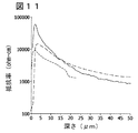
実施例1に従って調製された、いくつかのハンドルウエハの抵抗率プロファイルは、図11に示される。図11に示されるように、本開示のいくつかの実施形態よれば、ハンドルウエハは、ピーク抵抗率(Rpeak)がハンドルウエハの前面から離れて生じる抵抗率プロファイルを有する。しかし図11の抵抗率プロファイルは単なる例示であり、本開示の他の実施形態では、ウエハの表面においてピークが生じることを理解すべきである。表面から離れてピークが生じる実施形態では、Rpeakは表面(またはSOIウエハに組み込まれた場合には誘電体−ハンドル界面)から少なくとも約0.1μm、または表面から少なくとも約1μm、もしくは少なくとも約2μmで生じてもよい(例えば、約0.1μmから約15μm、約1μmから約15μm、約2μmから約10μm、約0.1μmから約5μmまたは約1μmから約5μm)。本開示のいくつかの実施形態では、ピーク抵抗率(Rpeak)は少なくとも約1,000ohm−cmであり、または他の実施形態においては少なくとも約2,000ohm−cm、少なくとも約5,000ohm−cm、少なくとも約7,500ohm−cm、少なくとも約10,000ohm−cmもしくは少なくとも約25,000ohm−cmである(例えば、約1,000ohm−cmから約100,000ohm−cm、約1,000ohm−cmから約50,000ohm−cm、約1,000ohm−cmから約25,000ohm−cmまたは約5,000ohm−cmから約25,000ohm−cm)。
Handle Wafer Resistivity Profiles The resistivity profiles of several handle wafers prepared according to Example 1 are shown in FIG. As shown in FIG. 11, according to some embodiments of the present disclosure, the handle wafer has a resistivity profile in which the peak resistivity (R peak ) occurs away from the front surface of the handle wafer. However the resistivity profile of Figure 11 is exemplary only, in other embodiments of the present disclosure, it should be understood that peaks in the surface of the wafer occurs. In embodiments where the peaks occur away from the surface, the R peak is at least about 0.1 μm from the surface (or dielectric-handle interface if incorporated into an SOI wafer), or at least about 1 μm from the surface, or at least about 2 μm. (Eg, about 0.1 μm to about 15 μm, about 1 μm to about 15 μm, about 2 μm to about 10 μm, about 0.1 μm to about 5 μm, or about 1 μm to about 5 μm). In some embodiments of the present disclosure, the peak resistivity (R peak ) is at least about 1,000 ohm-cm, or in other embodiments at least about 2,000 ohm-cm, at least about 5,000 ohm-cm. At least about 7,500 ohm-cm, at least about 10,000 ohm-cm, or at least about 25,000 ohm-cm (eg, from about 1,000 ohm-cm to about 100,000 ohm-cm, from about 1,000 ohm-cm About 50,000 ohm-cm, about 1,000 ohm-cm to about 25,000 ohm-cm, or about 5,000 ohm-cm to about 25,000 ohm-cm).
さらにこれに関して、ピーク抵抗率Rpeakとバルク抵抗率Rbulkとの抵抗率の差は、少なくとも約1,000ohm−cm、少なくとも約2,000ohm−cm、少なくとも約5,000ohm−cm、少なくとも約7,500ohm−cmまたは少なくとも約10,000ohm−cmであってもよい(例えば、約1,000ohm−cmから約75,000ohm−cm、約1,000ohm−cmから約25,000ohm−cm、約1,000ohm−cmから約15,000ohm−cmまたは約5,000ohm−cmから約25,000ohm−cm)。さらに、バルク抵抗率Rbulkに対するピーク抵抗率Rpeakの比率は、少なくとも約2:1、少なくとも約3:1、少なくとも約5:1または少なくとも約7:1であってもよい(例えば、約2:1から約100:1、約2:1から約75:1、約2:1から約50:1、約3:1から約50:1または約3:1から約25:1)。 Further in this regard , the resistivity difference between the peak resistivity R peak and the bulk resistivity R bulk is at least about 1,000 ohm-cm, at least about 2,000 ohm-cm, at least about 5,000 ohm-cm, at least about 7 , 500 ohm-cm, or at least about 10,000 ohm-cm (eg, from about 1,000 ohm-cm to about 75,000 ohm-cm, from about 1,000 ohm-cm to about 25,000 ohm-cm, about 1 5,000 ohm-cm to about 15,000 ohm-cm or about 5,000 ohm-cm to about 25,000 ohm-cm). Further, the ratio of peak resistivity R peak to bulk resistivity R bulk may be at least about 2: 1, at least about 3: 1, at least about 5: 1, or at least about 7: 1 (eg, about 2 1 to about 100: 1, about 2: 1 to about 75: 1, about 2: 1 to about 50: 1, about 3: 1 to about 50: 1, or about 3: 1 to about 25: 1).
ハンドルウエハはまた、その前面で抵抗率RHDを有し、SOI製造後に前面は誘電体層との界面を形成する。上述したように、いくつかの実施形態ではピーク抵抗率Rpeakは、表面/界面で生じる。このような実施形態では、RpeakはRHDに等しい。しかし、他の実施形態では、図11に示すように、抵抗率はRpeakからウエハの表面まで概ね減少する。これらの実施形態では、RHDに対するRpeakの比率は、少なくとも約2:1、少なくとも約3:1、少なくとも約5:1または少なくとも約7:1であってもよい(例えば、約2:1から約100:1、約2:1から約75:1、約2:1から約50:1、約3:1から約50:1または約3:1から約25:1)。いくつかの実施形態では、抵抗率Rpeakと抵抗率RHDとの抵抗率の差は、少なくとも約1,000ohm−cm、少なくとも約2,000ohm−cm、少なくとも約5,000ohm−cm、少なくとも約7,500ohm−cmまたは少なくとも約10,000ohm−cmであってもよい(例えば、約1,000ohm−cmから約75,000ohm−cm、約1,000ohm−cmから約25,000ohm−cm、約1,000ohm−cmから約15,000ohm−cmまたは約5,000ohm−cmから約25,000ohm−cm)。 The handle wafer also has a resistivity R HD on its front surface, which forms an interface with the dielectric layer after SOI fabrication. As noted above, in some embodiments , the peak resistivity R peak occurs at the surface / interface. In such embodiments, R peak is equal to R HD. However, in other embodiments, as shown in FIG. 11, the resistivity is generally reduced from R peak to the surface of the wafer. In these embodiments, the ratio of R peak to R HD may be at least about 2: 1, at least about 3: 1, at least about 5: 1, or at least about 7: 1 (eg, about 2: 1 To about 100: 1, about 2: 1 to about 75: 1, about 2: 1 to about 50: 1, about 3: 1 to about 50: 1, or about 3: 1 to about 25: 1). In some embodiments , the resistivity difference between resistivity R peak and resistivity R HD is at least about 1,000 ohm-cm, at least about 2,000 ohm-cm, at least about 5,000 ohm-cm, at least about May be 7,500 ohm-cm or at least about 10,000 ohm-cm (eg, about 1,000 ohm-cm to about 75,000 ohm-cm, about 1,000 ohm-cm to about 25,000 ohm-cm, about 1,000 ohm-cm to about 15,000 ohm-cm or about 5,000 ohm-cm to about 25,000 ohm-cm).
本開示の実施形態のハンドルウエハは概して、抵抗率がウエハバルク内のハンドルウエハの抵抗率を上回る高抵抗率領域を有する。本開示の目的で、ウエハバルクの抵抗率は、ウエハが、高抵抗率領域を作る本開示の方法(例えば、ウエハ内でのサーマルドナーの形成および第2型のドーパントの使用)を受ける前の、バルク内の平均抵抗率である。さらにこれに関して、本開示のいくつかの実施形態では、ウエハの抵抗率が、あるウエハの深さにおいてバルクの抵抗率を、バルクの抵抗率の少なくとも約50%上回るときに、高抵抗率領域が始まる(例えば、約2,000ohm−cmのバルク抵抗率を有するハンドルウエハの高抵抗率領域は、抵抗率が約3,000ohm−cmを上回る任意の軸領域(axial region)を含む)。他の実施形態では、あるウエハの深さにおけるウエハの抵抗率が、バルクの抵抗率を少なくとも約75%、少なくとも約100%、少なくとも約150%または少なくとも約200%上回るときに、高抵抗率領域が始まる。 The handle wafer of embodiments of the present disclosure generally has a high resistivity region where the resistivity exceeds the resistivity of the handle wafer in the wafer bulk. For purposes of this disclosure, the resistivity of the wafer bulk is determined before the wafer is subjected to the disclosed methods of creating a high resistivity region (eg, formation of a thermal donor in the wafer and use of a second type dopant). The average resistivity in the bulk. Further in this regard, in some embodiments of the present disclosure, the resistivity of the wafer, bulk resistivity at a depth of some wafer, when the above at least about 50% of the bulk resistivity, a high resistivity region beginning or Ru (e.g., a high resistivity region of the handle wafer having a bulk resistivity of about 2,000ohm-cm includes any axis area resistivity greater than about 3,000ohm-cm (axial region)) . In other embodiments, the high resistivity region when the resistivity of the wafer at a depth of the wafer is at least about 75%, at least about 100%, at least about 150% or at least about 200% greater than the bulk resistivity. There Ru started or.
本開示の実施形態のハンドルウエハの高抵抗率領域は、ハンドルウエハの前面からの深さDSLに延在するハンドルウエハの表面領域に生じる、として一般的に記載される。いくつかの実施形態では、ピークから表面に向かう抵抗率は、高抵抗率領域の閾値(例えば、バルク抵抗率より約50%大きい)を下回って、またはバルク自体の抵抗率を下回って低下するかもしれないので、本開示のハンドルウエハの高抵抗率領域は、ハンドルウエハの前面まで延在しないことに留意するべきである。したがって、高抵抗率領域は、この表層内に存在するが、ハンドルウエハの前面まで延在する必要がないと理解されるべきである。 High resistivity region of the handle wafer of an embodiment of the present disclosure, occurs in the surface region of the handle wafer that extends to a depth D SL from the front surface of the handle wafer, as is generally described. In some embodiments, the resistivity toward the surface from the peak threshold of the high resistivity region (e.g., about 50% greater than the bulk resistivity) below, or may be lowered below the resistivity of the bulk itself It should be noted that the high resistivity region of the handle wafer of the present disclosure does not extend to the front surface of the handle wafer. Thus, it should be understood that the high resistivity region exists in this surface layer but does not need to extend to the front surface of the handle wafer.
これに関して、表層の深さDSLは、ウエハの前面から(または、ハンドルウエハがSOI構造体に組み込まれた実施形態では、誘電体−ハンドル界面から)高抵抗率領域の最下点(すなわち、ウエハバルクと高抵抗率領域との間の界面)までの距離に概ね相当する。本開示の1つ以上の実施形態では、表面領域の深さDSLは少なくとも約5μm、少なくとも約10μm、少なくとも約15μm、少なくとも約20μmまたは少なくとも約25μmである(例えば、約5μmから約100μm、約5μmから約50μm、約5μmから約40μmまたは約10μmから約50μm)。ハンドルウエハは、表層からハンドルウエハの後面に延在するバルク層も含むことに留意すべきである。 In this regard, the surface layer of the depth D SL from the front surface of the wafer (or, in the embodiment the handle wafer has been incorporated into the SOI structure, the dielectric - from the handle interface) the lowest point of the high resistivity region (i.e., This corresponds approximately to the distance to the interface between the wafer bulk and the high resistivity region. In one or more embodiments of the present disclosure, the depth D SL at least about 5μm surface area of at least about 10 [mu] m, at least about 15 [mu] m, at least about 20μm, or at least about 25 [mu] m (e.g., from about 5μm to about 100 [mu] m, about 5 μm to about 50 μm, about 5 μm to about 40 μm, or about 10 μm to about 50 μm). It should be noted that the handle wafer also includes a bulk layer that extends from the surface layer to the rear surface of the handle wafer.
上述のように、抵抗率領域自体の厚さDresは、表層の深さDSLよりも小さくてもよい。本開示の様々な実施形態において、抵抗率領域の厚さDresは少なくとも約1μm、少なくとも約5μm、少なくとも約10μm、少なくとも約15μm、少なくとも約20μmまたは少なくとも約25μmである(例えば、約1μmから約100μm、約1μmから約50μm、約5μmから約40μmまたは約10μmから約50μm)。 As described above, the thickness D res of the resistivity region itself may be smaller than the depth D SL of the surface layer. In various embodiments of the present disclosure, the resistivity region thickness D res is at least about 1 μm, at least about 5 μm, at least about 10 μm, at least about 15 μm, at least about 20 μm, or at least about 25 μm (eg, from about 1 μm to about 25 μm). 100 μm, about 1 μm to about 50 μm, about 5 μm to about 40 μm, or about 10 μm to about 50 μm).
図11で示される抵抗率プロファイルおよび上述したプロファイルは、ハンドルウエハのSOI構造体への組み込み前、SOI構造体への組み込み後、またはSOI構造体の表面へのRF装置の形成後のハンドルウエハにおけるプロファイルであってもよいことに留意すべきである。これに関して、“下の”、“上の”、“1番上の”および/または“1番下の”という用語は限定された意味で考えられるべきでなく、これらの用語はハンドルウエハおよび/またはSOI構造体の任意の特定の方向を意味するように意図していないことが理解されるべきである。 Resistivity profile and profile described above is shown in Figure 11, prior to incorporation into SOI structure of a handle wafer, after incorporation into SOI structure, or to the handle wafer after the formation of the RF device to the surface of the SOI structure a definitive profile it should be noted that may be. In this regard , the terms “bottom”, “top”, “top” and / or “bottom” should not be considered in a limited sense; these terms include handle wafers and / or Or it should be understood that it is not intended to imply any particular orientation of the SOI structure.
サーマルドナー形成アニールが実行される(例えば、約2時間で約450℃のアニール)前に、またはこのようなサーマルドナー形成アニールの実行後に、(SOI製造の前または後の)ハンドルウエハは、上述の、および/または図(例えば、図11、15および/または16)に示される抵抗率プロファイルを有してもよい。さらに、本開示のいくつかの実施形態が、ハンドルウエハの“前面”に関して記載され、望ましい(複数の)特徴を有するハンドルウエハがSOI構造体に組み込まれてもよく、この“前面”は誘電体層との界面を形成することを理解されるべきである(すなわち、貼り合わせ工程の間および後で、誘電体−ハンドル界面を形成する)。本明細書で参照するハンドルウエハの“前面”は、概して“誘電体−ハンドル界面”と置き換え可能であり、“前面”という用語は限定的な意味で考えられるべきではない。 Thermal donor formation anneal is performed (e.g., about anneal to about 450 ° C. for 2 hours) before or after the execution of such thermal donor formation annealing, (before or after SOI manufacturing) handle wafer, above And / or a resistivity profile as shown in the figures (eg, FIGS. 11, 15 and / or 16). Furthermore, some embodiments of the disclosure have been described with respect to "front" of the handle wafer, preferably (s) feature may handle wafer is or write set in SOI structures having, this "front" is the dielectric It should be understood that it forms an interface with the body layer (ie, forming a dielectric-handle interface during and after the bonding process). The “front surface” of a handle wafer referred to herein is generally interchangeable with “dielectric-handle interface” and the term “front surface” should not be considered in a limiting sense.
・SOI構造体の製造
様々な実施形態における上述のハンドルウエハは、当業者に知られたいずれかのSOI構造体を形成するための方法に従ってSOI構造体に組み込みまれる。これに関して、当然ながら上述の1つ以上の処理工程がSOI製造方法の一部を形成してもよいことが理解されるべきである(例えば、サーマルドナー形成アニール、ドーパントの“ドライブイン”アニール等)。SOI構造体を形成するための例示的な方法は、ウエハ貼り合わせ工程(例えば、ドナーとハンドルウエハの少なくとも一方の表面に取り付けられた誘電体層と貼り合わせることと、エッチングおよび/または研磨、または切断によりドナーウエハの一部を除去すること)、および高温のアニールにより埋め込み酸素層に変換される損傷領域を形成するように酸素イオンがバルクシリコン基質に埋め込まれるSIMOX工程を含む。
Manufacturing of SOI structure The handle wafer described above in various embodiments is incorporated into an SOI structure according to any method for forming an SOI structure known to those skilled in the art. In this regard, it should of course above the one or more processing steps it is understood that may form part of the SOI manufacturing process (e.g., thermal donor formation annealing, dopant "drive-in" such as annealing ). Exemplary methods for forming SOI structures wafer bonding process (e.g., a possible bonded to the dielectric layer attached to at least one surface of the donor and the handle wafer, etching and / or polishing, or it removes part of Ri due to cleavage donor wafer), and a SIMOX process in which oxygen ions are implanted into a bulk silicon substrate to form a damaged region which is converted into the buried oxygen layer by high-temperature annealing.
上述の抵抗率プロファイルを有する(例えば、SOI製造前、SOI製造後または装置(例えば、RF装置)製造後に生じる所望の抵抗率プロファイルを有する)ハンドルウエハが使用されるウエハ貼り合わせ工程に従って作られたSOIウエハは、図12−14に示され、後述される。貼り合わせ工程では、ドナーとハンドルを一緒に貼り合わせる前に、ドナーウエハ、ハンドルウエハまたはその両方の表面に誘電体層が形成(例えば、蒸着または成長)されてもよい。これに関して、SOI構造体およびSOI構造体を調製する方法は、ドナーウエハ上に蒸着または成長させた誘電体層を有するとして、および誘電体層の表面に貼り合わせたハンドルウエハの表面を有するとして、本明細書に記載される。しかし、ドナーウエハ上への誘電体層の成長または蒸着の代わりに、またはそれに加えて、誘電体層はハンドルウエハ上に成長または蒸着してもよいこと、そしてこれらの構造体は、制限されることなく任意の様々な方法(arrangement)で貼り合わされてもよいことを理解されるべきである。本明細書で参照するハンドルウエハ上に個別に蒸着される誘電体層は、限定的な意味で考えられるべきではない。 Made according to a wafer bonding process in which a handle wafer having the above-described resistivity profile (eg, having a desired resistivity profile that occurs before SOI fabrication, after SOI fabrication, or after device (eg, RF device) fabrication) is used. The SOI wafer is shown in FIGS. 12-14 and will be described later. In the bonding process , a dielectric layer may be formed (eg, deposited or grown) on the surface of the donor wafer, the handle wafer, or both before bonding the donor and handle together. In this regard, as a method for preparing an SOI structure and SOI structure as having a dielectric layer deposited or grown on the donor wafer, and a surface of the handle wafer that has Awa adhered to the surface of the dielectric layer, Described herein. However, instead of the growth or deposition of a dielectric layer on the donor wafer, or in addition to, dielectric layers it may also be grown or deposited on the handle wafer Ikoto, and these structures is limited It should be understood that they may be joined in any of a variety of arrangements without . The dielectric layers individually deposited on the handle wafer referred to herein should not be considered in a limiting sense.
図12を参照して、誘電体層15(例えば、酸化ケイ素および/または窒化ケイ素の層)は、ドナーウエハ12の研磨された(polished)前面に形成(例えば、蒸着または成長)される。誘電体層15は当業者に既知の任意の技術に従って適用されてもよく、例えば、熱酸化(例えば、湿式酸化または乾式酸化)、化学蒸着またはこれらの技術の組み合わせ等である。ドナーウエハ12の前面にのみあるとして誘電体層が図12に示されるが、ハンドルウエハの全表面上に誘電体層が成長することがより実用的であることに留意すべきである。
Referring to FIG. 12, a dielectric layer 15 (eg, a layer of silicon oxide and / or silicon nitride) is formed (eg, deposited or grown) on the polished front surface of
一般的に言えば、誘電体層15は、最終的な構造体(final structure)に所望の絶縁特性を提供するのに十分な実質的に均一な厚さに成長する。しかし、典型的には、誘電体層は少なくとも約1nmと約5,000nm未満、約3,000nm未満、約1,000nm未満、約500nm未満、約300nm未満、約200nm未満、約150nm未満、約100nm未満または約50nm未満の厚みを有する。誘電体層15は、SOI構造体での使用に適する任意の電気的な絶縁材料をであってもよく、例えば、SiO2、Si3N4または酸化アルミニウム、窒化アルミニウムもしくは酸化マグネシウムを含む材料などである。1つの実施形態では、誘電体層15はSiO2である(すなわち、誘電体層は本質的にSiO2から成る)。
Generally speaking, the
これに関してSOI構造体は本明細書で誘電体層を有するとして記載されるが、いくつかの実施形態では、誘電体層が排除されてハンドルウエハとドナーウエハが“直接的に貼り合わされる”ことを理解されるべきである。このような誘電体層の本明細書の参照は、限定的な意味で考えられないべきである。このような直接貼り合わされた構造体を作るのに、当業者に知られた多数の技術の任意の1つが使われてもよい。 In this regard, although SOI structures are described herein as having a dielectric layer , in some embodiments , the dielectric layer is eliminated and the handle wafer and donor wafer are “directly bonded”. Should be understood. Reference herein to such a dielectric layer should not be considered in a limiting sense. Any one of a number of techniques known to those skilled in the art may be used to make such a directly bonded structure.
いくつかの実施形態では、イオン(例えば、水素原子、ヘリウム原子または水素およびヘリウム原子の組み合わせ)は、十分均一に規定された深さで、切断面17を規定するドナーウエハの前面の真下に注入される。イオンの組み合わせが注入される場合、イオンは同時に、または順次に注入されてもよいことに留意すべきである。イオン注入は当業者に知られた手段を用いて行われてもよい。例えばこの注入は、米国特許第6,790,747で開示される工程と同様の方法で行われてもよい。注入のパラメータは、例えば、約20〜約125keV(例えば、H2 +は20keVのエネルギー、2.4×10¹⁶ions/cm2)または約40〜約125keVの総エネルギーで、例えば、約1×1015ions/cm2から約1×1017のions/cm2(例えば、約1×1016ions/cm2から約7.5×1016ions/cm2)のイオン注入の総量を含んでもよい。イオンの組み合わせが使用される場合き、ドープ量(dose)はイオンの組み合わせの間で適宜調整されてもよい(例えば、He+が36keVのエネルギーで注入されてもよく、約1×1016ions/cm2の量のH2が続いて48keVのエネルギーおよび約5×1015ions/cm2の量が注入される。)
In some embodiments, the ion (e.g., hydrogen atom, a combination of helium atoms or hydrogen and helium atoms) has a sufficiently uniformly defined depth, is injected just under the front of the donor wafer to define a cutting
誘電体層の蒸着に先立って注入が実行されるとき、それに続くドナーウエハ上の誘電体層の成長または蒸着が、(ウエハ貼り合わせ処理工程より前に)早期分離(premature separation)またはドナー層の平面17に沿って切断するのを防止するのに十分な低温で適切に実行される。分離または切断の温度は、注入された種類、注入された量および注入された材料の複合関数である。しかし、一般的には早期分離または切断は、蒸着または成長温度を約500℃より低く維持することにより避けることができる。 When implantation is performed prior to the deposition of the dielectric layer, subsequent growth or deposition of the dielectric layer on the donor wafer may cause premature separation ( before the wafer bonding process ) or the plane of the donor layer. It is appropriately performed at a sufficiently low temperature to prevent the cut along the 17. The temperature of separation or cutting is a composite function of the type injected, the amount injected, and the material injected. However, in general, early separation or cutting it may Rukoto avoided by maintaining below about 500 ° C. The deposition or growth temperature.
次に、図33を参照すると、親水性接着工程を通して貼り合わされたウエハ20を形成するために(必要に応じて、その上に形成される誘電体層(例えば、酸化物層)を有してもよい)、誘電体層15の前面はそれからハンドルウエハ10の前面に貼り合わされる。誘電体層15とハンドルウエハ10は、ウエハの表面を、例えば酸素または窒素を含むプラズマに曝すことで貼り合わされてもよい。プラズマに曝すことは、しばしば表面活性化として参照される方法で表面の構造を修飾する。ウエハはそれから互いに押し付けられ、貼り合わせ界面18における貼り合わせが、それらの間に形成される。
Next, referring Then, in order to form a
貼り合わせに先立って、誘電体層およびハンドルウエハの表面は、当業者に知られた技術を用いて、その貼り合わせのための表面を調製するように、必要に応じて洗浄および/または簡単なエッチングまたは平坦化を受けてもよい。特定の理論にとらわれることなく、SOI構造体のシリコン表面の質は、一部分において、貼り合わせに先立つ表面の質の働きであると、一般的に考えられる。さらに、貼り合わせに先立つ両方の表面の質は、得られた貼り合わせ界面の質または強さに、直接的な影響を有する。 Prior to bonding, the surface of the dielectric layer and the handle wafer can be cleaned and / or simplified as necessary to prepare the surface for bonding using techniques known to those skilled in the art. it may receive etching or planarization. Without being bound by a particular theory, it is generally considered that the silicon surface quality of the SOI structure is, in part, a function of the surface quality prior to bonding. Furthermore, the quality of both surfaces prior to bonding, the quality or strength of the bonding interface obtained, having a direct influence.
ある場合は、それ故に、例えば、貼り合わせに先立って低い表面粗さ(例えば、0.5nm未満の二条平均平方根粗さ(RMS))を得るために、誘電体層および/またはハンドルウエハは1つ以上の次の手順を受けてもよく、(i)例えば、CMPによる平坦化、および/または(ii)例えば、親水性表面処理過程(例えば、約65℃で約20分間、例えば1:2:50の比率の水酸化アンモニウム、過酸化水素および水を含む溶液と表面が接触するRCA SC−1洗浄過程、その後の脱イオン水のすすぎ、乾燥)などの、湿式化学洗浄手順による洗浄である。一方または両方の表面はまた、得られた貼り合わせの強さを増加するために、湿式洗浄処理の後に、またはその代わりとして、必要に応じてプラズマ活性化を受けてもよい。プラズマ環境は、例えば、酸素、アンモニア、アルゴン、窒素、ジボランまたはホスフィンを含んでもよい。 In some cases, therefore, the dielectric layer and / or the handle wafer is 1 to obtain a low surface roughness (eg, double mean square roughness (RMS) less than 0.5 nm) prior to bonding, for example. One or more of the following procedures may be followed: (i) planarization by, eg, CMP, and / or (ii), eg, a hydrophilic surface treatment process (eg, at about 65 ° C. for about 20 minutes, eg, 1: 2 : RCA SC-1 cleaning process in which the surface is in contact with a solution containing ammonium hydroxide, hydrogen peroxide and water in a ratio of 50, followed by deionized water rinse, drying), etc. . One or both surfaces may also be used to increase the strength of the bonding obtained, after the wet cleaning process, or alternatively, may be subjected to a plasma activation as necessary. The plasma environment may include, for example, oxygen, ammonia, argon, nitrogen, diborane or phosphine.
一般的に言えば、ウエハの貼り合わせは、当業者に知られた任意の技術を基本的に用いて実行されてもよく、貼り合わせ界面の形成を達成するのに用いられる供給されるエネルギーは、確実に貼り合わせ界面の完全性(integrity)がその後の処理(すなわち、ドナーウエハ内の、切断面または分離面17に沿った分離による層転写)の間持続することができる十分な量である。しかし、一般的には、ウエハの貼り合わせは、大気圧または低下させた圧力(例えば、約50mTorr)で、室温と後に続く加熱により上昇した温度(例えば、少なくとも約200℃、少なくとも約300℃、少なくとも約400℃または少なくとも約500℃)で、十分な時間(例えば、少なくとも約10秒間、少なくとも約1分間、少なくとも約15分間、少なくとも約1時間または少なくとも約3時間)で、誘電体層とハンドルウエハの表面を(必要に応じて、その上の別の誘電体層と)接触させることにより達成される。例えば、加熱は約350℃で約2時間行われてもよい。結果としての界面は、約500mJ/m2より大きい、または約1000mJ/m2より大きい、約1500mJ/m2より大きい、または約2000mJ/m2より大きい貼り合わせ強度を有してもよい。上昇した温度は、ドナーウエハとハンドルウエハとの隣接する表面の間の共有結合の形成を引き起こし、そのようにしてドナーウエハとハンドルウエハとの間の結合を固める。貼り合わされたウエハの加熱またはアニールと同時に、ドナーウエハに早期に注入されたイオンは切断面を弱める。ドナーウエハの一部分はそれから、SOI構造体を形成するように、切断面に沿って貼り合わされたウエハから分離(すなわち切断)される。
Generally speaking, wafer bonding may be performed basically using any technique known to those skilled in the art, and the energy supplied to achieve the formation of the bonding interface is A sufficient amount to ensure that the integrity of the bonding interface can persist during subsequent processing (ie, layer transfer by separation along the cut or
貼り合わせ界面が形成された後、結果として生じる貼り合わされた界面は、ドナーウエハ(図14)内の分離または切断面に沿って裂け目を誘発するのに十分な状態にさらされる。一般的に言うと、この裂け目は当業者に知られた技術を用いて達成されてもよく、例えば、熱的および/または機械的に誘発される切断技術等である。しかし、一般的には、割裂(fracturing)は、少なくとも約200℃、少なくとも約300℃、少なくとも約400℃、少なくとも約500℃、少なくとも約600℃、少なくとも約700℃または少なくとも約800℃の温度(温度は、例えば、約200℃から約800℃、または約250℃から約650℃の範囲である)で少なくとも約10秒、少なくとも約1分間、少なくとも約15分間、少なくとも約1時間または少なくとも約3時間の時間(より高い温度はより短いアニール時間を必要とし、その逆も同様である)で、不活性(例えば、アルゴンまたは窒素)雰囲気または周囲の環境の下で、貼り合わされた構造をアニールすることにより達成される。 After the bonded interface is formed, the resulting bonded interface is exposed to conditions sufficient to induce a tear along the separation or cutting plane in the donor wafer (FIG. 14). Generally speaking, this tear may be achieved using techniques known to those skilled in the art, such as thermally and / or mechanically induced cutting techniques. Generally, however, fracturing is performed at a temperature of at least about 200 ° C., at least about 300 ° C., at least about 400 ° C., at least about 500 ° C., at least about 600 ° C., at least about 700 ° C. or at least about 800 ° C. Temperature ranges from, for example, about 200 ° C. to about 800 ° C., or about 250 ° C. to about 650 ° C.) for at least about 10 seconds, at least about 1 minute, at least about 15 minutes, at least about 1 hour, or at least about 3 Anneal the bonded structure under an inert (eg, argon or nitrogen) atmosphere or ambient environment for a period of time (higher temperatures require shorter anneal times and vice versa) Is achieved.
これに関して、別の実施形態では、この分離は、単独でまたはアニールに加えて機械力の手段により誘発または達成されてもよいことに留意すべきである。例えば、貼り合わされたウエハは、ドナーウエハの一部を貼り合わされたウエハから離れて引っ張るために、貼り合わされたウエハの反対面に対して垂直に機械力が適用される治具内に配置されてもよい。いくつかの手法に従い、吸着カップ(suction cup)が利用されて機械力が適用される。ドナーウエハの部分の分離は、切断面に沿った割れの伝搬を開始するために、機械的なくさび(mechanical wedge)を貼り合わせたウエハの縁の切断面に適用することにより開始される。吸着カップにより適用される機械力はそれから、貼り合わせたウエハからドナーウエハの部分を引っ張り、そのようにしてSOI構造体を形成する。 In this regard , it should be noted that in another embodiment , this separation may be induced or achieved by mechanical force means alone or in addition to annealing. For example, the bonded wafer may be placed in a jig where mechanical force is applied perpendicular to the opposite surface of the bonded wafer to pull a portion of the donor wafer away from the bonded wafer. Good. According to several techniques, a suction cup is utilized to apply mechanical force. Separation of the portion of the donor wafer is initiated by applying a mechanical wedge to the cut surface of the bonded wafer edges to initiate crack propagation along the cut surface. The mechanical force applied by the suction cup then pulls the portion of the donor wafer from the bonded wafer, thus forming the SOI structure.
図14を参照すると、分離した後、2つの構造体30、31が形成される。貼り合わせた構造体20の分離はドナーウエハ12(図13)内の切断面17に沿って起こるので、ドナーウエハの一部分は、両方の構造体の一部に残る(すなわちドナーウエハの一部分は誘電体層と共に移動する)。構造体30はドナーウエハの一部分を含む。構造体31はシリコン・オン・インシュレータ構造体であり、ハンドルウエハ16、電体層15およびシリコン層25を含む。
Referring to Figure 14 Then, after separation, the two
結果として生じるSOI構造体31は、誘電体層15とハンドルウエハ10の上に配置するシリコンの薄い層25(切断後に残るナーウエハの部分)を含む。SOI構造体の切断層(すなわち、ドナーウエハのシリコンの薄い層)は、付加的な処理により平滑化されてもよい粗い表面を有する。構造体31は、その上へのデバイス製造のための望の特徴を有するシリコン層表面を作るように、付加的な処理を受けてもよい。そのような特徴は、例えば減少した表面粗さ、および/または軽微な(light)点欠陥の減少した濃度を含む。さらに、例えば、層の厚みを増加させるエピタキシャル析出により付加的なシリコンを堆積するように、シリコン25の薄い層はさらに処理される。
The resulting
SOI構造体はまた、2つのウエハを貼り合わせて、BGSOIまたはBESOI処理のそれぞれで研磨および/またはエッチングすることにより貼り合わせたウエハの1つの部分を除去することによって調製されてもよい。例えばSOI構造体は、別のウエハに1つのウエハを貼り合わせることにより(そのうちの1つは上述のハンドルウエハ)調製することができ、それからウエハの1つの実質的な部分が、既知のウエハを薄くする技術を用いてエッチング除去(etched away)され、デバイス層が得られる(例えば、米国特許第5,024,723号および5,189,500号を参照するが、すべての関連する一貫した目的のために、これらは参照することにより本明細書に取り込まれる)。BESOI製造方法に先立って、BESOI工程の後に、またはBESOI工程により調製されたSOI構造体を用いて電子デバイスが組み立てられる後に、ハンドルウエハは上述の抵抗率プロファイルを有してもよい。 The SOI structure may also be prepared by bonding two wafers together and removing one portion of the bonded wafers by polishing and / or etching with a BGSOI or BESOI process, respectively. For example, an SOI structure can be prepared by laminating one wafer to another wafer (one of which is the handle wafer described above), and then one substantial portion of the wafer can produce a known wafer. Etched away using a thinning technique to obtain a device layer (see, eg, US Pat. Nos. 5,024,723 and 5,189,500, all relevant consistent purposes) These are incorporated herein by reference). Prior to the BESOI manufacturing method, the handle wafer may have the above-described resistivity profile after the BESOI process or after the electronic device is assembled using the SOI structure prepared by the BESOI process.
本開示のいくつかの実施形態では、および上述の貼り合わせたウエハの方法に変わる手段として、シリコン・オン・インシュレータ構造体は、バルクウエハが当技術分野で標準的なイオン注入処理を受けるSIMOX方法を用いて調製される(例えば、米国特許第5,436,175号およびPlasma Immersion Ion Implantation for Semiconductor Processing(Materials, Chemistry and Physics 46(1996)132−139)を参照するが、これらの両方ともすべての関連する一貫した目的のために参照することにより本明細書に取り込まれる)。これに関して、SIMOX方法で用いられるバルクシリコンウエハは、上述の“ハンドル”ウエハであってもよく、“ハンドルウエハ”という言葉は限定的な意味で考えられるべきでないことを理解されるべきである。そのようなSIMOX方法において、ハンドルウエハへの酸素の内方拡散は、埋め込み酸化層の形成の間起こってもよい(例えば、1325℃付近のアニール)。外方拡散は、実質的により低い温度でのアニールを介して起こってもよい。ドーパントはイオン注入法により注入されてもよい。 In some embodiments of the present disclosure, and as a means to replace the bonded wafer method described above, the silicon-on-insulator structure uses a SIMOX method in which the bulk wafer undergoes standard ion implantation processing in the art. is prepared using (e.g., U.S. Pat. No. 5,436,175 and No. Plasma Immersion Ion Implantation for Semiconductor Processing ( Materials, reference is made to the Chemistry and Physics 46 (1996) 132-139 ), all of both of which Incorporated herein by reference for related and consistent purposes). In this regard, bulk silicon wafers used in the SIMOX method, may be a "handle" wafer described above, the term "handle wafer" it should be understood to not be considered in a limiting sense. In such a SIMOX method, inward diffusion of oxygen into the handle wafer may occur during formation of the buried oxide layer (eg, annealing near 1325 ° C.). Outdiffusion may occur through annealing at substantially lower temperatures. The dopant may be implanted by an ion implantation method.
・電子デバイスの製造(例えば、RF装置)
これに関して、SOI構造体および上述のハンドルウエハが電子デバイスに取り込まれてもよく、高周波(RF)装置の製造にとりわけよく適していることを理解されるべきである。そのような電子デバイス(例えば、RF装置)は、シリコンデバイス層、誘電体層(例えば、埋め込み酸化層)およびハンドルウエハの少なくとも1つを通して形成される溝(trench)および/または接点(contacts)を有してもよい。さらに、接点および/またはゲート構造は、そのようなデバイスの製品内のシリコン層の表面上に形成されてもよい。デバイス製造方法自体が、上述の抵抗率プロファイルを備えるハンドルウエハを調製するための工程の部分を形成してもよい(例えば、サーマルドナー形成アニールおよび/またはドーパントの“ドライブイン”アニールがデバイス製造方法の一部分であってもよい)ことが理解されるべきである。あるいは、ハンドルウエハは、デバイス(例えば、RFデバイス)製造方法に先立って所望の抵抗率を有していてもよい。上述の抵抗率プロファイルは備えるハンドルウエハを有するSOI構造体上に作られるデバイスは、低減された信号歪み、周波数応答および/または電力損失を特徴としてもよい。
・ Manufacture of electronic devices (for example, RF equipment)
In this regard , it should be understood that the SOI structure and the handle wafer described above may be incorporated into an electronic device and are particularly well suited for the manufacture of radio frequency (RF) devices. Such electronic devices (e.g., RF device), a silicon device layer, a dielectric layer (e.g., a buried oxide layer) and at least one through a groove formed in the handle wafer (Trench) and / or contact (contacts ). Further, contact and / or gate structures may be formed on the surface of the silicon layer in the product of such devices. Device manufacturing method itself may form part of a process for preparing a handle wafer with a resistivity profile described above (e.g., the thermal donor formation anneal and / or dopants "drive-in" annealing device manufacturing method It should be understood that it may be part of Alternatively, the handle wafer may have a desired resistivity prior to a device (eg, RF device) manufacturing method. A device made on an SOI structure having a handle wafer with a resistivity profile as described above may be characterized by reduced signal distortion, frequency response and / or power loss.
本開示の工程はさらに、次の実施例により示される。これらの実施例は限定的な意味で考えられないべきである。 The process of the present disclosure is further illustrated by the following examples. These examples should not be considered in a limiting sense.
・実施例1:表層内にピーク抵抗率を有するハンドルウエハの生産
2つのハンドルウエハが調製され、拡がり抵抗プロファイル(SRP)がそれぞれのウエハに対して決定された。抵抗率プロファイルが変わる工程をウエハが受ける前は、それぞれのハンドルウエハはn型ウエハであった。ハンドルウエハの抵抗率プロファイルを変え、ほぼ完全に補償された領域またはpn接合(すなわち、ピーク抵抗率を備える高抵抗率領域)をハンドルウエハの表層内に作るように、それぞれのn型ウエハは、p型の表面不純物および/または酸素の外方拡散もしくは内方拡散処理(サーマルドナー形成アニールを伴う)に曝された。当然ながら、図11の最も高いピークを備えるプロファイルと、最も低いピークを備えるプロファイルは同じウエハであったが、SRPは2回計測された(一方のSRPは社内で決定され、もう一方は外部の実験室により決定された)。
Example 1: Production of handle wafers with peak resistivity in the surface layer Two handle wafers were prepared and a spreading resistance profile (SRP) was determined for each wafer. Prior to the wafer undergoing the process of changing the resistivity profile, each handle wafer was an n-type wafer. To change the resistivity profile of the handle wafer and create a nearly fully compensated region or pn junction (ie, a high resistivity region with peak resistivity) in the surface of the handle wafer, each n-type wafer is Exposed to p-type surface impurities and / or oxygen out-diffusion or in-diffusion treatment (with thermal donor formation anneal). Of course, the profile with the highest peak and the profile with the lowest peak in FIG. 11 were the same wafer, but SRP was measured twice (one SRP was determined in-house and the other was external) Determined by the laboratory).
SRP分析の結果は図11に示される。図11に示されるように、それぞれのウエハは約900ohm−cmから約1,500ohm−cmのバルク抵抗率を有し、少なくとも約9,000ohm−cmのピーク抵抗率を有する。通常、ピーク抵抗率はハンドルウエハの前面から約1μmから約5μmの間で起こった。抵抗率プロファイルは、主にp型不純物(例えば、ホウ素および/またはアルミニウム)のウエハの前面からの内方拡散により影響を受けると考えられた。 The result of the SRP analysis is shown in FIG. As shown in FIG. 11, each wafer has a bulk resistivity of about 900 ohm-cm to about 1,500 ohm-cm and a peak resistivity of at least about 9,000 ohm-cm. Typically , the peak resistivity occurred between about 1 μm and about 5 μm from the front surface of the handle wafer. The resistivity profile was thought to be affected mainly by inward diffusion of p-type impurities (eg, boron and / or aluminum) from the front side of the wafer.
・実施例2:ハンドルウエハ内のpn接合の形成
いくつかのハンドルウエハの抵抗率プロファイルが、図15および16(凡例にラベル無し)に点線により示される。いくつかのパラメータ(バルク酸素およびpn接合のp型およびn型側の抵抗率)は、ハンドルウエハの抵抗率プロファイルの生産(production)を示すようにモデル化された。これらのパラメータは、ウエハ内のドーパントと酸素のプロファイルに基づいてモデル化された。酸素の外方拡散処理およびサーマルドナー形成アニールを受け、アニール前にその表面でアルミニウム(第2のp型ドーパント)を含む、p型ウエハ(ホウ素でドープされた)の抵抗率プロファイルが図15に示される。格子間酸素の初期濃度は7ppmaであった。アニールに先立って、p型の出発ハンドルウエハは約4,000ohm−cmの抵抗率を有した。酸素の外方拡散処理は、1125℃で4時間(すなわち、典型的なSOI平滑化アニールのアニール状態)実行された(すなわち、シュミレーションされた)。サーマルドナー形成アニールは460℃で2時間実行された。ウエハの表面でのアルミニウム濃度は3×10¹²atoms/cm3であった。酸素の外方拡散のアニールの間(すなわち、外方拡散のアニールおよびドライブインアニールは同じアニール工程の間に起こった)、アルミニウムはウエハに“ドライブインされた”。
Example 2: Formation of a pn junction in a handle wafer The resistivity profiles of several handle wafers are shown by dotted lines in Figures 15 and 16 (unlabeled in the legend). Several parameters (bulk oxygen and p-type and n-type resistivity of the pn junction) were modeled to show the production of the resistivity profile of the handle wafer. These parameters were modeled based on the dopant and oxygen profiles in the wafer. FIG. 15 shows the resistivity profile of a p-type wafer (doped with boron) that has undergone an oxygen out-diffusion treatment and a thermal donor formation anneal and contains aluminum (second p-type dopant) on its surface prior to annealing. Indicated. The initial concentration of interstitial oxygen was 7 ppma. Prior to annealing, the p-type starting handle wafer had a resistivity of about 4,000 ohm-cm. The oxygen out-diffusion treatment was performed (ie, simulated) at 1125 ° C. for 4 hours (ie, the anneal state of a typical SOI smoothing anneal). The thermal donor formation anneal was performed at 460 ° C. for 2 hours. The aluminum concentration on the surface of the wafer was 3 × 10 12 atoms / cm 3 . During the oxygen outdiffusion anneal (ie, the outdiffusion anneal and the drive-in anneal occurred during the same anneal step), the aluminum was “ driven in ” to the wafer.
サーマルドナー形成アニールの前のウエハ内の酸素プロファイルも、図15に示される。図15に示されるように、酸素濃度はウエハ(すなわち、ウエハは外方拡散処理を受けた)の前面に向かって低下した。図15の“p型の抵抗率”の傾向線(trend line)は、p型ドーパントの濃度がn型ドーパントの濃度を超えるハンドルの部分のハンドルウエハ内の、モデル化された比較的な抵抗率の変化を示す。“n型の抵抗率”の傾向線は、n型ドーパント(サーマルドナーを含む)の濃度がn型ドーパントの濃度を超えるハンドルの部分のハンドルウエハ内の、モデル化された比較的な抵抗率の変化を示す。図15に示されるように、モデル化されたピーク抵抗率は、ハンドルウエハ内の実際のピーク抵抗率(“ハンドルウエハ抵抗率”)に比較的近接して生じる。ウエハの表面におけるウエハの抵抗率は、付加的なp型ドーパント(アルミニウム)により比較的低い。ウエハの後面に向かって進むと(約10μmの深さ)、アルミニウムのドーパント(すなわちアクセプタ)濃度は低下し、サーマルドナーは増加し、補償およびその結果としてのピーク抵抗率をもたらす。ピーク抵抗率から後面に進むと、著しいサーマルドナーの形成によりドナーはアクセプタを超える。 The oxygen profile in the wafer prior to the thermal donor formation anneal is also shown in FIG. As shown in FIG. 15, the oxygen concentration decreased toward the front of the wafer (ie, the wafer has undergone an outward diffusion process). The trend line for “p-type resistivity” in FIG. 15 shows the relative resistivity modeled in the handle wafer in the portion of the handle where the concentration of p-type dopant exceeds the concentration of n-type dopant. Shows changes. The trend line for “n-type resistivity” shows the relative resistivity modeled in the handle wafer in the handle portion where the concentration of n-type dopant (including thermal donor) exceeds the concentration of n-type dopant. Showing change. As shown in FIG. 15, the modeled peak resistivity occurs relatively close to the actual peak resistivity in the handle wafer (“handle wafer resistivity”). The resistivity of the wafer at the surface of the wafer is relatively low due to the additional p-type dopant (aluminum). Proceeding toward the backside of the wafer (approximately 10 μm deep), the aluminum dopant (ie, acceptor) concentration decreases and thermal donors increase, resulting in compensation and resulting peak resistivity. Proceeding from the peak resistivity to the back, the donor exceeds the acceptor due to the formation of a significant thermal donor.
別のp型ウエハ(ホウ素でドープされた)の抵抗率プロファイルが、図16に示される。いくつかのモデル化されたパラメータが、いかに抵抗率プロファイルが達成されてよいかを実証するように示される。図16のウエハは、内方拡散処理およびサーマルドナー形成アニール(または、ハンドルウエハの表面から酸素濃度が低下する酸素プロファイルを作る処理)を受け、アニール前にその表面でアルミニウム(第2のp型ドーパント)を含む。格子間酸素の初期濃度は5ppmaであった。アニールの前に、p型出発ハンドルウエハは約4,000ohm−cmの抵抗率を有した。酸素の内方拡散処理は、1125℃で4時間(すなわち、典型的なSOI平滑化アニールのアニール状態)実行された(すなわち、シュミレーションされた)。サーマルドナー形成アニールは400℃で2時間実行された。ウエハの表面でのアルミニウム濃度は3×10¹²atoms/cm3であった。酸素の内方拡散のアニールの間(すなわち、内方拡散のアニールおよびドライブインアニールは同じアニール工程の間に起こった)、アルミニウムはウエハに“ドライブインされた”。 The resistivity profile of another p-type wafer (doped with boron) is shown in FIG. Several modeled parameters are shown to demonstrate how a resistivity profile may be achieved. The wafer of FIG. 16 is subjected to an inward diffusion process and a thermal donor formation anneal (or a process that creates an oxygen profile with a reduced oxygen concentration from the surface of the handle wafer), and aluminum (second p-type) on the surface before the anneal. Dopant). The initial concentration of interstitial oxygen was 5 ppma. Prior to annealing, the p-type starting handle wafer had a resistivity of about 4,000 ohm-cm. The oxygen in-diffusion treatment was performed (ie, simulated) at 1125 ° C. for 4 hours (ie, the anneal state of a typical SOI smoothing anneal). The thermal donor formation anneal was performed at 400 ° C. for 2 hours. The aluminum concentration on the surface of the wafer was 3 × 10 12 atoms / cm 3 . During the oxygen in-diffusion anneal (ie, the in-diffusion anneal and the drive-in anneal occurred during the same annealing step), the aluminum was “ driven in ” to the wafer.
サーマルドナー形成アニールの前のウエハ内の酸素プロファイルも、図16に示される。図16に示されるように、酸素濃度はウエハ(すなわち、ウエハは内方拡散処理を受けた)の前面に向かって増加した。図16の“p型の抵抗率”の傾向線は、p型ドーパントの濃度がn型ドーパントの濃度を超える(すなわち、ウエハ全体)ハンドルの部分のハンドルウエハ内の、モデル化された比較的な抵抗率の変化を示す。図16に示されるように、ハンドルウエハの全部分においてp型ドーパントはn型ドーパント(すなわち、サーマルドナー)を超え、結果として“n型の抵抗率”の傾向線は見られない。アルミニウムのドーパントは表面付近のサーマルドナーから補償を相殺する(off-sets compensation)ので、ウエハの表面における抵抗率は比較的低い。アルミニウムのドーパント濃度が表面から低下するにつれ、サーマルドナー補償および抵抗率の増加を引き起こす。サーマルドナーの数はハンドルウエハの中ではさらに減少し、抵抗率をピークにし、ハンドルウエハの後面に向かってピークから減少し始める。図16に示されるように、モデル化されたピーク抵抗率は、ハンドルウエハ内の実際のピーク抵抗率(“ハンドルウエハ抵抗率”)に比較的近接して生じる。 The oxygen profile in the wafer prior to the thermal donor formation anneal is also shown in FIG. As shown in FIG. 16, the oxygen concentration increased toward the front of the wafer (ie, the wafer has undergone an inward diffusion process). The trend line for “p-type resistivity” in FIG. 16 shows a modeled comparative in-handle wafer in the handle portion where the p-type dopant concentration exceeds the n-type dopant concentration (ie, the entire wafer). The change in resistivity is shown. As shown in FIG. 16, the p-type dopant exceeds the n-type dopant (ie, thermal donor) in all parts of the handle wafer, and as a result, there is no “n-type resistivity” trend line. The resistivity at the wafer surface is relatively low because aluminum dopants offset off-sets compensation from thermal donors near the surface. As the dopant concentration of aluminum decreases from the surface, it causes thermal donor compensation and increased resistivity. The number of thermal donors further decreases in the handle wafer, peaks in resistivity, and begins to decrease from the peak toward the rear surface of the handle wafer. As shown in FIG. 16, the modeled peak resistivity occurs relatively close to the actual peak resistivity in the handle wafer (“handle wafer resistivity”).
本開示またはその好ましい実施形態の要素を導入するとき、冠詞“a”、“an”、“the”および“said”は、1つ以上の要素があることを意味することを意図する。言葉“含む(comprising)”、“含む(including)”および“有する(having)”は、包含的であることを意図し、記載された要素以外の付加的な要素があってもよいことを意味する。 When introducing elements of this disclosure or its preferred embodiments, the articles “a”, “an”, “the” and “said” are intended to mean that there are one or more elements. The words “comprising”, “including” and “having” are intended to be inclusive and mean that there may be additional elements other than the listed elements. To do.
上述の装置および方法は、本開示の範囲から逸脱することなく様々な変更がされてもよいので、上の記載に含まれ、添付の図面に示される全ての事項は例示であり限定的な意味でないとして解釈されるべきであることを意図する。 Since the apparatus and methods described above may be modified in various ways without departing from the scope of the present disclosure, all matters contained in the above description and shown in the accompanying drawings are illustrative and have a limiting meaning. It is intended to be interpreted as not.
なお、本発明は以下の態様を含む。
第1態様:
ハンドルウエハと、シリコンデバイス層と、前記ハンドルウエハと前記シリコンデバイス層との間の誘電体層とを含み、前記ハンドルウエハが軸と、半径と、前面と、後面および前面から後面へ軸方向に延在する周辺端部とを有し、前記ハンドルウエハの前記前面が前記誘電体層との間にハンドル−誘電体界面を形成し、前記ハンドル−誘電体界面および後面が前記軸に垂直であり、前記ハンドルウエハが、前記軸方向に前記ハンドル−誘電体界面から前記後面へ前記軸方向に深さD sl で延在する高抵抗率領域を含む表層と、前記表層から前記後面に向かって延在するバルク層と、をさらに含み、前記ハンドルウエハは前記高抵抗率領域にピーク抵抗率が存在する抵抗率プロファイルを有し、抵抗率は、前記ピーク抵抗率から前記バルク層に向かって概ね低下する、シリコン・オン・インシュレータ構造体を調製する方法であって、
所定のドーパント濃度および格子間酸素濃度を備えるハンドルウエハを選択する工程であって、ハンドルウエハが第1型のドーパントでドープされ、第1型のドーパントがp型またはn型のドーパントのいずれかである、ハンドルウエハを選択する工程と、
ハンドルウエハの表層内に高抵抗率領域を形成する工程であって、
(1)前記ハンドルウエハ内の酸素の不均一な分布を形成するように前記ハンドルウエハの内に、またはハンドルウエハの外に、のいずれかに酸素を拡散し、不均一なサーマルドナーの分布を形成するために、不均一な酸素の分布を有する前記ウエハをアニールすること、および
(2)p型またはn型のドーパントのいずれかであり、かつ前記第1型とは異なる型である第2型のドーパントを、前記ハンドルウエハの前記表層にドープすること
の少なくとも1つによりハンドルウエハの表層内に高抵抗率領域を形成する工程と、
ドナーウエハの少なくとも一方の表面および/または前記ハンドルウエハの前記前面に誘電体層を形成する工程と、
貼り合わせウエハを形成するために、ドナーウエハおよび前記ハンドルウエハを張り合わせる工程であって、前記ドナーウエハとハンドルウエハが前記誘電体層によって前記軸に沿って分離され、前記誘電体層が前記ドナーウエハと前記誘電体層との間にドナー−誘電体界面を形成し、前記誘電体層と前記ハンドルウエハの前面との間にハンドル−誘電体界面を形成し、前記張り合わせウエハが、前記ドナー−誘電体界面、前記ハンドル−誘電体界面またはそれら2つの界面の間の前記誘電体層内、のいずれかに位置する貼り合わせ界面を含む、ドナーウエハおよび前記ハンドルウエハを張り合わせる工程と、
シリコン・オン・インシュレータ構造体を形成するために、シリコン層が前記誘電体層に貼り合わせたままとなるように、前記ドナーウエハの一部分を前記貼り合わせたウエハから取り除く工程と、
を含む方法。
第2態様:
前記ピーク抵抗率が、前記ピーク抵抗率から、前記ハンドル−誘電体界面まで概して減少する第1態様に記載の方法。
第3態様:
前記高抵抗率を形成する前に、前記ハンドルウエハが少なくとも50ohm−cmのバルク抵抗率を有する、第1または第2態様に記載の方法。
第4態様:
サーマルドナーを形成する前記アニールが、シリコン・オン・インシュレータ構造体の製造方法または電子デバイス製造方法の一部分である、第1〜第3態様のいずれかに記載の方法。
第5態様:
前記ハンドルウエハの内部にその前面を通して酸素を拡散すること;および
酸素が凝集しサーマルドナーを形成する、サーマルドナー形成アニールを実行すること、
から本質的に成る方法により、前記ハンドルウエハ内の高抵抗率領域が作られる、第1〜第3態様のいずれかに記載の方法。
第6態様:
前記ハンドルウエハの内部にその前面を通して酸素を拡散すること;
p型またはn型のドーパントのいずれかであり、かつ前記第1型のドーパントと異なる型である第2型のドーパントを、前記ハンドルウエハにその前面を通してドーピングすること;
酸素が凝集しサーマルドナーを形成する、サーマルドナー形成アニールを実行すること、
から本質的に成る方法により、前記ハンドルウエハ内の高抵抗率領域が作られる、第1〜第3態様のいずれかに記載の方法。
第7態様:
前記ハンドルウエハの外側にその前面を通して酸素を拡散すること;
酸素が凝集しサーマルドナーを形成する、サーマルドナー形成アニールを実行すること、
から本質的に成る方法により前記ハンドルウエハ内の高抵抗率領域が作られる、第1〜第3態様のいずれかに記載の方法。
第8態様:
前記ハンドルウエハの外側にその前面を通して酸素を拡散すること;
p型またはn型のドーパントのいずれかであり、かつ前記第1型のドーパントと異なる型である第2型のドーパントを、前記ハンドルウエハにその前面を通してドーピングすること;および
酸素が凝集しサーマルドナーを形成する、サーマルドナー形成アニールを実行すること、
から本質的に成る方法により前記ハンドルウエハ内の高抵抗率領域が作られる、第1〜第3態様のいずれかに記載の方法。
第9態様:
p型またはn型のドーパントのいずれかであり、かつ前記第1型のドーパントと異なる型である第2型のドーパントを、前記ハンドルウエハにその前面を通してドーピングすること、から本質的に成る方法により前記ハンドルウエハ内の高抵抗率領域が作られる、第1〜第3態様のいずれかに記載の方法。
第10態様:
第2型のドーパントがp型またはn型のドーパントのいずれかであり、かつ前記第1型のドーパントと異なる型であり、第1型のドーパントがp型で第2型のドーパントがn型であり、前記ハンドルウエハにその前面を通して前記第2型のドーパントをドーピングすること、を含む方法により前記ハンドルウエハ内の高抵抗率領域が作られる、第1〜第3態様のいずれかに記載の方法。
第11態様:
第2型のドーパントがp型またはn型のドーパントのいずれかであり、かつ前記第1型のドーパントと異なる型であり、第1型のドーパントがn型で第2型のドーパントがp型であり、前記ハンドルウエハにその前面を通して前記第2型のドーパントをドーピングすること、を含む方法により前記ハンドルウエハ内の高抵抗率領域が作られる、第1〜第3態様のいずれかに記載の方法。
第12態様:
前記ハンドルウエハ内に不均一な酸素の分布を形成するように、その前面を通して前記ハンドルウエハの内部またはハンドルウエハの外側のいずれかに酸素が拡散され、サーマルドナーを形成するように不均一な酸素の分布を有する前記ウエハがアニールされ、前記サーマルドナー形成アニールが前記SOI製造方法の一部分である、第1〜第3態様のいずれかに記載の方法。
第13態様:
前記ハンドルウエハ内に不均一な酸素の分布を形成するように、その前面を通して前記ハンドルウエハの内部またはハンドルウエハの外側のいずれかに酸素が拡散され、サーマルドナーを形成するように不均一な酸素の分布を有する前記ウエハがアニールされ、前記サーマルドナー形成アニールが高周波装置製造方法の一部分である、第1〜第3態様のいずれかに記載の方法。
第14態様:
前記ピーク抵抗率Rpeakが、前記ハンドル−誘電体界面から少なくとも約0.1μm、または前記ハンドル−誘電体界面から少なくとも約1μm、少なくとも約2μm、約0.1μmから約15μm、約1μmから約15μm、約2μmから約10μm、約0.1μmから約5μm、もしくは約1μmから約5μmで生じる、第1〜第13態様のいずれかに記載の方法。
第15態様:
Rpeakが少なくとも約1000ohm−cmである第1〜第14態様のいずれかに記載の方法。
第16態様:
前記バルク層が平均抵抗率Rbulkを有し、Rbulkに対するRpeakの比率が少なくとも約2:1、または少なくとも約3:1、少なくとも約5:1、少なくとも約7:1、約2:1から約100:1、約2:1から約75:1、約2:1から約50:1、約3:1から約50:1もしくは約3:1から約25:1である、第1〜第15態様のいずれかに記載の方法。
第17態様:
前記バルク層が平均抵抗率Rbulkを有し、前記Rpeakと前記Rbulkとの抵抗率の差が少なくとも約1,000ohm−cm、または少なくとも約2,000ohm−cm、少なくとも約5,000ohm−cm、少なくとも約7,500ohm−cm、少なくとも約10,000ohm−cm、約1,000ohm−cmから約75,000ohm−cm、約1,000ohm−cmから約25,000ohm−cm、約1,000ohm−cmから約15,000ohm−cmもしくは約5,000ohm−cmから約25,000ohm−cmである、第1〜第16態様のいずれかに記載の方法。
第18態様:
前記ハンドル−誘電体界面において前記ハンドルウエハが抵抗率RHDを有し、RHDに対するRpeakの比率が少なくとも約2:1、または少なくとも約3:1、少なくとも約5:1、少なくとも約7:1、約2:1から約100:1、約2:1から約75:1、約2:1から約50:1、約3:1から約50:1もしくは約3:1から約25:1である、第1〜第17態様のいずれかに記載の方法。
第19態様:
前記ハンドル−誘電体界面において前記ハンドルウエハが抵抗率RHDを有し、前記Rpeakと前記RHDとの抵抗率の差が少なくとも約1,000ohm−cm、または少なくとも約2,000ohm−cm、少なくとも約5,000ohm−cm、少なくとも約7,500ohm−cm、約10,000ohm−cm、約1,000ohm−cmから約75,000ohm−cm、約1,000ohm−cmから約25,000ohm−cm、約1,000ohm−cmから約15,000ohm−cmもしくは約5,000ohm−cmから約25,000ohm−cmである、第1〜第18態様のいずれかに記載の方法。
第20態様:
前記バルク層が平均抵抗率Rbulkを有し、前記高抵抗率領域が前記高抵抗率領域の全体にわたって前記バルクの抵抗率Rbulkを少なくとも約50%上回る抵抗率を有し、前記高抵抗率領域が軸方向に測定された少なくとも約1μm、または少なくとも約5μm、少なくとも約10μm、少なくとも約15μm、少なくとも約20μm、少なくとも約25μm、約1μmから約100μm、約1μmから約50μm、約5μmから約40μmもしくは約10μmから約50μmの厚さDresを有する、第1〜第19態様のいずれかに記載の方法。
第21態様:
第1〜第20態様のいずれかに方法に従ってSOI構造体を形成する工程と、前記SOI構造体上に高周波装置を形成するように前記SOI構造体にさらなる処理を行う工程とを含む、高周波装置を調製する方法。
第22態様:
ハンドルウエハと、シリコンデバイス層と、前記ハンドルウエハと前記シリコンデバイス層との間の誘電体層とを含み、前記ハンドルウエハが前記誘電体層との間にハンドル−誘電体界面を形成し、前記ハンドルウエハが軸と、半径と、後面と前記ハンドル−誘電体界面から後面へ軸方向に延在する周辺端部とを有し、前記ハンドル−誘電体界面および後面が前記軸に垂直であり、前記ハンドルウエハが、前記軸方向に前記ハンドル−誘電体界面から前記後面へ前記軸方向に深さD sl で延在する高抵抗率領域を含む表層、および前記表層から前記後面に向かって延在するバルク層を含み、前記ハンドルウエハは、前記高抵抗率領域内にピーク抵抗率が存在する抵抗率プロファイルを有し、前記抵抗率が概して前記ピーク抵抗率から前記ハンドル−誘電体界面に向かって低下し、かつ前記ピーク抵抗率から前記バルク層に向かって低下し、前記ピーク抵抗率が前記ハンドル−誘電体界面から少なくとも0.1μmで生じる、シリコン・オン・インシュレータ構造体。
第23態様:
Rpeakが少なくとも約1000ohm−cmである、第22態様に記載のシリコン・オン・インシュレータ構造体。
第24態様:
Rpeakが前記ハンドル−誘電体界面から15μm未満で生じる、第22または第23態様に記載のシリコン・オン・インシュレータ構造体。
第25態様:
前記Rpeakが前記ハンドル−誘電体界面から少なくとも約1μm、または前記ハンドル−誘電体界面から少なくとも約2μm、約0.1μmから約15μm、約1μmから約15μm、約2μmから約10μm、約0.1μmから約5μmもしくは約1μmから約5μmで生じる、第22または第23態様に記載のシリコン・オン・インシュレータ構造体。
第26態様:
前記バルク層が平均抵抗率Rbulkを有し、Rbulkに対するRpeakの比率が少なくとも約2:1、少なくとも約3:1、少なくとも約5:1、少なくとも約7:1、約2:1から約100:1、約2:1から約75:1、約2:1から約50:1、約3:1から約50:1または約3:1から約25:1である、第22〜第25態様のいずれかに記載のシリコン・オン・インシュレータ構造体。
第27態様:
前記バルク層が平均抵抗率Rbulkを有し、前記Rpeakと前記Rbulkとの抵抗率の差が、少なくとも約1,000ohm−cm、少なくとも約2,000ohm−cm、少なくとも約5,000ohm−cm、少なくとも約7,500ohm−cm、少なくとも約10,000ohm−cm、約1,000ohm−cmから約75,000ohm−cm、約1,000ohm−cmから約25,000ohm−cm、約1,000ohm−cmから約15,000ohm−cmまたは約5,000ohm−cmから約25,000ohm−cmである、第22〜第26態様のいずれかに記載のシリコン・オン・インシュレータ構造体。
第28態様:
前記ハンドル−誘電体界面において前記ハンドルウエハが抵抗率RHDを有し、RHDに対するRpeakの比率が少なくとも約2:1、少なくとも約3:1、少なくとも約5:1、少なくとも約7:1、約2:1から約100:1、約2:1から約75:1、約2:1から約50:1、約3:1から約50:1または約3:1から約25:1である、第22〜第27態様のいずれかに記載のシリコン・オン・インシュレータ構造体。
第29態様:
前記ハンドル−誘電体界面において前記ハンドルウエハが抵抗率RHDを有し、前記Rpeakと前記RHDとの抵抗率の差が、少なくとも約1,000ohm−cm、少なくとも約2,000ohm−cm、少なくとも約5,000ohm−cm、少なくとも約7,500ohm−cm、約10,000ohm−cm、約1,000ohm−cmから約75,000ohm−cm、約1,000ohm−cmから約25,000ohm−cm、約1,000ohm−cmから約15,000ohm−cmまたは約5,000ohm−cmから約25,000ohm−cmである、第22〜第28態様のいずれかに記載のシリコン・オン・インシュレータ構造体。
第30態様:
第22〜第29態様のいずれかのSOI構造体の少なくとも一部を含む高周波装置。
第31態様:
ハンドルウエハと、シリコンデバイス層と、前記ハンドルウエハと前記シリコンデバイス層との間の誘電体層とを含み、前記ハンドルウエハが前記誘電体層との間にハンドル−誘電体界面を形成し、前記ハンドルウエハが軸と、半径と、後面と前記ハンドル−誘電体界面から後面へ軸方向に延在する周辺端部とを有し、前記ハンドル−誘電体界面および後面が前記軸に垂直であり、前記ハンドルウエハは、前記軸方向に前記ハンドル−誘電体界面から前記後面へ前記軸方向に深さD sl で延在する高抵抗率領域を含む表層と、平均抵抗率Rbulkを有し前記表層から前記後面に向かって延在するバルク層とを含み、前記高抵抗率領域が前記高抵抗率領域の全体にわたってバルクの抵抗率Rbulkを少なくとも約50%上回る抵抗率を有し、前記高抵抗率領域は、軸方向に測定したときに、少なくとも約1μmの厚さDresを有する、シリコン・オン・インシュレータ構造体。
第32態様:
前記高抵抗率領域の前記厚さDresが、少なくとも約5μm、少なくとも約10μm、少なくとも約15μm、少なくとも約20μm、少なくとも約25μm、約1μmから約100μm、約1μmから約50μm、約5μmから約40μmまたは約10μmから約50μmである、第31態様に記載のシリコン・オン・インシュレータ構造体。
第33態様:
第31または第32態様に記載のSOI構造体の少なくとも一部を含む高周波装置。
第34態様:
ハンドルウエハと、シリコンデバイス層と、前記ハンドルウエハと前記シリコンデバイス層との間の誘電体層とを含み、前記ハンドルウエハが前記誘電体層との間にハンドル−誘電体界面を形成し、前記ハンドルウエハが軸と、半径と、後面と前記ハンドル−誘電体界面から後面へ軸方向に延在する周辺端部とを有し、前記ハンドル−誘電体界面および後面が前記軸に垂直であり、表層が前記ハンドル−誘電体界面から前記後面へ前記軸方向に深さD sl で延在し、表層がその中にpn接合を有し、バルク層が前記表層から前記後面に向かって延在し、前記ハンドルウエハが第1型のドーパントを含み、第1型のドーパントがp型またはn型のドーパントのいずれかであり、前記ハンドルウエハが第2型のドーパントを含み、第2型のドーパントがp型またはn型のドーパントのいずれかで、第1型のドーパントと異なる型であり;第2型のドーパントが前記ハンドルウエハの前記表層に、または表層付近にピーク濃度を有し、前記前面における第2型のドーパントの前記濃度が前記ハンドルウエハ内の第1型のドーパントの前記平均濃度を超え、前記第2型のドーパントの前記濃度が概して前記ハンドルウエハの前記前面から前記バルク層に向かって低下し、表層内の点P equal において前記第2型の前記ドーパントの前記濃度は前記第1型の前記ドーパントの前記濃度に実質的に等しく、P equal からバルク層に向かって、前記第2型の前記ドーパントの前記濃度は前記第1型の前記ドーパントの前記濃度より低い、シリコン・オン・インシュレータ構造体。
第35態様:
Pequalが前記pn接合が生じる点である、第34態様に記載のシリコン・オン・インシュレータ構造体。
第36態様:
前記表層がサーマルドナーを含み、かつPequalと異なる点においてpn接合が生じる、第34態様に記載のシリコン・オン・インシュレータ構造体。
第37態様:
ハンドルウエハと、シリコンデバイス層と、前記ハンドルウエハと前記シリコンデバイス層との間の誘電体層とを含み、前記ハンドルウエハが前記誘電体層との間にハンドル−誘電体界面を形成し、前記ハンドルウエハが軸と、半径と、後面と前記ハンドル−誘電体界面から後面へ軸方向に延在する周辺端部とを有し、前記ハンドル−誘電体界面および後面が前記軸に垂直であり、表層が前記ハンドル−誘電体界面から前記後面へ前記軸方向に深さD sl で延在し、バルク層が前記表層から前記後面に向かって延在し、前記ハンドルウエハが第1型のドーパントを含み、第1型のドーパントがp型またはn型のドーパントのいずれかであり、前記ハンドルウエハは、当該ハンドルウエハがその後のサーマルドナー形成アニールに際して前記表層内にpn接合を形成することができるように、前記表層内に酸素濃度プロファイルを有する、シリコン・オン・インシュレータ構造体。
第38態様:
前記シリコン・オン・インシュレータ構造体が第2型のドーパントを含み、前記第2型のドーパントがp型またはn型のドーパントのいずれかであり、前記第1型のドーパントと異なる型であり、前記第2型のドーパントの前記濃度が、前記第2型のドーパントの不純物準位を上回らない、第37態様に記載のシリコン・オン・インシュレータ構造体。
The present invention includes the following aspects.
First aspect:
A handle wafer, a silicon device layer, and a dielectric layer between the handle wafer and the silicon device layer, wherein the handle wafer is axially axial, radial, front, back and front to back A front end of the handle wafer forming a handle-dielectric interface with the dielectric layer, the handle-dielectric interface and the rear surface being perpendicular to the axis. The handle wafer includes a surface layer including a high resistivity region extending in the axial direction from the handle-dielectric interface to the rear surface at a depth D sl in the axial direction , and extending from the surface layer toward the rear surface. And the handle wafer has a resistivity profile in which a peak resistivity exists in the high resistivity region, and the resistivity is calculated from the peak resistivity to the bulk layer. A method of preparing a silicon-on-insulator structure that generally decreases toward
Selecting a handle wafer having a predetermined dopant concentration and interstitial oxygen concentration, wherein the handle wafer is doped with a first type dopant, and the first type dopant is either a p-type or an n-type dopant. Selecting a handle wafer;
Forming a high resistivity region in the surface layer of the handle wafer;
(1) Oxygen is diffused into either the handle wafer or out of the handle wafer so as to form a non-uniform distribution of oxygen in the handle wafer, thereby providing a non-uniform thermal donor distribution . to form, annealing the wafer having a non-uniform distribution of oxygen, and (2) are either p-type or n-type dopant, and the second is a different type from that of the first type Forming a high resistivity region in a surface of the handle wafer by at least one of doping a surface of the handle wafer with a dopant of a mold type;
Forming a dielectric layer on at least one surface of a donor wafer and / or on the front surface of the handle wafer;
Bonding a donor wafer and the handle wafer to form a bonded wafer, wherein the donor wafer and the handle wafer are separated along the axis by the dielectric layer, and the dielectric layer is separated from the donor wafer and the handle wafer. A donor-dielectric interface is formed between the dielectric layer, a handle-dielectric interface is formed between the dielectric layer and the front surface of the handle wafer, and the bonded wafer is connected to the donor-dielectric interface. , the handle - containing dielectric interface or the dielectric layer between the two interfaces, the bonding interface is located on either the steps of laminating the donor wafer and the handle wafer,
To form a silicon-on-insulator structure, such that remains the silicon layer is laminated on said dielectric layer, and a step of removing a portion of the donor wafer from the bonded wafer,
Including methods.
Second aspect:
The method of the first aspect, wherein the peak resistivity generally decreases from the peak resistivity to the handle-dielectric interface.
Third aspect:
The method of the first or second aspect, wherein the handle wafer has a bulk resistivity of at least 50 ohm-cm prior to forming the high resistivity.
Fourth aspect:
The method according to any one of the first to third aspects, wherein the annealing for forming a thermal donor is a part of a method for manufacturing a silicon-on-insulator structure or a method for manufacturing an electronic device.
Fifth aspect:
Wherein it through the front face to the interior of the handle wafer for diffusing oxygen; and oxygen to form agglomerated thermal donors, performing thermal donor formation annealing,
A method according to any of the first to third aspects, wherein a high resistivity region in the handle wafer is created by a method consisting essentially of:
Sixth aspect:
Spreading the oxygen through the front face to the inside of the handle wafer;
It is either p-type or n-type dopant, and the second type of dopant as the dopant and different types of the first type, doping through the front face to the handle wafer;
Performing thermal donor formation annealing, in which oxygen aggregates to form a thermal donor,
A method according to any of the first to third aspects, wherein a high resistivity region in the handle wafer is created by a method consisting essentially of:
Seventh aspect:
Spreading the oxygen through the front face to the outside of the handle wafer;
Performing thermal donor formation annealing, in which oxygen aggregates to form a thermal donor,
A method according to any of the first to third aspects, wherein a high resistivity region in the handle wafer is created by a method consisting essentially of:
Eighth aspect:
Spreading the oxygen through the front face to the outside of the handle wafer;
It is either p-type or n-type dopant, and the second type of dopant the a first type dopant and different types of, that is doped through the front face to the handle wafer; and oxygen are aggregated Performing a thermal donor formation anneal to form a thermal donor;
A method according to any of the first to third aspects, wherein a high resistivity region in the handle wafer is created by a method consisting essentially of:
Ninth aspect:
It is either p-type or n-type dopant, and the second type of dopant as the dopant and different types of the first type, doping through the front face to the handle wafer, consisting essentially of The method according to any of the first to third aspects, wherein a high resistivity region in the handle wafer is created by the method.
Tenth aspect:
The second type dopant is either a p-type or an n-type dopant and is different from the first type dopant, the first type dopant is p-type, and the second type dopant is n-type. There, doping said second type of dopant through the front face to the handle wafer, the high resistivity region within the handle wafer is made by a method comprising, according to any of the first to third embodiments the method of.
Eleventh aspect:
The second type dopant is either a p-type or an n-type dopant and is different from the first type dopant, the first type dopant is n-type, and the second type dopant is p-type. There, doping said second type of dopant through the front face to the handle wafer, the high resistivity region within the handle wafer is made by a method comprising, according to any of the first to third embodiments the method of.
12th aspect:
So as to form a non-uniform distribution of oxygen in the handle wafer, oxygen is diffused into either outside the inner or handle wafer of the handle wafer through the front, unevenly so as to form a thermal donor The method according to any one of the first to third aspects, wherein the wafer having an oxygen distribution is annealed and the thermal donor formation annealing is part of the SOI manufacturing method.
13th aspect:
So as to form a non-uniform distribution of oxygen in the handle wafer, oxygen is diffused into either outside the inner or handle wafer of the handle wafer through the front, unevenly so as to form a thermal donor The method according to any one of the first to third aspects, wherein the wafer having a proper oxygen distribution is annealed, and the thermal donor formation annealing is a part of a high-frequency device manufacturing method.
Fourteenth aspect:
The peak resistivity R peak is at least about 0.1 μm from the handle-dielectric interface, or at least about 1 μm, at least about 2 μm, from about 0.1 μm to about 15 μm, from about 1 μm to about 15 μm from the handle-dielectric interface. A method according to any of the first to thirteenth aspects, which occurs at about 2 μm to about 10 μm, about 0.1 μm to about 5 μm, or about 1 μm to about 5 μm.
15th aspect:
The method according to any of the first through fourteenth embodiments, wherein R peak is at least about 1000 ohm-cm.
Sixteenth aspect:
The bulk layer has an average resistivity R bulk and the ratio of R peak to R bulk is at least about 2: 1, or at least about 3: 1, at least about 5: 1, at least about 7: 1, about 2: 1. To about 100: 1, about 2: 1 to about 75: 1, about 2: 1 to about 50: 1, about 3: 1 to about 50: 1, or about 3: 1 to about 25: 1, The method according to any of the fifteenth aspects.
Seventeenth aspect:
The bulk layer has an average resistivity R bulk, the R peak and the R bulk and difference of at least about 1,000ohm-cm resistivity or at least about 2,000ohm-cm,, at least about 5,000ohm- cm, at least about 7,500 ohm-cm, at least about 10,000 ohm-cm, about 1,000 ohm-cm to about 75,000 ohm-cm, about 1,000 ohm-cm to about 25,000 ohm-cm, about 1,000 ohm The method according to any of the first to sixteenth embodiments, wherein the method is from -cm to about 15,000 ohm-cm or from about 5,000 ohm-cm to about 25,000 ohm-cm.
18th aspect:
The handle wafer has a resistivity R HD at the handle-dielectric interface and the ratio of R peak to R HD is at least about 2: 1, or at least about 3: 1, at least about 5: 1, at least about 7: 1, about 2: 1 to about 100: 1, about 2: 1 to about 75: 1, about 2: 1 to about 50: 1, about 3: 1 to about 50: 1, or about 3: 1 to about 25: The method according to any one of the first to seventeenth aspects, which is 1.
Nineteenth aspect:
The handle wafer has a resistivity R HD at the handle-dielectric interface, and the difference in resistivity between the R peak and the R HD is at least about 1,000 ohm-cm, or at least about 2,000 ohm-cm; At least about 5,000 ohm-cm, at least about 7,500 ohm-cm, about 10,000 ohm-cm, about 1,000 ohm-cm to about 75,000 ohm-cm, about 1,000 ohm-cm to about 25,000 ohm-cm The method of any one of the first to eighteenth embodiments, wherein the method is from about 1,000 ohm-cm to about 15,000 ohm-cm or from about 5,000 ohm-cm to about 25,000 ohm-cm.
20th aspect:
The bulk layer has an average resistivity R bulk , and the high resistivity region has a resistivity that exceeds the bulk resistivity R bulk by at least about 50% throughout the high resistivity region; At least about 1 μm, or at least about 5 μm, at least about 10 μm, at least about 15 μm, at least about 20 μm, at least about 25 μm, from about 1 μm to about 100 μm, from about 1 μm to about 50 μm, from about 5 μm to about 40 μm Alternatively, the method according to any of the first to nineteenth aspects, having a thickness D res of about 10 μm to about 50 μm.
21st aspect:
A high-frequency device comprising: forming an SOI structure according to the method according to any one of the first to twentieth aspects; and performing further processing on the SOI structure so as to form a high-frequency device on the SOI structure. How to prepare .
22nd aspect:
Comprising a handle wafer, and a silicon device layer, a dielectric layer between said handle wafer wherein a silicon device layer, handle between the handle wafer and the dielectric layer - forming a dielectric interface, the A handle wafer having a shaft, a radius, a rear surface and a peripheral edge extending axially from the handle-dielectric interface to the rear surface, wherein the handle-dielectric interface and the rear surface are perpendicular to the axis; The handle wafer includes a surface layer including a high resistivity region extending in the axial direction from the handle-dielectric interface to the rear surface at a depth D sl in the axial direction , and extending from the surface layer toward the rear surface The handle wafer has a resistivity profile in which a peak resistivity exists in the high resistivity region , and the resistivity is generally from the peak resistivity to the handpiece. A silicon-on-insulator that decreases toward a dollar-dielectric interface and decreases from the peak resistivity toward the bulk layer, wherein the peak resistivity occurs at least 0.1 μm from the handle-dielectric interface Structure.
23rd aspect:
24. The silicon-on-insulator structure according to embodiment 22, wherein R peak is at least about 1000 ohm-cm.
24th aspect:
24. The silicon-on-insulator structure according to the twenty-second or twenty-third aspect, wherein R peak occurs at less than 15 μm from the handle-dielectric interface.
25th aspect:
The R peak is at least about 1 μm from the handle-dielectric interface, or at least about 2 μm, from about 0.1 μm to about 15 μm, from about 1 μm to about 15 μm, from about 2 μm to about 10 μm, from about 0.2 μm from the handle-dielectric interface. 24. The silicon-on-insulator structure according to the twenty-second or twenty-third aspect, wherein the silicon-on-insulator structure occurs at about 1 μm to about 5 μm or about 1 μm to about 5 μm.
26th aspect:
The bulk layer has an average resistivity R bulk and the ratio of R peak to R bulk is at least about 2: 1, at least about 3: 1, at least about 5: 1, at least about 7: 1, from about 2: 1. About 100: 1, about 2: 1 to about 75: 1, about 2: 1 to about 50: 1, about 3: 1 to about 50: 1, or about 3: 1 to about 25: 1; The silicon-on-insulator structure according to any one of the 25th aspects.
27th aspect:
The bulk layer has an average resistivity R bulk, the difference in resistivity between the R peak and the R bulk is at least about 1,000ohm-cm, at least about 2,000ohm-cm, at least about 5,000ohm- cm, at least about 7,500 ohm-cm, at least about 10,000 ohm-cm, about 1,000 ohm-cm to about 75,000 ohm-cm, about 1,000 ohm-cm to about 25,000 ohm-cm, about 1,000 ohm 27. The silicon-on-insulator structure according to any of the twenty-second to twenty-sixth aspects, wherein the silicon-on-insulator structure is from -cm to about 15,000 ohm-cm or from about 5,000 ohm-cm to about 25,000 ohm-cm.
28th aspect:
The handle wafer has a resistivity R HD at the handle-dielectric interface and the ratio of R peak to R HD is at least about 2: 1, at least about 3: 1, at least about 5: 1, at least about 7: 1. About 2: 1 to about 100: 1, about 2: 1 to about 75: 1, about 2: 1 to about 50: 1, about 3: 1 to about 50: 1, or about 3: 1 to about 25: 1. The silicon-on-insulator structure according to any one of the twenty-second to twenty-seventh aspects.
29th aspect:
The handle wafer has a resistivity R HD at the handle-dielectric interface, and the difference in resistivity between the R peak and the R HD is at least about 1,000 ohm-cm, at least about 2,000 ohm-cm, At least about 5,000 ohm-cm, at least about 7,500 ohm-cm, about 10,000 ohm-cm, about 1,000 ohm-cm to about 75,000 ohm-cm, about 1,000 ohm-cm to about 25,000 ohm-cm A silicon-on-insulator structure according to any of the twenty-second to twenty-eighth aspects, wherein the silicon-on-insulator structure is from about 1,000 ohm-cm to about 15,000 ohm-cm or from about 5,000 ohm-cm to about 25,000 ohm-cm .
30th aspect:
A high-frequency device including at least a part of the SOI structure according to any of the twenty-second to twenty-ninth aspects.
31st aspect:
Comprising a handle wafer, and a silicon device layer, a dielectric layer between said handle wafer wherein a silicon device layer, handle between the handle wafer and the dielectric layer - forming a dielectric interface, the A handle wafer having a shaft, a radius, a rear surface and a peripheral edge extending axially from the handle-dielectric interface to the rear surface, wherein the handle-dielectric interface and the rear surface are perpendicular to the axis; The handle wafer has a surface layer including a high resistivity region extending in the axial direction from the handle-dielectric interface to the rear surface at a depth D sl in the axial direction , and an average resistivity R bulk. and a bulk layer which extends towards the rear from, have at least about 50% higher than the resistivity of the bulk resistivity R bulk throughout the high resistivity region is the high resistivity region The high-resistivity region, when measured in the axial direction, has a thickness D res of at least about 1 [mu] m, a silicon-on-insulator structure.
Thirty-second aspect:
The thickness D res of the high resistivity region is at least about 5 μm, at least about 10 μm, at least about 15 μm, at least about 20 μm, at least about 25 μm, about 1 μm to about 100 μm, about 1 μm to about 50 μm, about 5 μm to about 40 μm Or the silicon-on-insulator structure according to the thirty-first aspect, which is about 10 μm to about 50 μm.
33rd aspect:
A high frequency device including at least a part of the SOI structure according to the thirty-first or thirty-second aspect.
34th aspect:
Comprising a handle wafer, and a silicon device layer, a dielectric layer between said handle wafer wherein a silicon device layer, handle between the handle wafer and the dielectric layer - forming a dielectric interface, the A handle wafer having a shaft, a radius, a rear surface and a peripheral edge extending axially from the handle-dielectric interface to the rear surface, wherein the handle-dielectric interface and the rear surface are perpendicular to the axis; A surface layer extends from the handle-dielectric interface to the back surface in the axial direction with a depth D sl , a surface layer has a pn junction therein, and a bulk layer extends from the surface layer toward the back surface The handle wafer includes a first type dopant, the first type dopant is either a p-type or n-type dopant, the handle wafer includes a second type dopant, and a second type dopant. Cement is in either p-type or n-type dopant, be a type different from the first type dopant; in the surface layer of the second-type dopant is the handle wafer, or has a peak concentration near the surface layer, wherein The concentration of the second type dopant in the front surface exceeds the average concentration of the first type dopant in the handle wafer, and the concentration of the second type dopant is generally from the front surface of the handle wafer to the bulk layer. toward lowered, the said concentration of the second type of the dopant in terms P equal in surface substantially equal to the concentration of the dopant of the first type, towards the bulk layer from the P equal, the first A silicon-on-insulator structure, wherein the concentration of the type 2 dopant is lower than the concentration of the first type dopant.
35th aspect:
P equal is that the pn junction occurs, silicon-on-insulator structure according to the 34th aspect.
36th aspect:
The silicon-on-insulator structure according to the thirty-fourth aspect, wherein the surface layer includes a thermal donor and a pn junction is formed at a point different from Pequal .
37th aspect:
Comprising a handle wafer, and a silicon device layer, a dielectric layer between said handle wafer wherein a silicon device layer, handle between the handle wafer and the dielectric layer - forming a dielectric interface, the A handle wafer having a shaft, a radius, a rear surface and a peripheral edge extending axially from the handle-dielectric interface to the rear surface, wherein the handle-dielectric interface and the rear surface are perpendicular to the axis; A surface layer extends from the handle-dielectric interface to the back surface in the axial direction with a depth D sl , a bulk layer extends from the surface layer toward the back surface, and the handle wafer carries a first type dopant. wherein, the first type of dopant is either p-type or n-type dopant, the handle wafer, the table hand upon the handle wafer subsequent thermal donor formation anneal A silicon-on-insulator structure having an oxygen concentration profile in the surface layer so that a pn junction can be formed in the layer.
38th aspect:
The silicon-on-insulator structure includes a second-type dopant, the second-type dopant is either a p-type or an n-type dopant, and is different from the first-type dopant; The silicon-on-insulator structure according to the thirty-seventh aspect, wherein the concentration of the second type dopant does not exceed the impurity level of the second type dopant.
Claims (21)
所定のドーパント濃度および格子間酸素濃度を備えるハンドルウエハを選択する工程であって、前記ハンドルウエハがp型のドーパントでドープされる、ハンドルウエハを選択する工程と、
前記ハンドルウエハ内に酸素の不均一な分布を形成するために前記ハンドルウエハ内に酸素を拡散すること、および不均一なサーマルドナーの分布を形成するために前記酸素の不均一な分布を有する前記ハンドルウエハをアニールすることにより、前記ハンドルウエハの前記表層内に前記高抵抗率領域を形成する工程と、
ドナーウエハの少なくとも一方の表面および/または前記ハンドルウエハの前記前面に誘電体層を形成する工程と、
貼り合わせウエハを形成するために、前記ドナーウエハと前記ハンドルウエハとを張り合わせる工程であって、前記ドナーウエハと前記ハンドルウエハは前記誘電体層によって前記軸に沿って分離され、前記誘電体層は、前記ドナーウエハと前記誘電体層との間にドナー−誘電体界面を形成し、前記誘電体層と前記ハンドルウエハの前記前面との間に前記ハンドル−誘電体界面を形成し、前記張り合わせウエハは貼り合わせ界面を有し、ここで前記貼り合わせ界面は、前記誘電体層が前記ハンドルウエハの前記前面にのみ形成されたときは前記ドナー−誘電体界面に位置し、前記誘電体層が前記ドナーウエハの前記少なくとも一方の表面にのみ形成されたときは前記ハンドル−誘電体界面に位置し、前記誘電体層が前記ドナーウエハの前記少なくとも一方の表面および前記ハンドルウエハの前記前面に形成されたときは、前記ハンドル−誘電体界面および前記ハンドル−誘電体界面の2つの界面の間にある前記誘電体層内に位置する、前記ドナーウエハと前記ハンドルウエハとを張り合わせる工程と、
前記シリコン・オン・インシュレータ構造体を形成するために、シリコン層が前記誘電体層に貼り合わせたままとなるように前記ドナーウエハの一部分を前記貼り合わせウエハから取り除く工程と、
を含む方法。 A handle wafer, and a silicon device layer, a method of a dielectric layer to prepare including silicon-on-insulator structure between the silicon device layer and the handle wafer, the handle wafer has a shaft , the radius, the front and rear faces, and a peripheral edge extending axially to the rear from the front, the front surface of the handle wafer handle between the dielectric layer - forming a dielectric interface and, the handle - dielectric interface and the rear surface is perpendicular to said axis, said handle wafer, further wherein the handle - extending at a depth D sl in the axial direction to the rear surface from the dielectric interface high resistance a surface layer containing rate area, seen including a bulk layer, the extending towards the rear from the surface layer, wherein the handle wafer, the resistivity favorable profile of prior SL peak resistivity in the high resistivity region is present Has yl, the resistivity, generally decreases towards the bulk layer from the peak resistivity, a process for preparing a silicon-on-insulator structure,
A process of selecting a handle wafer with a predetermined dopant concentration and the interstitial oxygen concentration, the handle wafer Ru is doped with p-type dopant, a step of selecting a Ha Ndoruueha,
Having a front Symbol to diffuse oxygen into the handle the wafer in order to form a non-uniform distribution of oxygen into the handle wafer, and uneven distribution of the oxygen to form a non-uniform distribution of the thermal donor by annealing the handle wafer, a step of forming said high resistivity region in the surface layer of the handle wafer,
Forming a dielectric layer on the front surface of at least one surface and / or the handle wafer of de Naueha,
To form a bonded wafer, comprising the steps of laminating and said handle wafer and the donor wafer, the handle wafer and the donor wafer is separated along said axis by said dielectric layer, said dielectric layer, the dielectric interface formed, the handle between the front of the handle wafer and the dielectric layer - - donor between the dielectric layer and the donor wafer to form a dielectric interface, the bonded wafer is bonded A bonding interface, wherein the bonding interface is located at the donor-dielectric interface when the dielectric layer is formed only on the front surface of the handle wafer, and the dielectric layer is formed on the donor wafer. wherein the handle when it is formed only on at least one surface - is located in dielectric interface, the dielectric layer is the low of the donor wafer When formed in the front surface of one surface and the handle wafer Kutomo, the handle - dielectric interface and the handle - you located on the dielectric layer in between the two interfaces of the dielectric interface, a step of laminating and the handle wafer and the donor wafer,
To form the silicon-on-insulator structure, a step of removing from U Fine a portion of the donor wafer was Awa bonding the so remain silicon layer laminated on said dielectric layer,
Including methods.
酸素を凝集させ、サーマルドナーを形成する、サーマルドナー形成アニールを実行すること、
から本質的に成る方法により、前記ハンドルウエハ内の高抵抗率領域が作られている、請求項1〜3のいずれか1項に記載の方法。 Diffusing oxygen through the front surface into the handle wafer; and performing a thermal donor formation anneal to agglomerate the oxygen and form a thermal donor;
4. A method according to any one of claims 1 to 3, wherein a high resistivity region in the handle wafer is created by a method consisting essentially of:
所定のドーパント濃度および格子間酸素濃度を備えるハンドルウエハを選択する工程であって、前記ハンドルウエハがp型のドーパントでドープされる、ハンドルウエハを選択する工程と、Selecting a handle wafer having a predetermined dopant concentration and interstitial oxygen concentration, wherein the handle wafer is doped with a p-type dopant; and
ハンドルウエハの表層内に高抵抗率領域を形成する工程であって、前記ハンドルウエハ内に酸素の不均一な分布を形成するために前記ハンドルウエハ外に酸素を拡散すること、および不均一なサーマルドナーの分布を形成するために前記酸素の不均一な分布を有する前記ハンドルウエハをアニールすることにより、前記ハンドルウエハの前記表層内に前記高抵抗率領域を形成する工程であって、ここで、Forming a high resistivity region in a surface layer of the handle wafer, diffusing oxygen out of the handle wafer to form a non-uniform distribution of oxygen in the handle wafer; and non-uniform thermal Forming the high resistivity region in the surface layer of the handle wafer by annealing the handle wafer having a non-uniform distribution of oxygen to form a donor distribution, wherein:
酸素を外へ拡散する工程の前に、酸化層が前記ハンドルウエハの前記前面上に形成されている前記高抵抗率領域を形成する工程と、Forming the high resistivity region in which an oxide layer is formed on the front surface of the handle wafer prior to the step of diffusing oxygen out;
ドナーウエハの少なくとも一方の表面および/または前記ハンドルウエハの前記前面に誘電体層を形成する工程と、Forming a dielectric layer on at least one surface of a donor wafer and / or on the front surface of the handle wafer;
貼り合わせウエハを形成するために、前記ドナーウエハと前記ハンドルウエハとを張り合わせる工程であって、前記ドナーウエハと前記ハンドルウエハは前記誘電体層によって前記軸に沿って分離され、前記誘電体層は、前記ドナーウエハと前記誘電体層との間にドナー−誘電体界面を形成し、前記誘電体層と前記ハンドルウエハの前記前面との間に前記ハンドル−誘電体界面を形成し、前記張り合わせウエハは貼り合わせ界面を有し、ここで前記貼り合わせ界面は、前記誘電体層が前記ハンドルウエハの前記前面にのみ形成されたときは前記ドナー−誘電体界面に位置し、前記誘電体層が前記ドナーウエハの前記少なくとも一方の表面にのみ形成されたときは前記ハンドル−誘電体界面に位置し、前記誘電体層が前記ドナーウエハの前記少なくとも一方の表面および前記ハンドルウエハの前記前面に形成されたときは、前記ハンドル−誘電体界面および前記ハンドル−誘電体界面の2つの界面の間にある前記誘電体層内に位置する、前記ドナーウエハと前記ハンドルウエハとを張り合わせる工程と、Bonding the donor wafer and the handle wafer to form a bonded wafer, wherein the donor wafer and the handle wafer are separated along the axis by the dielectric layer, the dielectric layer comprising: Forming a donor-dielectric interface between the donor wafer and the dielectric layer; forming the handle-dielectric interface between the dielectric layer and the front surface of the handle wafer; and bonding the bonded wafer A bonding interface, wherein the bonding interface is located at the donor-dielectric interface when the dielectric layer is formed only on the front surface of the handle wafer, and the dielectric layer is formed on the donor wafer. When formed only on the at least one surface, it is located at the handle-dielectric interface, and the dielectric layer is the small portion of the donor wafer. When formed on at least one surface and the front surface of the handle wafer, located in the dielectric layer between the handle-dielectric interface and the handle-dielectric interface; Bonding the donor wafer and the handle wafer;
前記シリコン・オン・インシュレータ構造体を形成するために、シリコン層が前記誘電体層に貼り合わせたままとなるように、前記ドナーウエハの一部分を前記貼り合わせウエハから取り除く工程と、Removing a portion of the donor wafer from the bonded wafer such that a silicon layer remains bonded to the dielectric layer to form the silicon-on-insulator structure;
を含む方法。Including methods.
所定のドーパント濃度および格子間酸素濃度を備えるハンドルウエハを選択する工程であって、前記ハンドルウエハがn型のドーパントでドープされる、ハンドルウエハを選択する工程と、Selecting a handle wafer having a predetermined dopant concentration and interstitial oxygen concentration, wherein the handle wafer is doped with an n-type dopant; and
ハンドルウエハの表層内に高抵抗率領域を形成する工程であって、前記ハンドルウエハ内に酸素の不均一な分布を形成するために前記ハンドルウエハ外に酸素を拡散すること、および不均一なサーマルドナーの分布を形成するために前記酸素の不均一な分布を有する前記ハンドルウエハをアニールすることにより、前記ハンドルウエハの前記表層内に前記高抵抗率領域を形成する工程であって、ここで、Forming a high resistivity region in a surface layer of the handle wafer, diffusing oxygen out of the handle wafer to form a non-uniform distribution of oxygen in the handle wafer; and non-uniform thermal Forming the high resistivity region in the surface layer of the handle wafer by annealing the handle wafer having a non-uniform distribution of oxygen to form a donor distribution, wherein:
酸素を外へ拡散する工程の前に、酸化層が前記ハンドルウエハの前記前面上に形成されており、Prior to the step of diffusing oxygen out, an oxide layer is formed on the front surface of the handle wafer;
p型のドーパントを前記ハンドルウエハにドーピングすることにより、前記高抵抗率領域を形成する工程と、forming the high resistivity region by doping the handle wafer with a p-type dopant;
ドナーウエハの少なくとも一方の表面および/または前記ハンドルウエハの前記前面に誘電体層を形成する工程と、Forming a dielectric layer on at least one surface of a donor wafer and / or on the front surface of the handle wafer;
貼り合わせウエハを形成するために、前記ドナーウエハと前記ハンドルウエハとを張り合わせる工程であって、前記ドナーウエハと前記ハンドルウエハは前記誘電体層によって前記軸に沿って分離され、前記誘電体層は、前記ドナーウエハと前記誘電体層との間にドナー−誘電体界面を形成し、前記誘電体層と前記ハンドルウエハの前記前面との間に前記ハンドル−誘電体界面を形成し、前記張り合わせウエハは貼り合わせ界面を有し、ここで前記貼り合わせ界面は、前記誘電体層が前記ハンドルウエハの前記前面にのみ形成されたときは前記ドナー−誘電体界面に位置し、前記誘電体層が前記ドナーウエハの前記少なくとも一方の表面にのみ形成されたときは前記ハンドル−誘電体界面に位置し、前記誘電体層が前記ドナーウエハの前記少なくとも一方の表面および前記ハンドルウエハの前記前面に形成されたときは、前記ハンドル−誘電体界面および前記ハンドル−誘電体界面の2つの界面の間にある前記誘電体層内に位置する、前記ドナーウエハと前記ハンドルウエハとを張り合わせる工程と、Bonding the donor wafer and the handle wafer to form a bonded wafer, wherein the donor wafer and the handle wafer are separated along the axis by the dielectric layer, the dielectric layer comprising: Forming a donor-dielectric interface between the donor wafer and the dielectric layer; forming the handle-dielectric interface between the dielectric layer and the front surface of the handle wafer; and bonding the bonded wafer A bonding interface, wherein the bonding interface is located at the donor-dielectric interface when the dielectric layer is formed only on the front surface of the handle wafer, and the dielectric layer is formed on the donor wafer. When formed only on the at least one surface, it is located at the handle-dielectric interface, and the dielectric layer is the small portion of the donor wafer. When formed on at least one surface and the front surface of the handle wafer, located in the dielectric layer between the handle-dielectric interface and the handle-dielectric interface; Bonding the donor wafer and the handle wafer;
前記シリコン・オン・インシュレータ構造体を形成するために、シリコン層が前記誘電体層に貼り合わせたままとなるように、前記ドナーウエハの一部分を前記貼り合わせウエハから取り除く工程と、Removing a portion of the donor wafer from the bonded wafer such that a silicon layer remains bonded to the dielectric layer to form the silicon-on-insulator structure;
を含む方法。Including methods.
酸素を凝集させ、サーマルドナーを形成する、サーマルドナー形成アニールを実行すること、Performing a thermal donor formation anneal to agglomerate oxygen and form a thermal donor;
から本質的に成る方法により前記ハンドルウエハ内の高抵抗率領域が作られている、請求項7に記載の方法。The method of claim 7, wherein a high resistivity region in the handle wafer is created by a method consisting essentially of:
Applications Claiming Priority (5)
| Application Number | Priority Date | Filing Date | Title |
|---|---|---|---|
| US201161453409P | 2011-03-16 | 2011-03-16 | |
| US61/453,409 | 2011-03-16 | ||
| US201161545891P | 2011-10-11 | 2011-10-11 | |
| US61/545,891 | 2011-10-11 | ||
| PCT/US2012/028920 WO2012125632A1 (en) | 2011-03-16 | 2012-03-13 | Silicon on insulator structures having high resistivity regions in the handle wafer and methods for producing such structures |
Publications (3)
| Publication Number | Publication Date |
|---|---|
| JP2014512091A JP2014512091A (en) | 2014-05-19 |
| JP2014512091A5 JP2014512091A5 (en) | 2017-05-18 |
| JP6228462B2 true JP6228462B2 (en) | 2017-11-08 |
Family
ID=45955089
Family Applications (1)
| Application Number | Title | Priority Date | Filing Date |
|---|---|---|---|
| JP2013558114A Active JP6228462B2 (en) | 2011-03-16 | 2012-03-13 | Silicon-on-insulator structure having a high resistivity region in a handle wafer and method of manufacturing such a structure |
Country Status (7)
| Country | Link |
|---|---|
| US (2) | US20120235283A1 (en) |
| EP (1) | EP2686878B1 (en) |
| JP (1) | JP6228462B2 (en) |
| KR (1) | KR101870476B1 (en) |
| CN (1) | CN103430298B (en) |
| TW (1) | TWI550834B (en) |
| WO (1) | WO2012125632A1 (en) |
Families Citing this family (63)
| Publication number | Priority date | Publication date | Assignee | Title |
|---|---|---|---|---|
| DE102011113549B4 (en) * | 2011-09-15 | 2019-10-17 | Infineon Technologies Ag | A semiconductor device with a field stop zone in a semiconductor body and a method for producing a field stop zone in a semiconductor body |
| US9064823B2 (en) * | 2013-03-13 | 2015-06-23 | Taiwan Semiconductor Manufacturing Co., Ltd. | Method for qualifying a semiconductor wafer for subsequent processing |
| US10141413B2 (en) | 2013-03-13 | 2018-11-27 | Taiwan Semiconductor Manufacturing Co., Ltd. | Wafer strength by control of uniformity of edge bulk micro defects |
| US8884427B2 (en) * | 2013-03-14 | 2014-11-11 | Invensas Corporation | Low CTE interposer without TSV structure |
| US9209069B2 (en) * | 2013-10-15 | 2015-12-08 | Sunedison Semiconductor Limited (Uen201334164H) | Method of manufacturing high resistivity SOI substrate with reduced interface conductivity |
| US9768056B2 (en) * | 2013-10-31 | 2017-09-19 | Sunedison Semiconductor Limited (Uen201334164H) | Method of manufacturing high resistivity SOI wafers with charge trapping layers based on terminated Si deposition |
| FI130149B (en) * | 2013-11-26 | 2023-03-15 | Okmetic Oyj | High-resistive silicon substrate with a reduced radio frequency loss for a radio-frequency integrated passive device |
| KR102189611B1 (en) | 2014-01-23 | 2020-12-14 | 글로벌웨이퍼스 씨오., 엘티디. | High resistivity soi wafers and a method of manufacturing thereof |
| US20150294868A1 (en) * | 2014-04-15 | 2015-10-15 | Infineon Technologies Ag | Method of Manufacturing Semiconductor Devices Containing Chalcogen Atoms |
| US9899499B2 (en) | 2014-09-04 | 2018-02-20 | Sunedison Semiconductor Limited (Uen201334164H) | High resistivity silicon-on-insulator wafer manufacturing method for reducing substrate loss |
| US10312134B2 (en) | 2014-09-04 | 2019-06-04 | Globalwafers Co., Ltd. | High resistivity silicon-on-insulator wafer manufacturing method for reducing substrate loss |
| US9853133B2 (en) | 2014-09-04 | 2017-12-26 | Sunedison Semiconductor Limited (Uen201334164H) | Method of manufacturing high resistivity silicon-on-insulator substrate |
| WO2016081367A1 (en) | 2014-11-18 | 2016-05-26 | Sunedison Semiconductor Limited | HIGH RESISTIVITY SILICON-ON-INSULATOR SUBSTRATE COMPRISING A CHARGE TRAPPING LAYER FORMED BY He-N2 CO-IMPLANTATION |
| WO2016081313A1 (en) | 2014-11-18 | 2016-05-26 | Sunedison Semiconductor Limited | A method of manufacturing high resistivity semiconductor-on-insulator wafers with charge trapping layers |
| US10483152B2 (en) * | 2014-11-18 | 2019-11-19 | Globalwafers Co., Ltd. | High resistivity semiconductor-on-insulator wafer and a method of manufacturing |
| WO2016140850A1 (en) | 2015-03-03 | 2016-09-09 | Sunedison Semiconductor Limited | Method of depositing charge trapping polycrystalline silicon films on silicon substrates with controllable film stress |
| US9881832B2 (en) | 2015-03-17 | 2018-01-30 | Sunedison Semiconductor Limited (Uen201334164H) | Handle substrate for use in manufacture of semiconductor-on-insulator structure and method of manufacturing thereof |
| US10290533B2 (en) | 2015-03-17 | 2019-05-14 | Globalwafers Co., Ltd. | Thermally stable charge trapping layer for use in manufacture of semiconductor-on-insulator structures |
| US10332782B2 (en) | 2015-06-01 | 2019-06-25 | Globalwafers Co., Ltd. | Method of manufacturing silicon germanium-on-insulator |
| CN107667416B (en) | 2015-06-01 | 2021-08-31 | 环球晶圆股份有限公司 | Method of manufacturing a semiconductor on insulator |
| DE102015211087B4 (en) * | 2015-06-17 | 2019-12-05 | Soitec | A method of making a high resistance semiconductor on insulator substrate |
| JP6447439B2 (en) * | 2015-09-28 | 2019-01-09 | 信越半導体株式会社 | Manufacturing method of bonded SOI wafer |
| US10529616B2 (en) | 2015-11-20 | 2020-01-07 | Globalwafers Co., Ltd. | Manufacturing method of smoothing a semiconductor surface |
| JP6545608B2 (en) * | 2015-11-30 | 2019-07-17 | ルネサスエレクトロニクス株式会社 | Semiconductor device and method of manufacturing the same |
| JP2019501524A (en) * | 2015-12-04 | 2019-01-17 | ザ・シランナ・グループ・プロプライエタリー・リミテッドThe Silanna Group Pty Limited | Semiconductor substrate on insulator |
| US9806025B2 (en) | 2015-12-29 | 2017-10-31 | Globalfoundries Inc. | SOI wafers with buried dielectric layers to prevent Cu diffusion |
| WO2017142849A1 (en) | 2016-02-19 | 2017-08-24 | Sunedison Semiconductor Limited | Semiconductor on insulator structure comprising a buried high resistivity layer |
| US9831115B2 (en) | 2016-02-19 | 2017-11-28 | Sunedison Semiconductor Limited (Uen201334164H) | Process flow for manufacturing semiconductor on insulator structures in parallel |
| US10468294B2 (en) | 2016-02-19 | 2019-11-05 | Globalwafers Co., Ltd. | High resistivity silicon-on-insulator substrate comprising a charge trapping layer formed on a substrate with a rough surface |
| EP3758050A1 (en) | 2016-03-07 | 2020-12-30 | GlobalWafers Co., Ltd. | Semiconductor on insulator structure comprising a low temperature flowable oxide layer and method of manufacture thereof |
| US11114332B2 (en) | 2016-03-07 | 2021-09-07 | Globalwafers Co., Ltd. | Semiconductor on insulator structure comprising a plasma nitride layer and method of manufacture thereof |
| US10026642B2 (en) | 2016-03-07 | 2018-07-17 | Sunedison Semiconductor Limited (Uen201334164H) | Semiconductor on insulator structure comprising a sacrificial layer and method of manufacture thereof |
| WO2017155804A1 (en) | 2016-03-07 | 2017-09-14 | Sunedison Semiconductor Limited | Method of manufacturing a semiconductor on insulator structure by a pressurized bond treatment |
| WO2017155806A1 (en) | 2016-03-07 | 2017-09-14 | Sunedison Semiconductor Limited | Semiconductor on insulator structure comprising a plasma oxide layer and method of manufacture thereof |
| FR3049763B1 (en) * | 2016-03-31 | 2018-03-16 | Soitec | SEMICONDUCTOR SUBSTRATE ON INSULATION FOR RF APPLICATIONS |
| US10204893B2 (en) | 2016-05-19 | 2019-02-12 | Invensas Bonding Technologies, Inc. | Stacked dies and methods for forming bonded structures |
| US11142844B2 (en) | 2016-06-08 | 2021-10-12 | Globalwafers Co., Ltd. | High resistivity single crystal silicon ingot and wafer having improved mechanical strength |
| US10269617B2 (en) | 2016-06-22 | 2019-04-23 | Globalwafers Co., Ltd. | High resistivity silicon-on-insulator substrate comprising an isolation region |
| US20180030615A1 (en) * | 2016-07-28 | 2018-02-01 | Sunedison Semiconductor Limited (Uen201334164H) | Methods for producing single crystal silicon ingots with reduced seed end oxygen |
| EP3288067B1 (en) | 2016-08-25 | 2021-10-27 | IMEC vzw | Method for transferring a group iii-iv semiconductor active layer |
| WO2018080772A1 (en) | 2016-10-26 | 2018-05-03 | Sunedison Semiconductor Limited | High resistivity silicon-on-insulator substrate having enhanced charge trapping efficiency |
| US10468295B2 (en) | 2016-12-05 | 2019-11-05 | GlobalWafers Co. Ltd. | High resistivity silicon-on-insulator structure and method of manufacture thereof |
| WO2018125565A1 (en) | 2016-12-28 | 2018-07-05 | Sunedison Semiconductor Limited | Method of treating silicon wafers to have intrinsic gettering and gate oxide integrity yield |
| CN110402486B (en) | 2017-02-10 | 2023-11-28 | 环球晶圆股份有限公司 | Method for evaluating semiconductor structure |
| US10879212B2 (en) * | 2017-05-11 | 2020-12-29 | Invensas Bonding Technologies, Inc. | Processed stacked dies |
| SG10201913850VA (en) | 2017-07-14 | 2020-03-30 | Sunedison Semiconductor Ltd | Method of manufacture of a semiconductor on insulator structure |
| CN109935626A (en) * | 2017-12-17 | 2019-06-25 | 微龛(北京)半导体科技有限公司 | Silicon total dose effect domain reinforcement technique on a kind of insulating layer |
| JP7160943B2 (en) | 2018-04-27 | 2022-10-25 | グローバルウェーハズ カンパニー リミテッド | Photo-assisted platelet formation to facilitate layer transfer from semiconductor donor substrates |
| US11276676B2 (en) | 2018-05-15 | 2022-03-15 | Invensas Bonding Technologies, Inc. | Stacked devices and methods of fabrication |
| JP7123182B2 (en) | 2018-06-08 | 2022-08-22 | グローバルウェーハズ カンパニー リミテッド | Silicon foil layer transfer method |
| US11158606B2 (en) | 2018-07-06 | 2021-10-26 | Invensas Bonding Technologies, Inc. | Molded direct bonded and interconnected stack |
| US10943813B2 (en) * | 2018-07-13 | 2021-03-09 | Globalwafers Co., Ltd. | Radio frequency silicon on insulator wafer platform with superior performance, stability, and manufacturability |
| US20200075533A1 (en) | 2018-08-29 | 2020-03-05 | Invensas Bonding Technologies, Inc. | Bond enhancement in microelectronics by trapping contaminants and arresting cracks during direct-bonding processes |
| KR20210104742A (en) | 2019-01-14 | 2021-08-25 | 인벤사스 본딩 테크놀로지스 인코포레이티드 | junction structure |
| US11296053B2 (en) | 2019-06-26 | 2022-04-05 | Invensas Bonding Technologies, Inc. | Direct bonded stack structures for increased reliability and improved yield in microelectronics |
| FR3106019B1 (en) * | 2020-01-07 | 2021-12-10 | Soitec Silicon On Insulator | MANUFACTURING PROCESS OF A SEMICONDUCTOR TYPE STRUCTURE ON INSULATION FOR RADIO FREQUENCY APPLICATIONS |
| US11271079B2 (en) * | 2020-01-15 | 2022-03-08 | Globalfoundries U.S. Inc. | Wafer with crystalline silicon and trap rich polysilicon layer |
| FR3108774B1 (en) * | 2020-03-27 | 2022-02-18 | Soitec Silicon On Insulator | METHOD FOR MANUFACTURING A COMPOSITE STRUCTURE COMPRISING A THIN MONOCRYSTALLINE SIC LAYER ON A SIC SUPPORT SUBSTRATE |
| CN112582332A (en) * | 2020-12-08 | 2021-03-30 | 上海新昇半导体科技有限公司 | Silicon-on-insulator structure and method thereof |
| CN113109625A (en) * | 2021-04-07 | 2021-07-13 | 上海新昇半导体科技有限公司 | Method for judging conductive type of silicon wafer |
| TWI768957B (en) | 2021-06-08 | 2022-06-21 | 合晶科技股份有限公司 | Composite substrate and manufacture method thereof |
| CN114664657A (en) * | 2021-10-29 | 2022-06-24 | 中国科学院上海微系统与信息技术研究所 | Wafer surface treatment method |
| CN114334792A (en) * | 2021-10-29 | 2022-04-12 | 上海新昇半导体科技有限公司 | Semiconductor silicon wafer of SOI structure and method for manufacturing the same |
Family Cites Families (20)
| Publication number | Priority date | Publication date | Assignee | Title |
|---|---|---|---|---|
| JPH02278766A (en) * | 1989-04-19 | 1990-11-15 | Fujitsu Ltd | Manufacture of semiconductor device |
| JP2617798B2 (en) | 1989-09-22 | 1997-06-04 | 三菱電機株式会社 | Stacked semiconductor device and method of manufacturing the same |
| US5024723A (en) | 1990-05-07 | 1991-06-18 | Goesele Ulrich M | Method of producing a thin silicon on insulator layer by wafer bonding and chemical thinning |
| US5376579A (en) * | 1993-07-02 | 1994-12-27 | The United States Of America As Represented By The Secretary Of The Air Force | Schemes to form silicon-on-diamond structure |
| JPH07106512A (en) | 1993-10-04 | 1995-04-21 | Sharp Corp | Simox processing method based on molecule ion implantation |
| US6033974A (en) | 1997-05-12 | 2000-03-07 | Silicon Genesis Corporation | Method for controlled cleaving process |
| JP3395661B2 (en) | 1998-07-07 | 2003-04-14 | 信越半導体株式会社 | Method for manufacturing SOI wafer |
| JP2000100676A (en) * | 1998-07-23 | 2000-04-07 | Canon Inc | Semiconductor substrate and its manufacture |
| TW444266B (en) * | 1998-07-23 | 2001-07-01 | Canon Kk | Semiconductor substrate and method of producing same |
| US7132309B2 (en) * | 2003-04-22 | 2006-11-07 | Chien-Min Sung | Semiconductor-on-diamond devices and methods of forming |
| US6995430B2 (en) * | 2002-06-07 | 2006-02-07 | Amberwave Systems Corporation | Strained-semiconductor-on-insulator device structures |
| US6743662B2 (en) | 2002-07-01 | 2004-06-01 | Honeywell International, Inc. | Silicon-on-insulator wafer for RF integrated circuit |
| US7112509B2 (en) * | 2003-05-09 | 2006-09-26 | Ibis Technology Corporation | Method of producing a high resistivity SIMOX silicon substrate |
| JP2007507093A (en) * | 2003-09-26 | 2007-03-22 | ユニべルシテ・カトリック・ドゥ・ルベン | Method for manufacturing stacked semiconductor structure with reduced resistance loss |
| JP3985768B2 (en) * | 2003-10-16 | 2007-10-03 | 株式会社Sumco | Manufacturing method of high resistance silicon wafer |
| EP1901345A1 (en) | 2006-08-30 | 2008-03-19 | Siltronic AG | Multilayered semiconductor wafer and process for manufacturing the same |
| US7883990B2 (en) | 2007-10-31 | 2011-02-08 | International Business Machines Corporation | High resistivity SOI base wafer using thermally annealed substrate |
| FR2933233B1 (en) * | 2008-06-30 | 2010-11-26 | Soitec Silicon On Insulator | GOOD RESISTANCE HIGH RESISTIVITY SUBSTRATE AND METHOD FOR MANUFACTURING THE SAME |
| US8089126B2 (en) | 2009-07-22 | 2012-01-03 | International Business Machines Corporation | Method and structures for improving substrate loss and linearity in SOI substrates |
| US8741739B2 (en) * | 2012-01-03 | 2014-06-03 | International Business Machines Corporation | High resistivity silicon-on-insulator substrate and method of forming |
-
2012
- 2012-03-13 JP JP2013558114A patent/JP6228462B2/en active Active
- 2012-03-13 WO PCT/US2012/028920 patent/WO2012125632A1/en active Application Filing
- 2012-03-13 CN CN201280013586.4A patent/CN103430298B/en active Active
- 2012-03-13 KR KR1020137024403A patent/KR101870476B1/en active IP Right Grant
- 2012-03-13 US US13/419,137 patent/US20120235283A1/en not_active Abandoned
- 2012-03-13 US US13/419,139 patent/US8846493B2/en active Active
- 2012-03-13 EP EP12714425.1A patent/EP2686878B1/en active Active
- 2012-03-15 TW TW101108941A patent/TWI550834B/en active
Also Published As
| Publication number | Publication date |
|---|---|
| TWI550834B (en) | 2016-09-21 |
| US8846493B2 (en) | 2014-09-30 |
| KR101870476B1 (en) | 2018-06-22 |
| TW201241994A (en) | 2012-10-16 |
| CN103430298A (en) | 2013-12-04 |
| EP2686878B1 (en) | 2016-05-18 |
| JP2014512091A (en) | 2014-05-19 |
| CN103430298B (en) | 2016-03-16 |
| EP2686878A1 (en) | 2014-01-22 |
| WO2012125632A1 (en) | 2012-09-20 |
| KR20140019350A (en) | 2014-02-14 |
| US20120235283A1 (en) | 2012-09-20 |
| US20120238070A1 (en) | 2012-09-20 |
Similar Documents
| Publication | Publication Date | Title |
|---|---|---|
| JP6228462B2 (en) | Silicon-on-insulator structure having a high resistivity region in a handle wafer and method of manufacturing such a structure | |
| JP2014512091A5 (en) | ||
| TWI698907B (en) | Method for manufacturing laminated SOI wafer | |
| US20130089968A1 (en) | Method for finishing silicon on insulator substrates | |
| JPWO2005022610A1 (en) | Manufacturing method of bonded wafer | |
| JP4552856B2 (en) | Manufacturing method of SOI wafer | |
| TWI355711B (en) | Method of producing simox wafer | |
| WO2007125771A1 (en) | Soi wafer manufacturing method | |
| WO2009031392A1 (en) | Bonding wafer manufacturing method | |
| US20080164572A1 (en) | Semiconductor substrate and manufacturing method thereof | |
| JP4624812B2 (en) | Manufacturing method of SOI wafer | |
| EP1965413B1 (en) | Method for manufacturing soi substrate | |
| JP2008187165A (en) | Manufacturing method for semiconductor substrate | |
| TWI549192B (en) | Method of manufacturing wafers | |
| WO2016059748A1 (en) | Method for manufacturing bonded wafer | |
| JP2008159692A (en) | Method for manufacturing semiconductor substrate | |
| JP5125194B2 (en) | Manufacturing method of bonded wafer | |
| JP2009289948A (en) | Laminated wafer manufacturing method | |
| JP2010129839A (en) | Method of manufacturing laminated wafer | |
| JP7251419B2 (en) | Bonded SOI wafer manufacturing method | |
| JP5565128B2 (en) | Manufacturing method of bonded wafer | |
| WO2011118205A1 (en) | Process for producing soi wafer |
Legal Events
| Date | Code | Title | Description |
|---|---|---|---|
| A521 | Request for written amendment filed |
Free format text: JAPANESE INTERMEDIATE CODE: A523 Effective date: 20150312 |
|
| A621 | Written request for application examination |
Free format text: JAPANESE INTERMEDIATE CODE: A621 Effective date: 20150312 |
|
| A977 | Report on retrieval |
Free format text: JAPANESE INTERMEDIATE CODE: A971007 Effective date: 20151225 |
|
| A131 | Notification of reasons for refusal |
Free format text: JAPANESE INTERMEDIATE CODE: A131 Effective date: 20160112 |
|
| RD04 | Notification of resignation of power of attorney |
Free format text: JAPANESE INTERMEDIATE CODE: A7424 Effective date: 20160216 |
|
| A521 | Request for written amendment filed |
Free format text: JAPANESE INTERMEDIATE CODE: A523 Effective date: 20160412 |
|
| A131 | Notification of reasons for refusal |
Free format text: JAPANESE INTERMEDIATE CODE: A131 Effective date: 20160927 |
|
| A601 | Written request for extension of time |
Free format text: JAPANESE INTERMEDIATE CODE: A601 Effective date: 20161227 |
|
| RD13 | Notification of appointment of power of sub attorney |
Free format text: JAPANESE INTERMEDIATE CODE: A7433 Effective date: 20170217 |
|
| A601 | Written request for extension of time |
Free format text: JAPANESE INTERMEDIATE CODE: A601 Effective date: 20170223 |
|
| A521 | Request for written amendment filed |
Free format text: JAPANESE INTERMEDIATE CODE: A821 Effective date: 20170217 |
|
| A524 | Written submission of copy of amendment under article 19 pct |
Free format text: JAPANESE INTERMEDIATE CODE: A524 Effective date: 20170327 |
|
| TRDD | Decision of grant or rejection written | ||
| A01 | Written decision to grant a patent or to grant a registration (utility model) |
Free format text: JAPANESE INTERMEDIATE CODE: A01 Effective date: 20170919 |
|
| A61 | First payment of annual fees (during grant procedure) |
Free format text: JAPANESE INTERMEDIATE CODE: A61 Effective date: 20171013 |
|
| R150 | Certificate of patent or registration of utility model |
Ref document number: 6228462 Country of ref document: JP Free format text: JAPANESE INTERMEDIATE CODE: R150 |
|
| S111 | Request for change of ownership or part of ownership |
Free format text: JAPANESE INTERMEDIATE CODE: R313113 |
|
| S531 | Written request for registration of change of domicile |
Free format text: JAPANESE INTERMEDIATE CODE: R313531 |
|
| S533 | Written request for registration of change of name |
Free format text: JAPANESE INTERMEDIATE CODE: R313533 |
|
| R350 | Written notification of registration of transfer |
Free format text: JAPANESE INTERMEDIATE CODE: R350 |
|
| R250 | Receipt of annual fees |
Free format text: JAPANESE INTERMEDIATE CODE: R250 |
|
| R250 | Receipt of annual fees |
Free format text: JAPANESE INTERMEDIATE CODE: R250 |
|
| R250 | Receipt of annual fees |
Free format text: JAPANESE INTERMEDIATE CODE: R250 |
|
| R250 | Receipt of annual fees |
Free format text: JAPANESE INTERMEDIATE CODE: R250 |