JP6214596B2 - Driving method of imaging apparatus - Google Patents
Driving method of imaging apparatus Download PDFInfo
- Publication number
- JP6214596B2 JP6214596B2 JP2015107374A JP2015107374A JP6214596B2 JP 6214596 B2 JP6214596 B2 JP 6214596B2 JP 2015107374 A JP2015107374 A JP 2015107374A JP 2015107374 A JP2015107374 A JP 2015107374A JP 6214596 B2 JP6214596 B2 JP 6214596B2
- Authority
- JP
- Japan
- Prior art keywords
- photoelectric conversion
- signal
- signals
- unit
- conversion elements
- Prior art date
- Legal status (The legal status is an assumption and is not a legal conclusion. Google has not performed a legal analysis and makes no representation as to the accuracy of the status listed.)
- Active
Links
Images


Description
本発明は、撮像装置の駆動方法に関するものであり、具体的には撮像面で焦点検出を行なうことが可能な撮像装置の駆動方法に関するものである。 The present invention relates to an imaging apparatus driving method, and more particularly to an imaging apparatus driving method capable of performing focus detection on an imaging surface.
近年撮像装置の発展が目覚しい。撮像装置の各画素にマイクロレンズが形成されたイメージセンサを用いて瞳分割方式の焦点検出を行う装置が知られている(特許文献1)。 In recent years, the development of imaging devices has been remarkable. An apparatus that performs pupil division type focus detection using an image sensor in which a microlens is formed in each pixel of an imaging apparatus is known (Patent Document 1).
特許文献1によると、イメージセンサは撮影レンズの予定結像面に配置されている。また、イメージセンサの1つの画素は光電変換素子Aと光電変換素子Bで構成されており、各光電変換素子は撮影レンズ側に形成されたイメージセンサのマイクロレンズによって撮影レンズの瞳と略共役となるように配置されている。
According to
ここで光電変換素子Aは撮影レンズの瞳の一部を透過する光束を受光する。また光電変換素子Bは光電変換素子Aが透過した瞳と異なる部分を透過する光束を受光する。焦点検出時には複数の画素の光電変換素子AおよびBから各々信号が独立して読みだされ、撮影レンズの瞳の互いに異なる位置を透過した光束による2つの像が生成される。また、2つの光電変換素子AとBを加算することにより画像情報を得ることができる。 Here, the photoelectric conversion element A receives a light beam that passes through a part of the pupil of the photographing lens. Further, the photoelectric conversion element B receives a light beam transmitted through a portion different from the pupil transmitted by the photoelectric conversion element A. At the time of focus detection, signals are read independently from the photoelectric conversion elements A and B of a plurality of pixels, and two images are generated by light beams transmitted through different positions of the pupil of the photographing lens. Further, the image information can be obtained by adding the two photoelectric conversion elements A and B.
しかしながら特許文献1では光電変換素子Aと光電変換素子Bの信号を独立に順次読み出すため、光電変換素子Aの信号と光電変換素子Bの信号の受光時刻が異なる。
However, in
具体的には、ある行の信号を読み出す場合、まず光電変換素子Aのリセット信号を出力する。次に光電変換素子Aの信号を出力する。同様に光電変換素子Bのリセット信号を出力し、次に光電変換素子Bの画像信号を出力する。この動作により光電変換素子Aと光電変換素子Bの信号には数十〜数百μsecの時間差が発生する。これにより光電変換素子Aと光電変換素子Bの信号間に誤差が生じ焦点検出の精度を高めることが難しい。 Specifically, when reading a signal in a certain row, first, a reset signal of the photoelectric conversion element A is output. Next, the signal of the photoelectric conversion element A is output. Similarly, a reset signal for the photoelectric conversion element B is output, and then an image signal for the photoelectric conversion element B is output. By this operation, a time difference of several tens to several hundreds μsec occurs in the signals of the photoelectric conversion element A and the photoelectric conversion element B. As a result, an error occurs between the signals of the photoelectric conversion element A and the photoelectric conversion element B, and it is difficult to improve the accuracy of focus detection.
上記課題に鑑み、本発明は、各々が複数の光電変換素子を有する複数の光電変換ユニットと、各々が前記光電変換ユニットの複数の光電変換素子で共有され前記複数の光電変換素子の信号を増幅する複数の増幅部と、複数の前記増幅部の信号が出力される複数の共通出力線と、前記複数の共通出力線のいずれかからの信号を受ける複数の列回路と、前記複数の列回路で処理された信号が出力される水平出力線とを有する撮像装置の駆動方法であって、前記光電変換ユニットの複数の光電変換素子のうち少なくとも1つの光電変換素子の信号を前記増幅部の入力ノードへ読み出し、前記増幅部を介して前記共通出力線へ信号を読み出す第1の動作により焦点検出用の信号を生じさせ、前記第1の動作により読み出された信号が前記増幅部において保持された状態で同じ光電変換ユニットに含まれる他の光電変換素子の信号を前記増幅部の入力ノードへ読み出し、前記増幅部を介して前記共通出力線へ信号を読み出す第2の動作により画像形成用の信号を生じさせ、前記複数の列回路において保持された、所定行の複数の前記光電変換ユニットで生じた前記焦点検出用の信号と前記画像形成用の信号とを、まとめて水平出力線へ出力することを特徴とする。 In view of the above problems, the present invention amplifies signals of the plurality of photoelectric conversion elements, each of which is shared by the plurality of photoelectric conversion units each having a plurality of photoelectric conversion elements, and each of the plurality of photoelectric conversion elements of the photoelectric conversion unit. A plurality of amplifying units, a plurality of common output lines from which signals of the plurality of amplifying units are output, a plurality of column circuits receiving signals from any of the plurality of common output lines, and the plurality of column circuits And a horizontal output line for outputting a signal processed in step (b) , wherein the signal of at least one of the plurality of photoelectric conversion elements of the photoelectric conversion unit is input to the amplification unit. A signal for focus detection is generated by a first operation of reading to a node and reading a signal to the common output line via the amplifier, and the signal read by the first operation is input to the amplifier. Image formation by the second operation of reading the signal of another photoelectric conversion element included in the same photoelectric conversion unit in the held state to the input node of the amplifying unit and reading the signal to the common output line via the amplifying unit The focus detection signals and the image formation signals generated in the plurality of photoelectric conversion units in a predetermined row, which are generated in the plurality of column circuits, are collected in a horizontal output line. It is output to and said Rukoto.
本発明によれば焦点検出の精度が向上する。 According to the present invention, the accuracy of focus detection is improved.
図面を用いて本発明の実施例について説明する。以下の説明では、画素をNチャネルMOSトランジスタで構成した例を説明する。画素をPチャネルMOSトランジスタで構成する場合にも本発明は適用できる。この場合には、電圧等を適宜変更すればよい。 Embodiments of the present invention will be described with reference to the drawings. In the following description, an example in which a pixel is configured with an N-channel MOS transistor will be described. The present invention can also be applied to the case where the pixel is formed of a P-channel MOS transistor. In this case, the voltage or the like may be changed as appropriate.
(実施例1)
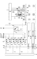
図1は本実施例の撮像装置の等価回路図である。光電変換ユニット100は、複数の光電変換素子を有し、ここでは第1光電変換素子101Aおよび第2光電変換素子101Bを有する。光電変換素子としてはフォトダイオードを用いることができる。
Example 1
FIG. 1 is an equivalent circuit diagram of the image pickup apparatus of the present embodiment. The
転送トランジスタ102A、102Bは複数の光電変換素子の各々に対応して設けられ、対応する光電変換素子の信号を増幅部の入力ノード103に転送する。複数の光電変換ユニットの各々に対応して配された複数のレンズを有するレンズアレイ(不図示)が光電変換素子の上部に配される。レンズアレイの各レンズは同一光電変換ユニットの複数の光電変換素子に集光する。各光電変換ユニットに含まれる複数の光電変換素子は平面視において、異なる位置に配される。
The
増幅部104は入力ノード103に転送された信号を増幅して共通出力線107へ出力する。増幅部104にはMOSトランジスタを用いることができる。
The amplifying
リセットトランジスタ105は増幅部の入力ノード103にリセット電圧を供給する。選択トランジスタ106は増幅部104と共通出力線107との間の電気的導通を制御する。
The
共通出力線107には電流源108が電気的に接続される。電流源108は増幅部104にバイアス電流を供給し、増幅部104と電流源108とでソースフォロアを構成する。
A
転送トランジスタ102A、102B、リセットトランジスタ105、選択トランジスタ106のゲートには、それぞれ駆動線109A、109B、駆動線110、駆動線111が接続される。それぞれのゲートには垂直走査回路112からの駆動パルスが、行ごとに順次もしくはランダムに供給される。
列回路は共通出力線107からの信号を受ける。列回路は共通出力線に直接もしくはスイッチを介して接続される。列回路で処理された信号は水平走査回路114により順次出力アンプ115に出力され外部へ出力される。
The column circuit receives a signal from the
列回路の主たる動作は共通出力線107の信号を入力容量116の容量値及びフィードバック容量117の容量値とで決まるゲインで反転増幅する。更には仮想接地動作も可能であり、入力容量116を用いたクランプ動作によりCDS(相関2重サンプリング)動作を行なうことが可能である。
The main operation of the column circuit is to invert and amplify the signal of the
次に、列回路の具体的な回路の一例を説明する。入力容量116は第1ノードが共通出力線107に電気的に接続され、第2ノードが演算増幅器119の反転入力ノードに電気的に接続される。フィードバック容量117の第1ノードは、演算増幅器119の反転入力ノード及び入力容量の第2ノードに電気的に接続される。フィードバック容量117の第2ノードは演算増幅器119の出力ノードに電気的に接続される。
Next, an example of a specific circuit of the column circuit will be described. The
スイッチ118は演算増幅器119の反転入力ノードと出力ノードとの間のフィードバック経路に、両者の電気的接続を制御するために設けられる。フィードバック容量117とスイッチ118とは並列に設けられる。
The
電源120は基準電圧Vrefを演算増幅器119の非反転入力ノードに供給する。保持容量121〜124は演算増幅器119からの出力を保持する容量である。スイッチ125〜128は保持容量121〜124と演算増幅器119との間の電気経路に設けられ、演算増幅器119の出力ノードと、保持容量121〜124との電気的導通を制御する。スイッチ129〜132は水平走査回路114からの信号を受けて、保持容量121〜124で保持された信号を水平出力線139、140へ出力させる。出力アンプ115は水平出力線139、140に出力された信号の差分を取り外部へ出力する。
The
駆動パルスPC0Rはスイッチ118へ供給される。駆動パルスPTNはスイッチ126、128へ供給される。駆動パルスPTSAはスイッチ125へ供給される。駆動パルスPTSABはスイッチ127へ供給される。
The drive pulse PC0R is supplied to the
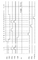
次に図1の撮像装置の駆動に関して図2を用いて説明する。いずれの駆動パルスもハイレベルのパルスで素子が導通状態になる。 Next, driving of the imaging apparatus of FIG. 1 will be described with reference to FIG. Any of the drive pulses is a high level pulse, and the element becomes conductive.
まず時刻T=t1において、駆動線109Aおよび109Bに供給される駆動パルスPTXAおよびPTXBがハイレベルとなる。この時、駆動線110に供給される駆動パルスPRESがハイレベルであるため、光電変換素子101A,101Bがリセットされる。
First, at time T = t1, the drive pulses PTXA and PTXB supplied to the
次にT=t2において、駆動パルスPTXAおよびPTXBがローレベルとなる。このタイミングで光電変換素子101A,101Bでの電荷蓄積期間が開始する。駆動パルスPRESはハイレベルを維持しているため、増幅部104の入力ノード103のリセット動作は継続している。
Next, at T = t2, the drive pulses PTXA and PTXB become low level. At this timing, the charge accumulation period in the
所定期間蓄積を行った後に各行ごと、もしくは複数行ごとに順次共通出力線107への信号の読み出しを行う。
After accumulation for a predetermined period, signals are sequentially read out to the
時刻T=t3において、選択トランジスタ106の駆動線111に供給される駆動パルスPSELがハイレベルとなり、選択トランジスタ106が導通する。これにより増幅部104の入力ノードの電位に応じた信号が共通出力線107に出力される。
At time T = t3, the drive pulse PSEL supplied to the
時刻T=t4でリセットトランジスタ105の駆動線110に供給される駆動パルスPRESをローレベルとすることにより増幅部104の入力ノード103のリセット動作を解除する。そしてリセット信号レベルを共通出力線107へ読み出し、列回路に入力する。この時、列回路は演算増幅器119が仮想接地状態となっている。具体的には駆動パルスPC0Rがハイレベルとなりスイッチ118が導通状態である。演算増幅器119はVrefの出力をバッファする状態でありこの状態で入力容量116にリセット信号レベルが供給される。
At time T = t4, the drive pulse PRES supplied to the
次にT=t5において駆動パルスPC0Rをローレベルとし、T=t6において駆動パルスPTNをローレベルからハイレベルへ切り替え、スイッチ126,128を導通状態とする。T=t7で駆動パルスPTNをハイレベルからローレベルへと切り替え、スイッチ126,128を非導通状態とする。この動作により略Vrefの出力が保持容量122,124へ供給され、その後保持容量122、124と演算増幅器119の出力ノードとが非導通となる。
Next, at T = t5, the drive pulse PC0R is set to the low level, and at T = t6, the drive pulse PTN is switched from the low level to the high level, and the
引き続きT=t8において、駆動パルスPTXAをハイレベルとし光電変換素子101Aの光電荷を増幅部104の入力ノード103へ転送し、T=t9において駆動パルスPTXAをローレベルとする。この動作により光電変換素子101Aの光電荷が入力ノード103へ転送される。これにより光電荷に基づく信号が増幅部104、共通出力線107を介して列回路へ供給される。この動作により、共通出力線に焦点検出用の信号を生じさせることができる。
Subsequently, at T = t8, the drive pulse PTXA is set to the high level, the photoelectric charge of the
列回路では入力容量116の容量値C0、フィードバック容量117の容量値Cfの比率で電圧変化に反転ゲインが掛け合された値が出力される。具体的には共通出力線107の電圧変化をΔVa(負)、演算増幅器119の出力をV(A)とすると、
V(A)=Vref+ΔVa×(−C0/Cf) 式(1)
となる。
The column circuit outputs a value obtained by multiplying the voltage change by the inversion gain at the ratio of the capacitance value C0 of the
V (A) = Vref + ΔVa × (−C0 / Cf) Equation (1)
It becomes.
次にT=t10において、駆動パルスPTSAをローレベルからハイレベルへ切り替えスイッチ125を導通させる。T=t11において駆動パルスPTSAをハイレベルからローレベルへと切り替え、スイッチ125を非導通とする。この動作により保持容量121に信号を保持する。
Next, at T = t10, the drive pulse PTSA is switched from the low level to the high level, and the
ひきつづきT=t12において、駆動パルスPTXAをハイレベルとし駆動パルスPTXAのハイレベル期間の少なくとも一部の期間で駆動パルスPTXBをハイレベルとする。この動作により光電変換素子101Aと101Bの双方の光電荷を同時に入力ノード103へ転送することができる。この動作により、共通出力線に画像形成用の信号を生じさせることができる。光電変換素子102Aの信号を転送してから、光電変換素子101Aと101Bの双方の光電荷を同時に入力ノード103へ転送するまでの間に増幅部104の入力ノード103はリセットされない。
Subsequently, at T = t12, the drive pulse PTXA is set to the high level, and the drive pulse PTXB is set to the high level during at least a part of the high level period of the drive pulse PTXA. With this operation, the photoelectric charges of both the
増幅部104の入力ノード103へ転送された電荷は光電変換素子101Aの電荷のみを転送した際と同様に列回路へ供給される。共通出力線107の電位変化をΔVa+b(負)、演算増幅器119の出力電位をV(A+B)とすると
V(A+B)=Vref+ΔVa+b×(−C0/Cf) 式(2)
となる。
The charge transferred to the
It becomes.
T=t14において、駆動パルスPTSABをローレベルからハイレベルへ切り替え、スイッチ122を導通させる。そしてT=t15において駆動パルスPTSABをハイレベルからローレベルへと切り替え、スイッチ122を非導通とする。この動作により演算増幅器119の出力ノードの電位V(A+B)を保持容量123へ書き込むことができる。
At T = t14, the drive pulse PTSAB is switched from the low level to the high level, and the
そして容量CTSABとCTNの差電圧である、
V(A+B)−Vref=ΔVa+b×(−C0/Cf) 式(3)
を得ることができる。これは光電変換ユニットに含まれる2つの光電変換素子の信号を加算して得られたものに相当する。光電変換ユニットに含まれる複数の光電変換素子で撮像をする際の1画素に相当する信号が得られる。
And the difference voltage between the capacitors CTSAB and CTN.
V (A + B) −Vref = ΔVa + b × (−C0 / Cf) Equation (3)
Can be obtained. This corresponds to a signal obtained by adding signals of two photoelectric conversion elements included in the photoelectric conversion unit. A signal corresponding to one pixel when imaging with a plurality of photoelectric conversion elements included in the photoelectric conversion unit is obtained.
また、保持容量121と122の電位差
V(A)−Vref=ΔVa×(−C0/Cf) 式(4)
を得ることで、光電変換素子101Aのみの信号を得ることができる。光電変換素子101Aによって得られる信号は集光された撮影レンズの瞳の一部を透過する光束の情報に相当する。さらにこれらの電位差すなわち
(ΔVa+b×(−C0/Cf))−(ΔVa×(−C0/Cf))
=(ΔVa+b−ΔVa)×(−C0/Cf) 式(5)
を得ることにより光電変換素子101Bのみの信号を得ることができる。光電変換素子101Bよって得られる信号は集光された撮影レンズの瞳の一部を透過する光束の情報が得られる。各光電変換ユニットに含まれる複数の光電変換素子は平面視において、異なる位置に配される。そして光電変換素子101A、101Bの2つの光束の情報から焦点検出を行なうことができる。
Further, the potential difference V (A) −Vref = ΔVa × (−C0 / Cf) between the
As a result, a signal of only the
= (ΔVa + b−ΔVa) × (−C0 / Cf) Equation (5)
As a result, a signal of only the
上記演算は撮像装置内で行うこともできるし、撮像装置から出力された後に信号処理部で行うこともできる。ただし光電変換素子101Aのみの信号、及び光電変換素子101A、101Bの加算後の信号は撮像装置内で得られる。
The calculation can be performed in the imaging apparatus, or can be performed in the signal processing unit after being output from the imaging apparatus. However, the signal of only the
次にT=t16で駆動パルスPRESをハイレベルとし、リセット部105を導通させ、入力ノード103の電位をリセットする。
Next, at T = t16, the drive pulse PRES is set to the high level, the
保持容量121〜124に保持された信号はT=t17以降にパルスPHに同期した駆動パルス133、134が順次導通することで読み出される。本実施例によれば水平出力線139、140の後段に差分処理を行なうことが可能な出力アンプ115を有しているため、保持容量121,122に保持された信号の差分を撮像装置外部に出力することができる。更に保持容量123,124に保持された信号の差分を撮像装置外部に出力することができる。これにより水平出力線139,140において生じるノイズを低減することができる。しかしながら出力アンプ115は必ずしも差分出力を得る構成である必要はなく単なるバッファ段でもよい。これ以降、順次各列の信号が水平走査回路114により走査されて水平出力線139,140に読み出される。
The signals held in the holding
なお、読み出しの順番は光電変換素子Aのみの信号を読み出した後に光電変換素子AおよびBの加算信号を読み出す例を示したが、順番を入れ替えてもよい。光電変換素子Aのみの信号を先に読み出すことで、よりよい信号が得られる。なぜならば保持容量121〜124に保持されている時間が長いほど容量およびスイッチによるリーク電流の影響を受けやすくなるからである。
In addition, although the example of reading the addition signal of the photoelectric conversion elements A and B after reading the signal of only the photoelectric conversion element A is shown as the order of reading, the order may be changed. By reading the signal of only the photoelectric conversion element A first, a better signal can be obtained. This is because the longer the time held in the holding
本実施例の特徴は期間t11〜t15の動作にある。 The feature of this embodiment is the operation during the period t11 to t15.
特許文献1には、以下の動作が開示されている。第1の光電変換素子の信号を保持容量に書き込み、水平転送動作を行い、信号を撮像装置外へ読み出す。そしてリセットトランジスタによりリセット動作を行なう。その後、第2の光電変換素子の信号を保持容量に書き込み、水平転送動作を行い、信号をセンサ外へ読み出す。そして再度リセットトランジスタによりリセット動作を行なう。
この場合、第1光電変換素子の信号と第2光電変換素子の信号とを読み出す間には1行分の読み出し時間差(数十〜数百μsec)が発生してしまう。 In this case, a reading time difference (several tens to several hundreds μsec) for one row occurs between reading the signal of the first photoelectric conversion element and the signal of the second photoelectric conversion element.
本実施例では光電変換素子101Aの信号を読み終え、T=t11で保持容量に信号を書き込む。入力ノード103に光電変換素子101Aの信号を保持したまま、T=t12において光電変換素子101A、101Bの双方の信号を読み出す。このことにより読み出し時間は大幅(数μsec)に短縮される。更に、光電変換素子101A、101B間の信号読み出しの時間差が短くなり、焦点検出の精度を高くする効果がある。
In this embodiment, the signal of the
また本実施例の副次的な特徴は時刻T=t8〜t15の動作にある。駆動パルスPTXA、PTXBを同時にハイレベルにすることにより以下の効果が得られる。 A secondary feature of this embodiment is the operation from time T = t8 to t15. The following effects can be obtained by simultaneously setting the drive pulses PTXA and PTXB to the high level.
まず1点目として、一般に、転送トランジスタのゲート電位がローレベルからハイレベルに遷移する際に転送トランジスタの駆動配線と、入力ノードとの容量結合により入力ノード103の電位が上昇する。本実施例では2つの転送トランジスタ102A,102Bのゲート電位がローレベルからハイレベルに遷移する。したがって1つの転送トランジスタの場合より入力ノード103の電位の上昇分が大きくなる。入力ノード103の電位が高くなると光電変換素子101A,101Bの電荷が入力ノード103に転送されやすくなる。したがって転送効率が向上する。
First, as a first point, generally, when the gate potential of the transfer transistor transitions from a low level to a high level, the potential of the
特に本実施例の撮像装置のように、1つの撮像用の画素を2つの光電変換素子に分けて構成している場合、光電変換素子101Aと101Bの間にはポテンシャル障壁を設ける場合が多い。このポテンシャル障壁により、光電変換素子のポテンシャル分布が複雑になる。このため転送時の電荷残りが発生しやすく固定パタンノイズ、ランダムノイズが生じる場合がある。これに対して駆動パルスPTXA、PTXBを同時刻にハイレベルとすることにより入力ノードの電位を高い状態で固定パタンノイズ、ランダムノイズを低減する効果がある。
In particular, when one imaging pixel is divided into two photoelectric conversion elements as in the imaging apparatus of this embodiment, a potential barrier is often provided between the
2点目として、光電変換素子101A、101Bの蓄積時間の差を小さくすることができる。たとえば特許文献1の構成では2つの光電変換素子における蓄積時間がずれてしまう。これに対し、本実施形態のように、入力ノード103で加算する際に、加算を行なう光電変換素子に対応するすべての転送ゲートをオフするタイミングを略同一にすることで蓄積時間を揃えることができる。これは撮像装置の撮像面において焦点検出用の信号を得る構成において特に有効である。
As a second point, the difference in accumulation time between the
本実施例においては焦点検出用の信号を生じさせるために1つの光電変換素子の信号を用いたが、1光電変換ユニットに更に多数の光電変換素子が含まれる場合にはこれに限られるものではない。ただし、焦点検出用の信号を得るためには1光電変換ユニットに含まれる全ての光電変換素子の信号を用いることはできない。これは以下の実施例においても同様である。 In this embodiment, the signal of one photoelectric conversion element is used to generate a focus detection signal, but this is not limited to the case where a larger number of photoelectric conversion elements are included in one photoelectric conversion unit. Absent. However, in order to obtain a focus detection signal, signals of all photoelectric conversion elements included in one photoelectric conversion unit cannot be used. The same applies to the following embodiments.
また第2の動作において1光電変換ユニットに含まれる全ての光電変換素子(ここでは二つ)の信号を読出したがこれに限られるものではない。少なくとも第1の動作で読み出しが行われなかった光電変換素子の信号を読み出せばよい。これも以下の実施例においても同様である。 In the second operation, the signals of all the photoelectric conversion elements (here, two) included in one photoelectric conversion unit are read out, but the present invention is not limited to this. At least the signal of the photoelectric conversion element which has not been read out in the first operation may be read out. This also applies to the following embodiments.
(実施例2)
図3に第2の実施例の撮像装置の等価回路図を示す。
(Example 2)
FIG. 3 shows an equivalent circuit diagram of the image pickup apparatus of the second embodiment.
実施例1との差異は、光電変換ユニットおよび列回路の構成である。1つの光電変換ユニットに含まれる光電変換素子の数が3つとなりこれに応じて、列回路に含まれる保持容量の数も6つとなっている。実施例1と同様の機能を有する部分には同様の符号を付し詳細な説明は省略する。 The difference from the first embodiment is the configuration of the photoelectric conversion unit and the column circuit. The number of photoelectric conversion elements included in one photoelectric conversion unit is three, and accordingly, the number of storage capacitors included in the column circuit is also six. Parts having the same functions as those in the first embodiment are denoted by the same reference numerals, and detailed description thereof is omitted.
光電変換ユニット200は光電変換素子101A〜101Cを有する。実施例1に比べて撮像用の1画素に含まれる光電変換素子の分割数を増やしているため更に高い精度の焦点検出が可能となる。
The
光電変換素子101A〜101Cの電荷を転送する転送トランジスタ102A〜102Cを有する。転送トランジスタ102Cの駆動パルスとしてPTXCが追加される。
列回路210は、光電変換素子101A〜101Cの加算後の信号を保持するための保持容量201を新たに有している。またノイズレベルを保持するための保持容量202も新たに追加される。これらに対応してスイッチ203〜206が追加される。
The
次に図4を用いて本実施例の撮像装置の駆動方法を説明する。基本的な動作は図2と同様であるため実施例1と異なる部分を中心に説明を行なう。 Next, the driving method of the image pickup apparatus of the present embodiment will be described with reference to FIG. Since the basic operation is the same as that in FIG. 2, the description will focus on the differences from the first embodiment.
時刻T=t12において駆動パルスPTXAとPTXBの双方がハイレベルとなる。この動作により光電変換素子101A、101Bの信号が入力ノード103で加算される。ここでは駆動パルスPTXA、PTXBの両者をハイレベルとしているが、駆動パルスPTXBのみをハイレベルとしてもよい。そして時刻T=t16において、駆動パルスPTXA,PTXB,PTXCの全てをハイレベルとする。この動作により光電変換素子101A〜101Cの電荷が入力ノード103で加算される。時刻T=t17において駆動パルスPTXA,PTXB,PTXCの全てをローレベルとする。このような動作により光電変換素子101A〜101Cの蓄積時間を期間t2〜t17の期間に揃えることが可能となる。
At time T = t12, both the drive pulses PTXA and PTXB are at a high level. By this operation, the signals of the
先に光電変換素子101A〜101Cの加算信号を読み出した後に光電変換素子101Aのみの信号、光電変換素子101A、101Bの加算信号を読み出してもよい。
It is also possible to read out only the signals from the
光電変換素子101Aのみの信号、光電変換素子101A、101Bの加算信号、光電変換素子101A〜101Cの加算信号をこの順で読み出すことで、よりよい信号が得られる。なぜならば保持容量121〜124、201,202に保持されている時間が長いほど容量およびスイッチによるリーク電流の影響を受けやすくなるからである。
A better signal can be obtained by reading out the signal of only the
(実施例3)
図5に第3の実施例の撮像装置の等価回路図を示す。実施例1、2との差異は、互いに異なる光電変換ユニットに含まれる複数の光電変換素子で増幅部104を共有する点である。
(Example 3)
FIG. 5 shows an equivalent circuit diagram of the image pickup apparatus of the third embodiment. The difference from the first and second embodiments is that the amplifying
図5では、光電変換素子501A,501Bを有する第1光電変換ユニットと、光電変換素子502A,502Bとを有する第2光電変換ユニットとを有する。第1光電変換ユニットに含まれる複数の光電変換素子には第1マクロレンズにより集光された光が入射し、第2光電変換ユニットに含まれる複数の光電変換素子には第2マイクロレンズにより集光された光が入射する。
5 includes a first photoelectric conversion unit having
それぞれの光電変換素子501A、501B、502A、502Bに対応して、転送トランジスタ503A,503B、504A,504Bを有している。転送トランジスタ503A、503B、504A、504Bに駆動パルスを供給する配線として、駆動線505A、505B、506A、506Bが配されている。
このような構成によれば増幅部104、リセット部105、選択部106を撮像用の複数の画素で共有化することができる。これにより撮像用の1画素あたりのトランジスタ数を削減することが可能となる。その結果、光電変換素子の面積を拡大させることができる。
According to such a configuration, the
それぞれの光電変換素子501A,501B、502A,502Bを順次読みだす際の動作に関しては図2と基本的に同様な読み出しをおこなうことで、異なる行の信号として読み出すことができる。具体的には、第1光電変換ユニットでは光電変換素子501Aの信号を読み出したのちに、光電変換素子501A、501Bの信号を入力ノード103で加算する。これにより焦点検出量の信号と撮像用の信号の両者を生じさせることができる。続いて第2光電変換ユニットでは光電変換素子502Aの信号を読み出したのちに、光電変換素子502A、502Bの信号を入力ノード103で加算する。これにより焦点検出量の信号と撮像用の信号の両者を生じさせることができる。
With respect to the operation when sequentially reading out each of the
更に本実施例では異なる2つの光電変換ユニットで増幅部104を共有している。したがって光電変換素子501A、502Aの信号を入力ノード103で加算し、光電変換素子501B、502Bの信号を入力ノード103で加算することもできる。具体的な駆動タイミングの一例を図6に示す。本実施例に特徴的な部分を中心に説明する。ここで転送トランジスタ503Aに供給される駆動パルスをPTXA(505A)、転送トランジスタ503Bに供給される駆動パルスをPTXB(505B)とする。更に、転送トランジスタ504Aに供給される駆動パルスをPTXA(506A)、転送トランジスタ504Bに供給される駆動パルスをPTXB(506B)とする。
Furthermore, in this embodiment, the
時刻T=t8において、駆動パルスPTXA(505A)、PTXA(506A)をローレベルからハイレベルとする。その後時刻T=t9において、駆動パルスPTXA(505A)、PTXA(506A)をハイレベルからローレベルとする。この動作により異なる光電変換ユニットに含まれる光電変換素子501A、502Aの信号が入力ノード103で加算される。この信号は焦点検出用の信号として用いられる。
At time T = t8, the drive pulses PTXA (505A) and PTXA (506A) are changed from the low level to the high level. Thereafter, at time T = t9, the drive pulses PTXA (505A) and PTXA (506A) are changed from the high level to the low level. By this operation, signals of the
そして時刻T=t12において、駆動パルスPTXA(505A)、PTXB(505B)PTXA(506A)、PTXB(506B)をローレベルからハイレベルとする。その後、T=t13において、駆動パルスPTXA(505A)、PTXB(505B)PTXA(506A)、PTXB(506B)をローレベルからハイレベルとする。この動作により異なる光電変換ユニットに含まれる全ての光電変換素子501A、501B、502A、502Bの信号が入力ノード103で加算される。この信号は撮像用の信号として用いられる。
At time T = t12, the drive pulses PTXA (505A), PTXB (505B), PTXA (506A), and PTXB (506B) are changed from the low level to the high level. Thereafter, at T = t13, the drive pulses PTXA (505A), PTXB (505B), PTXA (506A), and PTXB (506B) are changed from the low level to the high level. By this operation, the signals of all the
本動作により焦点検出用の信号が、異なる光電変換ユニットに含まれる複数の光電変換素子の信号を加算して得ているためS/Nが向上する。このためより精度の高い焦点検出が可能となる。 This operation improves the S / N because the focus detection signal is obtained by adding the signals of a plurality of photoelectric conversion elements included in different photoelectric conversion units. This makes it possible to detect the focus with higher accuracy.
なお、本実施例では2つの撮像用の画素の信号を加算する例を示したがこれが3つ以上であっても同様の効果が得られる。 In the present embodiment, an example in which signals of two imaging pixels are added has been described, but the same effect can be obtained even if there are three or more.
(実施例4)
図7は第4の実施例の撮像装置の等価回路図である。本実施例の実施例3と異なる点は、複数の入力ノード103を電気的に接続するためのスイッチを設けた点である。実施例1〜3の構成と同様の機能を有する部分には同様の符号を付し詳細な説明は省略する。
Example 4
FIG. 7 is an equivalent circuit diagram of the image pickup apparatus according to the fourth embodiment. The difference of the present embodiment from the third embodiment is that a switch for electrically connecting a plurality of
図7において第1光電変換ユニットは光電変換素子701A、701Bを有している。第2光電変換ユニットは光電変換素子702A、702Bを有している。第3光電変換ユニットは光電変換素子721A、721Bを有している。第4光電変換ユニットは光電変換素子722A、722Bを有している。第1及び第2光電変換ユニットに対し、共有化された増幅部707が配されている。第3及び第4光電変換ユニットに対し、共有化された増幅部727が配されている。
In FIG. 7, the first photoelectric conversion unit includes
それぞれの光電変換素子に対応して転送トランジスタ703A、703B、704A、704B、723A、723B、724A、724Bが配されている。そしてそれぞれの転送トランジスタを駆動するための駆動配線705A、705B、706A、706B、725A、725B、726A、726Bが配されている。
スイッチ740は増幅部707,727の入力ノードを電気的に接続する。スイッチ740は駆動配線741により制御される。
The
図8に図7の駆動パルス図を示す。ここでは第1光電変換ユニット及び第3光電変換ユニットに対応する部分のみ抜き出して説明する。第2、第4光電変換ユニットも同様の駆動を行なうことができる。駆動パルスPTXA(705A)は駆動配線705Aに供給されるパルスである。駆動パルスPTXB(705B)は駆動配線705Bに供給されるパルスである。駆動パルスPTXA(725A)は駆動配線725Aに供給されるパルスである。駆動パルスPTXB(725B)は駆動配線725Bに供給されるパルスである。PVADD(741)は駆動配線741に供給されるパルスである。
FIG. 8 shows a drive pulse diagram of FIG. Here, only portions corresponding to the first photoelectric conversion unit and the third photoelectric conversion unit are extracted and described. The second and fourth photoelectric conversion units can be driven in the same manner. The drive pulse PTXA (705A) is a pulse supplied to the
図8においては第1光電変換ユニット、第3光電変換ユニットに含まれる光電変換素子701A、721Aの信号を加算する例を示す。
FIG. 8 shows an example in which signals from the
PVADD(741)は図8に図示されている期間においてはハイレベルが維持されている。つまり増幅部707,727の入力ノードが常に電気的に接続された状態である。
PVADD (741) is maintained at a high level during the period shown in FIG. That is, the input nodes of the amplifying
T=t8において、駆動パルスPTXA(705A)、PTXA(725A)をローレベルからハイレベルとする。その後、時刻T=t9において、駆動パルスPTXA(705A)、PTXA(725A)をハイレベルからローレベルとする。この動作により異なる光電変換ユニットに含まれる光電変換素子701A、721Aの信号が各々対応する増幅部707,727へ転送される。そしてスイッチ740は導通状態となっているため、両信号は加算される。この信号は焦点検出用の信号として用いられる。
At T = t8, the drive pulses PTXA (705A) and PTXA (725A) are changed from the low level to the high level. Thereafter, at time T = t9, the drive pulses PTXA (705A) and PTXA (725A) are changed from the high level to the low level. By this operation, signals from the
そして時刻T=t12において、駆動パルスPTXA(705A)、PTXB(705B)、PTXA(725A)、PTXB(725B)をローレベルからハイレベルとする。その後、T=t13において、駆動パルスPTXA(705A)、PTXB(705B)PTXA(725A)、PTXB(725B)をローレベルからハイレベルとする。この動作により異なる光電変換ユニットに含まれる複数の光電変換素子701A、701B、721A、721Bの信号が対応する増幅部707,727へ転送される。そしてスイッチ740は導通状態となっているため、全ての信号は加算される。この信号は撮像用の信号として用いられる。
At time T = t12, the drive pulses PTXA (705A), PTXB (705B), PTXA (725A), and PTXB (725B) are changed from the low level to the high level. Thereafter, at T = t13, the drive pulses PTXA (705A), PTXB (705B), PTXA (725A), and PTXB (725B) are changed from the low level to the high level. By this operation, the signals of the plurality of
本実施例においては複数の入力ノードを電気的に接続する機能が付加された。これにより、カラーフィルタを有する撮像装置において、同色の信号が離間して配されている場合、例えば、ベイヤ配列のカラーフィルタを有する場合に適している。離間して配されている同色の光電変換素子の信号を加算することが可能となるためである。そのため、焦点検出だけでなく画像信号のS/Nも向上し精度の高い焦点検出と同時に高画質な画像情報を得ることができる。 In the present embodiment, a function of electrically connecting a plurality of input nodes is added. Thereby, in an imaging device having a color filter, it is suitable when signals of the same color are arranged apart from each other, for example, when a color filter having a Bayer array is provided. This is because it is possible to add signals of photoelectric conversion elements of the same color that are spaced apart. Therefore, not only the focus detection but also the S / N of the image signal can be improved, and high-quality image information can be obtained simultaneously with high-precision focus detection.
なお、本実施例では2つの入力ノードを接続する例を示したが、3つ以上に関しても同様の効果が得られる。 In addition, although the example which connects two input nodes was shown in the present Example, the same effect is acquired also about three or more.
以上具体的な実施例を挙げて本発明の説明を行ったが、本発明は上記実施の形態に制限されるものではなく、本発明の精神及び範囲から離脱することなく、様々な変更及び変形が可能である。例えば画素の回路構成はこれに限るものではなく、選択部を有さずにリセット部により入力ノードの電位を切り替えることにより選択、非選択を切り替える構成であってもよい。更に列回路として演算増幅器を有する構成としたがソース接地増幅回路のようなより簡易な構成とすることもできる。もしくはゲイン段を複数設ける、ゲイン段とバッファ段との組み合わせにするなど各種変形が可能である。また共通出力線を画素列に対して1本設けたが、1画素列に対し複数の共通出力線を設けてもよい。 Although the present invention has been described with reference to specific examples, the present invention is not limited to the above embodiments, and various changes and modifications can be made without departing from the spirit and scope of the present invention. Is possible. For example, the circuit configuration of the pixel is not limited to this, and may be configured to switch between selection and non-selection by switching the potential of the input node by the reset unit without having the selection unit. Furthermore, although the operational amplifier is provided as the column circuit, a simpler construction such as a common-source amplifier circuit may be employed. Alternatively, various modifications such as providing a plurality of gain stages or combining a gain stage and a buffer stage are possible. One common output line is provided for each pixel column, but a plurality of common output lines may be provided for one pixel column.
100、200、300、700、720 光電変換ユニット
101A、101B、501A,B、502A,B、701A,B、702A,B、721A,B、722A,B 光電変換素子
104、707、727 増幅部
105、708、728 リセット部
107 共通出力線
100, 200, 300, 700, 720
Claims (15)
前記光電変換ユニットの複数の光電変換素子のうち少なくとも1つの光電変換素子の信号を前記増幅部の入力ノードへ読み出し、前記増幅部を介して前記共通出力線へ信号を読み出す第1の動作により焦点検出用の信号を生じさせ、
前記第1の動作により読み出された信号が前記増幅部において保持された状態で、同じ光電変換ユニットに含まれる、少なくとも前記第1の動作で読み出しを行なわれていない光電変換素子の信号を前記増幅部の入力ノードへ読み出して、前記増幅部を介して前記共通出力線へ信号を読み出す第2の動作により画像形成用の信号を生じさせ、
前記複数の列回路において保持された、所定行の複数の前記光電変換ユニットで生じた前記焦点検出用の信号と前記画像形成用の信号とを、まとめて水平出力線へ出力することを特徴とする撮像装置の駆動方法。 A plurality of photoelectric conversion units each having a plurality of photoelectric conversion elements; a plurality of amplifying units each amplifying signals of the plurality of photoelectric conversion elements shared by the plurality of photoelectric conversion elements of the photoelectric conversion unit; A plurality of common output lines from which signals from the amplification unit are output, a plurality of column circuits receiving signals from any of the plurality of common output lines, and signals processed by the plurality of column circuits are output. A driving method of an imaging device having a horizontal output line,
A focus is obtained by a first operation of reading a signal of at least one of the plurality of photoelectric conversion elements of the photoelectric conversion unit to an input node of the amplification unit and reading a signal to the common output line through the amplification unit. A signal for detection,
In a state where the signal read out by the first operation is held in the amplifying unit, the signal of the photoelectric conversion element that is included in the same photoelectric conversion unit and has not been read out at least in the first operation A signal for image formation is generated by the second operation of reading to the input node of the amplifying unit and reading the signal to the common output line via the amplifying unit,
The focus detection signals and the image formation signals generated in the plurality of photoelectric conversion units in a predetermined row and held in the plurality of column circuits are collectively output to a horizontal output line. Method of driving an imaging apparatus.
前記光電変換ユニットの複数の光電変換素子のうち少なくとも1つの光電変換素子の信号を前記増幅部の入力ノードへ読み出し、前記増幅部を介して前記共通出力線へ信号を読み出す第1の動作と、
前記第1の動作により読み出された信号が前記増幅部において保持された状態で、同じ光電変換ユニットに含まれる、少なくとも前記第1の動作で読み出しを行なわれていない光電変換素子の信号を前記増幅部の入力ノードへ読み出して、前記増幅部を介して前記共通出力線へ信号を読み出す第2の動作とを有し、
前記複数の列回路において保持された、所定行の複数の前記光電変換ユニットで生じた前記第1の動作で読み出された信号と前記第2の動作で読み出された信号とを、まとめて水平出力線へ出力することを特徴とする撮像装置の駆動方法。 A plurality of photoelectric conversion units each having a plurality of photoelectric conversion elements; a plurality of amplifying units each amplifying signals of the plurality of photoelectric conversion elements shared by the plurality of photoelectric conversion elements of the photoelectric conversion unit; A plurality of common output lines from which signals from the amplification unit are output, a plurality of column circuits receiving signals from any of the plurality of common output lines, and signals processed by the plurality of column circuits are output. A plurality of photoelectric conversion elements, each of which is a driving method of an imaging device that receives light from different areas of the pupil of a photographing lens,
A first operation of reading a signal of at least one photoelectric conversion element among a plurality of photoelectric conversion elements of the photoelectric conversion unit to an input node of the amplification unit, and reading a signal to the common output line via the amplification unit;
In a state where the signal read out by the first operation is held in the amplifying unit, the signal of the photoelectric conversion element that is included in the same photoelectric conversion unit and has not been read out at least in the first operation A second operation of reading to the input node of the amplifying unit and reading a signal to the common output line via the amplifying unit;
The signals read in the first operation and the signals read in the second operation generated in the plurality of photoelectric conversion units in a predetermined row held in the plurality of column circuits are collectively A method for driving an imaging apparatus, characterized by outputting to a horizontal output line.
前記光電変換ユニットの複数の光電変換素子のうち少なくとも1つの光電変換素子の信号を前記増幅部の入力ノードへ読み出し、前記増幅部を介して前記共通出力線へ信号を読み出す第1の動作と、
前記第1の動作により読み出された信号が前記増幅部において保持された状態で、同じ光電変換ユニットに含まれる、少なくとも前記第1の動作で読み出しを行なわれていない光電変換素子の信号を前記増幅部の入力ノードへ読み出して、前記増幅部を介して前記共通出力線へ信号を読み出す第2の動作とを有し、
前記複数の列回路において保持された、所定行の複数の前記光電変換ユニットで生じた前記第1の動作で読み出された信号と前記第2の動作で読みだされた信号とを、まとめて水平出力線へ出力することを特徴とする撮像装置の駆動方法。 A plurality of photoelectric conversion units each having a plurality of photoelectric conversion elements; a plurality of amplifying units each amplifying signals of the plurality of photoelectric conversion elements shared by the plurality of photoelectric conversion elements of the photoelectric conversion unit; A plurality of common output lines from which signals from the amplification unit are output, a plurality of column circuits receiving signals from any of the plurality of common output lines, and signals processed by the plurality of column circuits are output. A horizontal output line, and a lens array having a plurality of lenses arranged corresponding to each of the plurality of photoelectric conversion units, wherein each lens of the lens array has a plurality of photoelectric conversion units of the same photoelectric conversion unit. A method for driving an imaging device that focuses light on a conversion element,
A first operation of reading a signal of at least one photoelectric conversion element among a plurality of photoelectric conversion elements of the photoelectric conversion unit to an input node of the amplification unit, and reading a signal to the common output line via the amplification unit;
In a state where the signal read out by the first operation is held in the amplifying unit, the signal of the photoelectric conversion element that is included in the same photoelectric conversion unit and has not been read out at least in the first operation A second operation of reading to the input node of the amplifying unit and reading a signal to the common output line via the amplifying unit;
The signals read out in the first operation and the signals read out in the second operation, which are held in the plurality of column circuits and are generated in the plurality of photoelectric conversion units in a predetermined row, are collected together. A method for driving an imaging apparatus, characterized by outputting to a horizontal output line.
前記第2の動作時に前記第1の光電変換ユニットに含まれる複数の光電変換素子の信号と前記第2の光電変換ユニットに含まれる複数の光電変換素子の信号とを、前記共有された増幅部で加算することを特徴とする請求項6に記載の撮像装置の駆動方法。 During the first operation, signals of at least two photoelectric conversion elements included in each of the first and second photoelectric conversion units that share the amplification unit are added by the shared amplification unit,
In the second operation, the shared amplifying unit outputs signals from a plurality of photoelectric conversion elements included in the first photoelectric conversion unit and signals from a plurality of photoelectric conversion elements included in the second photoelectric conversion unit. The image pickup apparatus driving method according to claim 6, wherein the addition is performed in a step.
前記第2の動作時に前記スイッチを導通させることで、複数の前記増幅部の入力ノードを電気的に接続し、前記接続された入力ノードの信号を加算することを特徴とする請求項8に記載の撮像装置の駆動方法。 By electrically connecting the switch during the first operation, the input nodes of the plurality of amplification units are electrically connected, and the signals of the connected input nodes are added,
9. The switch according to claim 8, wherein the switch is turned on during the second operation to electrically connect the input nodes of the plurality of amplifying units and add signals of the connected input nodes. Driving method of the imaging apparatus.
前記第1の動作時に、前記転送ゲートが導通するパルスを供給することで、前記光電変換素子の信号を対応する前記増幅部の入力ノードへ転送し、
前記第2の動作時に、前記第1の動作時に信号が転送される光電変換素子に対応する転送ゲートが導通状態となる期間の少なくとも一部の期間において、前記第2の動作時に信号が転送される光電変換素子に対応する転送ゲートの両者が導通状態となることを特徴とする請求項1〜9のいずれか1項に記載の撮像装置の駆動方法。 A plurality of transfer gates for transferring each signal of a plurality of photoelectric conversion elements to a corresponding input node of the amplifying unit;
In the first operation, by supplying a pulse that makes the transfer gate conductive, the signal of the photoelectric conversion element is transferred to the corresponding input node of the amplification unit,
During the second operation, a signal is transferred during the second operation in at least a part of a period during which the transfer gate corresponding to the photoelectric conversion element to which the signal is transferred during the first operation is in a conductive state. The driving method of the imaging apparatus according to claim 1, wherein both of the transfer gates corresponding to the photoelectric conversion elements are in a conductive state.
前記光電変換ユニットの複数の光電変換素子のうち少なくとも1つの光電変換素子の信号を前記増幅部の入力ノードへ読み出し、前記増幅部を介して前記共通出力線へ信号を読み出す第1の動作により焦点検出用の信号を生じさせ、
前記第1の動作により読み出された信号が前記増幅部において保持された状態で、同じ光電変換ユニットに含まれる少なくとも前記第1の動作で読み出されなかった光電変換素子の信号を前記増幅部の入力ノードへ読み出して、前記増幅部を介して前記共通出力線へ信号を読み出す第2の動作により画像形成用の信号を生じさせ、
前記複数の列回路において保持された、所定行の複数の前記光電変換ユニットで生じた前記焦点検出用の信号と前記画像形成用の信号とを、まとめて水平出力線へ出力することを特徴とする撮像装置。 A plurality of photoelectric conversion units each having a plurality of photoelectric conversion elements; a plurality of amplifying units each amplifying signals of the plurality of photoelectric conversion elements shared by the plurality of photoelectric conversion elements of the photoelectric conversion unit; A plurality of common output lines from which signals of the amplification unit are output, a plurality of column circuits receiving signals from any of the plurality of common output lines, and signals processed by the plurality of column circuits are output. An imaging device having a horizontal output line,
A focus is obtained by a first operation of reading a signal of at least one of the plurality of photoelectric conversion elements of the photoelectric conversion unit to an input node of the amplification unit and reading a signal to the common output line through the amplification unit. A signal for detection,
In the state where the signal read out by the first operation is held in the amplification unit, at least the signal of the photoelectric conversion element included in the same photoelectric conversion unit and not read out in the first operation is sent to the amplification unit A signal for image formation is generated by a second operation of reading the signal to the input node and reading the signal to the common output line via the amplifier,
The focus detection signals and the image formation signals generated in the plurality of photoelectric conversion units in a predetermined row and held in the plurality of column circuits are collectively output to a horizontal output line. An imaging device.
前記複数の光電変換素子は、各々が、撮影レンズの瞳の異なる領域からの光を受光する撮像装置であって、
前記光電変換ユニットの複数の光電変換素子のうち少なくとも1つの光電変換素子の信号を前記増幅部の入力ノードへ読み出し、前記増幅部を介して前記共通出力線へ信号を読み出す第1の動作と、
前記第1の動作により読み出された信号が前記増幅部において保持された状態で、同じ光電変換ユニットに含まれる少なくとも前記第1の動作で読み出されなかった光電変換素子の信号を前記増幅部の入力ノードへ読み出して、前記増幅部を介して前記共通出力線へ信号を読み出す第2の動作とを行ない、
前記複数の列回路において保持された、所定行の複数の前記光電変換ユニットで生じた前記第1の動作で読み出された信号と前記第2の動作で読み出された信号とを、まとめて水平出力線へ出力することを特徴とする撮像装置。 A plurality of photoelectric conversion units each having a plurality of photoelectric conversion elements; a plurality of amplifying units each amplifying signals of the plurality of photoelectric conversion elements shared by the plurality of photoelectric conversion elements of the photoelectric conversion unit; A plurality of common output lines from which signals of the amplification unit are output, a plurality of column circuits receiving signals from any of the plurality of common output lines, and signals processed by the plurality of column circuits are output. A horizontal output line,
Each of the plurality of photoelectric conversion elements is an imaging device that receives light from different regions of a pupil of a photographing lens,
A first operation of reading a signal of at least one photoelectric conversion element among a plurality of photoelectric conversion elements of the photoelectric conversion unit to an input node of the amplification unit, and reading a signal to the common output line via the amplification unit;
In the state where the signal read out by the first operation is held in the amplification unit, at least the signal of the photoelectric conversion element included in the same photoelectric conversion unit and not read out in the first operation is sent to the amplification unit And a second operation of reading a signal to the common output line through the amplifier,
The signals read in the first operation and the signals read in the second operation generated in the plurality of photoelectric conversion units in a predetermined row held in the plurality of column circuits are collectively An image pickup apparatus that outputs to a horizontal output line.
前記光電変換ユニットの複数の光電変換素子のうち少なくとも1つの光電変換素子の信号を前記増幅部の入力ノードへ読み出し、前記増幅部を介して前記共通出力線へ信号を読み出す第1の動作と、
前記第1の動作により読み出された信号が前記増幅部において保持された状態で、同じ光電変換ユニットに含まれる少なくとも前記第1の動作で読み出されなかった光電変換素子の信号を前記増幅部の入力ノードへ読み出して、前記増幅部を介して前記共通出力線へ信号を読み出す第2の動作とを行い、
前記複数の列回路において保持された、所定行の複数の前記光電変換ユニットで生じた前記第1の動作で読み出された信号と前記第2の動作で読み出された信号とを、まとめて水平出力線へ出力することを特徴とする撮像装置。 A plurality of photoelectric conversion units each having a plurality of photoelectric conversion elements; a plurality of amplifying units each amplifying signals of the plurality of photoelectric conversion elements shared by the plurality of photoelectric conversion elements of the photoelectric conversion unit; A plurality of common output lines from which signals of the amplification unit are output, a plurality of column circuits receiving signals from any of the plurality of common output lines, and signals processed by the plurality of column circuits are output. And a lens array having a plurality of lenses arranged corresponding to each of the plurality of photoelectric conversion units, each lens of the lens array having a plurality of photoelectric conversions of the same photoelectric conversion unit An imaging device that focuses light on an element,
A first operation of reading a signal of at least one photoelectric conversion element among a plurality of photoelectric conversion elements of the photoelectric conversion unit to an input node of the amplification unit, and reading a signal to the common output line via the amplification unit;
In the state where the signal read out by the first operation is held in the amplification unit, at least the signal of the photoelectric conversion element included in the same photoelectric conversion unit and not read out in the first operation is sent to the amplification unit And a second operation of reading a signal to the common output line via the amplifier,
The signals read in the first operation and the signals read in the second operation generated in the plurality of photoelectric conversion units in a predetermined row held in the plurality of column circuits are collectively An image pickup apparatus that outputs to a horizontal output line.
Priority Applications (1)
| Application Number | Priority Date | Filing Date | Title |
|---|---|---|---|
| JP2015107374A JP6214596B2 (en) | 2015-05-27 | 2015-05-27 | Driving method of imaging apparatus |
Applications Claiming Priority (1)
| Application Number | Priority Date | Filing Date | Title |
|---|---|---|---|
| JP2015107374A JP6214596B2 (en) | 2015-05-27 | 2015-05-27 | Driving method of imaging apparatus |
Related Parent Applications (1)
| Application Number | Title | Priority Date | Filing Date |
|---|---|---|---|
| JP2011248823A Division JP5755111B2 (en) | 2011-11-14 | 2011-11-14 | Driving method of imaging apparatus |
Publications (2)
| Publication Number | Publication Date |
|---|---|
| JP2015222948A JP2015222948A (en) | 2015-12-10 |
| JP6214596B2 true JP6214596B2 (en) | 2017-10-18 |
Family
ID=54785743
Family Applications (1)
| Application Number | Title | Priority Date | Filing Date |
|---|---|---|---|
| JP2015107374A Active JP6214596B2 (en) | 2015-05-27 | 2015-05-27 | Driving method of imaging apparatus |
Country Status (1)
| Country | Link |
|---|---|
| JP (1) | JP6214596B2 (en) |
Family Cites Families (3)
| Publication number | Priority date | Publication date | Assignee | Title |
|---|---|---|---|---|
| JP2004319837A (en) * | 2003-04-17 | 2004-11-11 | Canon Inc | Solid-state imaging apparatus |
| JP4867566B2 (en) * | 2006-10-18 | 2012-02-01 | 株式会社ニコン | Imaging device, focus detection device, and imaging device |
| US8913166B2 (en) * | 2009-01-21 | 2014-12-16 | Canon Kabushiki Kaisha | Solid-state imaging apparatus |
-
2015
- 2015-05-27 JP JP2015107374A patent/JP6214596B2/en active Active
Also Published As
| Publication number | Publication date |
|---|---|
| JP2015222948A (en) | 2015-12-10 |
Similar Documents
| Publication | Publication Date | Title |
|---|---|---|
| JP5755111B2 (en) | Driving method of imaging apparatus | |
| US9596426B2 (en) | Imaging device, imaging system, and method for driving imaging device | |
| JP2016201649A (en) | Imaging apparatus, imaging system, and driving method for imaging apparatus | |
| US10547807B2 (en) | Photoelectric conversion apparatus and photoelectric conversion system | |
| JP2016136659A (en) | Imaging apparatus, imaging system and driving method of imaging apparatus | |
| EP2360912B1 (en) | Solid-state image pickup apparatus and driving method therefor | |
| JP2014222863A (en) | Imaging apparatus | |
| JP6238558B2 (en) | Imaging device and imaging system. | |
| US20170180665A1 (en) | Method for driving image capture device, image capture device, and image capture system | |
| JP6004652B2 (en) | Image pickup apparatus and driving method thereof | |
| US10116854B2 (en) | Photoelectric conversion apparatus, switching an electric path between a conductive state and a non-conductive state | |
| US20130037696A1 (en) | Imaging apparatus and driving method of the imaging apparatus | |
| US9743030B2 (en) | Driving method for image pickup apparatus, and image pickup apparatus | |
| US8786723B2 (en) | Photoelectric-conversion device | |
| US20160006917A1 (en) | Imaging device and method of driving imaging device | |
| US9344659B2 (en) | Image pickup apparatus | |
| JP6214596B2 (en) | Driving method of imaging apparatus | |
| JP2021028989A (en) | Imaging apparatus, imaging system and driving method of imaging apparatus | |
| US9800815B2 (en) | Image pickup apparatus and image pickup system using image pickup apparatus | |
| JP6796166B2 (en) | Imaging device, imaging system, and driving method of imaging device | |
| JP2015095861A (en) | Solid state imaging device and method of driving the same, and imaging system |
Legal Events
| Date | Code | Title | Description |
|---|---|---|---|
| A977 | Report on retrieval |
Free format text: JAPANESE INTERMEDIATE CODE: A971007 Effective date: 20160520 |
|
| A131 | Notification of reasons for refusal |
Free format text: JAPANESE INTERMEDIATE CODE: A131 Effective date: 20160614 |
|
| A521 | Request for written amendment filed |
Free format text: JAPANESE INTERMEDIATE CODE: A523 Effective date: 20160809 |
|
| A131 | Notification of reasons for refusal |
Free format text: JAPANESE INTERMEDIATE CODE: A131 Effective date: 20170117 |
|
| A521 | Request for written amendment filed |
Free format text: JAPANESE INTERMEDIATE CODE: A523 Effective date: 20170316 |
|
| TRDD | Decision of grant or rejection written | ||
| A01 | Written decision to grant a patent or to grant a registration (utility model) |
Free format text: JAPANESE INTERMEDIATE CODE: A01 Effective date: 20170822 |
|
| A61 | First payment of annual fees (during grant procedure) |
Free format text: JAPANESE INTERMEDIATE CODE: A61 Effective date: 20170919 |
|
| R151 | Written notification of patent or utility model registration |
Ref document number: 6214596 Country of ref document: JP Free format text: JAPANESE INTERMEDIATE CODE: R151 |