JP6198822B2 - Minimally invasive medical device - Google Patents
Minimally invasive medical device Download PDFInfo
- Publication number
- JP6198822B2 JP6198822B2 JP2015519436A JP2015519436A JP6198822B2 JP 6198822 B2 JP6198822 B2 JP 6198822B2 JP 2015519436 A JP2015519436 A JP 2015519436A JP 2015519436 A JP2015519436 A JP 2015519436A JP 6198822 B2 JP6198822 B2 JP 6198822B2
- Authority
- JP
- Japan
- Prior art keywords
- sensor
- substrate
- medical device
- electrical
- optical fiber
- Prior art date
- Legal status (The legal status is an assumption and is not a legal conclusion. Google has not performed a legal analysis and makes no representation as to the accuracy of the status listed.)
- Expired - Fee Related
Links
- 239000000758 substrate Substances 0.000 claims description 162
- 239000013307 optical fiber Substances 0.000 claims description 86
- 230000003287 optical effect Effects 0.000 claims description 50
- 238000006243 chemical reaction Methods 0.000 claims description 47
- 238000004519 manufacturing process Methods 0.000 claims description 38
- 238000007781 pre-processing Methods 0.000 claims description 28
- 238000000034 method Methods 0.000 claims description 20
- 229910052710 silicon Inorganic materials 0.000 claims description 10
- 239000010703 silicon Substances 0.000 claims description 10
- 230000008878 coupling Effects 0.000 claims description 8
- 238000010168 coupling process Methods 0.000 claims description 8
- 238000005859 coupling reaction Methods 0.000 claims description 8
- 230000003647 oxidation Effects 0.000 claims description 3
- 238000007254 oxidation reaction Methods 0.000 claims description 3
- XUIMIQQOPSSXEZ-UHFFFAOYSA-N Silicon Chemical compound [Si] XUIMIQQOPSSXEZ-UHFFFAOYSA-N 0.000 description 9
- 238000002059 diagnostic imaging Methods 0.000 description 9
- 230000005540 biological transmission Effects 0.000 description 8
- 239000000853 adhesive Substances 0.000 description 7
- 230000001070 adhesive effect Effects 0.000 description 7
- 238000005530 etching Methods 0.000 description 6
- 238000012545 processing Methods 0.000 description 6
- 229910000679 solder Inorganic materials 0.000 description 6
- VYPSYNLAJGMNEJ-UHFFFAOYSA-N Silicium dioxide Chemical compound O=[Si]=O VYPSYNLAJGMNEJ-UHFFFAOYSA-N 0.000 description 5
- 229910052814 silicon oxide Inorganic materials 0.000 description 5
- 230000008569 process Effects 0.000 description 4
- 238000013144 data compression Methods 0.000 description 3
- 230000001419 dependent effect Effects 0.000 description 3
- 230000007175 bidirectional communication Effects 0.000 description 2
- 238000010586 diagram Methods 0.000 description 2
- 239000012212 insulator Substances 0.000 description 2
- 238000012986 modification Methods 0.000 description 2
- 230000004048 modification Effects 0.000 description 2
- 238000002604 ultrasonography Methods 0.000 description 2
- 239000004642 Polyimide Substances 0.000 description 1
- 230000008901 benefit Effects 0.000 description 1
- 238000011982 device technology Methods 0.000 description 1
- 238000003745 diagnosis Methods 0.000 description 1
- 238000005516 engineering process Methods 0.000 description 1
- 239000000835 fiber Substances 0.000 description 1
- 239000000463 material Substances 0.000 description 1
- 239000005304 optical glass Substances 0.000 description 1
- 230000001590 oxidative effect Effects 0.000 description 1
- 229920001721 polyimide Polymers 0.000 description 1
- 229910001220 stainless steel Inorganic materials 0.000 description 1
- 239000010935 stainless steel Substances 0.000 description 1
Images


Classifications
-
- A—HUMAN NECESSITIES
- A61—MEDICAL OR VETERINARY SCIENCE; HYGIENE
- A61B—DIAGNOSIS; SURGERY; IDENTIFICATION
- A61B5/00—Measuring for diagnostic purposes; Identification of persons
- A61B5/68—Arrangements of detecting, measuring or recording means, e.g. sensors, in relation to patient
- A61B5/6846—Arrangements of detecting, measuring or recording means, e.g. sensors, in relation to patient specially adapted to be brought in contact with an internal body part, i.e. invasive
- A61B5/6847—Arrangements of detecting, measuring or recording means, e.g. sensors, in relation to patient specially adapted to be brought in contact with an internal body part, i.e. invasive mounted on an invasive device
-
- A—HUMAN NECESSITIES
- A61—MEDICAL OR VETERINARY SCIENCE; HYGIENE
- A61B—DIAGNOSIS; SURGERY; IDENTIFICATION
- A61B1/00—Instruments for performing medical examinations of the interior of cavities or tubes of the body by visual or photographical inspection, e.g. endoscopes; Illuminating arrangements therefor
- A61B1/00002—Operational features of endoscopes
- A61B1/00011—Operational features of endoscopes characterised by signal transmission
- A61B1/00013—Operational features of endoscopes characterised by signal transmission using optical means
-
- A—HUMAN NECESSITIES
- A61—MEDICAL OR VETERINARY SCIENCE; HYGIENE
- A61B—DIAGNOSIS; SURGERY; IDENTIFICATION
- A61B1/00—Instruments for performing medical examinations of the interior of cavities or tubes of the body by visual or photographical inspection, e.g. endoscopes; Illuminating arrangements therefor
- A61B1/00064—Constructional details of the endoscope body
- A61B1/0011—Manufacturing of endoscope parts
-
- A—HUMAN NECESSITIES
- A61—MEDICAL OR VETERINARY SCIENCE; HYGIENE
- A61B—DIAGNOSIS; SURGERY; IDENTIFICATION
- A61B1/00—Instruments for performing medical examinations of the interior of cavities or tubes of the body by visual or photographical inspection, e.g. endoscopes; Illuminating arrangements therefor
- A61B1/04—Instruments for performing medical examinations of the interior of cavities or tubes of the body by visual or photographical inspection, e.g. endoscopes; Illuminating arrangements therefor combined with photographic or television appliances
- A61B1/05—Instruments for performing medical examinations of the interior of cavities or tubes of the body by visual or photographical inspection, e.g. endoscopes; Illuminating arrangements therefor combined with photographic or television appliances characterised by the image sensor, e.g. camera, being in the distal end portion
- A61B1/051—Details of CCD assembly
-
- A—HUMAN NECESSITIES
- A61—MEDICAL OR VETERINARY SCIENCE; HYGIENE
- A61B—DIAGNOSIS; SURGERY; IDENTIFICATION
- A61B1/00—Instruments for performing medical examinations of the interior of cavities or tubes of the body by visual or photographical inspection, e.g. endoscopes; Illuminating arrangements therefor
- A61B1/06—Instruments for performing medical examinations of the interior of cavities or tubes of the body by visual or photographical inspection, e.g. endoscopes; Illuminating arrangements therefor with illuminating arrangements
- A61B1/063—Instruments for performing medical examinations of the interior of cavities or tubes of the body by visual or photographical inspection, e.g. endoscopes; Illuminating arrangements therefor with illuminating arrangements for monochromatic or narrow-band illumination
-
- A—HUMAN NECESSITIES
- A61—MEDICAL OR VETERINARY SCIENCE; HYGIENE
- A61B—DIAGNOSIS; SURGERY; IDENTIFICATION
- A61B1/00—Instruments for performing medical examinations of the interior of cavities or tubes of the body by visual or photographical inspection, e.g. endoscopes; Illuminating arrangements therefor
- A61B1/06—Instruments for performing medical examinations of the interior of cavities or tubes of the body by visual or photographical inspection, e.g. endoscopes; Illuminating arrangements therefor with illuminating arrangements
- A61B1/0661—Endoscope light sources
- A61B1/0684—Endoscope light sources using light emitting diodes [LED]
-
- A—HUMAN NECESSITIES
- A61—MEDICAL OR VETERINARY SCIENCE; HYGIENE
- A61B—DIAGNOSIS; SURGERY; IDENTIFICATION
- A61B1/00—Instruments for performing medical examinations of the interior of cavities or tubes of the body by visual or photographical inspection, e.g. endoscopes; Illuminating arrangements therefor
- A61B1/06—Instruments for performing medical examinations of the interior of cavities or tubes of the body by visual or photographical inspection, e.g. endoscopes; Illuminating arrangements therefor with illuminating arrangements
- A61B1/07—Instruments for performing medical examinations of the interior of cavities or tubes of the body by visual or photographical inspection, e.g. endoscopes; Illuminating arrangements therefor with illuminating arrangements using light-conductive means, e.g. optical fibres
-
- A—HUMAN NECESSITIES
- A61—MEDICAL OR VETERINARY SCIENCE; HYGIENE
- A61B—DIAGNOSIS; SURGERY; IDENTIFICATION
- A61B17/00—Surgical instruments, devices or methods
- A61B17/00234—Surgical instruments, devices or methods for minimally invasive surgery
-
- A—HUMAN NECESSITIES
- A61—MEDICAL OR VETERINARY SCIENCE; HYGIENE
- A61B—DIAGNOSIS; SURGERY; IDENTIFICATION
- A61B5/00—Measuring for diagnostic purposes; Identification of persons
- A61B5/0059—Measuring for diagnostic purposes; Identification of persons using light, e.g. diagnosis by transillumination, diascopy, fluorescence
- A61B5/0082—Measuring for diagnostic purposes; Identification of persons using light, e.g. diagnosis by transillumination, diascopy, fluorescence adapted for particular medical purposes
- A61B5/0084—Measuring for diagnostic purposes; Identification of persons using light, e.g. diagnosis by transillumination, diascopy, fluorescence adapted for particular medical purposes for introduction into the body, e.g. by catheters
-
- A—HUMAN NECESSITIES
- A61—MEDICAL OR VETERINARY SCIENCE; HYGIENE
- A61B—DIAGNOSIS; SURGERY; IDENTIFICATION
- A61B5/00—Measuring for diagnostic purposes; Identification of persons
- A61B5/68—Arrangements of detecting, measuring or recording means, e.g. sensors, in relation to patient
- A61B5/6846—Arrangements of detecting, measuring or recording means, e.g. sensors, in relation to patient specially adapted to be brought in contact with an internal body part, i.e. invasive
- A61B5/6847—Arrangements of detecting, measuring or recording means, e.g. sensors, in relation to patient specially adapted to be brought in contact with an internal body part, i.e. invasive mounted on an invasive device
- A61B5/6852—Catheters
-
- A—HUMAN NECESSITIES
- A61—MEDICAL OR VETERINARY SCIENCE; HYGIENE
- A61B—DIAGNOSIS; SURGERY; IDENTIFICATION
- A61B5/00—Measuring for diagnostic purposes; Identification of persons
- A61B5/72—Signal processing specially adapted for physiological signals or for diagnostic purposes
- A61B5/7271—Specific aspects of physiological measurement analysis
- A61B5/7278—Artificial waveform generation or derivation, e.g. synthesizing signals from measured signals
-
- A—HUMAN NECESSITIES
- A61—MEDICAL OR VETERINARY SCIENCE; HYGIENE
- A61B—DIAGNOSIS; SURGERY; IDENTIFICATION
- A61B8/00—Diagnosis using ultrasonic, sonic or infrasonic waves
- A61B8/12—Diagnosis using ultrasonic, sonic or infrasonic waves in body cavities or body tracts, e.g. by using catheters
-
- A—HUMAN NECESSITIES
- A61—MEDICAL OR VETERINARY SCIENCE; HYGIENE
- A61B—DIAGNOSIS; SURGERY; IDENTIFICATION
- A61B90/00—Instruments, implements or accessories specially adapted for surgery or diagnosis and not covered by any of the groups A61B1/00 - A61B50/00, e.g. for luxation treatment or for protecting wound edges
- A61B90/36—Image-producing devices or illumination devices not otherwise provided for
- A61B90/361—Image-producing devices, e.g. surgical cameras
-
- G—PHYSICS
- G02—OPTICS
- G02B—OPTICAL ELEMENTS, SYSTEMS OR APPARATUS
- G02B6/00—Light guides; Structural details of arrangements comprising light guides and other optical elements, e.g. couplings
- G02B6/24—Coupling light guides
- G02B6/42—Coupling light guides with opto-electronic elements
- G02B6/4201—Packages, e.g. shape, construction, internal or external details
- G02B6/4202—Packages, e.g. shape, construction, internal or external details for coupling an active element with fibres without intermediate optical elements, e.g. fibres with plane ends, fibres with shaped ends, bundles
-
- H—ELECTRICITY
- H04—ELECTRIC COMMUNICATION TECHNIQUE
- H04B—TRANSMISSION
- H04B10/00—Transmission systems employing electromagnetic waves other than radio-waves, e.g. infrared, visible or ultraviolet light, or employing corpuscular radiation, e.g. quantum communication
- H04B10/11—Arrangements specific to free-space transmission, i.e. transmission through air or vacuum
-
- H—ELECTRICITY
- H04—ELECTRIC COMMUNICATION TECHNIQUE
- H04B—TRANSMISSION
- H04B10/00—Transmission systems employing electromagnetic waves other than radio-waves, e.g. infrared, visible or ultraviolet light, or employing corpuscular radiation, e.g. quantum communication
- H04B10/25—Arrangements specific to fibre transmission
-
- A—HUMAN NECESSITIES
- A61—MEDICAL OR VETERINARY SCIENCE; HYGIENE
- A61B—DIAGNOSIS; SURGERY; IDENTIFICATION
- A61B17/00—Surgical instruments, devices or methods
- A61B2017/00017—Electrical control of surgical instruments
- A61B2017/00022—Sensing or detecting at the treatment site
-
- A—HUMAN NECESSITIES
- A61—MEDICAL OR VETERINARY SCIENCE; HYGIENE
- A61B—DIAGNOSIS; SURGERY; IDENTIFICATION
- A61B17/00—Surgical instruments, devices or methods
- A61B17/00234—Surgical instruments, devices or methods for minimally invasive surgery
- A61B2017/00292—Surgical instruments, devices or methods for minimally invasive surgery mounted on or guided by flexible, e.g. catheter-like, means
- A61B2017/00296—Surgical instruments, devices or methods for minimally invasive surgery mounted on or guided by flexible, e.g. catheter-like, means mounted on an endoscope
-
- A—HUMAN NECESSITIES
- A61—MEDICAL OR VETERINARY SCIENCE; HYGIENE
- A61B—DIAGNOSIS; SURGERY; IDENTIFICATION
- A61B17/00—Surgical instruments, devices or methods
- A61B2017/00831—Material properties
- A61B2017/00902—Material properties transparent or translucent
- A61B2017/00911—Material properties transparent or translucent for fields applied by a magnetic resonance imaging system
-
- A—HUMAN NECESSITIES
- A61—MEDICAL OR VETERINARY SCIENCE; HYGIENE
- A61B—DIAGNOSIS; SURGERY; IDENTIFICATION
- A61B17/00—Surgical instruments, devices or methods
- A61B17/22—Implements for squeezing-off ulcers or the like on inner organs of the body; Implements for scraping-out cavities of body organs, e.g. bones; for invasive removal or destruction of calculus using mechanical vibrations; for removing obstructions in blood vessels, not otherwise provided for
- A61B2017/22038—Implements for squeezing-off ulcers or the like on inner organs of the body; Implements for scraping-out cavities of body organs, e.g. bones; for invasive removal or destruction of calculus using mechanical vibrations; for removing obstructions in blood vessels, not otherwise provided for with a guide wire
- A61B2017/22042—Details of the tip of the guide wire
-
- A—HUMAN NECESSITIES
- A61—MEDICAL OR VETERINARY SCIENCE; HYGIENE
- A61B—DIAGNOSIS; SURGERY; IDENTIFICATION
- A61B90/00—Instruments, implements or accessories specially adapted for surgery or diagnosis and not covered by any of the groups A61B1/00 - A61B50/00, e.g. for luxation treatment or for protecting wound edges
- A61B90/36—Image-producing devices or illumination devices not otherwise provided for
- A61B90/37—Surgical systems with images on a monitor during operation
- A61B2090/378—Surgical systems with images on a monitor during operation using ultrasound
- A61B2090/3782—Surgical systems with images on a monitor during operation using ultrasound transmitter or receiver in catheter or minimal invasive instrument
- A61B2090/3784—Surgical systems with images on a monitor during operation using ultrasound transmitter or receiver in catheter or minimal invasive instrument both receiver and transmitter being in the instrument or receiver being also transmitter
-
- A—HUMAN NECESSITIES
- A61—MEDICAL OR VETERINARY SCIENCE; HYGIENE
- A61B—DIAGNOSIS; SURGERY; IDENTIFICATION
- A61B2562/00—Details of sensors; Constructional details of sensor housings or probes; Accessories for sensors
- A61B2562/22—Arrangements of medical sensors with cables or leads; Connectors or couplings specifically adapted for medical sensors
- A61B2562/225—Connectors or couplings
- A61B2562/228—Sensors with optical connectors
-
- A—HUMAN NECESSITIES
- A61—MEDICAL OR VETERINARY SCIENCE; HYGIENE
- A61B—DIAGNOSIS; SURGERY; IDENTIFICATION
- A61B5/00—Measuring for diagnostic purposes; Identification of persons
- A61B5/0002—Remote monitoring of patients using telemetry, e.g. transmission of vital signals via a communication network
- A61B5/0015—Remote monitoring of patients using telemetry, e.g. transmission of vital signals via a communication network characterised by features of the telemetry system
- A61B5/0017—Remote monitoring of patients using telemetry, e.g. transmission of vital signals via a communication network characterised by features of the telemetry system transmitting optical signals
-
- A—HUMAN NECESSITIES
- A61—MEDICAL OR VETERINARY SCIENCE; HYGIENE
- A61B—DIAGNOSIS; SURGERY; IDENTIFICATION
- A61B5/00—Measuring for diagnostic purposes; Identification of persons
- A61B5/02—Detecting, measuring or recording for evaluating the cardiovascular system, e.g. pulse, heart rate, blood pressure or blood flow
- A61B5/021—Measuring pressure in heart or blood vessels
- A61B5/0215—Measuring pressure in heart or blood vessels by means inserted into the body
-
- A—HUMAN NECESSITIES
- A61—MEDICAL OR VETERINARY SCIENCE; HYGIENE
- A61B—DIAGNOSIS; SURGERY; IDENTIFICATION
- A61B5/00—Measuring for diagnostic purposes; Identification of persons
- A61B5/68—Arrangements of detecting, measuring or recording means, e.g. sensors, in relation to patient
- A61B5/6846—Arrangements of detecting, measuring or recording means, e.g. sensors, in relation to patient specially adapted to be brought in contact with an internal body part, i.e. invasive
- A61B5/6847—Arrangements of detecting, measuring or recording means, e.g. sensors, in relation to patient specially adapted to be brought in contact with an internal body part, i.e. invasive mounted on an invasive device
- A61B5/6851—Guide wires
-
- G—PHYSICS
- G02—OPTICS
- G02B—OPTICAL ELEMENTS, SYSTEMS OR APPARATUS
- G02B6/00—Light guides; Structural details of arrangements comprising light guides and other optical elements, e.g. couplings
- G02B6/24—Coupling light guides
- G02B6/42—Coupling light guides with opto-electronic elements
- G02B6/4201—Packages, e.g. shape, construction, internal or external details
- G02B6/4219—Mechanical fixtures for holding or positioning the elements relative to each other in the couplings; Alignment methods for the elements, e.g. measuring or observing methods especially used therefor
- G02B6/4236—Fixing or mounting methods of the aligned elements
- G02B6/4239—Adhesive bonding; Encapsulation with polymer material
-
- Y—GENERAL TAGGING OF NEW TECHNOLOGICAL DEVELOPMENTS; GENERAL TAGGING OF CROSS-SECTIONAL TECHNOLOGIES SPANNING OVER SEVERAL SECTIONS OF THE IPC; TECHNICAL SUBJECTS COVERED BY FORMER USPC CROSS-REFERENCE ART COLLECTIONS [XRACs] AND DIGESTS
- Y10—TECHNICAL SUBJECTS COVERED BY FORMER USPC
- Y10T—TECHNICAL SUBJECTS COVERED BY FORMER US CLASSIFICATION
- Y10T29/00—Metal working
- Y10T29/49—Method of mechanical manufacture
- Y10T29/49002—Electrical device making
- Y10T29/49117—Conductor or circuit manufacturing
- Y10T29/49169—Assembling electrical component directly to terminal or elongated conductor
- Y10T29/49171—Assembling electrical component directly to terminal or elongated conductor with encapsulating
Landscapes
- Health & Medical Sciences (AREA)
- Life Sciences & Earth Sciences (AREA)
- Surgery (AREA)
- Engineering & Computer Science (AREA)
- Physics & Mathematics (AREA)
- Molecular Biology (AREA)
- Veterinary Medicine (AREA)
- Public Health (AREA)
- General Health & Medical Sciences (AREA)
- Animal Behavior & Ethology (AREA)
- Medical Informatics (AREA)
- Biomedical Technology (AREA)
- Heart & Thoracic Surgery (AREA)
- Pathology (AREA)
- Biophysics (AREA)
- Nuclear Medicine, Radiotherapy & Molecular Imaging (AREA)
- Optics & Photonics (AREA)
- Radiology & Medical Imaging (AREA)
- Manufacturing & Machinery (AREA)
- Signal Processing (AREA)
- General Physics & Mathematics (AREA)
- Oral & Maxillofacial Surgery (AREA)
- Computer Networks & Wireless Communication (AREA)
- Electromagnetism (AREA)
- Artificial Intelligence (AREA)
- Computer Vision & Pattern Recognition (AREA)
- Physiology (AREA)
- Psychiatry (AREA)
- Microelectronics & Electronic Packaging (AREA)
- Endoscopes (AREA)
- Ultra Sonic Daignosis Equipment (AREA)
Description
本発明は、近位端及び遠位端をもつ最小侵襲性の医療器具であって、医療器具の遠位端に配置されるセンサ装置を有する医療器具に関する。センサ装置は、電気センサ信号の形でセンサデータを生成するように構成されるセンサ、特に超音波トランスデューサ又はカメラ医用イメージングセンサ、を有する。本発明は更に、このような最小侵襲性の医療器具を製造する方法に関する。本発明は更に、このようなセンサ装置及びこのようなセンサ装置を製造する方法に関する。 The present invention relates to a minimally invasive medical device having a proximal end and a distal end, the medical device having a sensor device disposed at the distal end of the medical device. The sensor device comprises a sensor, in particular an ultrasound transducer or a camera medical imaging sensor, configured to generate sensor data in the form of electrical sensor signals. The invention further relates to a method of manufacturing such a minimally invasive medical device. The invention further relates to such a sensor device and a method for manufacturing such a sensor device.
最小侵襲性の医療器具の先端にインテリジェントセンサの形の電子機能を組み込む傾向がある。これらのセンサは、医師が、身体を通して医療器具をガイドすることを支援することができ、又はより正確な診断を可能にすることができる。例えば、内視鏡の先端部における光学カメラ又は超音波トランスデューサのようなセンサの使用が良く知られている。しかしながら、このような電子機能は、例えばカテーテル又は(カテーテル)ガイドワイヤのようなより小さい医療器具においても企図される。 There is a tendency to incorporate electronic functions in the form of intelligent sensors at the tip of minimally invasive medical devices. These sensors can assist the physician in guiding the medical instrument through the body or can allow for more accurate diagnosis. For example, the use of sensors such as optical cameras or ultrasonic transducers at the tip of an endoscope is well known. However, such electronic functions are also contemplated in smaller medical devices such as catheters or (catheter) guidewires.
例えば、文献"Flex-to-Rigid (F2R): A Novel Ultra-Flexible Technology for Smart Invasive Medical Instruments", Benjamin Mimoun, Vincent Henneken, Ronald Dekker, published in "Stretchable Electronics and Conformal Biointerfaces (Mater. Res. Soc. Symp. Proc. Volume 1271E, Warrendale, PA, 2010), paper 1271-JJ05-09" (see also ectm.ewi.tudelft.nl/linkto/ectm_publications.php)は、特にスマートな又は最小侵襲性の医療器具において使用される、超可撓性の相互接続によって相互接続される部分的に可撓性の小型センサを製造する技術を開示しており、その内容は、参照によって本願明細書に盛り込まれるものとする。 For example, the document "Flex-to-Rigid (F2R): A Novel Ultra-Flexible Technology for Smart Invasive Medical Instruments", Benjamin Mimoun, Vincent Henneken, Ronald Dekker, published in "Stretchable Electronics and Conformal Biointerfaces (Mater. Res. Soc. Symp. Proc. Volume 1271E, Warrendale, PA, 2010), paper 1271-JJ05-09 "(see also ectm.ewi.tudelft.nl/linkto/ectm_publications.php) is a particularly smart or minimally invasive medical device Technology for manufacturing partially flexible miniature sensors that are interconnected by ultra-flexible interconnects, the contents of which are incorporated herein by reference. To do.
小さいサイズのこのようなセンサ又はセンサ装置が企図される場合、概して、データ圧縮ハードウェアは、医療器具の遠位先端部に含められることができない。従って、センサデータの相対的に高いデータレートが、例えば超音波トランスデューサ又はカメラから生成される。高データレートのために、一般に、例えば同軸ケーブルのような、明確に定義された特性インピーダンスをもつ電気ワイヤが必要とされる。しかしながら、最も小さい同軸ケーブルでも、数百μmの直径を有する。例えば、ただ1つの同軸ケーブルしか、最小侵襲性の医療器具に組み込まれることができないことがあり(例えばガイドワイヤは300μmの直径を有する)、これはデータレートを制限する。このように、高データレートは、これまでのところ、医療器具の遠位端から近位端まで延在する電気ワイヤの使用を必要としており、これは、多くの空間を必要とする。しかしながら、多くの空間を必要とするこのようなワイヤの使用は、医療器具をより大きくし、これは、特に最小侵襲性の医療器具においては望ましくない。従って、データレートと医療器具のサイズとの間のトレードオフが行われなければならない。 When such small size sensors or sensor devices are contemplated, generally data compression hardware cannot be included at the distal tip of the medical device. Thus, a relatively high data rate of sensor data is generated, for example from an ultrasonic transducer or camera. For high data rates, an electrical wire with a well-defined characteristic impedance is generally required, such as a coaxial cable. However, even the smallest coaxial cable has a diameter of several hundred μm. For example, only one coaxial cable may be able to be incorporated into a minimally invasive medical device (eg the guide wire has a diameter of 300 μm), which limits the data rate. Thus, high data rates so far require the use of electrical wires that extend from the distal end to the proximal end of the medical device, which requires a lot of space. However, the use of such wires that require a lot of space makes the medical device larger, which is undesirable, especially in minimally invasive medical devices. Therefore, a trade-off must be made between data rate and medical device size.
本発明の目的は、改良された最小侵襲性の医療器具、特に小型の医療器具を提供するとともに、最小侵襲性の医療器具の遠位端から近位端まで高データレートでのセンサデータの送信を可能にする最小侵襲性の医療器具、及びこれを製造する方法を提供することである。 It is an object of the present invention to provide an improved minimally invasive medical device, particularly a small medical device, and to transmit sensor data at a high data rate from the distal end to the proximal end of the minimally invasive medical device. It is a minimally invasive medical device that allows for this, and a method of manufacturing the same.
本発明の第1の見地において、近位端及び遠位端を有する最小侵襲性の医療器具であって、医療器具の遠位端に配置されるセンサ装置を有し、センサ装置が、電気センサ信号の形でセンサデータを生成するように構成されるセンサを有する、医療器具が提示される。センサ装置は更に、電気センサ信号を光学信号に変換するように構成されるとともに電気センサ信号を入力する電気入力部及び光学信号を送信する光出力部を有するデータ変換装置を有する。センサ装置は更に、遠位端から近位端まで光学信号を送信するように構成される光ファイバを有し、光ファイバは、光学信号を受信するためにデータ変換装置の出力部に結合され、光ファイバは、器具の遠位端から近位端まで延在する。 In a first aspect of the invention, a minimally invasive medical instrument having a proximal end and a distal end, comprising a sensor device disposed at the distal end of the medical instrument, the sensor device comprising an electrical sensor A medical device is presented having a sensor configured to generate sensor data in the form of a signal. The sensor device further includes a data converter configured to convert the electrical sensor signal into an optical signal and having an electrical input unit for inputting the electrical sensor signal and an optical output unit for transmitting the optical signal. The sensor device further comprises an optical fiber configured to transmit an optical signal from the distal end to the proximal end, the optical fiber being coupled to the output of the data conversion device for receiving the optical signal; The optical fiber extends from the distal end to the proximal end of the instrument.
本発明の他の見地において、近位端及び遠位端を有する最小侵襲性の医療器具を製造する方法であって、センサ装置を製造するステップを有し、該ステップは、電気センサ信号の形でセンサデータを生成するように構成されるセンサを提供するステップと、電気センサ信号を光学信号に変換するように構成されるとともに、電気センサ信号を入力する電気入力部及び光学信号を送信する光出力部を有するデータ変換装置を提供するステップと、遠位端から近位端まで光学信号を送信するように構成される光ファイバを提供するステップと、光学信号を受信するためにデータ変換装置の出力部に光ファイバを結合するステップと、を含む。方法は更に、光ファイバが器具の遠位端から近位端まで延在するようにして、センサ装置を医療器具の遠位端に配置するステップを有する。 In another aspect of the present invention, a method of manufacturing a minimally invasive medical device having a proximal end and a distal end, comprising the step of manufacturing a sensor device, the step comprising the form of an electrical sensor signal. Providing a sensor configured to generate sensor data at, an electrical input configured to convert an electrical sensor signal into an optical signal, and an optical input to input the electrical sensor signal and light to transmit the optical signal Providing a data converter having an output, providing an optical fiber configured to transmit an optical signal from a distal end to a proximal end, and a data converter for receiving the optical signal Coupling an optical fiber to the output portion. The method further comprises positioning the sensor device at the distal end of the medical device such that the optical fiber extends from the distal end to the proximal end of the device.
本発明の他の見地において、このようなセンサ装置が提示される。本発明の他の見地において、このようなセンサ装置を製造する方法が提示される。 In another aspect of the present invention, such a sensor device is presented. In another aspect of the present invention, a method for manufacturing such a sensor device is presented.
本発明の基本的な考えは、医療器具の遠位端から近位端まで高データレートのセンサデータを送信するために光ファイバを使用することである。これは、医療器具の遠位端又は先端からの高速光データリンクを提供する。小さいサイズの最小侵襲性の医療器具が予定される場合、データ圧縮ハードウェアは、遠位端に含められることができず、ゆえに、相対的に高いデータレートが遠位端で生成され、装置の近位端に光データリンクを通じて送信される。センサによって生成される電気センサ信号を、光ファイバによって送信されることができる光学信号に変えるために、データ変換装置が使用される。特に、光ファイバは、第1の端部及び第2の端部を有し、第1の端部が、データ変換装置の光出力部に結合され、第2の端部が、装置の近位端に配置され、例えば信号処理装置に接続する。このようにして、なお小型医療器具を提供しながら、高データレートでのセンサデータの送信を可能にする最小侵襲性の装置が提供される。更に、電気ワイヤの代わりに光ファイバを使用することにより、信号は、電気的に絶縁される。これは、医療装置を、より一層MRI互換性のあるものにし、及び/又は(例えばグランドループ又はRFI(ラジオ周波妨害)を通じて)ノイズを低減する。 The basic idea of the present invention is to use optical fibers to transmit high data rate sensor data from the distal end to the proximal end of the medical device. This provides a high speed optical data link from the distal end or tip of the medical device. If a small sized minimally invasive medical device is planned, data compression hardware cannot be included at the distal end, so a relatively high data rate is generated at the distal end, Sent over the optical data link to the proximal end. A data converter is used to convert the electrical sensor signal generated by the sensor into an optical signal that can be transmitted by an optical fiber. In particular, the optical fiber has a first end and a second end, the first end being coupled to the light output of the data conversion device, and the second end being proximal to the device. For example, it is connected to a signal processing device. In this way, a minimally invasive device is provided that allows transmission of sensor data at a high data rate while still providing a small medical instrument. In addition, by using optical fibers instead of electrical wires, the signals are electrically isolated. This makes the medical device more MRI compatible and / or reduces noise (eg, through a ground loop or RFI (radio frequency interference)).
1つの例において、センサは、医用イメージングセンサでありうる。医用イメージングセンサは、(例えば患者の身体又はその一部の)画像を表現するセンサデータを生成することができる。医療イメージングセンサは、大量のセンサデータを、ゆえに高データレートを生成することができ、これは、高データレート送信を必要とする。1つの例において、センサは、超音波を送信し及び/又は受信するように構成される超音波トランスデューサ、特に容量性マイクロマシン加工超音波トランスデューサ(CMUT)でありうる。他の例では、センサは、カメラでありうる。これらは、特に医療イメージングに有用なセンサである。しかしながら、概して、他のタイプの任意のセンサ、特に高データレートを生成するセンサが、使用されることができることが理解されるであろう。 In one example, the sensor can be a medical imaging sensor. A medical imaging sensor can generate sensor data representing an image (eg, a patient's body or a portion thereof). Medical imaging sensors can generate large amounts of sensor data and hence high data rates, which require high data rate transmission. In one example, the sensor can be an ultrasonic transducer, particularly a capacitive micromachined ultrasonic transducer (CMUT), configured to transmit and / or receive ultrasonic waves. In another example, the sensor can be a camera. These are sensors that are particularly useful for medical imaging. However, in general, it will be appreciated that any other type of sensor can be used, particularly sensors that produce high data rates.
本発明の好適な実施形態は従属請求項に規定される。請求項に記載の最小侵襲性の医療器具を製造する方法が、請求項に記載の医療器具及び従属請求項に規定されるものと同様の及び/又は同一の好適な実施形態を有することが理解されるべきである。更に、センサ装置、又はセンサ装置を製造する方法は、請求項に記載の医療器具又はこれを製造する方法と同様の及び/又は同一の好適な実施形態を有することが理解されるべきである。 Preferred embodiments of the invention are defined in the dependent claims. It is understood that the method for manufacturing a minimally invasive medical device according to the claims has preferred embodiments similar and / or identical to those defined in the claim and dependent claims. It should be. Furthermore, it is to be understood that the sensor device or the method of manufacturing the sensor device has a preferred embodiment similar and / or identical to the medical device or the method of manufacturing the claimed device.
一実施形態において、センサ装置は更に、第1の表面及び第2の表面を有する基板を有し、データ変換装置が、第1の表面に配置される。このようにして、データ変換装置の良好な支持体が提供される。対応する方法において、センサ装置の製造は更に、第1の表面及び第2の表面を有する基板を提供するステップと、第1の基板表面にデータ変換装置を配置するステップと、を含む。 In one embodiment, the sensor device further comprises a substrate having a first surface and a second surface, and the data conversion device is disposed on the first surface. In this way, a good support for the data conversion device is provided. In a corresponding method, the manufacture of the sensor device further includes providing a substrate having a first surface and a second surface, and disposing a data conversion device on the first substrate surface.
他の実施形態又は変形例において、光ファイバは、第2の基板表面から第1の基板表面へ向けて延在する基板の孔に配置される。このようにして、光ファイバをデータ変換装置に結合させる簡単なやり方が提供される。特に、孔は、表面基板に垂直に配置されうる。このようにして、光ファイバは、表面基板に対し垂直に配置される。特に、孔は、光ファイバの第1の端部がデータ変換装置の出力部に結合されるように、配置されることができる。例えば、データ変換装置は、第1の基板表面へ向けて、特に光ファイバの第1の端部が位置する領域に、光学信号を送信するように配置されることができる。対応する方法において、センサ装置の製造は更に、例えばエッチングによって、基板に、第2の基板表面から第1の基板表面に向かって延在する孔を設けるステップと、光ファイバを孔に配置するステップと、を含む。他の実施形態又は変形例において、基板は、ベース層及びベース層上の少なくとも1つの絶縁層を有し、絶縁層が、少なくとも第1の基板表面を形成する。このようにして、絶縁層を使用することによって、ベース層が導電性又は半導電性である場合であっても、第1の基板表面上に電気接続又は電気接続部が作られることができる。特に、基板ベース層は、シリコンで作られることができ、及び/又は、絶縁層は、酸化シリコンで作られることができる。シリコンを使用するということは、製造が容易であり及び/又は安価である。対応する方法において、基板を提供するステップは、ベース層を提供するステップと、ベース層上に少なくとも1つの絶縁層を提供するステップと、を含み、絶縁層が、少なくとも第1の基板表面を形成する。例えば、絶縁層は、酸化処理によって提供されることができる。 In other embodiments or variations, the optical fiber is disposed in a hole in the substrate that extends from the second substrate surface toward the first substrate surface. In this way, a simple way of coupling the optical fiber to the data converter is provided. In particular, the holes can be arranged perpendicular to the surface substrate. In this way, the optical fiber is arranged perpendicular to the surface substrate. In particular, the hole can be arranged such that the first end of the optical fiber is coupled to the output of the data converter. For example, the data conversion device can be arranged to transmit an optical signal towards the first substrate surface, in particular in the region where the first end of the optical fiber is located. In a corresponding method, the manufacture of the sensor device further comprises providing, for example by etching, a hole in the substrate extending from the second substrate surface toward the first substrate surface, and placing an optical fiber in the hole. And including. In other embodiments or variations, the substrate has a base layer and at least one insulating layer on the base layer, the insulating layer forming at least a first substrate surface. In this way, by using the insulating layer, an electrical connection or electrical connection can be made on the first substrate surface even when the base layer is conductive or semiconductive. In particular, the substrate base layer can be made of silicon and / or the insulating layer can be made of silicon oxide. The use of silicon is easy to manufacture and / or inexpensive. In a corresponding method, providing a substrate includes providing a base layer and providing at least one insulating layer on the base layer, the insulating layer forming at least a first substrate surface. To do. For example, the insulating layer can be provided by an oxidation process.
これらの実施形態の変形又は変更において、孔は、第1の基板表面を形成する絶縁層のところで終端する。特に、孔は、ブラインド孔でありうる。このようにして、絶縁層は、光ファイバからデータ変換装置の出力を絶縁するが、光学信号がなお通過するに十分な薄さである。従って、絶縁層は、特に光学的に透明でありうる。更に、基板の孔内に光ファイバを配置する容易な製造方法は、このようにして提供されることができる。対応する方法において、孔を設けるステップは、第1の基板表面を形成する絶縁層のところで終えられ又は終わる。例えば、孔は、第2の基板表面からエッチングされ、基板のベース層を通り、絶縁層のところで終わる。 In variations or modifications of these embodiments, the holes terminate at the insulating layer that forms the first substrate surface. In particular, the holes can be blind holes. In this way, the insulating layer insulates the output of the data converter from the optical fiber, but is thin enough for the optical signal to still pass through. Thus, the insulating layer can be particularly optically transparent. Furthermore, an easy manufacturing method for arranging the optical fiber in the hole of the substrate can be provided in this way. In a corresponding method, the step of providing a hole is finished or finished at the insulating layer forming the first substrate surface. For example, the holes are etched from the second substrate surface, pass through the base layer of the substrate, and end at the insulating layer.
他の実施形態又は変形例において、光ファイバは、基板に固定的に接続される。このようにして、(複数の)光ファイバが、基板及びゆえにセンサ装置に永続的に取り付けられることができる。従って、光ファイバは、データ変換装置の出力部に永続的に結合されることができる。これは、より良好な光学結合を提供する。例えば、光ファイバと光出力部との間の着脱可能な接続部又はエアギャップと比べて小さいデバイスが、提供されることができる。特に、光学的に透明な接着剤が、光ファイバを基板に固定的に接続するために使用されることができる。例えば、基板と光ファイバとの間の孔の残りの空間は、光学的に透明な接着剤で充填たされることができる。対応する方法において、光出力部に光ファイバを結合することは、特に光学的に透明な接着剤を使用して、光ファイバを基板に固定的に接続することを含む。 In other embodiments or variations, the optical fiber is fixedly connected to the substrate. In this way, the optical fiber (s) can be permanently attached to the substrate and hence to the sensor device. Thus, the optical fiber can be permanently coupled to the output of the data converter. This provides better optical coupling. For example, a device that is small compared to a detachable connection or air gap between the optical fiber and the light output can be provided. In particular, an optically clear adhesive can be used to securely connect the optical fiber to the substrate. For example, the remaining space of the hole between the substrate and the optical fiber can be filled with an optically clear adhesive. In a corresponding manner, coupling the optical fiber to the light output includes fixedly connecting the optical fiber to the substrate, particularly using an optically clear adhesive.
他の実施形態又は変形例において、センサ装置は更に、器具の遠位端から近位端部まで延在する電気ワイヤを含む。このようにして、装置が、電力供給されることができ(例えば、電気ワイヤが、センサ装置への電力供給のために使用されることができる)、及び/又は付加の機能が提供されることができる。例えば、電気ワイヤは、低スピードのデータ伝送(例えば制御信号の伝送)のために使用されることができる。対応する方法において、センサ装置を製造することは、器具の遠位端から近位端まで延在する電気ワイヤを提供することを更に含む。 In other embodiments or variations, the sensor device further includes an electrical wire that extends from the distal end to the proximal end of the instrument. In this way, the device can be powered (eg, an electrical wire can be used to power the sensor device) and / or provide additional functionality. Can do. For example, electrical wires can be used for low speed data transmission (eg, transmission of control signals). In a corresponding method, manufacturing the sensor device further includes providing an electrical wire extending from the distal end to the proximal end of the instrument.
他の実施形態又は変形例において、電気ワイヤは、基板の、第1の基板表面から第2の基板表面まで延在するスルーホールを通じて配置される。このようにして、電気ワイヤ及び光ファイバの基板(例えばシリコンチップ)に対する同時接続が提供されることができる。これは、特に製造するのが容易である。対応する方法において、センサ装置を製造することは、第1の基板表面から第2の基板表面まで延在するスルーホールを基板に設けるステップと、スルーホールを通じて電気ワイヤを配置するステップと、を含む。例えば、スルーホールは、基板を通してエッチングされることができる。 In other embodiments or variations, the electrical wire is disposed through a through hole in the substrate that extends from the first substrate surface to the second substrate surface. In this way, simultaneous connection of electrical wires and optical fibers to a substrate (eg, a silicon chip) can be provided. This is particularly easy to manufacture. In a corresponding method, manufacturing the sensor device includes providing a through hole in the substrate extending from the first substrate surface to the second substrate surface, and placing an electrical wire through the through hole. . For example, the through hole can be etched through the substrate.
別の実施形態又は変形例において、電気ワイヤは、基板に固定的に接続される。このようにして、電気ワイヤは、基板及びゆえにセンサ装置に永続的に取り付けられることができる。例えば、ハンダ接続が、電気ワイヤを固定的に基板に接続するために使用されることができる。特に、光ファイバ及び電気ワイヤの両方が、基板に固定的に接続されることができる。対応する方法において、センサ装置を製造することは、電気ワイヤを基板に固定的に接続することを更に含む。 In another embodiment or variation, the electrical wire is fixedly connected to the substrate. In this way, the electrical wire can be permanently attached to the substrate and hence the sensor device. For example, solder connections can be used to connect electrical wires to the substrate in a fixed manner. In particular, both optical fibers and electrical wires can be fixedly connected to the substrate. In a corresponding method, manufacturing the sensor device further includes fixedly connecting the electrical wire to the substrate.
他の実施形態又は変形例において、センサは、医療器具の長さ方向において、データ変換装置が配置される基板より上に又は下に位置付けられる第2の基板に配置される。こうして、センサ及びデータ変換装置は、それぞれ異なる又は別個の基板上に配置される。このようにして、小型医療器具が提供されることができる。対応する方法において、センサ装置を製造することは更に、センサが配置される第2の基板を提供するステップと、医療器具の長さ方向において、データ変換装置が配置される基板より上又は下に第2の基板を位置付けるステップとを含む。 In other embodiments or variations, the sensor is disposed on a second substrate that is positioned above or below the substrate on which the data conversion device is disposed in the length direction of the medical device. Thus, the sensor and the data conversion device are arranged on different or separate substrates. In this way, a small medical device can be provided. In a corresponding method, manufacturing the sensor device further comprises providing a second substrate on which the sensor is disposed, and above or below the substrate on which the data conversion device is disposed in the length direction of the medical instrument. Positioning a second substrate.
他の実施形態又は変形例において、センサ装置は、電気センサ信号を前処理するように構成される前処理電子回路を有し、前処理電子回路は、電気センサ信号を受け取る入力部と、前処理された電気センサ信号をデータ変換装置に送信する出力部と、を有する。このようにして、前処理は、医療器具の遠位端又は先端部で行われることができる。例えば、前処理は、データ変換装置による変換及び/又は光ファイバを通じた送信のために電気信号を適合させることができる。しかしながら、前処理電子回路は、概して、高いデータ圧縮を提供することはできない。前処理電子回路は、概して、多くの空間を必要としない。こうして、前処理電子回路は、医療器具の遠位端において、センサ装置に容易に組み込まれることができる。このようにして、センサからの生センサデータ又は信号は、近位端に送信される必要がなく、センサデータは、前処理されることができる。例えば、前処理電子回路は、(例えば電気センサ信号が光ファイバを通じて送信されることができるように)電気センサ信号を増幅し及び/又は多重化するように構成されることができる。特に、前処理電子回路は、センサを制御するために使用される電子回路、例えば特定用途向け集積回路(ASIC)でありえ、又はそのような回路に組み込まれることができ、又はその一部でありうる。対応する方法において、センサ装置を製造することは、このような前処理電子回路を提供するステップを更に含む。 In other embodiments or variations, the sensor device has pre-processing electronics configured to pre-process the electrical sensor signal, the pre-processing electronic circuit having an input for receiving the electrical sensor signal and a pre-processing. And an output unit for transmitting the electrical sensor signal thus transmitted to the data converter. In this way, pretreatment can be performed at the distal end or tip of the medical device. For example, the preprocessing can adapt the electrical signal for conversion by the data conversion device and / or transmission over the optical fiber. However, pre-processing electronics generally cannot provide high data compression. Pre-processing electronics generally do not require much space. Thus, the pre-processing electronics can be easily incorporated into the sensor device at the distal end of the medical device. In this way, raw sensor data or signals from the sensor need not be transmitted to the proximal end, and the sensor data can be preprocessed. For example, the pre-processing electronics can be configured to amplify and / or multiplex the electrical sensor signal (eg, so that the electrical sensor signal can be transmitted over an optical fiber). In particular, the pre-processing electronic circuit can be an electronic circuit used to control the sensor, such as an application specific integrated circuit (ASIC), or can be incorporated into or part of such a circuit. sell. In a corresponding method, manufacturing the sensor device further includes providing such pre-processing electronics.
別の実施形態又は変形例において、前処理電子回路は、医療器具の長さ方向において、データ変換装置が配置される基板より上又は下に位置付けられる第3の基板に配置される。こうして、前処理電子回路及びデータ変換装置は、それぞれ異なる又は別個の基板上に配置される。このようにして、小型の医療器具が提供される。対応する方法において、センサ装置を製造することは、前処理電子回路が配置される第3の基板を提供するステップと、医療器具の長さ方向において、データ変換装置が配置される基板より上又は下に第3の基板を位置付けるステップと、を含む。 In another embodiment or variation, the pre-processing electronics are disposed on a third substrate positioned in the longitudinal direction of the medical device above or below the substrate on which the data conversion device is disposed. Thus, the preprocessing electronics and the data conversion device are each placed on different or separate substrates. In this way, a small medical device is provided. In a corresponding method, manufacturing the sensor device includes providing a third substrate on which the pre-processing electronics are disposed, and in the longitudinal direction of the medical instrument, above or on the substrate on which the data conversion device is disposed. Positioning a third substrate underneath.
他の実施形態又は変形例において、器具は、細長いガイドワイヤコアを有するガイドワイヤである。ガイドワイヤは、特に有用な最小侵襲性の医療器具である。 In other embodiments or variations, the instrument is a guidewire having an elongated guidewire core. Guidewires are a particularly useful minimally invasive medical device.
この実施形態の変形例において、光ファイバは、ガイドワイヤコアを形成する。このようにして、医療装置はより安価であり、及び/又は医療器具のサイズが更に低減されることができる。光ファイバは、近位端にセンサデータを送信するために使用されるだけでなく、ガイドワイヤの機械的コア又は支持体としても使用される。 In a variation of this embodiment, the optical fiber forms a guide wire core. In this way, the medical device is less expensive and / or the size of the medical device can be further reduced. The optical fiber is used not only to transmit sensor data to the proximal end, but also as a mechanical core or support for the guide wire.
他の実施形態又は変形例において、データ変換装置は、垂直共振器面発光レーザ(VCSEL)、発光ダイオード(LED)又はダイナミックミラー装置(DMD)である。このようにして、安価な及び/又は小さい装置が提供されることができる。VCSELは、特に、第1の基板表面に向けて光信号を送信するのに有用である。 In other embodiments or variations, the data conversion device is a vertical cavity surface emitting laser (VCSEL), a light emitting diode (LED), or a dynamic mirror device (DMD). In this way an inexpensive and / or small device can be provided. The VCSEL is particularly useful for transmitting an optical signal toward the first substrate surface.
他の実施形態又は変形例において、データ変換装置は、光学信号を電気信号に変換するようにも構成される。このようにして、データ変換装置は、信号を両方向に変換することができる。この場合、光ファイバは、遠位端への及び遠位端からの両方において高速光データリンクを提供する。これは、双方向通信を可能にする。例えば、データ変換装置は、フォトダイオード(例えばVCSELの下にあり又はそれを囲む)を有するVCSELでありうる。例えば、電気信号は、センサを駆動し及び/又は制御するために使用されることができる。 In other embodiments or variations, the data converter is also configured to convert an optical signal into an electrical signal. In this way, the data converter can convert the signal in both directions. In this case, the optical fiber provides a high speed optical data link both to and from the distal end. This allows bi-directional communication. For example, the data conversion device can be a VCSEL having a photodiode (eg, under or surrounding the VCSEL). For example, the electrical signal can be used to drive and / or control the sensor.
本発明のこれら及び他の見地は、以下記述される実施形態から明らかであり、それらを参照して以下に記述される。 These and other aspects of the invention are apparent from the embodiments to be described hereinafter and are described below with reference to them.
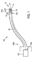
図1は、一実施形態による最小侵襲性の医療器具100の概略図を示す。最小侵襲性の医療器具100(又は最小侵襲性の医療装置とも呼ばれる)は、近位端100b及び遠位端100a(又は遠位先端部とも呼ばれる)を有する。医療侵襲介入において、遠位端100aは、介入が行われる患者の身体の解剖学的部位に配置される。最小侵襲性の医療器具100は、医療器具の遠位端100aに配置されるセンサ装置10を含む。センサ装置10は、電気センサ信号の形でセンサデータを生成するように構成されるセンサ20を含む。センサ20は、電気センサ信号を送信するセンサ出力部21を有する。センサ装置は、電気センサ信号を光学信号に変換するように構成されるデータ変換装置40を更に有する。データ変換装置40は、センサ20から、特にセンサ出力部21から、電気センサ信号を受け取る電気入力部41を有する。センサ出力部21は、電気接続25を通じてデータ変換装置40の電気入力部41に接続される。データ変換装置40は、光学信号を送信する光出力部42を更に有する。センサ装置10は、遠位端100aから近位端100bへ光学信号を送信するように構成される光ファイバ50、特に光ガラスファイバ、を更に有する。例えば、光ファイバ50の長さは、遠位端100aから近位端100bに達するに十分長い。光ファイバ100は、第1の端部50a及び第2の端部50bを有する。光ファイバ50は、光学信号を受け取るために、データ変換装置40の光出力部42に結合される。より具体的には、光ファイバ50の第1の端部50aが、データ変換装置40の出力部42に結合される。光ファイバ50は、医療器具100の遠位端100aから近位端100bまで延在する。光ファイバ50の第2の端部50bは、医療器具100の近位端100bに配置される。こうして、光ファイバは、医療器具100の遠位端100aから近位端100bまでセンサ20の高データレートのセンサデータを送信するために使用される。これは、医療器具100の遠位端100aから及び/又は遠位端100aへの高速光学データリンクを提供する。1つの光ファイバ50のみが図面に示されているが、任意の数又は複数の光ファイバは、使用されることができる。
FIG. 1 shows a schematic diagram of a minimally invasive
図1に示される実施形態において、光ファイバ50の第2の端部50bは、例えば医用イメージングのためにセンサデータ又は電気センサ信号を読み出し及び/又は処理するように構成される信号処理装置120に接続される。例えば、信号処理装置120は、(光ファイバ50から受け取られる)光学信号を電気信号に戻すように変換するように構成されることができる。更に、信号処理装置120は、(例えばアプリケーションによって必要とされる場合)デジタルドメインで電気信号を処理するように構成されることができる。
In the embodiment shown in FIG. 1, the
このような最小侵襲性の医療器具100を製造する対応する方法は、最初に、このようなセンサ装置10を製造するステップを含む。センサ装置10を製造するステップは、センサ20を提供し、データ変換装置40を提供し、光ファイバ50を提供し、データ変換装置40の出力部42に光ファイバ50を結合することを含む。医療器具100を製造する方法は、センサ装置10を医療器具100の遠位端に配置するステップを更に含む。光ファイバ50は、器具100の遠位端100aから近位端100bまで延在する。
A corresponding method of manufacturing such a minimally invasive
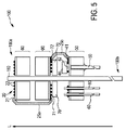
この記述において、図に示されるセンサ20は、超音波を送信し及び/又は受信するように構成される超音波トランスデューサであり、特に容量性マイクロマシン加工超音波トランスデューサ(CMUT)である。これは、特に医用イメージングのために、最小侵襲性の装置にとって特に有用なセンサである。超音波トランスデューサは、多量のセンサデータ(ゆえに高データレート)を生成し、これは、高データレート伝送を必要とする。特に、超音波トランスデューサ20は、互いに隣り合わせで配置される複数の超音波トランスデューサセル22、特にCMUTセルを含む。しかしながら、センサは、画像(例えば患者の身体又はその一部)を表すセンサデータを生成する任意の他の種類の医用イメージングセンサでありうることが理解されるであろう。例えば、センサは、カメラ(例えばCCDチップ又はCMOS画像センサチップ)である。医用イメージングセンサは、多量のセンサデータを、ゆえに高データレートを生成し、これは、高データレート伝送を必要とする。しかしながら、概して他のタイプの任意のセンサ、特に高データレートを生成するセンサが、使用されることができることが理解されるであろう。概して、センサは、圧力センサのような低データレートを生成するセンサでありうる。しかしながら、ここに記述される高速光学データリンクは、超音波トランスデューサ又はカメラのような、特に高データレートを生成するセンサに有用である。
In this description, the
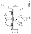
図2は、一実施形態による医療器具100、特に図1に関して説明された医療器具のセンサ装置10の一部の概略断面図を示す。センサ装置10は、特に図1に関して説明されたように、センサ(図2には不図示)、データ変換装置40及び光ファイバ50を有する。センサ装置10は、第1の表面30a及び第2の表面30bを有する基板30(例えばシリコンチップ)を更に含む。データ変換装置40は、第1の基板表面30aに配置され又は取り付けられる。図2に示されるこの実施形態において、光ファイバ50は、基板30の孔34に配置されている。孔34は、第2の基板表面30bから第1の基板表面30aへ向けて延在する。孔34は、基板表面30a、30bに対して垂直に配置される。従って、孔34に配置される光ファイバ50もまた、基板表面30a、30bに対して垂直に配置される。孔34は、光ファイバ50の第1の端部50aがデータ変換装置40の出力部42に結合されるように配置される。言い換えると、データ変換装置40は、第1の基板表面30aへ向けて、光ファイバ50の第1の端部50aが位置する領域に、光学信号を送信するように配置される。光ファイバ50の中心が、光出力部から送信される光学信号又は光のすべてを受信するように、第1の端部50a又は孔34が、光出力部42に中心を合わせるように配される。光ファイバの第2の端部50bは、医療器具の近位端100bに配置される。これを示すために、光ファイバは、図2において切断面で示されている。
FIG. 2 shows a schematic cross-sectional view of a portion of a
図2に示されるこの実施形態において、基板は、(例えばシリコンで作られる)ベース層31、及びベース層31上の第1の絶縁層32(例えば酸化シリコンのような酸化物)を有し、第1の絶縁層32が、第1の基板表面30aを形成する。絶縁層32は、電気的に絶縁している。この第1の絶縁層32を使用することによって、ベース層31が導電性又は半導電性であっても、データ変換装置40への電気接続を提供する電気接続部46が、第1の基板30a上に配置されることができる。例えば、ベース層30は、シリコンで作られることができる。この場合、絶縁層は、シリコンを酸化することによって形成されうる酸化シリコンで作られることができる。任意に、基板30は、ベース層31上に第2の絶縁層33を有することができ、第2の絶縁層33は、図2に示されるように第2の基板表面30bを形成する。
In this embodiment shown in FIG. 2, the substrate has a base layer 31 (eg made of silicon) and a first insulating layer 32 (eg an oxide such as silicon oxide) on the
図2に示されるこの実施形態において、孔34は、第1の基板表面30aを形成する第1の絶縁層32のところで終端する。従って、孔34は、ブラインド孔である。第1の絶縁層32は、光学的に透明である。例えば、酸化シリコンは、光学的に透明である。第1の絶縁層32は、光ファイバ50からデータ変換装置40の光学出力部42を絶縁するが、光学信号が絶縁層32を通過するに十分薄い。光ファイバ50は、基板30に固定的に接続される。言い換えると、光ファイバ50は、基板30に永続的に取り付けられる。こうして、光ファイバ50は、データ変換装置40の出力部42に永続的に結合される。特に、光学的に透明な接着剤52が、光ファイバ50を基板30に固定的に接続するために使用される。図2から分かるように、孔34の残りの空間、特に基板30(又はその絶縁層32)と光ファイバ50との間の空間は、光学的に透明な接着剤52で充填される。これは、光学結合を改善する。更に、図2から分かるように、光学的に透明なアンダーフィル材48が、データ変換装置40と第1の基板表面30aとの間に、特にデータ変換装置40の光出力部42と第1の基板表面30a(又は光ファイバ50の第1の端部50a)との間に、配置される。これは光学結合をより一層改善する。
In this embodiment shown in FIG. 2, the
この記述において、図に示されるデータ変換装置40は、垂直共振器面発光レーザ(VCSEL)である。VCSEL40は、電気センサ信号を入力する電気入力部を有する。図2において、特にセンサ20からデータ変換装置40への電気接続を提供するための電気接続部46は、ソルダーバンプ47によってVCSEL 40又はその入力部に接続される。VCSEL40は、レーザ光を生成する活性領域44を含む。特に、活性領域44は、第1のミラー(又はブラッグ反射体)と、第2のミラー(又はブラッグ反射体)と、第1及び第2のミラーの間に配置されるレーザキャビティ(又は量子井戸)とを含む。VCSEL40は、光出力部42を更に含む。光出力部42は、第1の基板表面30aに対向する。光出力部42は、生成されたレーザ光を受け取り、光学信号としてそれを送信する又は放出する。VCSEL40は、第1の基板表面30aへ向けて光学信号を送信するのに特に有用である。しかしながら、概して、電気センサ信号を光学信号に変換するように構成される任意の他のタイプのデータ変換装置が使用されることができることが理解される。例えば、データ変換装置は、発光ダイオード(LED)又はダイナミックミラー装置(DMD)でありうる。
In this description, the
データ変換装置40は、(光ファイバ50を通じて送信された)光学信号を、(例えばセンサを駆動する及び/又は制御するための)電気信号に変換するようにも構成されることができる。このようにして、データ変換装置40は、信号を両方向に変換することができる。従って、光ファイバ50は、遠位端100aからの及び遠位端100aへの両方において高速光学データリンクを提供する。これは双方向通信を可能にする。前述したようにデータ変換装置がVCSELである場合、例えば、フォトダイオードは、VCSEL又はその活性領域の下に又はそれを囲んで配置される。
The
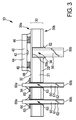
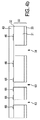
図3は、別の実施形態による医療器具100のセンサ装置10の一部の概略断面図を示す。図3の実施形態は図2の実施形態に基づくので、図2の実施形態についてなされたのと同じ説明が、図3の実施形態にも当てはまる。図3に示される実施形態において、センサ装置10は、付加的に、医療器具100の遠位端100aから近位端100bまで延在する電気ワイヤ60を有する。電気ワイヤ60は、第1の端部60a及び第2の端部60bを含む。第1の端部60aは、センサ装置10に、ゆえに医療器具の遠位端100aに、配置される。第2の端部60bは、医療器具の近位端100bに配置される。これを示すために、電気ワイヤが、図3に切断面で示されている。図3の実施形態において、互いに隣り合って配置される2つの電気ワイヤ60が示される。しかしながら、任意の他の(適切な)数の電気ワイヤが使用されることができる。例えば、電気ワイヤ60は、センサ装置への電力供給のために又は(例えば制御信号の)低速データ伝送のために使用されることができる。
FIG. 3 shows a schematic cross-sectional view of a part of the
電気ワイヤ60は、基板30のスルーホール63を通じて配置され、スルーホール63は、第1の基板表面30aから第2の基板表面30bまで、又はその逆に延在する。光ファイバ50用の孔34及び電気ワイヤ60用のスルーホール63を提供することによって、基板30に対する光ファイバ50及び電気ワイヤ60の同時接続が、例えば1つの処理ステップの中で容易に提供されることができる。電気ワイヤ60は、導電性コア61及びコア61を囲む絶縁体62を含む。絶縁体62は、導電性コア61を電気的に絶縁する。図3から分かるように、電気ワイヤ60又はコア61は、基板30に固定的に接続される。言い換えると、電気ワイヤ60は、基板30に永続的に取り付けられる。第1の端部60bにおいて、電気ワイヤ60は、絶縁フリーな部分を有する。例えば、図3から分かるように、ハンダ接合部64は、第1の端部60aの電気ワイヤ60又はコア61を固定的に基板30に接続するために使用されることができる。図3から分かるように、その第1の端部60aにおける電気ワイヤ60のコア61は、ハンダ接合部64によって、第1の基板表面30a上の電気接続65に接続される。要するに、図3の実施形態において、光ファイバ50及び電気ワイヤ60は、基板に固定して接続される。光ファイバ50は、光学的に透明な接着剤52によって、固定的に接続され、電気ワイヤ60は、ハンダ接合部又は接続部によって固定的に接続される。
The
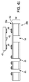
せンサ装置10を製造する方法は、図4a乃至図4dに関して更に詳しく説明される。図4a乃至図4dの各々は、図3のセンサ装置10を製造する方法の異なるステップを示す。センサ装置10の製造は、第1の表面31及び第2の表面30bを有する基板30(例えばシリコンチップ)を提供することから始める。例えば、図4aに示すように、ベース層31(例えばシリコンで作られる)が提供されることができ、例えば酸化シリコンのような酸化物で作られる絶縁層32が、(例えば熱酸化によって)ベース層31に設けられることができる。絶縁層32は、第1の基板表面30aを形成する。センサ20が、第1の基板表面30a上に、より具体的には絶縁層32(図4aには不図示)上に提供されることができる。その後、図4bを参照して、孔34が、(例えばエッチングによって)基板30に設けられ、孔34は、第2の基板表面30bから第1の基板表面30aへ向けて延在する。図4bから分かるように、孔34を設けるステップは、絶縁層32で終わる。この場合、孔34は、第2の基板表面30bから基板ベース層31を通ってエッチングされ、絶縁層32で終了する。図4bに示されるように、更に、スルーホール63が基板30に設けられ、スルーホール63は、第2の基板表面30bから第1の基板表面30aまで延在する。この場合、スルーホール63は、第2の基板表面30bから基板30を貫いてエッチングされる。特に、孔34を設ける(例えばエッチング)ステップ及びスルーホール63を設ける(例えばエッチング)ステップは、1つの処理ステップにおいて実施される。任意には、図4bに示されるように、孔34及びスルーホール63を設ける(例えばエッチングの)とき、サポート層49(例えばポリイミドで作られる)が使用されることができる。
The method of manufacturing the
次に、図4cを参照して、データ変換装置40が提供される。データ変換装置40は、第1の基板表面30a上に配置される。この場合、第1の基板表面30a上に配置される電気接続部46に対して電気接続が設けられる。図4dから分かるように、光ファイバ50が提供される。光ファイバ50(又はその第1の端部50a)が、データ変換装置40の光出力部42に結合される。これは、孔34に光ファイバ50を配置することによって行われる。次に、光ファイバ50を基板30に固定的に接続するために、光学的に透明な接着剤52が、孔34の残りの空間に充填される。最後に、電気ワイヤ60(図3を参照)が提供される。電気ワイヤ60が、スルーホール63を通して配置される。電気ワイヤ60を基板30に固定的に接続するために、ハンダ接合部64が、使用されることができる。上述のステップは、任意の他の適切な順序で実施されることもできることが理解されるであろう。
Next, referring to FIG. 4c, a
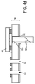
図5は、一実施形態による医療器具100の概略断面図を示し、図5aは、図5の医療器具100の遠位端100aの斜視図を示す。図3を参照して記述されたセンサ装置10の一部が、本実施形態において使用される。従って、以前の実施形態における説明は、図5の実施形態に当てはまる。図5に示される実施形態において、センサ装置10は、電気センサ信号を前処理するように構成される前処理電子回路70を更に有する。従って、前処理は、医療器具100の遠位端100aにおいて行われる。例えば、前処理電子回路70は、電気センサ信号を増幅し及び/又は多重化するように構成されることができる。このようにして、センサ20からの生センサデータ又は信号が、近位端100bに送信される必要はなく、センサデータが前処理されることができる(例えば調整される)。前処理電子回路は、特に、センサ20を制御するために使用される電子回路でありえ、又はかかる電子回路であり、又はその中に組み込まれ、又はその一部でありうる。例えば、前処理電子回路は、特定用途向け集積回路(ASIC)でありうる。前処理電子回路70は、センサ20から電気センサ信号を受け取るための入力部71を含む。特に、前処理電子回路は、センサから電気センサ信号を受け取るための複数の入力ポートを含む。電気接続部25aが、センサ20又はセンサ出力21と、電子回路70又はその入力部71との間に提供される。前処理電子回路70は更に、データ変換装置40に前処理された電気センサ信号を送信するための出力部72を更に有する。電気接続部25bが、電子回路70又はその出力部72と、データ変換装置40又はその入力41との間に提供される。図5の実施形態において(図5a参照)、電気接続部25a、25bは、可撓性の電気接続である。前処理電子回路70は、図1乃至図4を参照して記述された実施形態のいずれかと関連して使用されることもできることが理解されるであろう。
FIG. 5 shows a schematic cross-sectional view of a
更に、図5の実施形態において、センサ20(この場合、超音波トランスデューサセル22)は、医療器具100の長さ方向L(この場合、近位端100bから遠位端100aに向かう方向に規定される)において、データ変換装置40が配置される第1の基板30より上に位置付けられる第2の基板80に配置される。従って、センサ20及びデータ変換装置40は、2つの別個の基板30、80に配置される。更に、前処理電子回路70は、長さ方向Lにおいて、データ変換装置40が配置される第1の基板30より上に位置付けられる第3の基板90に配置される。従って、ここでも、前処理電子回路70及びデータ変換装置40は、2つの別個の基板30、90に配置される。言い換えると、データ変換装置40、センサ20及び前処理電子回路70の各々は、それぞれ別個の基板に配置される。図5の実施形態において、第3の基板90は、第2の基板80の下であって、第1の基板30と第2の基板80との間に位置付けられる。センサ20を有する第2の基板80は、最適なやり方でセンスし又はセンサデータを生成するために、器具100の最も遠位部分に配置される。
Further, in the embodiment of FIG. 5, the sensor 20 (in this case, the ultrasonic transducer cell 22) is defined in the length direction L of the medical device 100 (in this case, from the
更に、図5の実施形態において、医療器具100は、細長いガイドワイヤコア110(例えばステンレス鋼で作られる)を有するガイドワイヤである。図5aから分かるように、第1の基板30、第2の基板80及び第3の基板90の各々は、ガイドワイヤコア110を囲むディスクである。ガイドワイヤは、ガイドワイヤを囲む(例えば、基板30、80、90を囲む)伸縮自在のシースを更に含むことができる。しかしながら、概して、任意の他の適切な最小侵襲性の医療器具が使用されることができることが理解されるであろう。
Further, in the embodiment of FIG. 5, the
図5bは、その製造終了時の図5のセンサ装置10の概略断面図を示す。対応する製造方法は、データ変換装置40が配置される第1の基板30を提供するステップと、センサ20が配置される第2の基板80を提供するステップと、前処理電子回路70が配置される第3の基板90を提供するステップと、を含む。図5bの実施形態において、第1の基板30、第2の基板80及び第3の基板90は、単一の連続する基板から形成される。基板30、80、90は、1つの連続する基板内に別個の孔85、95をエッチングすることによって、互いに分離される。このようにして、基板30、80、90を有するセンサ装置10が、容易に製造されることができる。
FIG. 5b shows a schematic cross-sectional view of the
センサ装置10が図5bに示されるように製造された後、第2の基板80及び第3の基板90は、長さ方向Lにおいて、第1の基板30より上に(図5又は図5aを参照)に各々位置付けられる。可撓性の電気接続部25a、25bが、それぞれ異なる基板30、80、90上のセンサ20、電子回路70、及びデータ変換装置40の間の電気接続を各々提供する。
After the
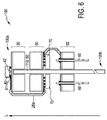
図6は、別の実施形態による医療器具100の概略断面図を示す。図6の実施形態は、光ファイバ50がガイドワイヤコア110を形成するという点で図5の実施形態とは異なる。図5のガイドワイヤコア110は、光ファイバ50によって置き換えられている。こうして、光ファイバ50は、近位端にセンサ20(図6において表示されない)のセンサデータを送信するためだけでなく、ガイドワイヤの機械的コア110又は支持体としても使用される。例えば、図6の実施形態において、センサ20は、1又は複数の基板の周囲に、特にガイドワイヤの外周の周りに沿って曲げられて、配置されることができる。
FIG. 6 shows a schematic cross-sectional view of a
更に、図6の実施形態は、電子回路70を有する第3の基板90が、長さ方向Lにおいて、データ変換装置40を有する第1の基板30の下に位置付けられる点で、図5の実施形態と異なる。光ファイバ50を有する第1の基板30が、医療器具100の最も遠位部分に機械的サポートを提供するために、器具100の最も遠位部分に配置される。
Furthermore, the embodiment of FIG. 6 is that the
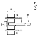
更に、図6の実施形態は、電気ワイヤ60が付加の基板92に配置される点で、図5の実施形態と異なる。従って、データ変換装置40及び電気ワイヤ60は、2つの別個の基板に配置される。付加の基板92は、長さ方向Lにおいて、第1の基板30の下であって且つ第3の基板90の下に位置付けられる。しかしながら、電気ワイヤ60は任意の他の適切なやり方で配置されることもできることが理解されるであろう。例えば、図7は、他の実施形態による医療器具の一部の概略断面図を示す。図7のこの実施形態において、電気ワイヤ60は、データ変換装置40と同じ基板30に配置される。
Furthermore, the embodiment of FIG. 6 differs from the embodiment of FIG. 5 in that
ガイドワイヤがここに記述されているが、最小侵襲性の医療器具は、任意のタイプの最小侵襲性の医療器具でありうることが理解されるであろう。例えば、最小侵襲性の医療器具は、カテーテル、ガイドワイヤ、腹腔鏡器具又は内視鏡でありうる。最小侵襲性の医療器具は、例えば、10000μm又はそれより小さい直径、特に8000μm又はそれより小さい直径、特に3000μm又はそれより小さい直径、特に1000μm又はそれより小さい直径、特に500μm又はそれより小さい直径、特に300μm又はそれより小さい直径を有することができる。具体的な例としては、腹腔鏡器具は、例えば8mm〜3mmの直径を有することができ、カテーテルは、3mm〜1mmの直径を有することができ、及び/又はガイドワイヤは、0.5mm未満の直径を有することができる。例えば、最小侵襲性の医療器具は、スマート医療器具でありうる。スマート医療器具は、その遠位端においてセンサ及びセンサエレクトロニクス(例えばASIC)を含む。 Although guidewires are described herein, it will be appreciated that a minimally invasive medical device can be any type of minimally invasive medical device. For example, the minimally invasive medical instrument can be a catheter, guidewire, laparoscopic instrument, or endoscope. Minimally invasive medical devices are, for example, 10000 μm or smaller diameters, in particular 8000 μm or smaller diameters, in particular 3000 μm or smaller diameters, in particular 1000 μm or smaller diameters, in particular 500 μm or smaller diameters, in particular It can have a diameter of 300 μm or less. As a specific example, the laparoscopic instrument can have a diameter of, for example, 8 mm to 3 mm, the catheter can have a diameter of 3 mm to 1 mm, and / or the guide wire can be less than 0.5 mm. Can have a diameter. For example, a minimally invasive medical device can be a smart medical device. The smart medical device includes a sensor and sensor electronics (eg, ASIC) at its distal end.
本発明は、図面及び上述の記述において詳しく図示され記述されるが、このような図示及び記述は、制限的なものではなく、説明的又は例示的なものとして考えられるべきである。本発明は、開示される実施形態に制限されない。開示される実施形態に対する他の変更が、図面、開示及び添付の特許請求の範囲の検討から、請求項に記載の本発明を実施する際に当業者によって理解され達成されることができる。 While the invention is illustrated and described in detail in the drawings and foregoing description, such illustration and description are to be considered illustrative or exemplary and not restrictive; The invention is not limited to the disclosed embodiments. Other modifications to the disclosed embodiments can be understood and attained by those skilled in the art in practicing the claimed invention, from a study of the drawings, the disclosure, and the appended claims.
請求項において、「含む、有する(comprising)」という語は、他の構成要素又はステップを除外せず、不定冠詞「a」又は「an」は、複数性を除外しない。単一の構成要素又は他のユニットが、請求項に列挙されるいくつかのアイテムの機能を果たすことができる。特定の手段が相互に異なる従属請求項に列挙されているという単なる事実は、これらの手段の組み合わせが有利に使用されることができないことを示さない。 In the claims, the word “comprising” does not exclude other elements or steps, and the indefinite article “a” or “an” does not exclude a plurality. A single component or other unit may fulfill the functions of several items recited in the claims. The mere fact that certain measures are recited in mutually different dependent claims does not indicate that a combination of these measured cannot be used to advantage.
請求項における参照符号は、本発明の範囲を制限するものとして解釈されるべきでない。 Any reference signs in the claims should not be construed as limiting the scope of the invention.
Claims (14)
電気センサ信号の形でセンサデータを生成するセンサと、
前記電気センサ信号を光学信号に変換するデータ変換装置であって、前記電気センサ信号を受け取る電気入力部及び前記光学信号を送信する光出力部を有するデータ変換装置と、
前記遠位端から前記近位端へ前記光学信号を送信する光ファイバであって、前記光学信号を受け取るために前記データ変換装置の出力部に結合され、前記医療器具の前記遠位端から前記近位端まで延在する光ファイバと、
を有し、前記医療器具が、細長いガイドワイヤコアを有するガイドワイヤであり、前記光ファイバが前記ガイドワイヤコアを形成する、医療器具。 A minimally invasive medical device having a proximal end and a distal end, comprising a sensor device disposed at a distal end of the medical device, the sensor device comprising:
A sensor that generates sensor data in the form of electrical sensor signals;
A data converter for converting the electrical sensor signal into an optical signal, the data converter having an electrical input unit for receiving the electrical sensor signal and an optical output unit for transmitting the optical signal;
An optical fiber for transmitting the optical signal from the distal end to the proximal end, coupled to an output of the data converter to receive the optical signal, from the distal end of the medical device; An optical fiber extending to the proximal end;
And the medical device is a guide wire having an elongated guide wire core, and the optical fiber forms the guide wire core.
電気センサ信号の形でセンサデータを生成するセンサを提供するステップと、
電気センサ信号を光学信号に変換するデータ変換装置であって、電気センサ信号を受け取る電気入力部及び光学信号を送信する光出力を有するデータ変換装置を提供するステップと、
前記遠位端から前記近位端まで光学信号を送信する光ファイバを提供するステップと、
光学信号を受け取るために、前記光ファイバを前記データ変換装置の出力部に結合するステップと、
を含み、前記方法が更に、
前記光ファイバが前記医療器具の前記遠位端から前記近位端まで延在するように及び前記光ファイバが前記医療器具のガイドワイヤコアを形成するように、前記センサ装置を前記医療器具の前記遠位端に配するステップ
を含む、方法。 A method of manufacturing a minimally invasive medical device having a proximal end and a distal end, the method comprising manufacturing a sensor device, the manufacturing the sensor device comprising:
Providing a sensor that generates sensor data in the form of electrical sensor signals;
Providing a data converter for converting an electrical sensor signal into an optical signal, the data converter having an electrical input for receiving the electrical sensor signal and an optical output for transmitting the optical signal;
Providing an optical fiber for transmitting an optical signal from the distal end to the proximal end;
Coupling the optical fiber to an output of the data converter to receive an optical signal;
The method further comprising:
The sensor device is positioned on the medical device such that the optical fiber extends from the distal end to the proximal end of the medical device and the optical fiber forms a guide wire core of the medical device. Disposing at the distal end.
Applications Claiming Priority (3)
| Application Number | Priority Date | Filing Date | Title |
|---|---|---|---|
| US201261666958P | 2012-07-02 | 2012-07-02 | |
| US61/666,958 | 2012-07-02 | ||
| PCT/IB2013/055199 WO2014006536A2 (en) | 2012-07-02 | 2013-06-25 | Minimally invasive medical instrument |
Publications (3)
| Publication Number | Publication Date |
|---|---|
| JP2015524285A JP2015524285A (en) | 2015-08-24 |
| JP2015524285A5 JP2015524285A5 (en) | 2016-08-12 |
| JP6198822B2 true JP6198822B2 (en) | 2017-09-20 |
Family
ID=49226201
Family Applications (1)
| Application Number | Title | Priority Date | Filing Date |
|---|---|---|---|
| JP2015519436A Expired - Fee Related JP6198822B2 (en) | 2012-07-02 | 2013-06-25 | Minimally invasive medical device |
Country Status (5)
| Country | Link |
|---|---|
| US (1) | US9730636B2 (en) |
| EP (1) | EP2866673B1 (en) |
| JP (1) | JP6198822B2 (en) |
| CN (1) | CN104519804B (en) |
| WO (1) | WO2014006536A2 (en) |
Families Citing this family (13)
| Publication number | Priority date | Publication date | Assignee | Title |
|---|---|---|---|---|
| JP6633067B2 (en) * | 2015-05-27 | 2020-01-22 | オリンパス株式会社 | Imaging device and endoscope |
| JP7009375B2 (en) | 2016-02-18 | 2022-01-25 | ボストン サイエンティフィック サイムド,インコーポレイテッド | A system for visualizing the target area |
| JPWO2018037551A1 (en) | 2016-08-26 | 2019-06-20 | オリンパス株式会社 | Optical module for endoscope, endoscope, and method of manufacturing optical module for endoscope |
| CN110381796B (en) * | 2017-03-08 | 2022-04-22 | 索尼奥林巴斯医疗解决方案公司 | Medical device and method of manufacturing medical device |
| WO2018173261A1 (en) | 2017-03-24 | 2018-09-27 | オリンパス株式会社 | Endoscope and photoelectric composite module |
| WO2019038929A1 (en) * | 2017-08-25 | 2019-02-28 | オリンパス株式会社 | Endoscope optical module, endoscope, and method for manufacturing endoscope optical module |
| WO2019038930A1 (en) * | 2017-08-25 | 2019-02-28 | オリンパス株式会社 | Endoscope optical module, endoscope, and method for manufacturing endoscope optical module |
| EP3456267A1 (en) * | 2017-09-14 | 2019-03-20 | Koninklijke Philips N.V. | Ultrasound image processing |
| EP3530178A1 (en) * | 2018-02-27 | 2019-08-28 | Koninklijke Philips N.V. | A sensor arrangement for mounting on a guidewire or catheter |
| WO2019207744A1 (en) * | 2018-04-26 | 2019-10-31 | オリンパス株式会社 | Optical module for endoscope, endoscope, and method for manufacturing optical module for endoscope |
| WO2019224942A1 (en) * | 2018-05-23 | 2019-11-28 | オリンパス株式会社 | Endoscope optical module, endoscope, and endoscope optical module manufacturing method |
| TWM576855U (en) * | 2018-12-12 | 2019-04-21 | 榮晶生物科技股份有限公司 | Endoscope device and cable assembly thereof |
| EP4216795A1 (en) * | 2020-09-25 | 2023-08-02 | Boston Scientific Scimed, Inc. | Medical imaging device |
Family Cites Families (21)
| Publication number | Priority date | Publication date | Assignee | Title |
|---|---|---|---|---|
| US6485413B1 (en) * | 1991-04-29 | 2002-11-26 | The General Hospital Corporation | Methods and apparatus for forward-directed optical scanning instruments |
| US6134003A (en) * | 1991-04-29 | 2000-10-17 | Massachusetts Institute Of Technology | Method and apparatus for performing optical measurements using a fiber optic imaging guidewire, catheter or endoscope |
| US5377388A (en) | 1993-12-27 | 1995-01-03 | Decor Concepts, Inc. | Safety cap |
| JPH09122121A (en) * | 1995-10-30 | 1997-05-13 | Omron Corp | In-vivo ultrasonic intensity monitoring device, in-vivo stone crushing treatment device, ultrasonic thermotherapy device, and body insertion instrument posture detection device |
| EP0971626A1 (en) * | 1997-03-06 | 2000-01-19 | Massachusetts Institute Of Technology | Instrument for optically scanning of living tissue |
| WO2001089598A2 (en) * | 2000-05-19 | 2001-11-29 | C.R. Bard, Inc. | Guidewire with viewing capability |
| US7992573B2 (en) * | 2001-06-19 | 2011-08-09 | The Trustees Of The University Of Pennsylvania | Optically guided system for precise placement of a medical catheter in a patient |
| US6798954B2 (en) | 2001-07-24 | 2004-09-28 | 3M Innovative Properties Company | Packaged optical micro-mechanical device |
| JP2003210461A (en) * | 2002-01-22 | 2003-07-29 | Hitachi Cable Ltd | Ultrasound endoscope probe cable |
| US7481793B2 (en) * | 2003-12-10 | 2009-01-27 | Boston Scientic Scimed, Inc. | Modular steerable sheath catheters |
| US6952530B2 (en) | 2003-12-19 | 2005-10-04 | The Aerospace Corporation | Integrated glass ceramic systems |
| US7559925B2 (en) * | 2006-09-15 | 2009-07-14 | Acclarent Inc. | Methods and devices for facilitating visualization in a surgical environment |
| CN101128151A (en) * | 2004-11-02 | 2008-02-20 | 宾夕法尼亚大学受托人 | Optical guidance system for precise placement of medical catheters in patients |
| JP2007260066A (en) * | 2006-03-28 | 2007-10-11 | Pentax Corp | Endoscope device |
| US20070286231A1 (en) * | 2006-05-29 | 2007-12-13 | Pentax Corporation | Optical signal transmitting and receiving apparatus |
| US8934741B2 (en) | 2007-11-16 | 2015-01-13 | Brphotonics Produtos Optoelectronicos LTDA | Integrated circuit with optical data communication |
| US20110144502A1 (en) * | 2009-12-15 | 2011-06-16 | Tea Time Partners, L.P. | Imaging guidewire |
| JP2012069882A (en) | 2010-09-27 | 2012-04-05 | Panasonic Corp | Optical module |
| JP5704878B2 (en) | 2010-09-30 | 2015-04-22 | オリンパス株式会社 | Photoelectric conversion connector, optical transmission module, imaging device, and endoscope |
| JP2013202120A (en) * | 2012-03-27 | 2013-10-07 | Asahi Intecc Co Ltd | Guidewire |
| CA3088574C (en) * | 2012-05-25 | 2023-01-17 | Phyzhon Health Inc. | Optical fiber pressure sensor |
-
2013
- 2013-06-25 JP JP2015519436A patent/JP6198822B2/en not_active Expired - Fee Related
- 2013-06-25 WO PCT/IB2013/055199 patent/WO2014006536A2/en not_active Ceased
- 2013-06-25 US US14/410,621 patent/US9730636B2/en not_active Expired - Fee Related
- 2013-06-25 CN CN201380041326.2A patent/CN104519804B/en not_active Expired - Fee Related
- 2013-06-25 EP EP13765765.6A patent/EP2866673B1/en active Active
Also Published As
| Publication number | Publication date |
|---|---|
| US20150342530A1 (en) | 2015-12-03 |
| CN104519804A (en) | 2015-04-15 |
| WO2014006536A3 (en) | 2014-03-13 |
| JP2015524285A (en) | 2015-08-24 |
| EP2866673A2 (en) | 2015-05-06 |
| WO2014006536A2 (en) | 2014-01-09 |
| EP2866673B1 (en) | 2020-03-18 |
| CN104519804B (en) | 2018-01-30 |
| US9730636B2 (en) | 2017-08-15 |
Similar Documents
| Publication | Publication Date | Title |
|---|---|---|
| JP6198822B2 (en) | Minimally invasive medical device | |
| US9762329B2 (en) | Optical transmission module and imaging device | |
| US11576649B2 (en) | Rotational intravascular ultrasound probe with an active spinning element | |
| JP6334561B2 (en) | Intravascular ultrasound imaging device, interface architecture, and manufacturing method | |
| JP5657673B2 (en) | Small-diameter video camera head and visualization probe and medical devices incorporating them | |
| US8696600B2 (en) | Medical guide wire assembly | |
| JP2006166985A (en) | Ultrasonic probe for internal diagnosis of body cavities and method of making the same | |
| JP6724001B2 (en) | Endoscope system | |
| US20130261467A1 (en) | Method for forming an ultrasound device, and associated apparatus | |
| JP2015524285A5 (en) | ||
| CN109922737A (en) | Wireless intraluminal imaging device and associated devices, systems and methods | |
| CN115316940A (en) | Transparent ultrasonic transducer using beam shaping and method of assembling the same | |
| JP5666873B2 (en) | Ultrasonic diagnostic equipment | |
| US20140257107A1 (en) | Transducer Assembly for an Imaging Device | |
| EP3788937A1 (en) | Sensor arrangement, imaging device, medical device and method of operating a sensor arrangement | |
| JP2010042042A (en) | Ultrasonic diagnostic system | |
| JP2016101317A (en) | Acoustic probe | |
| CN120131075B (en) | Ultrasonic imaging system and equipment | |
| US11876107B2 (en) | Image pickup apparatus for endoscope and endoscope | |
| WO2020179067A1 (en) | Endoscope optical transducer, endoscope imaging device, and endoscope | |
| JP4303008B2 (en) | Solid-state image sensor, electronic endoscope | |
| JP2003210461A (en) | Ultrasound endoscope probe cable | |
| JP4394361B2 (en) | Solid-state image sensor, electronic endoscope | |
| WO2024186918A1 (en) | Mixed array imaging probe | |
| WO2023053954A1 (en) | Optical transmitter module and endoscope |
Legal Events
| Date | Code | Title | Description |
|---|---|---|---|
| A521 | Request for written amendment filed |
Free format text: JAPANESE INTERMEDIATE CODE: A523 Effective date: 20160621 |
|
| A621 | Written request for application examination |
Free format text: JAPANESE INTERMEDIATE CODE: A621 Effective date: 20160621 |
|
| A977 | Report on retrieval |
Free format text: JAPANESE INTERMEDIATE CODE: A971007 Effective date: 20170131 |
|
| RD04 | Notification of resignation of power of attorney |
Free format text: JAPANESE INTERMEDIATE CODE: A7424 Effective date: 20170214 |
|
| A131 | Notification of reasons for refusal |
Free format text: JAPANESE INTERMEDIATE CODE: A131 Effective date: 20170221 |
|
| A521 | Request for written amendment filed |
Free format text: JAPANESE INTERMEDIATE CODE: A523 Effective date: 20170519 |
|
| TRDD | Decision of grant or rejection written | ||
| A01 | Written decision to grant a patent or to grant a registration (utility model) |
Free format text: JAPANESE INTERMEDIATE CODE: A01 Effective date: 20170817 |
|
| A61 | First payment of annual fees (during grant procedure) |
Free format text: JAPANESE INTERMEDIATE CODE: A61 Effective date: 20170822 |
|
| R150 | Certificate of patent or registration of utility model |
Ref document number: 6198822 Country of ref document: JP Free format text: JAPANESE INTERMEDIATE CODE: R150 |
|
| R250 | Receipt of annual fees |
Free format text: JAPANESE INTERMEDIATE CODE: R250 |
|
| R250 | Receipt of annual fees |
Free format text: JAPANESE INTERMEDIATE CODE: R250 |
|
| LAPS | Cancellation because of no payment of annual fees |