JP6198536B2 - Elastic wave device and electronic device using the same - Google Patents
Elastic wave device and electronic device using the same Download PDFInfo
- Publication number
- JP6198536B2 JP6198536B2 JP2013187919A JP2013187919A JP6198536B2 JP 6198536 B2 JP6198536 B2 JP 6198536B2 JP 2013187919 A JP2013187919 A JP 2013187919A JP 2013187919 A JP2013187919 A JP 2013187919A JP 6198536 B2 JP6198536 B2 JP 6198536B2
- Authority
- JP
- Japan
- Prior art keywords
- dielectric film
- electrode fingers
- piezoelectric substrate
- acoustic wave
- electrode
- Prior art date
- Legal status (The legal status is an assumption and is not a legal conclusion. Google has not performed a legal analysis and makes no representation as to the accuracy of the status listed.)
- Active
Links
Images


Description
本発明は、弾性波素子とこれを用いた電子機器に関する。 The present invention relates to an acoustic wave device and an electronic device using the same.
図7に示すように、従来の弾性波素子101は、圧電基板102と、圧電基板102の上に形成されて波長λのレイリー波を主要弾性波として励振する電極指103を有するIDT電極と、圧電基板102の上方にIDT電極の電極指103を覆うように形成された誘電膜104とを備える。
As shown in FIG. 7, a conventional
この誘電膜104として、酸化ケイ素が使用されている。この酸化ケイ素は、圧電基板102の周波数温度係数(TCF:Temperature Coefficient of Frequency)と逆符号の周波数温度係数を有するので、弾性波素子101の周波数温度特性を向上させることができる。
As the
なお、この出願の発明に関する先行技術文献情報としては、例えば、特許文献1が知られている。 As prior art document information relating to the invention of this application, for example, Patent Document 1 is known.
従来の弾性波素子101において、第1誘電膜104が酸化物からなることにより、例えばIDT電極の電極指103の上に第1誘電膜104を形成するときに、IDT電極における電極指103の酸化による腐食が課題となっていた。
In the conventional
そこで、本発明は、IDT電極における電極指の腐食を抑制することを目的とする。 Therefore, an object of the present invention is to suppress electrode finger corrosion in an IDT electrode.
上記目的を達成するために本発明の弾性波素子は、圧電基板と、圧電基板の上方に形成されて主要弾性波を励振させる電極指を有するIDT電極と、圧電基板の上方に電極指を覆うように形成された酸化物からなる第1誘電膜と、電極指の上において、電極指と第1誘電膜との間に形成された非酸化物からなる第2誘電膜と、圧電基板と電極指との間に形成された第3誘電膜とを備え、第3誘電膜を伝搬する横波の速度は前記圧電基板を伝搬する前記主要弾性波の速度よりも速く、IDT電極における隣り合う電極指の間にて、第1誘電膜と第3誘電膜とは接することを特徴とする。 In order to achieve the above object, an acoustic wave device of the present invention includes a piezoelectric substrate, an IDT electrode that is formed above the piezoelectric substrate and has an electrode finger that excites a major acoustic wave, and covers the electrode finger above the piezoelectric substrate. A first dielectric film made of oxide, formed on the electrode finger, a second dielectric film made of non-oxide formed between the electrode finger and the first dielectric film, a piezoelectric substrate and an electrode And a third dielectric film formed between the fingers, and the velocity of the transverse wave propagating through the third dielectric film is faster than the velocity of the main elastic wave propagating through the piezoelectric substrate. The first dielectric film and the third dielectric film are in contact with each other.
本発明の弾性波素子は、電極指の上に形成された非酸化物からなる第2誘電膜によって、例えば電極指の上に第1誘電膜を形成するときに、電極指の酸化が抑制される。すなわち、IDT電極における電極指の腐食が抑制される。 The acoustic wave device of the present invention suppresses oxidation of the electrode finger when the first dielectric film is formed on the electrode finger, for example, by the second dielectric film made of non-oxide formed on the electrode finger. The That is, corrosion of the electrode finger in the IDT electrode is suppressed.
なお、本発明の弾性波素子において、IDT電極における隣り合う電極指の間にて、第3誘電膜に接する誘電膜を第1誘電膜とすることにより、第2誘電膜を形成することによって生じる主要弾性波の周波数変動を抑制している。これにより、該周波数変動による弾性波素子の特性ばらつきを防止することができる。 In the acoustic wave device of the present invention, the second dielectric film is formed by using the first dielectric film as a dielectric film in contact with the third dielectric film between adjacent electrode fingers of the IDT electrode. The frequency fluctuation of the main elastic wave is suppressed. As a result, it is possible to prevent variation in characteristics of the acoustic wave device due to the frequency fluctuation.
(実施の形態1)
以下、本発明の実施の形態1について、図面を用いて説明する。図1は、実施の形態1における弾性波素子の断面模式図(IDT電極の電極指の延伸方向に垂直な断面模式図)である。
(Embodiment 1)
Embodiment 1 of the present invention will be described below with reference to the drawings. FIG. 1 is a schematic cross-sectional view of the acoustic wave device according to Embodiment 1 (cross-sectional schematic view perpendicular to the extending direction of the electrode fingers of the IDT electrode).
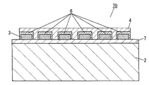
図1において、弾性波素子1は、圧電基板2と、圧電基板2の上に形成されて例えばレイリー波等の表面波を主要弾性波として励振する電極指3を有するIDT電極と、圧電基板2の上方に電極指3を覆うように形成された酸化物からなる第1誘電膜4とを備える。ここで、電極指3のピッチはPである。また、弾性波素子1は、電極指3の上において、電極指3と第1誘電膜4との間に形成された非酸化物からなる第2誘電膜6を備える。さらに、弾性波素子1は、圧電基板2と電極指3との間に形成された第3誘電膜7とを備える。この第3誘電膜7を伝搬する横波の速度Sは圧電基板2を伝搬する主要弾性波の速度よりも速い。これにより、第3誘電膜7による損失を抑制しながら、弾性波素子1の電気機械結合係数をより小さく調整することができ、使用する携帯電話等の通信システムに最適な通過帯域幅を有するフィルタを構成することができる。
In FIG. 1, an acoustic wave element 1 includes a
さらに、またIDT電極における隣り合う電極指3の間にて、第1誘電膜4と第3誘電膜7とは接する。
Further, the first
弾性波素子1は、電極指3の上に形成された非酸化物からなる第2誘電膜6によって、例えば電極指3の上に第1誘電膜4を形成するときに、電極指3の酸化が抑制される。すなわち、IDT電極における電極指3の腐食が抑制される。
When the first
なお、弾性波素子1において、IDT電極における隣り合う電極指3の間にて、第3誘電膜に接する誘電膜を第1誘電膜4とすることにより、第2誘電膜6を形成することによって生じる主要弾性波の周波数変動を抑制している。これにより、該周波数変動による弾性波素子1の特性ばらつきを防止することができる。
In the acoustic wave device 1, the second dielectric film 6 is formed by using the first
圧電基板2は、例えばレイリー波を主要弾性波として伝搬させる圧電基板であるが、SH波(Shear Horizontal波)やバルク波等の他の弾性波を主要弾性波として伝搬させる圧電基板であっても良い。ただし、上記「電極指3間において第3誘電膜7と接して第1誘電膜4を設けることによる主要弾性波の周波数変動の抑制効果」は、圧電基板2がレイリー波を主要弾性波として伝搬させる圧電基板である場合に顕著に現れる。圧電基板2がレイリー波を主要弾性波として伝搬する圧電基板の場合、圧電基板2は、カット角及び主要弾性波の伝搬方向がオイラー角(φ,θ,ψ)表示で、(φ,θ,ψ)=(−10°≦φ≦10°,33°≦θ≦43°,−10°≦ψ≦10°)を満たすニオブ酸リチウム(LiNbO3)系基板、或いは、(φ,θ,ψ)=(−1°≦φ≦1°,113°≦θ≦135°, −5°≦ψ≦5°)の水晶基板、或いは、(φ,θ,ψ)= (−7.5°≦φ≦2.5°,111°≦θ≦121°, −2.5°≦ψ≦7.5°)のタンタル酸リチウム(LiTaO3)系基板である。
The
なお、圧電基板2は、上記以外のオイラー角を有する、水晶、ニオブ酸リチウム(LiNbO3)系、タンタル酸リチウム(LiTaO3)系、或いは、ニオブ酸カリウム(KNbO3)系の基板、又は薄膜など他の圧電媒質であっても構わない。例えば、圧電基板2は、SH波もしくはラブ波を伝搬する−25°〜25°回転Yカットのニオブ酸リチウム、或いはSH波もしくはラブ波を伝搬する25°〜50°回転Yカットのタンタル酸リチウム基板であっても良い。
The
IDT電極は、弾性波素子1の上方からみて対になった櫛形電極の電極指3が噛み合うように圧電基板2上に配置された共振器等を構成する。IDT電極の電極指3は、例えば、アルミニウム、銅、銀、金、チタン、タングステン、モリブデン、白金、又はクロムからなる単体金属、若しくはこれらを主成分とする合金、またはこれらの積層構造である。IDT電極の電極指3が積層構造の場合は、IDT電極の電極指3は、一例として、圧電基板2側から順に、モリブデンを主成分とするMo電極層と、このMo電極層の上に設けられたAlを主成分とするAl電極層とを有する。Mo電極層は相対的に密度が高いので、主要弾性波を圧電基板2の表面に閉じ込めることができ、Al電極層により、IDT電極の電極指3の電気抵抗を下げることができる。このMo電極層にはシリコン等の混合物が混入されていても良いし、Al電極層にはマグネシウム、銅、シリコン等の混合物が混入されていても良い。これにより、IDT電極の電極指3の耐電力性を向上することができる。
The IDT electrode constitutes a resonator or the like disposed on the
このIDT電極の電極指3の総膜厚は、IDT電極の電極指3の総密度bとし、アルミニウムの密度をaとした場合、0.05λ×b/a以上0.15λ×b/a以下であることが望ましい。ここで、λはIDT電極の電極指3のピッチPの2倍で決まる波長である。このときに、弾性波素子1の表面に主要弾性波を集中させることができる。
The total film thickness of the
第1誘電膜4は、酸化物からなる無機絶縁膜である。この第1誘電膜4は、例えば、これを伝搬する横波の速度がIDT電極の電極指3によって励振される主要弾性波の速度より遅い媒質であり、一例として、酸化ケイ素(SiO2)を主成分とする媒質からなる。この酸化ケイ素は、圧電基板2の周波数温度係数(TCF:Temperature Coefficient of Frequency)と逆符号の周波数温度係数を有する。この酸化ケイ素を第1誘電膜4として使用することで、弾性波素子1の周波数温度特性を向上させることができる。
The first
第1誘電膜4が酸化ケイ素の場合、IDT電極の電極指3によって励振される主要弾性波の周波数温度特性の絶対値が所定値(40ppm/℃)以下になるようにその膜厚が設定されている。なお、本実施の形態でいう第1誘電膜4の膜厚とは、隣り合うIDT電極の電極指3の間における第1誘電膜4と第3誘電膜7との境界から第1誘電膜4の上面の距離Hを指す。上記所定値を満たす酸化ケイ素からなる第1誘電膜4の膜厚は、0.2λ以上0.5λ以下である。
When the
第2誘電膜6は、非酸化物からなる無機絶縁膜である。これにより、電極指3の上に第1誘電膜4を形成するときに、電極指3の酸化が抑制される。すなわち、電極指3の腐食が抑制される。この効果は、第2誘電膜6が窒化ケイ素などの窒化物或いは炭化ケイ素などの炭化物からなる無機絶縁膜である場合に顕著に現れる。また、第2誘電膜6は、例えば、これを伝搬する横波の速度がIDT電極の電極指3によって励振される主要弾性波の速度より速い媒質、或いは第1誘電膜4を伝搬する横波の速度より速い媒質であり、一例として、ダイヤモンド膜、窒化ケイ素、酸化窒化ケイ素、窒化アルミニウム、または酸化アルミニウムを主成分とする媒質である。
The second dielectric film 6 is an inorganic insulating film made of a non-oxide. Thereby, when the
第3誘電膜7は、これを伝搬する横波の速度が圧電基板2を伝搬する主要弾性波の速度よりも速い媒質からなる。これにより、第3誘電膜7による損失を抑制しながら、弾性波素子1の電気機械結合係数をより小さく調整することができ、使用する携帯電話等の通信システムに最適な通過帯域幅を有するフィルタを構成することができる。圧電基板2が水晶、ニオブ酸リチウム(LiNbO3)系、タンタル酸リチウム(LiTaO3)系、或いは、ニオブ酸カリウム(KNbO3)系である場合、第3誘電膜7として、酸化アルミニウム(Al2O3)、ダイヤモンド膜、窒化ケイ素、酸化窒化ケイ素、窒化アルミニウム、窒化チタン等を採用すればよい。
The third
また、第3誘電膜7は、その誘電率が圧電基板2の誘電率より小さい媒質でも良い。これにより、弾性波素子1の電気機械結合係数をより小さく調整することができ、使用する携帯電話等の通信システムに最適な通過帯域幅を有するフィルタを構成することができる。圧電基板2がニオブ酸リチウム(LiNbO3)系、タンタル酸リチウム(LiTaO3)系、或いは、ニオブ酸カリウム(KNbO3)系である場合、第3誘電膜7として、酸化アルミニウム(Al2O3)、ダイヤモンド膜、窒化ケイ素、酸化窒化ケイ素、窒化アルミニウム等を採用すればよい。
The third
図2は、比較例の弾性波素子60の断面模式図(IDT電極の電極指の延伸方向に垂直な断面模式図)である。比較例の弾性波素子60は、圧電基板2の上に第3誘電膜7を有し、第3誘電膜7の上に弾性波を励振する電極指3を有し、電極指3が形成されていない第3誘電膜7の上と電極指3の上に非酸化物からなる第2誘電膜5、6を有し、第2誘電膜5、6を覆うように酸化物からなる第1誘電膜4を有する。
FIG. 2 is a schematic cross-sectional view (cross-sectional schematic view perpendicular to the extending direction of the electrode fingers of the IDT electrode) of the
本発明の実施の形態1にかかる弾性波素子1は、比較例の弾性波素子60と比較して、周波数変動による電気特性のばらつきを防止することができる。
The elastic wave device 1 according to the first exemplary embodiment of the present invention can prevent variations in electrical characteristics due to frequency fluctuations as compared with the
図3は、実施の形態1における他の弾性波素子70の断面模式図(IDT電極の電極指の延伸方向に垂直な断面模式図)である。他の弾性波素子70は、図3に示す様に、第2誘電膜6は、IDT電極の電極指3の側面にも形成されていることが望ましい。これにより、第2誘電膜6による電極指3への保護効果を高めることができ、電極指3の酸化が抑制される。
FIG. 3 is a cross-sectional schematic diagram (cross-sectional schematic diagram perpendicular to the extending direction of the electrode finger of the IDT electrode) of another
さらに、電極指3の上における第2誘電膜6の膜厚は電極指3の側面における第2誘電膜6の膜厚より厚いことが望ましい。これにより、第2誘電膜6による電極指3への保護効果をさらに高めることができ、電極指3の酸化が抑制されると共に、第2誘電膜6による主要弾性波の周波数変動の抑制効果を高めることができる。
Further, it is desirable that the film thickness of the second dielectric film 6 on the
図4は、実施の形態1におけるさらに他の弾性波素子80の断面模式図(IDT電極の電極指の延伸方向に垂直な断面模式図)である。さらに他の弾性波素子80は、図4に示すように、IDT電極の電極指3の側面に形成された第2誘電膜6は、側面の上方から側面の一部の領域を覆うように形成されていても良い。これにより、第2誘電膜6による主要弾性波の周波数変動の抑制効果をさらに高めると共に、電極指3の酸化を抑制することができる。
FIG. 4 is a schematic cross-sectional view of another
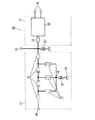
図5は、本実施の形態の弾性波素子1を用いたアンテナ共用器10の回路ブロック図である。図5に示す様に、アンテナ共用器10は、第1通過帯域を有する第1フィルタ11と、第1通過帯域より高い第2通過帯域を有する第2フィルタ12とを備える。
FIG. 5 is a circuit block diagram of the
図5において、アンテナ共用器10は、例えばUMTSシステムのバンド8用のアンテナ共用器で、送信フィルタである第1フィルタ11とこの第1フィルタ11の通過帯域(880MHzから915MHz)の高域側に通過帯域(925MHzから960MHz)を有する受信フィルタである第2フィルタ12とを備える。第1フィルタ11は、入力端子14とアンテナ端子15との間に接続され、送信信号を入力端子14から受けてアンテナ端子15から出力する。この第1フィルタ11は、直列共振器13と、これら直列共振器13の反共振周波数よりも低い共振周波数を有する並列共振器17とを梯子状に接続し構成されている。さらに、並列共振器17のグランド20側はグランド端子19にて接続され、第1フィルタ11はグランド端子19とグランド20との間に接続されたインダクタ18を備える。
In FIG. 5, an
また、第2フィルタ12は、アンテナ端子15と出力端子(バランス端子)16との間に接続された例えば共振器21と縦モード結合型フィルタ22とを備え、受信信号をアンテナ端子15から受けて出力端子16から出力する。
The
また、アンテナ共用器10は、第1フィルタ11と第2フィルタ12との間に接続された移相器23を備え、この移相器23によって、送受信フィルタ間で他方の通過帯域をハイインピーダンスとし互いのアイソレーション向上を図っている。
The
本実施の形態1の弾性波素子1を第1フィルタ11、或いは第2フィルタ12に採用することで、アンテナ共用器10におけるIDT電極の電極指腐食を抑制すると共に、各々のフィルタ11、12における主要弾性波の周波数変動によるアンテナ共用器10の特性ばらつきを防止することができる。
By employing the elastic wave element 1 of the first embodiment for the
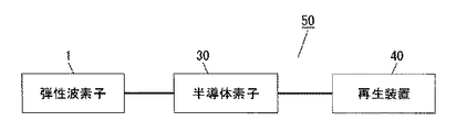
また、図6に示すように、本実施の形態1における携帯電話等の電子機器50は、上記弾性波素子1と、この弾性波素子1に接続された半導体素子30と、この半導体素子30に接続された液晶等の表示部やスピーカ等の音声再生部からなる再生装置40を備える。
As shown in FIG. 6, the
このように本実施の形態1の弾性波素子1を電子機器50に採用することにより、電子機器50の通信品質を向上させることができる。
As described above, by employing the acoustic wave device 1 of the first embodiment in the
本発明にかかる弾性波素子は、弾性波素子の信頼性と量産性を向上させるという効果を有し、携帯電話等の電子機器に適用可能である。 The acoustic wave device according to the present invention has an effect of improving the reliability and mass productivity of the acoustic wave device, and can be applied to an electronic device such as a mobile phone.
1、70、80 弾性波素子
2 圧電基板
3 電極指
4 第1誘電膜
6 第2誘電膜
7 第3誘電膜
10 アンテナ共用器
11 第1フィルタ
12 第2フィルタ
1, 70, 80
Claims (12)
前記圧電基板の上面の上方に配置されたIDT電極であって、レイリー波である主要弾性波を励振させるべく構成された複数の電極指を含むIDT電極と、
前記圧電基板の上面の上方に配置されて前記複数の電極指を覆う酸化物製の第1誘電膜と、
前記複数の電極指の上面に、及び前記第1誘電膜と前記複数の電極指それぞれとの間に配置された非酸化物製の第2誘電膜と、
前記複数の電極指の隣接する電極指間の位置において前記第1誘電膜に接触するように前記圧電基板と前記複数の電極指との間に形成された第3誘電膜と
を含み、
前記第1誘電膜と前記第3誘電膜との接触により、前記第2誘電膜の形成がもたらす主要弾性波の周波数変動が抑制され、
前記第3誘電膜を伝搬する横波の速度は前記圧電基板を伝搬する前記主要弾性波の速度よりも速く、
前記圧電基板は、カット角及び主要弾性波の伝搬方向がオイラー角(φ,θ,ψ)表示で、(φ,θ,ψ)=(−10°≦φ≦10°,33°≦θ≦43°,−10°≦ψ≦10°)を満たすニオブ酸リチウム系基板、(φ,θ,ψ)=(−1°≦φ≦1°,113°≦θ≦135°,−5°≦ψ≦5°)の水晶基板、及び(φ,θ,ψ)=(−7.5°≦φ≦2.5°,111°≦θ≦121°,−2.5°≦ψ≦7.5°)のタンタル酸リチウム系基板からなる群から選択される弾性波素子。 A piezoelectric substrate having an upper surface;
An IDT electrode disposed above an upper surface of the piezoelectric substrate, the IDT electrode including a plurality of electrode fingers configured to excite a major acoustic wave that is a Rayleigh wave ;
A first dielectric film made of an oxide disposed over the upper surface of the piezoelectric substrate and covering the plurality of electrode fingers;
A non-oxide second dielectric film disposed on an upper surface of the plurality of electrode fingers and between the first dielectric film and each of the plurality of electrode fingers;
A third dielectric film formed between the piezoelectric substrate and the plurality of electrode fingers so as to contact the first dielectric film at a position between adjacent electrode fingers of the plurality of electrode fingers;
The contact between the first dielectric film and the third dielectric film suppresses the frequency fluctuation of the main elastic wave caused by the formation of the second dielectric film,
Velocity of transverse wave propagating through the third dielectric film is rather fast than the speed of the primary acoustic wave propagating through the piezoelectric substrate,
In the piezoelectric substrate, the cut angle and the propagation direction of the main elastic wave are represented by Euler angles (φ, θ, ψ), and (φ, θ, ψ) = (− 10 ° ≦ φ ≦ 10 °, 33 ° ≦ θ ≦ 43 °, −10 ° ≦ ψ ≦ 10 °) lithium niobate substrate, (φ, θ, φ) = (− 1 ° ≦ φ ≦ 1 °, 113 ° ≦ θ ≦ 135 °, −5 ° ≦ (φ ≦ θ °) and (φ, θ, φ) = (− 7.5 ° ≦ φ ≦ 2.5 °, 111 ° ≦ θ ≦ 121 °, −2.5 ° ≦ φ ≦ 7. 5 °) acoustic wave element selected from the group consisting of lithium tantalate substrates .
請求項1の弾性波素子と、
前記弾性波素子に接続された再生装置と
を含む電子機器。 Electronic equipment,
An acoustic wave device according to claim 1;
And an electronic device including a reproducing device connected to the acoustic wave element.
前記圧電基板の上面の上方に形成されたIDT電極であって、レイリー波である主要弾性波を励振させるべく構成された複数の電極指を含むIDT電極と、
前記圧電基板の上面の上方に配置されて前記複数の電極指を覆う酸化物製の第1誘電膜と、
前記複数の電極指の上面に、及び前記第1誘電膜と前記複数の電極指それぞれとの間に配置された非酸化物製の第2誘電膜と、
前記複数の電極指の隣接する電極指間の位置において前記第1誘電膜に接触するように前記圧電基板と前記複数の電極指との間に形成された第3誘電膜と
を含み、
前記第1誘電膜と前記第3誘電膜との接触により、前記第2誘電膜の形成がもたらす主要弾性波の周波数変動が抑制され、
前記第3誘電膜の誘電率は前記圧電基板の誘電率よりも小さく、
前記圧電基板は、カット角及び主要弾性波の伝搬方向がオイラー角(φ,θ,ψ)表示で、(φ,θ,ψ)=(−10°≦φ≦10°,33°≦θ≦43°,−10°≦ψ≦10°)を満たすニオブ酸リチウム系基板、(φ,θ,ψ)=(−1°≦φ≦1°,113°≦θ≦135°,−5°≦ψ≦5°)の水晶基板、及び(φ,θ,ψ)=(−7.5°≦φ≦2.5°,111°≦θ≦121°,−2.5°≦ψ≦7.5°)のタンタル酸リチウム系基板からなる群から選択される弾性波素子。 A piezoelectric substrate having an upper surface;
An IDT electrode formed above the upper surface of the piezoelectric substrate, the IDT electrode including a plurality of electrode fingers configured to excite a major acoustic wave that is a Rayleigh wave ;
A first dielectric film made of an oxide disposed over the upper surface of the piezoelectric substrate and covering the plurality of electrode fingers;
A non-oxide second dielectric film disposed on an upper surface of the plurality of electrode fingers and between the first dielectric film and each of the plurality of electrode fingers;
A third dielectric film formed between the piezoelectric substrate and the plurality of electrode fingers so as to contact the first dielectric film at a position between adjacent electrode fingers of the plurality of electrode fingers;
The contact between the first dielectric film and the third dielectric film suppresses the frequency fluctuation of the main elastic wave caused by the formation of the second dielectric film,
Dielectric constant of the third dielectric layer is minor than the dielectric constant of the piezoelectric substrate,
In the piezoelectric substrate, the cut angle and the propagation direction of the main elastic wave are represented by Euler angles (φ, θ, ψ), and (φ, θ, ψ) = (− 10 ° ≦ φ ≦ 10 °, 33 ° ≦ θ ≦ 43 °, −10 ° ≦ ψ ≦ 10 °) lithium niobate substrate, (φ, θ, φ) = (− 1 ° ≦ φ ≦ 1 °, 113 ° ≦ θ ≦ 135 °, −5 ° ≦ (φ ≦ θ °) and (φ, θ, φ) = (− 7.5 ° ≦ φ ≦ 2.5 °, 111 ° ≦ θ ≦ 121 °, −2.5 ° ≦ φ ≦ 7. 5 °) acoustic wave element selected from the group consisting of lithium tantalate substrates .
Priority Applications (4)
| Application Number | Priority Date | Filing Date | Title |
|---|---|---|---|
| JP2013187919A JP6198536B2 (en) | 2013-09-11 | 2013-09-11 | Elastic wave device and electronic device using the same |
| US14/176,149 US9496846B2 (en) | 2013-02-15 | 2014-02-10 | Acoustic wave device and electronic apparatus including same |
| US15/332,279 US10439585B2 (en) | 2013-02-15 | 2016-10-24 | Acoustic wave device including multiple dielectric films |
| US16/545,037 US11863156B2 (en) | 2013-02-15 | 2019-08-20 | Acoustic wave device including multi-layer interdigital transducer electrodes |
Applications Claiming Priority (1)
| Application Number | Priority Date | Filing Date | Title |
|---|---|---|---|
| JP2013187919A JP6198536B2 (en) | 2013-09-11 | 2013-09-11 | Elastic wave device and electronic device using the same |
Publications (3)
| Publication Number | Publication Date |
|---|---|
| JP2015056712A JP2015056712A (en) | 2015-03-23 |
| JP2015056712A5 JP2015056712A5 (en) | 2016-10-27 |
| JP6198536B2 true JP6198536B2 (en) | 2017-09-20 |
Family
ID=52820806
Family Applications (1)
| Application Number | Title | Priority Date | Filing Date |
|---|---|---|---|
| JP2013187919A Active JP6198536B2 (en) | 2013-02-15 | 2013-09-11 | Elastic wave device and electronic device using the same |
Country Status (1)
| Country | Link |
|---|---|
| JP (1) | JP6198536B2 (en) |
Families Citing this family (2)
| Publication number | Priority date | Publication date | Assignee | Title |
|---|---|---|---|---|
| JP6993400B2 (en) * | 2017-02-22 | 2022-01-13 | 株式会社村田製作所 | Surface acoustic wave element |
| JP6957306B2 (en) * | 2017-10-17 | 2021-11-02 | 太陽誘電株式会社 | Elastic wave device and its manufacturing method |
Family Cites Families (12)
| Publication number | Priority date | Publication date | Assignee | Title |
|---|---|---|---|---|
| JPS513183A (en) * | 1974-06-24 | 1976-01-12 | Matsushita Electric Ind Co Ltd | Atsudenseisoshi |
| JPS51101444A (en) * | 1975-03-04 | 1976-09-07 | Murata Manufacturing Co | Danseihyomenhatoransujuusaa |
| JPS529389A (en) * | 1975-07-14 | 1977-01-24 | Toshiba Corp | Surface acoustic wave device |
| DE19548051A1 (en) * | 1995-12-21 | 1997-06-26 | Siemens Matsushita Components | Electronic component, in particular component working with surface acoustic waves - SAW component - |
| JP3858312B2 (en) * | 1996-11-11 | 2006-12-13 | 松下電器産業株式会社 | Surface acoustic wave device and manufacturing method thereof |
| JP2008067289A (en) * | 2006-09-11 | 2008-03-21 | Fujitsu Media Device Kk | Surface acoustic wave device and filter |
| JP2008109413A (en) * | 2006-10-25 | 2008-05-08 | Fujitsu Media Device Kk | Elastic wave device and filter |
| JP2011135245A (en) * | 2009-12-24 | 2011-07-07 | Panasonic Corp | Elastic wave device, manufacturing method thereof, and electronic device using the same |
| WO2012098816A1 (en) * | 2011-01-18 | 2012-07-26 | 株式会社村田製作所 | Elastic surface wave filter device |
| JP5671713B2 (en) * | 2011-03-04 | 2015-02-18 | スカイワークス・パナソニック フィルターソリューションズ ジャパン株式会社 | Elastic wave device |
| JP5751887B2 (en) * | 2011-03-30 | 2015-07-22 | 京セラ株式会社 | Elastic wave device and elastic wave device using the same |
| JP5859355B2 (en) * | 2012-03-23 | 2016-02-10 | 京セラ株式会社 | Elastic wave device and elastic wave device using the same |
-
2013
- 2013-09-11 JP JP2013187919A patent/JP6198536B2/en active Active
Also Published As
| Publication number | Publication date |
|---|---|
| JP2015056712A (en) | 2015-03-23 |
Similar Documents
| Publication | Publication Date | Title |
|---|---|---|
| JP5828032B2 (en) | Elastic wave element and antenna duplexer using the same | |
| US11863156B2 (en) | Acoustic wave device including multi-layer interdigital transducer electrodes | |
| KR102250789B1 (en) | Acoustic wave devices, high-frequency front-end circuits and communication devices | |
| JP4917396B2 (en) | Filters and duplexers | |
| JP6025815B2 (en) | Surface acoustic wave filter device | |
| JP5182459B2 (en) | Ladder type acoustic wave filter and antenna duplexer using the same | |
| JPWO2020130128A1 (en) | Elastic wave device, duplexer and communication device | |
| JP2008067289A (en) | Surface acoustic wave device and filter | |
| JPWO2011158445A1 (en) | Elastic wave element | |
| JP5891198B2 (en) | Antenna duplexer and electronic device using the same | |
| JP2020188408A (en) | Surface acoustic wave device, filter circuit, and electronic component | |
| JP2014175885A (en) | Acoustic wave element and electronic apparatus using the same | |
| KR20190092557A (en) | Acoustic Wave Device, High Frequency Front End Circuit and Communication Device | |
| CN113454912B (en) | Elastic wave device | |
| JP2023036845A (en) | Acoustic wave device | |
| JP5810113B2 (en) | Elastic wave resonator and elastic wave filter and antenna duplexer using the same | |
| JP6198536B2 (en) | Elastic wave device and electronic device using the same | |
| US11863155B2 (en) | Surface acoustic wave element | |
| JPWO2018164210A1 (en) | Elastic wave device, multiplexer, high-frequency front-end circuit, and communication device | |
| JP2007036344A (en) | Elastic boundary wave apparatus | |
| JPWO2010125934A1 (en) | Elastic wave device | |
| US20160226464A1 (en) | Acoustic wave elements, and duplexers and electronic devices using same | |
| JP2014192676A (en) | Acoustic wave element | |
| JP2006157557A (en) | Surface acoustic wave device |
Legal Events
| Date | Code | Title | Description |
|---|---|---|---|
| A521 | Request for written amendment filed |
Free format text: JAPANESE INTERMEDIATE CODE: A523 Effective date: 20160907 |
|
| A621 | Written request for application examination |
Free format text: JAPANESE INTERMEDIATE CODE: A621 Effective date: 20160907 |
|
| A871 | Explanation of circumstances concerning accelerated examination |
Free format text: JAPANESE INTERMEDIATE CODE: A871 Effective date: 20160907 |
|
| A975 | Report on accelerated examination |
Free format text: JAPANESE INTERMEDIATE CODE: A971005 Effective date: 20161007 |
|
| A131 | Notification of reasons for refusal |
Free format text: JAPANESE INTERMEDIATE CODE: A131 Effective date: 20161220 |
|
| A521 | Request for written amendment filed |
Free format text: JAPANESE INTERMEDIATE CODE: A523 Effective date: 20170216 |
|
| A131 | Notification of reasons for refusal |
Free format text: JAPANESE INTERMEDIATE CODE: A131 Effective date: 20170404 |
|
| A521 | Request for written amendment filed |
Free format text: JAPANESE INTERMEDIATE CODE: A523 Effective date: 20170511 |
|
| TRDD | Decision of grant or rejection written | ||
| A01 | Written decision to grant a patent or to grant a registration (utility model) |
Free format text: JAPANESE INTERMEDIATE CODE: A01 Effective date: 20170808 |
|
| A61 | First payment of annual fees (during grant procedure) |
Free format text: JAPANESE INTERMEDIATE CODE: A61 Effective date: 20170822 |
|
| R150 | Certificate of patent or registration of utility model |
Ref document number: 6198536 Country of ref document: JP Free format text: JAPANESE INTERMEDIATE CODE: R150 |
|
| R250 | Receipt of annual fees |
Free format text: JAPANESE INTERMEDIATE CODE: R250 |
|
| R250 | Receipt of annual fees |
Free format text: JAPANESE INTERMEDIATE CODE: R250 |
|
| R250 | Receipt of annual fees |
Free format text: JAPANESE INTERMEDIATE CODE: R250 |
|
| R250 | Receipt of annual fees |
Free format text: JAPANESE INTERMEDIATE CODE: R250 |