JP6186037B2 - Game machine - Google Patents
Game machine Download PDFInfo
- Publication number
- JP6186037B2 JP6186037B2 JP2016086009A JP2016086009A JP6186037B2 JP 6186037 B2 JP6186037 B2 JP 6186037B2 JP 2016086009 A JP2016086009 A JP 2016086009A JP 2016086009 A JP2016086009 A JP 2016086009A JP 6186037 B2 JP6186037 B2 JP 6186037B2
- Authority
- JP
- Japan
- Prior art keywords
- control device
- master
- decoration
- connection line
- data
- Prior art date
- Legal status (The legal status is an assumption and is not a legal conclusion. Google has not performed a legal analysis and makes no representation as to the accuracy of the status listed.)
- Active
Links
Images


Landscapes
- Pinball Game Machines (AREA)
Description
本発明は、グループに分割された演出装置を制御する複数の単位制御手段と、複数の単位制御手段を制御する統括制御手段とを備える遊技機に関する。 The present invention is related to a gaming machine comprising a plurality of single-level control means for controlling the effect device which is divided into groups, and a plurality of units of the control unit Batch integration that controls the control means.
サブ中継基板と電飾基板との間の配線を簡素化することができる遊技機として、トップ
電飾領域の中央部に配置されたトップLED中央基板をサブ中継基板とシリアル接続し、
トップ電飾領域の右側部に配置されたトップLED右基板及びトップ電飾領域の左側部に
配置されたトップLED左基板をトップLED中央基板から分離して配線により接続した
構成の遊技機が知られている。これにより、サブ中継基板からトップ電飾領域への配線数
を減らして配線を簡素化することができる(例えば、特許文献1参照)。
As a gaming machine that can simplify the wiring between the sub relay board and the electrical decoration board, the top LED central board arranged in the center of the top electrical decoration area is serially connected to the sub relay board,
A gaming machine having a configuration in which a top LED right substrate disposed on the right side of the top illumination area and a top LED left substrate disposed on the left side of the top illumination area are separated from the top LED central substrate and connected by wiring. It has been. Thereby, the number of wirings from the sub relay board to the top illumination area can be reduced to simplify the wiring (for example, see Patent Document 1).
また、信号線の数を削減することができると共に不正行為の発見を容易に行うことがで
きる遊技機として、主基板と副基板との間での信号送信をI2Cバス方式により行い、主
基板及び副基板にそれぞれ双方向バスバッファを設けたものがある。この双方向バスバッ
ファは、I2Cバスを構成する二つの双方向シリアルライン(SDA、SCL)をそれぞ
れ二つの片方向シリアルラインに分岐させるためのものであり、主基板に設けられた双方
向バスバッファと副基板に設けられた双方向バスバッファとの間を、それらによって分岐
された片方向シリアルラインの信号伝送方向が互いに一致するようにして、四つのシリア
ル線で接続した構成としている(例えば、特許文献2参照)。
In addition, as a gaming machine that can reduce the number of signal lines and easily detect fraudulent activities, signal transmission between the main board and the sub board is performed by the I 2 C bus method. Some boards and sub-boards are each provided with a bidirectional bus buffer. This bidirectional bus buffer is for bifurcating the two bidirectional serial lines (SDA, SCL) constituting the I 2 C bus into two unidirectional serial lines, respectively. The bus buffer and the bidirectional bus buffer provided on the sub-board are connected by four serial lines so that the signal transmission directions of the one-way serial lines branched by them match each other ( For example, see Patent Document 2).
従来の遊技機では、配線を十分に削減することができなかった。 In conventional gaming machines, the wiring could not be reduced sufficiently .
本発明は、複数の演出装置を複数グループに分割し、演出装置を制御する単位制御手段をグループ毎に備えるとともに、前記単位制御手段の各々を統括的に制御する統括制御手段を備え、前記統括制御手段と前記単位制御手段との間に、データ線とタイミング信号線が接続されて、前記統括制御手段から前記単位制御手段にデータ伝達を可能とし、前記統括制御手段は、前記演出装置の制御に関わる演算処理を行う演算処理手段と、前記単位制御手段と接続されて、前記演算処理手段からの指令に基づいて、該単位制御手段との間の前記データ線及び前記タイミング信号線の各信号レベルを制御する信号レベル制御手段と、を含んで構成され、前記演算処理手段による演算処理と前記信号レベル制御手段による各信号レベルの制御とが、各々並行して実行可能であり、前記統括制御手段が送信するデータには、前記演出装置の出力態様を規定する演出態様情報と、前記単位制御手段が前記演出装置の出力態様を更新させるタイミングを規定する更新規定情報が含まれ、前記統括制御手段は、前記演出態様情報の送信毎に、前記更新規定情報を前記単位制御手段に送信し、前記単位制御手段は、当該単位制御手段のアドレスを設定可能なアドレス設定手段を備え、前記統括制御手段から送信される更新規定情報に規定されるタイミングで、前記演出装置の出力態様を前記演出態様情報によって規定される出力態様に更新し、前記信号レベル制御手段及び前記単位制御手段は、自身に電源供給が開始されると、自身を初期化する初期化手段を備えたことを特徴とする。 The present invention divides a plurality of effect devices into a plurality of groups, and includes unit control means for controlling the effect devices for each group, and also includes overall control means for comprehensively controlling each of the unit control means. A data line and a timing signal line are connected between the control means and the unit control means to enable data transmission from the overall control means to the unit control means, and the overall control means controls the rendering device. Arithmetic processing means for performing arithmetic processing related to the unit, and connected to the unit control means, based on a command from the arithmetic processing means, each signal of the data line and the timing signal line between the unit control means Signal level control means for controlling the level, and arithmetic processing by the arithmetic processing means and control of each signal level by the signal level control means, respectively The data transmitted by the overall control means defines production mode information that defines the output mode of the rendering device and the timing at which the unit control unit updates the output mode of the rendering device. Update regulation information is included, and the overall control means transmits the update regulation information to the unit control means every time the presentation mode information is transmitted, and the unit control means sets the address of the unit control means. An address setting unit capable of updating the output mode of the rendering device to the output mode defined by the rendering mode information at a timing defined in the update regulation information transmitted from the overall control unit, and the signal level The control unit and the unit control unit include an initialization unit that initializes itself when power supply is started .
本発明によれば、統括制御手段と単位制御手段との間の配線を削減することができる。 According to the present invention, wiring between the overall control unit and the unit control unit can be reduced .
以下、本発明の実施の形態について、図面を参照しながら説明する。 Hereinafter, embodiments of the present invention will be described with reference to the drawings.
図1は、本発明の実施の形態の遊技機1の説明図である。
FIG. 1 is an explanatory diagram of a
遊技機1の前面枠(遊技枠)3は、本体枠(外枠)2にヒンジ4を介して、遊技機1の
前面に開閉回動可能に組み付けられる。前面枠3の表側には、遊技盤10(図2参照)が
収装される。また、前面枠3には、遊技盤10の前面を覆うカバーガラス(透明部材)を
備えたガラス枠18が取り付けられている。
A front frame (game frame) 3 of the
ガラス枠18のカバーガラスの周囲には、装飾光が発光される装飾部材9a、9bが備
えられている。装飾部材9a、9bの内部にはランプやLED等からなる装飾装置が備え
られている。装飾装置を所定の発光態様によって発光させることによって、装飾部材9a
、9bが所定の発光態様によって発光する。
Around the cover glass of the
9b emit light according to a predetermined light emission mode.
ガラス枠18の左右には、音響(例えば、効果音)を発するスピーカ30が備えられて
いる。また、ガラス枠18の上方には照明ユニット11が備えられている。
照明ユニット11には、第1可動式照明13及び第2可動式照明14が左右に配置され
ている。第1可動式照明13及び第2可動式照明14には、LEDなどの照明部材の他に
、照明駆動第1モータ(MOT)13a及び照明駆動第2モータ(MOT)14aが備え
られており、演出内容に応じて動作するように制御される。
In the
照明ユニット11の右下方には、遊技機1において異常が発生したことを報知するため
の異常報知LED29が備えられている。
An
前面枠3の下部の開閉パネル20には図示しない打球発射装置に遊技球を供給する上皿
が、固定パネル22には下皿23及び打球発射装置の操作部24等が備えられる。下皿2
3には、下皿23に貯まった遊技球を排出するための下皿球抜き機構16が備えられる。
前面枠3下部右側には、ガラス枠18を施錠するための鍵25が備えられている。
The open /
3 is provided with a lower tray
A key 25 for locking the
また、遊技者が操作部24を回動操作することによって、打球発射装置は、上皿21か
ら供給される遊技球を発射する。
Further, when the player turns the
また、上皿21の上縁部には、遊技者からの操作入力を受け付けるための演出ボタン1
7が備えられている。遊技者が演出ボタン17を操作することによって、遊技盤10に設
けられた表示装置53(図2参照)における特図変動表示ゲームの演出内容を選択して、
表示装置53における特図変動表示ゲームに、遊技者の操作を介入させた演出を行うこと
ができる。
In addition, an
7 is provided. When the player operates the
It is possible to produce an effect in which the player's operation is intervened in the special figure variation display game on the
特図変動表示ゲームは、発射された遊技球が遊技盤10に備わる始動口36(図2参照
)に入賞した場合に開始される。特図変動表示ゲームでは、表示装置53において複数の
識別情報が変動表示する。そして、変動表示していた識別情報が停止し、停止した識別情
報の結果態様が特定の結果態様である場合に、遊技機1の状態が遊技者に有利な状態(特
典が付与される状態)である特別遊技状態に遷移する。
The special figure variation display game is started when the launched game ball wins a start opening 36 (see FIG. 2) provided in the
上皿21の右上部には、遊技者が遊技球を借りる場合に操作する球貸ボタン26、及び
、図示しないカードユニットからプリペイドカードを排出させるために操作される排出ボ
タン27が設けられている。さらに、これらの球貸ボタン26と排出ボタン27との間に
は、プリペイドカードの残高を表示する残高表示部28が設けられる。
In the upper right portion of the
図2は、本発明の実施の形態の遊技盤10の正面図である。
FIG. 2 is a front view of the
図1に示す遊技機1は、内部の遊技領域10a内に遊技球を発射して(弾球して)遊技
を行うもので、ガラス枠18のカバーガラスの奥側には、遊技領域10aを構成する遊技
盤10が設置されている。
The
遊技盤10は、各種部材の取付ベースとなる平板状の遊技盤本体10b(木製又は合成
樹脂製)を備え、該遊技盤本体10bの前面にガイドレール32で囲まれた遊技領域10
aを有している。また、遊技盤本体10bの前面であってガイドレール32の外側には、
前面構成部材33が取り付けられている。そして、このガイドレール32で囲まれた遊技
領域10a内に発射装置から遊技球(打球;遊技媒体)を発射して遊技を行う。
The
a. In addition, on the outside of the
A front
遊技領域10aの略中央には、特図変動表示ゲームの表示領域となる窓部52を形成す
るセンターケース51が取り付けられている。センターケース51に形成された窓部52
の後方には、複数の識別情報を変動表示する特図変動表示ゲームの演出を実行可能な演出
表示装置としての表示装置53が配される。表示装置53は、例えば、液晶ディスプレイ
を備え、表示内容が変化可能な表示部53aがセンターケース51の窓部52を介して遊
技盤10の前面側から視認可能となるように配されている。なお、表示装置53は、液晶
ディスプレイを備えるものに限らず、EL、CRT等のディスプレイを備えるものであっ
てもよい。
A
Behind is a
また、センターケース51の上部には、大当たりの可能性(信頼度)を報知する信頼度
報知装置15が備えられる。信頼度報知装置15には、複数色のLED(例えば、赤、青
、緑の3色のLED)が備えられており、信頼度に応じた色及び態様で発光するように制
御される。
In addition, a
さらに、センターケース51の左部には、遊技球が流下可能な球導入路(ワープ流路)
50が設けられ、遊技領域10aに向けて入口50aが開放した状態で開設されている。
球導入路50は、センターケース51の内部に連通しており、入口50aから流入した遊
技球は、センターケース51の裏側を通過して、ユニット側ステージ部49b上に排出さ
れる。さらに、ユニット側ステージ部49b上で転動した遊技球が当該ユニット側ステー
ジ部49bの下方に配置されたベース側ステージ部49a上に流下できるように構成され
ている。
Furthermore, on the left side of the
50 is provided, and the
The
センターケース51の周縁部には、複数の装飾具47が配置される。センターケース5
1の左下部には、装飾ランプ48が配置される、センターケース51の上部には、複数の
装飾ピース46を上下動可能な状態で配置される。装飾具47、装飾ランプ48及び装飾
ピース46は、後述する演出制御装置550からの命令に従って演出動作を行う。センタ
ーケース51の構成については、図3を参照しながらさらに詳細に説明する。
A plurality of
A
また、遊技領域10aのうちセンターケース51の下方には、遊技球を受入可能(入賞
可能)な特図変動表示ゲームを始動させるための始動口36が配置される。さらに、セン
ターケース51の側方(左側方)には、普図変動表示ゲームを始動させるための普図始動
ゲート34が配置される。
Further, in the
さらに、遊技領域10aには、センターケース51の左下方及び右下方に、発光によっ
て各種装飾表示を行うサイドランプ45が配置される。また、サイドランプ45には、一
般入賞口44が備えられている。
Further, in the
さらに、始動口36の下方には大入賞口42が配置され、該大入賞口42の下方であっ
て遊技領域10aの下縁部には、入賞せずに流下した遊技球を回収するアウト口43が開
設される。大入賞口42は、上端側が手前側に倒れる方向に回動して開放可能になってい
るアタッカ形式の開閉扉42aを備える。特図変動表示ゲームの結果によって開閉扉42
aを閉じた状態(遊技者にとって不利な状態)から開放状態(遊技者にとって有利な状態
)に変換する。
Further, a big winning
a is changed from a closed state (a disadvantageous state for the player) to an open state (a state advantageous to the player).
また、センターケース51、始動口36やサイドランプ45等の取付部分を除いた遊技
領域10a内には、この他、遊技領域10aには、打球方向変換部材としての風車(図示
略)、及び多数の障害釘(図示略)などが配設されている。そして、センターケース51
と、該センターケース51を挟んで普図始動ゲート34とは反対側に位置する前面構成部
材33との間に縦長な円弧状の遊技球通路57が形成されている。
In addition, in the
A longitudinal arc-shaped
さらに、遊技盤10には、特図変動表示ゲーム及び普図変動表示ゲームを実行する普図
・特図表示器35が備えられている。普図・特図表示器35には、特図変動表示ゲームの
未処理回数(特図始動記憶数)及び普図変動表示ゲームの未処理回数(普図始動記憶数)
が表示される。普図・特図表示器35は、遊技状態を表す遊技状態表示LED(図示略)
と併せて、セグメントLEDとして設けられている。
Further, the
Is displayed. The multi-use / special-
In addition, it is provided as a segment LED.
普図始動ゲート34内には、該普図始動ゲート34を通過した遊技球を検出するための
ゲートSW34a(図9参照)が設けられている。そして、遊技領域10a内に打ち込ま
れた遊技球が普図始動ゲート34内を通過すると、普図変動表示ゲームが開始される。
A
また、普図変動表示ゲームを開始できない状態で、普図始動ゲート34を遊技球が通過
すると、普図始動記憶数が上限数未満であるならば、普図始動記憶数が1加算されて、当
該普図変動表示ゲームが当りとなるか否かを示す乱数が普図始動記憶として一つ記憶され
る。
In addition, when the game ball passes through the general chart start
普図変動表示ゲームが開始できない状態とは、例えば、普図変動表示ゲームが既に行わ
れ、その普図変動表示ゲームが終了していない状態や、普図変動表示ゲームに当選して始
動口36が開状態に変換されている状態のことをいう。
The state in which the general map change display game cannot be started is, for example, a state in which the general map change display game has already been performed and the normal map change display game has not been completed, Is the state that has been converted to the open state.
なお、普図変動表示ゲームは、表示装置53の表示領域の一部で普図変動表示ゲームを
表示するようにしてもよく、この場合は識別図柄として、例えば、数字、記号、キャラク
タ図柄などを用い、この識別図柄を所定時間変動表示させた後、停止表示させることによ
って行うようにする。
It should be noted that the universal map change display game may display the universal map change display game in a part of the display area of the
普図変動表示ゲームの停止表示が特別の結果態様となった場合には、普図変動表示ゲー
ムに当選したものとして、始動口36の開閉部材36aが所定時間(例えば、0.5秒間
)開放される。これにより、始動口36に遊技球が入賞しやすくなり、特図変動表示ゲー
ムの始動が容易となる。始動口36の開閉部材36aは、通常時は遊技球の直径程度の間
隔をおいて閉じた状態(遊技者にとって不利な状態)を保持しているが、普図変動表示ゲ
ームの結果が所定の停止表示態様となった場合(普図変動表示ゲームに当選した場合)に
は、ソレノイド(普電SOL36b、図9参照)によって、逆「ハ」の字状に開いて始動
口36に遊技球が流入し易い状態(遊技者にとって有利な状態)に変化させられる。
When the stop display of the normal map change display game becomes a special result mode, the opening / closing
また、本発明の実施の形態の遊技機1は、特図変動表示ゲームの結果態様に基づいて、
遊技状態として、表示装置53における特図変動表示ゲームの変動表示時間を短縮する時
短動作状態(第2動作状態)を発生可能となっている。時短動作状態(第2動作状態)は
、通常動作状態(第1動作状態)と比較して始動口36の開閉部材36aが開放状態とな
りやすい状態である。
In addition, the
As the gaming state, it is possible to generate a short time operation state (second operation state) that shortens the variation display time of the special figure variation display game on the
時短動作状態においては、普図変動表示ゲームの実行時間が通常動作状態における実行
時間よりも短くなるように制御され(例えば、10秒が1秒)、単位時間当りの始動口3
6の開放回数が実質的に多くなるように制御される。また、時短動作状態においては、普
図変動表示ゲームに当選したことによって始動口36が開放される場合に、開放時間が通
常動作状態の開放時間よりも長くなるように制御される(例えば、0.3秒が1.8秒)
。また、時短動作状態においては、普図変動表示ゲームの1回の当選結果に対して、始動
口36が1回ではなく、複数回(例えば、2回)開放される。さらに、時短動作状態にお
いては普図変動表示ゲームの当選結果となる確率が通常動作状態よりも高くなるように制
御される。すなわち、通常動作状態よりも始動口36の開放回数が増加され、始動口36
に遊技球が入賞しやすくなり、特図変動表示ゲームの始動が容易となる。
In the short-time operation state, the execution time of the normal variation display game is controlled to be shorter than the execution time in the normal operation state (for example, 10 seconds is 1 second), and the
The number of times of
. Further, in the short-time operation state, the
This makes it easier for a game ball to win and makes it easier to start a special figure variation display game.
また、始動口36の内部には、始動口36を通過した遊技球を検出するための、始動口
SW36d(図9参照)が備えられる。始動口SW36dによって遊技球を検出すると、
補助遊技としての特図変動表示ゲームを開始する始動権利が発生する。このとき、特図変
動表示ゲームを開始する始動権利は、所定の上限数(例えば4)の範囲内で特図始動記憶
として記憶される。
In addition, a start port SW 36 d (see FIG. 9) for detecting a game ball that has passed through the
A start right to start a special figure variation display game as an auxiliary game is generated. At this time, the right to start the special figure variation display game is stored as a special figure start memory within a predetermined upper limit number (for example, 4).
特図変動表示ゲームを直ちに開始できない状態、例えば、既に特図変動表示ゲームが行
われ、その特図変動表示ゲームが終了していない状態や、特別遊技状態となっている場合
に、始動口36に遊技球が入賞すると、特図始動記憶数が上限数未満(例えば、4個未満
)ならば、特図始動記憶数が1加算され、始動口36に遊技球が入賞したタイミングで抽
出された乱数が特図始動記憶として一つ記憶される。そして、特図変動表示ゲームが開始
可能な状態となると、特図始動記憶に基づき特図変動表示ゲームが開始される。
When the special figure fluctuation display game cannot be started immediately, for example, when the special figure fluctuation display game has already been performed and the special figure fluctuation display game has not been completed, or when the special game state has been entered, the
補助遊技としての特図変動表示ゲームは、遊技盤10に設けられた普図・特図表示器3
5で実行され、複数の識別情報を変動表示したのち、所定の結果態様を停止表示すること
で行われる。また、表示装置53にて特図変動表示ゲームに対応して複数種類の識別情報
(例えば、数字、記号、キャラクタ図柄など)が変動表示される。そして、特図変動表示
ゲームの結果として、普図・特図表示器35の表示態様が特別結果態様となった場合には
、大当たりとなって特別遊技状態(いわゆる、大当たり状態)となる。また、これに対応
して表示装置53の表示態様も特別結果態様(例えば、「7,7,7」等のゾロ目数字の
何れか)となる。なお、普図・特図表示器35ではなく、表示装置53のみで特図変動表
示ゲームを実行するように構成してもよい。
The special figure variation display game as an auxiliary game is a general figure /
This process is executed by stopping and displaying a predetermined result form after a plurality of pieces of identification information are variably displayed. Further, a plurality of types of identification information (for example, numbers, symbols, character designs, etc.) are displayed in a variable manner on the
また、本発明の実施の形態の遊技機1は、特図変動表示ゲームの結果態様に基づき、遊
技状態として確変状態(第2確率状態)を発生可能となっている。この確変状態(第2確
率状態)は、特図変動表示ゲームでの当り結果となる確率が、通常確率状態(第1確率状
態)に比べて高い状態である。なお、確変状態と上述した時短動作状態はそれぞれ独立し
て発生可能であり、両方を同時に発生することも可能であるし、一方のみを発生させるこ
とも可能である。
Further, the
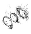
図3は、本発明の実施の形態のセンターケース51の分解斜視図である。
FIG. 3 is an exploded perspective view of the
センターケース51は、遊技盤本体10b(遊技盤10)の表面側に前面構成部として
配置される枠装飾部65と、遊技盤本体10bの裏面側に裏面構成部として配置される枠
体基部60とを前後に重合して構成されている。枠装飾部65は、遊技盤本体10bの表
面に止着される環状の装飾ベース66を備える。装飾ベース66の裏面側には、装飾ベー
ス66と略同じ大きさで円形状に形成された装飾パネルユニット67を備え、枠装飾部6
5は、装飾ベース66と装飾パネルユニット67とを前後に重合して構成されている。
The
5 is configured by superposing a
装飾ベース66の下部には、上面に遊技球を前後方向及び左右方向に転動可能なベース
側ステージ部49aが配置され、該ベース側ステージ部49aと遊技球通路57との間に
は装飾ランプ48が配置されている(図2参照)。そして、ベース側ステージ部49aを
挟んで装飾ランプ48とは反対側には、遊技球が流下可能な球導入路(ワープ流路)50
が設けられ、球導入路50の入口50aを装飾ベース66の外方へ向けて開放した状態で
開設し、球導入路50の出口50bを後述する装飾パネルユニット67の裏側へ連通して
いる。
Under the
Is provided with the
装飾パネルユニット67は、略円形状の透明樹脂板で形成されたカバーパネル部69を
備え、該カバーパネル部69の前面側の周縁に複数の装飾具47を配置している。装飾パ
ネルユニット67と枠装飾部65とを重合すると、装飾具47が装飾ベース66の内周縁
に沿って配置されるように設定されている(図2参照)。また、カバーパネル部69の上
部には、信頼度報知装置15が配置されている。
The
また、カバーパネル部69の裏面側の下部には、上面に遊技球を前後方向及び左右方向
に転動可能なユニット側ステージ部49bが配置される。ユニット側ステージ部49bは
、装飾ベース66のベース側ステージ部49aよりも上方に配置される。
In addition, a unit-
さらに、カバーパネル部69のうち球導入路50の出口50bに重合する箇所には球流
入口68を開設し、該球流入口68を介して球導入路50とユニット側ステージ部49b
とを連通している。したがって、遊技領域10aを流下する遊技球が球導入路50に流入
すると、球導入路50がこの遊技球をユニット側ステージ部49b上に導入できるように
構成されている。
Further, a
And communicate with. Therefore, when a game ball flowing down the
枠体基部60は、遊技盤10の裏面側に止着される額縁状の基部ケース61を前側が開
放した状態で備え、該基部ケース61の内側(言い換えるとセンターケース51の内部)
に、開口部62aが前面側に設けられた凹室62を形成している。
The
In addition, an
また、基部ケース61のうち凹室62の後方には矩形状の窓部52を前後方向へ貫通し
て開設し、基部ケース61の後方から表示装置53を装着して、表示装置53の表示部5
3aを窓部52及び凹室62を通してセンターケース51の前方へ臨ませている。
In addition, a
3a is exposed to the front of the
さらに、窓部52の上縁部の前側には、役物駆動ソレノイド(図示せず)によって上下
動可能な複数の装飾ピース46が配置され、窓部52の左右両側の周縁には、表示部53
aの前方へ移動して演出動作を行う可動演出装置58が備えられる。
Further, a plurality of
There is provided a
そして、枠体基部60の前方に枠装飾部65を重合すると、凹室62の開口部62a及
び窓部52をカバーパネル部69で前方から被覆し、表示装置53の表示部53aを枠装
飾部65の内側(カバーパネル部69が露出した箇所)からセンターケース51の前方へ
臨ませるように構成されている。
Then, when the
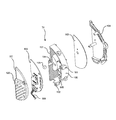
図4及び図5は、本発明の実施の形態の可動演出装置58の構成を説明する図である。
4 and 5 are diagrams illustrating the configuration of the
可動演出装置58は、第1演出ユニット63と第2演出ユニット64とを互いに離間し
た位置に備えて構成され、第1演出ユニット63及び第2演出ユニット64が連動して演
出動作が実行される。
The
図4は、可動演出装置58が動作する前の状態を示す図であり、図5は、可動演出装置
58が動作し、第1演出ユニット63及び第2演出ユニット64が動作した結果、当接部
(第1当接部121及び第2当接部122)にて当接している状態を示す図である。
FIG. 4 is a diagram illustrating a state before the
第1演出ユニット63は、センターケース51の左側、すなわち、基部ケース61の窓
部52の周縁の左側に配置される。また、第2演出ユニット64は、センターケース51
の右側に配置される。センターケース51の前方から見て第1演出ユニット63と第2演
出ユニット64との間に凹室62及び窓部52を臨ませるように配置される。
The
It is arranged on the right side. When viewed from the front of the
第1演出ユニット63は、表示部53aの前方へ移動可能な第1演出部材70と、該第
1演出部材70の駆動力を発生する第1演出駆動源としての役物駆動第1モータ(MOT
)71と、役物駆動第1MOT71から発生した駆動力(回動力)を第1演出部材70へ
伝達する第1演出伝達機構(第1主腕部材73及び第1副腕部材74)とを備える。
The
) 71 and a first effect transmission mechanism (a first
また、役物駆動第1MOT71の出力軸(第1出力軸)71aがセンターケース51の
前後方向に延在し、第1出力軸71aには第1駆動ギア76を共回り可能に軸着している
。
Further, an output shaft (first output shaft) 71a of the accessory driving
第1主腕部材73は、第1駆動ギア76と噛合される第1主腕ギア77が形成され、当
該第1駆動ギア76の上方に軸着される。第1副腕部材74は、第1駆動ギア76と噛合
される第1副腕ギア78が形成され、当該第1駆動ギア76の下方に軸着される。第1主
腕部材73及び第1副腕部材74は、基部ケース61と軸着された端部の反対側の端部が
互いに異なる位置で第1演出部材70に軸着し、第1演出部材70を支持している。
The first
第1演出ユニット63は、役物駆動第1MOT71を駆動して第1駆動ギア76をセン
ターケース51の正面から見て時計方向へ回動すると、役物駆動第1MOT71の駆動力
(回動力)を第1駆動ギア76及び第1主腕ギア77を介して第1主腕部材73へ伝達し
、この駆動力により第1主腕部材73がセンターケース51の正面から見て反時計方向へ
回動する。また、役物駆動第1MOT71の駆動力を第1駆動ギア76及び第1副腕ギア
78を介して第1副腕部材74へ伝達し、この駆動力により第1副腕部材74が第1主腕
部材73と同じ反時計方向へ回動する。この結果、第1演出部材70が第1主腕部材73
及び第1副腕部材74に支持された状態で上昇する。
When the
Ascending while being supported by the first
そして、役物駆動第1MOT71の駆動力により第1主腕部材73及び第1副腕部材7
4を上方へ延出して縦向き姿勢に設定すると、図4に示すように、第1演出部材70を表
示部53aの前方から外れて位置させた第1演出停止状態となり、第1演出部材70が窓
部52の側方に位置して、枠装飾部65の後方及び遊技盤本体10bの後方に隠れる(図
2参照)。
The first
When 4 is extended upward and set in the vertical orientation, as shown in FIG. 4, the
一方、第1演出停止状態から役物駆動第1MOT71を駆動して第1駆動ギア76をセ
ンターケース51の正面から見て反時計方向へ回動すると、役物駆動第1MOT71の駆
動力(回動力)を第1駆動ギア76及び第1主腕ギア77を介して第1主腕部材73へ伝
達し、この駆動力により第1主腕部材73がセンターケース51の正面から見て時計方向
へ回動する。
On the other hand, when the first
また、役物駆動第1MOT71の駆動力を第1駆動ギア76及び第1副腕ギア78を介
して第1副腕部材74へ伝達し、この駆動力により第1副腕部材74が第1主腕部材73
と同じ時計方向へ回動する。この結果、第1演出部材70が第1主腕部材73及び第1副
腕部材74に支持された状態で下降する。
The driving force of the accessory driving
Rotate in the same clockwise direction. As a result, the
そして、役物駆動第1MOT71の駆動力により第1主腕部材73及び第1副腕部材7
4を表示部53aの前方へ延出して横向き姿勢に設定すると、図5に示すように、第1演
出部材70を表示部53aの前方へ位置させた第1演出実行状態となり、第1演出部材7
0が表示部53aとカバーパネル部69との間の空間部のうち表示部53aの中央部分の
前方に位置する。
The first
When 4 is extended to the front of the
0 is located in front of the central portion of the
第2演出ユニット64は、表示部53aの前方へ移動可能な第2演出部材80と、該第
2演出部材80の駆動力を発生する第2演出駆動源としての役物駆動第2モータ(MOT
)81と、役物駆動第2MOT81から発生した駆動力(回動力)を第2演出部材80へ
伝達する第2演出伝達機構(第2主腕部材83及び第2副腕部材84)とを備える。
The
) 81 and a second effect transmission mechanism (second
また、役物駆動第2MOT81を出力軸(第2出力軸)81aがセンターケース51の
前後方向に延在し、第2出力軸81aには第2駆動ギア86を共回り可能に軸着している
。
Further, the accessory driving
第2主腕部材83は、第2駆動ギア86と噛合される第2主腕ギア87が形成され、当
該第2駆動ギア86よりも第1演出ユニット63寄りの位置に軸着される。第2副腕部材
84は、第2駆動ギア86と噛合される第2副腕ギア88が形成され、当該第2駆動ギア
86の下方に軸着される。第2主腕部材83及び第2副腕部材84は、基部ケース61と
軸着された端部の反対側の端部が互いに異なる位置で第2演出部材80に軸着し、第2演
出部材80を支持している。
The second
第2演出ユニット64は、役物駆動第2MOT81を駆動して第2駆動ギア86をセン
ターケース51の正面から見て時計方向へ回動すると、役物駆動第2MOT81の駆動力
(回動力)を第2駆動ギア86及び第2主腕ギア87を介して第2主腕部材83へ伝達し
、この駆動力により第2主腕部材83がセンターケース51の正面から見て反時計方向へ
回動する。また、役物駆動第2MOT81の駆動力を第2駆動ギア86及び第2副腕ギア
88を介して第2副腕部材84へ伝達し、この駆動力により第2副腕部材84が第2主腕
部材83と同じ反時計方向へ回動する。この結果、第2演出部材80が第2主腕部材83
及び第2副腕部材84に支持された状態で下降する。
When the
And descends while being supported by the second
そして、役物駆動第2MOT81の駆動力により第2主腕部材83及び第2副腕部材8
4を回動して第2演出部材80を下死点へ到達させ、引き続き第2主腕部材83及び第2
副腕部材84を回動して斜め下方へ延出して縦向き姿勢に設定し、第2演出部材80を下
死点から僅かに上昇させると、図4に示すように、第2演出部材80を表示部53aの前
方から外れて位置させた第2演出停止状態となり、第2演出部材80が枠装飾部65の後
方及び遊技盤本体10bの後方に隠れる(図2参照)。
The second
4 is rotated to bring the
When the
一方、第2演出停止状態から役物駆動第2MOT81を駆動して第2駆動ギア86をセ
ンターケース51の正面から見て反時計方向へ回動すると、役物駆動第2MOT81の駆
動力(回動力)を第2駆動ギア86及び第2主腕ギア87を介して第2主腕部材83へ伝
達し、この駆動力により第2主腕部材83がセンターケース51の正面から見て時計方向
へ回動する。
On the other hand, when the accessory driving
また、役物駆動第2MOT81の駆動力を第2駆動ギア86及び第2副腕ギア88を介
して第2副腕部材84へ伝達し、この駆動力により第2副腕部材84が第2主腕部材83
と同じ時計方向へ回動する。この結果、第2演出部材80が第2主腕部材83及び第2副
腕部材84に支持された状態で上昇する。
Further, the driving force of the accessory driving
Rotate in the same clockwise direction. As a result, the
そして、役物駆動第2MOT81の駆動力により第2主腕部材83及び第2副腕部材8
4を表示部53aの前方へ延出して横向き姿勢に設定すると、図5に示すように、第2演
出部材80を表示部53aの前方へ位置させた第2演出実行状態となり、第2演出部材8
0が表示部53aとカバーパネル部69との間の空間部のうち表示部53aの中央部分の
前方に位置する。
The second
When 4 is extended to the front of the
0 is located in front of the central portion of the
図6は、本発明の実施の形態の第1演出部材70の分解斜視図である。
FIG. 6 is an exploded perspective view of the
第1演出部材70は、センターケース51の正面から見て略半円形状の部材であり、第
1演出ユニット63側に円弧面を配置した姿勢に設定されている。
The
第1演出部材70には、基部となる第1演出ベース100が備えられる。第1演出ベー
ス100は、透明な樹脂によって形成される。第1演出ベース100の上部には、第1主
腕部材73を第1演出ベース100の前方から軸着する第1主腕軸着部101を形成し、
第1演出ベース100の下部には、第1副腕部材74を第1演出ベース100の後方から
軸着する第1副腕軸着部102を形成している。
The
A first sub-arm
第1演出ベース100の前面には、光を拡散しながら透過可能な第1光拡散シート10
3が重合される。さらに、第1光拡散シート103の前面に透明な第1保護パネル104
を重合することによって、第1光拡散シート103が第1演出部材70から脱落すること
を阻止している。
On the front surface of the first production base 100, a first
3 is polymerized. Further, a transparent first
The first
また、第1演出ベース100の後部を前方へ窪ませて第1基板収納空間部105を形成
し、該第1基板収納空間部105にLEDなどの発光装置(装飾装置620、図17参照
)が実装された第1発光基板106を収納する。さらに、この状態で第1基板収納空間部
105を第1ベース蓋部107で閉塞し、第1発光基板106が第1演出部材70から脱
落することを阻止している。
Further, the rear portion of the first production base 100 is recessed forward to form a first substrate
そして、第1発光基板106の発光装置から光を発生すると、この光が第1演出ベース
100、第1光拡散シート103、第1保護パネル104を透過してセンターケース51
の前方へ照射されるように構成されている。
Then, when light is generated from the light emitting device of the first light emitting substrate 106, this light is transmitted through the first effect base 100, the first
It is comprised so that it may irradiate ahead.
さらに、第1当接部121の第1基板収納空間部105側には、後部が開放された第1
演出磁石ホルダ124を窪ませて形成されている。第1演出磁石ホルダ124には、ボタ
ン形状の永久磁石からなる第1磁石125を磁極が第2演出部材80側へ向いた姿勢で、
第1磁石125が第1当接部121(第1演出磁石ホルダ124)から脱落しないように
収納されている。
Further, the
The
The
第1発光基板106には、装飾装置620の発光を制御するためのI2CI/Oエクス
パンダ615(図17参照)が搭載され、演出制御装置550から出力された制御信号(
電気信号)など送信するためのデータ線及びクロック線(信号線)が接続される。さらに
、装飾装置620を発光させるために必要な電力を供給するための電源線などが接続され
る。これらの接続線は、ケーブル108としてまとめられて接続されている。
The first light-emitting board 106 is equipped with an I 2 CI / O expander 615 (see FIG. 17) for controlling the light emission of the
A data line and a clock line (signal line) for transmission such as an electrical signal are connected. Further, a power line for supplying power necessary for causing the
図7は、本発明の実施の形態の第2演出部材80の分解斜視図である。
FIG. 7 is an exploded perspective view of the
第2演出部材80は、センターケース51の正面から見て上部に切欠部分がある略平行
四辺形状となっている。第2演出停止状態においては第2演出部材80の上下両側面を第
2演出ユニット64側から第1演出ユニット63側へ向けて下り傾斜させ(図4参照)、
第2演出実行状態においては当該第2演出部材80の左右両側面を第2演出ユニット64
側から第1演出ユニット63側へ向けて下り傾斜させる姿勢に設定されている(図5参照
)。
The
In the second effect execution state, the left and right side surfaces of the
The posture is set to be inclined downward from the side toward the
第2演出部材80には、基部となる第2演出ベース110が備えられる。第2演出ベー
ス110は、透明な樹脂によって形成される。第2演出ベース110の上部には、第2主
腕部材83を第2演出ベース110の前方から軸着する第2主腕軸着部111を形成し、
第2演出ベース110の下部には、第2副腕部材84を第2演出ベース110の後方から
軸着する第2副腕軸着部112を形成している。
The
A second sub-arm
さらに、第2演出ベース110の前面には、光を拡散しながら透過可能な第2光拡散シ
ート113を重合される。第2光拡散シート113の前面に透明な第2保護パネル114
を重合することによって、第2光拡散シート113が第2演出部材80から脱落すること
を阻止している。
Further, a second
The second
また、第2演出ベース110の後部を前方へ窪ませて第2基板収納空間部115を形成
し、該第2基板収納空間部115にLEDなどの発光装置(装飾装置620)が実装され
た第2発光基板116を収納し、この状態で第2基板収納空間部115を第2ベース蓋部
117で閉塞して、第2発光基板116が第2演出部材80から脱落することを阻止して
いる。
In addition, the rear portion of the
そして、第2発光基板116の発光装置から光を発生すると、この光が第2演出ベース
110、第2光拡散シート113、第2保護パネル114を透過してセンターケース51
の前方へ照射されるように構成されている。
When light is generated from the light emitting device of the second
It is comprised so that it may irradiate ahead.
さらに、第2当接部122の第2基板収納空間部115側には、後部が開放された第2
演出磁石ホルダ128を窪ませて形成されている。第2演出磁石ホルダ128には、ボタ
ン形状の永久磁石からなる第2磁石129が、第1当接部121及び第2当接部122を
挟んで第1磁石125とは対称となる位置に収納されている。
Further, the
The
第2発光基板116には、第1発光基板106と同様に、装飾装置620の発光を制御
するためのI2CI/Oエクスパンダ615(図17参照)が搭載され、演出制御装置5
50から出力された制御信号などを送信するためのデータ線及びクロック線(信号線)が
接続される。さらに、装飾装置620を発光させるために必要な電力を供給するための電
源線などが接続される。これらの接続線は、ケーブル118としてまとめられて接続され
ている。
Similarly to the first light-emitting substrate 106, the second light-emitting
A data line and a clock line (signal line) for transmitting a control signal output from 50 are connected. Further, a power line for supplying power necessary for causing the
可動演出装置58は、第1演出部材70に第1当接部121を備えるとともに、第2演
出部材80に第2当接部122を備える。そして、第1演出ユニット63を第1演出実行
状態へ変換するとともに、第2演出ユニット64を第2演出実行状態へ変換すると、第1
当接部121と第2当接部122とが当接し、第1演出部材70と第2演出部材80とで
1つの装飾体を形成する。このとき、第1磁石125と第2磁石129との間で吸引力を
発生するように第1磁石125及び第2磁石129が配置されている。さらに、この形成
された装飾体を表示部53aの中央部の前方に位置させるように構成している。
The
The
図8は、本発明の実施の形態の遊技機1の配線を説明する図である。
FIG. 8 is a diagram illustrating wiring of the
図8では、遊技盤本体10bにセンターケース51が取り付けられ、表示装置53がセ
ンターケース51に取り付けられる前の状態を示している。また、表示装置53の背面に
は、演出制御装置550が取り付けられている。演出制御装置550には、接続端子90
が備えられており、接続端子90を介して制御対象の演出装置に対し、制御信号の送信や
電力の供給を行う。具体的には、後述する中継基板600にケーブル91を介して接続す
る。
FIG. 8 shows a state before the
Are provided, and control signals are transmitted and electric power is supplied to the rendering device to be controlled via the
また、遊技盤本体10bの背面下部には、遊技制御装置500や各種制御基板を含む制
御ユニット700が配置される。制御ユニット700に搭載される制御基板には、演出制
御装置550から送信された制御信号を、装飾制御装置610(図11参照)に中継する
中継基板600が含まれる。装飾制御装置610は、詳細については後述するが、遊技を
演出するための発光装置(例えば、LED)や可動物(例えば、モータ)などの演出装置
の制御を行う。また、中継基板600は、装飾制御装置610と同様に、発光装置や可動
物を接続可能である。
In addition, a
中継基板600には、演出制御装置550にケーブル91を介して接続される上流コネ
クタ601が備えられる。ケーブル91の一方のコネクタ91aは、前述のように、演出
制御装置550の接続端子90に接続される。ケーブル91の他方のコネクタ91bは、
中継基板600の上流コネクタ601に接続される。さらに、遊技機1に備えられた各演
出装置の制御を行う装飾制御装置610に接続するためのコネクタ602a〜602eを
備える。
The
It is connected to the
さらに、中継基板600には、接続されたケーブルの接続状態を示す空き端子モニタ6
03が備えられている。空き端子モニタ603の詳細については、図15にて説明する。
Further, the
03 is provided. Details of the empty
また、図示は略するが、遊技制御装置500を構成するユニットが、中継基板600の
コネクタ装着面を覆うようにして設けられている。そのため、遊技制御装置500は、中
継基板600の各コネクタに必要なケーブルを装着した後に取り付けられる配置構成とな
っている。
Although illustration is omitted, units constituting the
前面枠3には、当該前面枠3に配置されたスピーカ30及び装飾部材9a、9bなどを
制御するための信号を送信するケーブル3bが接続されている。このケーブル3bのコネ
クタは、演出制御装置550の接続端子92に接続される。
Connected to the
遊技盤本体10bには、サイドランプ45を取り付けるための開口部45bが形成され
ている。サイドランプ45には、電力及び信号を送信するケーブル45aが接続され、開
口部45bから遊技盤10の裏面側へ導入される。遊技盤10の裏面側へ導入されたケー
ブル45aは、中継基板600に接続され、例えば、コネクタ602dに接続される。
An
また、遊技盤10の下部には、図2に示したように、始動口36及び大入賞口42が配
置される。始動口36が配置されている遊技盤10の裏側には、普図変動表示ゲームに当
選した場合に開放される開閉部材36aを開閉するための普電ソレノイド(SOL)36
bが配置される。また、特図変動表示ゲームに当選した場合に、大入賞口42を開閉する
ための大入賞口SOL42bも遊技盤10の裏側に配置されている。普電SOL36b及
び大入賞口SOL42bには、制御信号の入力を受け付けるためのケーブル(図示略)が
接続され、このケーブルは遊技制御装置500に接続されている。また、ケーブル42C
は、大入賞口42の内部に備えられる演出用のLEDを点灯させるための電力及び信号を
伝達するケーブルとして中継基板600に接続され、例えば、コネクタ602fに接続さ
れる。
Further, as shown in FIG. 2, a starting
b is arranged. In addition, a special winning
Is connected to the
前述のように、遊技盤10の中央部には、センターケース51が取り付けられている。
センターケース51の内部には、第1演出部材70及び第2演出部材80によって構成さ
れる可動演出装置58が備えられる。図8では、第1演出部材70及び第2演出部材80
が当接面(121,122)で当接している状態となっている。
As described above, the
Inside the
Is in contact with the contact surfaces (121, 122).
また、可動演出装置58の第1演出ユニット63及び第2演出ユニット64には、前述
のように、第1演出部材70及び第2演出部材80を稼動させるためのモータ(役物駆動
第1モータ71、役物駆動第2モータ81)が備えられている。そして、これらのモータ
を制御するための信号及びモータを駆動させるための電力を供給するためのケーブル65
2が可動演出装置58に接続されている。また、可動演出装置58には、これらのモータ
の動作状態を検知するためのモータ位置検出センサ(図示せず)が備えられており、セン
シング結果を受信するためのケーブル651が接続されている。ケーブル652及びケー
ブル651は、センターケース51の開口部51bから遊技盤10の裏面側に延びており
、中継基板600に接続される。例えば、ケーブル652はコネクタ602Cに接続され
、ケーブル651はコネクタ602eに接続される。
Further, as described above, the
2 is connected to the
さらに、演出制御装置550から出力された制御信号を、センターケース51の内部に
配置されたLEDなどの演出装置を制御するための装飾制御装置610(図11参照)へ
伝達するケーブル653が接続される。ケーブル653は、センターケース51に設けら
れた開口部51aから遊技盤10の裏面側の中継基板600に接続され、例えば、コネク
タ602aに接続される。
Furthermore, a
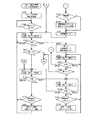
図9は、本発明の実施の形態の遊技機1の構成を示すブロック図である。
FIG. 9 is a block diagram showing a configuration of the
遊技機1は、遊技を統括的に制御する遊技制御装置500、各種演出を行うために表示
装置53及びスピーカ30等を制御する演出制御装置550、遊技球を払い出すために図
示しない払出モータを制御する払出制御装置580を備える。
The
まず、遊技制御装置500の構成について説明する。なお、演出制御装置550につい
ては、図10にて説明する。
First, the configuration of the
遊技制御装置500は、遊技用マイコン501、入力I/F(Interface)5
05、出力I/F(Interface)506、及び外部通信端子507を備える。
The
05, an output I / F (Interface) 506, and an
遊技用マイコン501は、CPU502、ROM(Read Only Memory)
503及びRAM(Random Access Memory)504を備える。
The
503 and RAM (Random Access Memory) 504.
CPU502は、遊技を統括的に制御する主制御装置であって、遊技制御を司る。RO
M503は、遊技制御のための不変の情報(プログラム、データ等)を記憶している。R
AM504は、遊技制御時にワークエリアとして利用される。
The CPU 502 is a main control device that controls the game in an integrated manner, and controls the game. RO
M503 stores invariant information (program, data, etc.) for game control. R
The
外部通信端子507は、遊技制御装置500の設定情報等を検査する検査装置等の外部
機器に遊技制御装置500を接続する。
The
CPU502は、入力I/F505を介して各種入力装置(始動口SW36d、一般入
賞口SW44a〜44n、ゲートSW34a、カウントSW42d、ガラス枠開放SW1
8a、前面枠開放SW3a、球切れSW54、振動センサ55、及び磁気センサ56)か
らの検出信号を受けて、大当り抽選等、種々の処理を行う。
The CPU 502 receives various input devices (start opening SW36d, general winning openings SW44a to 44n, gate SW34a, count SW42d, glass frame opening SW1 via the input I /
8a, the front
始動口SW36dは、始動口36に遊技球が入賞したことを検出するスイッチである。
一般入賞口SW44a〜44nは、一般入賞口44に遊技球が入賞したことを検出するス
イッチである。
The start port SW36d is a switch that detects that a game ball has won the
The general winning
ゲートSW34aは、普図始動ゲート34を遊技球が通過したことを検出するスイッチ
である。カウントSW42dは、大入賞口42に遊技球が入賞したことを検出するスイッ
チである。
The
ガラス枠開放SW18aは、ガラス枠18が開放されたことを検出するスイッチである
。前面枠開放SW3aは、前面枠3が開放されたことを検出するスイッチである。
The glass
球切れSW54は、遊技機1の内部に貯留され、払い出しに用いられる遊技球の数が所
定数以下になったことを検出するスイッチである。
The ball cut
振動センサ55は、遊技機1に与えられた振動を検出するセンサであり、遊技機1を振
動させるなどの不正行為を検出する。磁気センサ56は、始動口36の第2始動入賞口、
一般入賞口44、大入賞口42、及び普図始動ゲート34付近に設けられ、磁力を検出す
るセンサである。磁気センサ56は、各入賞口付近に磁石を近づけて、遊技領域10aに
発射された遊技球を各入賞口に導く不正を検出する。
The
It is a sensor that is provided in the vicinity of the general winning
また、CPU502は、出力I/F506を介して、普図・特図表示器35、普電SO
L36b、大入賞口SOL42b、払出制御装置580、及び演出制御装置550に指令
信号を送信して、遊技を統括的に制御する。
In addition, the CPU 502 is connected to the ordinary / special-
A command signal is transmitted to L36b, special winning opening SOL42b,
普図・特図表示器35には、前述のように、特図変動表示ゲーム及び普図変動表示ゲー
ムが実行される。さらに、特図変動表示ゲームの未処理回数(特図始動記憶数)及び普図
変動表示ゲームの未処理回数(普図始動記憶数)が表示される。普図変動表示ゲームが当
りとなるか否かを示す乱数を含む普図始動記憶、及び特図変動表示ゲームが当りとなるか
否かを示す乱数を含む特図始動記憶が記憶されている。
As described above, the special figure change display game and the universal figure change display game are executed on the special figure / special
普電SOL36bは、普図変動表示ゲームの停止表示が特別の結果態様となった場合に
、開閉部材36aを開放することによって、始動口36に遊技球が入賞しやすい状態にす
る。
The general
大入賞口SOL42bは、特図変動表示ゲームの結果が特別の結果態様となって、特別
遊技状態(大当たり状態)となった場合に、大入賞口42の開閉扉42aを開放して、遊
技球が入賞しやすい状態に変換する。
The special winning opening SOL42b opens the open /
遊技制御装置500は、外部情報端子508から図示しない情報収集端末装置を介して
、遊技機データを図示しない遊技場管理装置に出力する。遊技場管理装置は、遊技場に設
置された遊技機1の遊技データを収集管理する計算機である。
The
払出制御装置580は、遊技球が一般入賞口44又は大入賞口42に入賞した場合に、
入賞した入賞口に対応する数の遊技球の払出指令を遊技制御装置500から受信する。ま
た、球貸ボタン26が操作された場合にも所定数の遊技球の払い出しを行う払出指令を遊
技制御装置500から受信する。払出制御装置580は、受信した払出指令に基づいて、
図示しない払出モータを制御し、払出指令に指定された数の遊技球を払い出す。
The
A payout command for the number of game balls corresponding to the winning winning award is received from the
A payout motor (not shown) is controlled to pay out the number of game balls specified in the payout command.
遊技制御装置500は、変動開始コマンド、客待ちデモコマンド、ファンファーレコマ
ンド、確率情報コマンド、及びエラー指定コマンド等を、遊技の状況を示す遊技データと
して、出力I/F506を介して、演出制御装置550へ送信する。
The
図10は、本発明の実施の形態の演出制御装置550の構成を示すブロック図である。
FIG. 10 is a block diagram showing a configuration of the
演出制御装置550は、遊技制御装置500から入力される遊技データに基づいて、演
出内容を決定し、表示装置53を制御するとともに、遊技盤10及び前面枠3に備えられ
た各種演出装置を制御する。演出装置には、LEDなどの発光装置やモータ又はソレノイ
ドなどの可動物が含まれる。
The
演出制御装置550は、CPU551、制御ROM552、RAM553、画像ROM
554、音ROM555、VDP556、音LSI557、入力I/F558b、出力I
/F558a、電源投入検出回路559、第1マスタIC570a、第2マスタIC57
0b、NORゲート回路561及び監視タイマ回路562を備える。さらに、演出制御装
置550は、遊技盤10に接続される接続端子90と、前面枠3に接続される接続端子9
2を備える。なお、第1マスタIC570a及び第2マスタIC570bに共通の機能に
ついては、単に「マスタIC」として説明する。
The
554,
/ F558a, power-on
0b, a NOR
2 is provided. The functions common to the
CPU551は、遊技制御装置500から送信された指令信号が通信割込としての割込
信号(INT)として入力され、入力された指令信号に基づいて、各種演出を制御する。
また、CPU551には、第1マスタIC570a及び第2マスタIC570bからマス
タ割込としての割込信号(INT)が入力されるとともに、VDP556からも画像更新
割込としての割込信号(INT)が入力される。
The
The
さらに、CPU551は、監視タイマ回路562からもタイムアウト割込としての割込
信号(INT)が入力される。監視タイマ回路562は、複数種類の監視タイマが内蔵さ
れており、CPU551によって設定された監視タイマ値がタイムアップすると、CPU
551に割込信号を出力する。CPU551は、割込信号の入力を受け付けると、実行中
の処理を中断し、入力された割込信号に対応する処理を実行する。
Further, the
An interrupt signal is output to 551. When the
制御ROM552には、演出制御のための不変の情報(プログラム、データ等)が格納
されている。RAM553は、演出制御時にワークエリアとして利用される。
The
画像ROM554は、VDP556に接続され、表示装置53に表示される画像データ
を格納する。VDP556は、表示装置53への画像出力を制御するプロセッサである。
The
また、VDP556は、表示装置53に表示される画像を更新する周期(33ms周期
)と同期する同期信号を発生させる同期信号発生手段を備える。同期信号発生手段は、同
期信号を発生させるごとに、発生させた同期信号をCPU551に割込信号として入力す
る。
In addition, the
音ROM555は、音LSI557に接続され、前面枠3に備えられたスピーカ30か
ら出力される音データを格納する。音LSI557は、スピーカ30からの音声出力を制
御する回路である。
The
入力I/F558bは、フィルタ565a及び565bを介して外部から入力された情
報を受け付けるインタフェースである。具体的には、前面枠3に備えられた演出ボタン1
7が操作されたことを示す信号の入力を受け付けたり、遊技盤10に備えられたモータ位
置検出センサによって検出された各モータの位置情報などの入力を受け付けたりする。
The input I /
7 is received, or an input of position information of each motor detected by a motor position detection sensor provided in the
電源投入検出回路559は、演出制御装置550に電源が投入された場合に、第1マス
タIC570a及び第2マスタIC570bのレジスタをデフォルト状態(すべて0)に
初期化するリセット信号を発生させ、NORゲート回路561に出力する。
The power-on
また、CPU551は、所定の条件が成立した場合に、バス563を介してリセット信
号を出力I/F558aに出力する。そして、出力I/F558aは、入力されたリセッ
ト信号をNORゲート回路561に出力し、さらに、NORゲート回路561から、第1
マスタIC570a及び第2マスタIC570bに当該リセット信号を出力する。所定の
条件とは、例えば、すべての装飾制御装置610において、エラーフラグが「ON」にな
った場合などである(図32及び図33参照)。
Further, the
The reset signal is output to the
また、出力I/F558aは、ドライバ564a及びドライバ564bを介して、遊技
盤10や前面枠3に備えられた演出装置(モータ又はソレノイドなどの可動物で駆動する
演出装置)へ制御信号を出力する。
Further, the output I /
なお、電源投入検出回路559からNORゲート回路561に入力されるリセット信号
と、CPU551から出力I/F558aを介してNORゲート回路561に入力される
リセット信号は、いずれの場合にもLOWレベルの状態のときにリセットを指令する信号
として機能する。そのため、電源投入検出回路559及びCPU551の少なくとも一方
からNORゲート回路561にリセット信号が出力されていれば、NORゲート回路56
1を介してリセット信号が第1マスタIC570a及び第2マスタIC570bに入力さ
れる。
Note that the reset signal input from the power-on
1 is input to the
図11は、本発明の実施の形態の演出制御装置550に備えられた第1マスタIC57
0aと遊技盤10に備えられた演出装置の構成を示すブロック図である。
FIG. 11 shows the
FIG. 3 is a block diagram illustrating a configuration of a rendering device provided in 0a and the
遊技盤10は、第1マスタIC570aに接続される中継基板600、当該中継基板6
00に接続される装飾装置基板625及び補助遊技装置ユニット12を備える。
The
The
中継基板600は、第1マスタIC570aから送信された電気信号を、遊技盤10に
備えられた装飾制御装置610に送信(中継)する。また、中継基板600には、装飾制
御装置610と同様に、演出装置を制御する機能を有し、当該中継基板600に直接接続
された装飾装置基板625を制御する。
The
装飾装置620は、装飾制御装置610に備えられるI2CI/Oエクスパンダ615
(図17参照)によって制御され、電流を流すことによって光が点滅して演出を行う発光
装置であり、例えばLEDなどである。装飾装置基板625は、サイドランプ45(図8
参照)に設けられる基板であり、サイドランプ45の発光装置(LED)が搭載されてい
る。このサイドランプ45の発光装置は、中継基板600に備えられるI2CI/Oエク
スパンダ615によって、直接制御される。
The
(Refer to FIG. 17) is a light-emitting device that produces an effect by flashing light by passing an electric current, such as an LED. The
The light emitting device (LED) of the
補助遊技装置ユニット12には、LEDなどの発光装置である装飾装置620、可動物
である役物駆動第1モータ(MOT)71及び役物駆動第2MOT81が含まれている。
補助遊技装置ユニット12内の装飾装置620は、当該補助遊技装置ユニット12に含ま
れる装飾制御装置610によって制御される。本発明の実施の形態では、役物駆動第1M
OT71及び役物駆動第2MOT81は、中継基板600によって制御されるように構成
されているが、装飾装置620と同様に当該補助遊技装置ユニット12に含まれる装飾制
御装置610によって制御されるように構成してもよい。
The auxiliary
The
The
役物駆動第1MOT71及び役物駆動第2MOT81は、電流が流れると回転動作する
ことによって演出動作を行う駆動装置である。役物駆動第1MOT71及び役物駆動第2
MOT81は、演出制御装置550のドライバ564により中継基板600を経由して直
接制御されるので、I2CI/Oエクスパンダ615を介在させる処理は行われない。
The first
Since the
本発明の実施の形態では、役物駆動第1MOT71及び役物駆動第2MOT81は、可
動演出装置58に含まれ、具体的には、役物駆動第1MOT71は第1演出ユニット63
、役物駆動第2MOT81は第2演出ユニット64に含まれている。
In the embodiment of the present invention, the accessory driving
The accessory driving
演出制御装置550は、役物駆動第1MOT71及び役物駆動第2MOT81を制御す
ることによって、第1演出ユニット63及び第2演出ユニット64が連動した演出動作を
実行させる。
The
第1マスタIC570aは、制御対象となる装飾装置620を制御する装飾制御装置6
10に個別に割り当てられたアドレスを指定して、指定した個別アドレスの装飾制御装置
610に装飾装置620の制御内容を出力する。なお、装飾制御装置610の個別アドレ
スは、正確には、装飾制御装置610に含まれるI2CI/Oエクスパンダ615(図1
7参照)の個別アドレスである。
The
The address individually assigned to 10 is designated, and the control content of the
7).
第1マスタIC570aは、接続線SDA、接続線SCL、接続線GND、接続線Vc
c、接続線Vled、接続線Vms、及び接続線Vseの7種類の接続線を介して、中継
基板(装飾制御装置)600に接続される。これらの接続線は、第1マスタIC570a
と中継基板600とを接続するケーブル91(図8参照)により構成される。
The
c, the connection line Vled, the connection line Vms, and the connection line Vse are connected to the relay board (decoration control device) 600 through seven types of connection lines. These connection lines are connected to the
And the
接続線SDAは、演出制御装置550と装飾制御装置610との間でデータを通信する
ための接続線であり、本発明の実施の形態におけるデータ線として機能する。接続線SC
Lは、接続線SDAでのデータ通信に用いられるクロック信号を入出力するための接続線
であり、本発明の実施の形態におけるタイミング信号線として機能する。接続線GNDは
、接続線Vcc、接続線Vled、接続線Vms、及び接続線Vseで供給される電源の
グランドである。
Connection line SDA is a connection line for communicating data between
L is a connection line for inputting and outputting a clock signal used for data communication on the connection line SDA, and functions as a timing signal line in the embodiment of the present invention. The connection line GND is a ground of the power supplied by the connection line Vcc, the connection line Vled, the connection line Vms, and the connection line Vse.
接続線Vccは、中継基板600及び装飾制御装置610にロジック用の電源を供給す
るための接続線である。接続線Vledは、LED(装飾装置620)を発光させるため
の電源を供給するための接続線である。接続線Vmsは、補助遊技装置ユニット12に含
まれるモータやソレノイド(具体的には、役物駆動第1MOT71、役物駆動第2MOT
81)に電源を供給するための接続線である。接続線Vseは、各種センサ(演出装置に
含まれるモータの状態を検出する状態検出センサであって、具体的には、モータ位置検出
センサ560aが相当する)に電源を供給するための接続線である。
The connection line Vcc is a connection line for supplying logic power to the
81) is a connection line for supplying power. The connection line Vse is a connection line for supplying power to various sensors (a state detection sensor that detects the state of the motor included in the rendering device, and specifically corresponds to the motor
中継基板600と補助遊技装置ユニット12との間は、演出制御装置550と中継基板
600との間を接続する7種類の接続線が接続される。本発明の実施の形態では、モータ
位置検出センサ560a、役物駆動第1MOT71及び役物駆動第2MOT81は、中継
基板600によって直接制御されるため、前述した7種類の接続線のうち、接続線Vms
及び接続線Vse以外の5種類の接続線が、補助遊技装置ユニット12の最上流に配置さ
れた装飾制御装置610に接続される。具体的には、中継基板600と装飾制御装置61
0との間は、接続線Vcc、接続線Vled、接続線SDA、接続線SCL及び接続線G
NDが接続される。
Between the
The five types of connection lines other than the connection line Vse are connected to the
Between 0, the connection line Vcc, the connection line Vled, the connection line SDA, the connection line SCL, and the connection line G
ND is connected.
なお、図8に示した配線(ケーブル)と各接続線を対応させると、演出制御装置550
から中継基板600に引き渡される各種接続線(接続線Vcc、接続線Vled、接続線
SDA、接続線SCL、接続線Vms、接続線Vse、及び接続線GND)は、ケーブル
91に含まれている。
When the wiring (cable) shown in FIG. 8 is associated with each connection line, the
Various connection lines (connection line Vcc, connection line Vled, connection line SDA, connection line SCL, connection line Vms, connection line Vse, and connection line GND) delivered to the
また、これらの各種接続線は、中継基板600からさらに分岐して別の基板に引き渡さ
れ、中継基板600から分岐する接続線Vcc、接続線Vled、接続線SDA、及び接
続線SCLはケーブル653に、接続線Vmsはケーブル652に、接続線Vseはケー
ブル651に含まれている。また、中継基板600から分岐する接続線GNDが、ケーブ
ル651〜653の全てに含まれている。
These various connection lines are further branched from the
第1マスタIC570aと装飾制御装置610とは、接続線SDA及び接続SCLによ
って2ライン双方向通信を行う。第1マスタIC570aは、CPU551からの指令に
基づいて、装飾制御装置610との間に接続された接続線SDA及び接続線SCLの各信
号レベルを制御する(第1の)信号レベル制御手段として機能する。
The
第1マスタIC570aは、中継基板600及び装飾制御装置610にデータを送信す
る場合には、まず、接続線SCLの信号レベルをHIGHに維持したまま、接続線SDA
の信号レベルをHIGHからLOWに変化させることにより、装飾制御装置610へのデ
ータ出力を開始するためのスタート条件を成立させる(装飾制御装置610に対してスタ
ートコンディションを発行(出力)する)。
When transmitting data to the
Is changed from HIGH to LOW to establish a start condition for starting data output to the decoration control device 610 (issue (output) a start condition to the decoration control device 610).
この後、第1マスタIC570aは、接続線SCLの信号レベルをLOWに変更し、接
続線SCLの信号レベルがLOWである間に接続線SDAの信号レベルを送信データの最
初のビットのレベルに設定し、所定時間後に接続線SCLの信号レベルをLOWからHI
GHに変化させる。接続線SCLの信号レベルがHIGHに変化すると、装飾制御装置6
10は接続線SDAの信号レベルを取得し、送信データの最初のビットとして認識する。
次いで、第1マスタIC570aは、接続線SCLの信号レベルをHIGHからLOWに
戻す。
Thereafter, the
Change to GH. When the signal level of the connection line SCL changes to HIGH, the
10 acquires the signal level of the connection line SDA and recognizes it as the first bit of the transmission data.
Next, the
この手順を1回実行すると、第1マスタIC570aから装飾制御装置610へ1ビッ
トのデータが送信され、最終的にはこの手順が8回繰り返されることで、送信データの8
ビットすべてが第1マスタIC570aから装飾制御装置610へ送信される(1バイト
分のデータが送信される)。
When this procedure is executed once, 1-bit data is transmitted from the
All the bits are transmitted from the
そして、第1マスタIC570aは、最後の8ビット目のデータ送信が終了すると、接
続線SCLの信号レベルをHIGHからLOWに戻した際に、接続線SDAを解放して装
飾制御装置610からの返答信号を受信することを待機する受信待機状態にする。
Then, when the data transmission of the last 8 bits is completed, the
受信待機状態になると、装飾制御装置610は、接続線SDAを介して1ビットの返答
信号(後述するACK又はNACK)を第1マスタIC570aに返す。次いで、第1マ
スタIC570aは、接続線SCLの信号レベルをLOWからHIGHに変化させて返答
信号のレベルを取り込み、所定時間後に接続線SCLの信号レベルをHIGHからLOW
に変化させると、装飾制御装置610は接続線SDAを解放する。
In the reception standby state, the
The
第1マスタIC570aは、このような1バイト分のデータ送信(下り方向データの送
信)と1ビット分の返答信号の受信(上り方向データの受信)とを交互に繰り返し、装飾
制御装置610へ出力すべきデータがすべて出力されるまで継続する。第1マスタIC5
70aは、出力すべきデータの出力が終了した場合には、接続線SCLの信号レベルをH
IGHに維持したまま、接続線SDAの信号レベルをLOWからHIGHに変更させるこ
とにより、装飾制御装置610へのデータ出力を終了するためのストップ条件を成立させ
る(装飾制御装置610に対してストップコンディションを発行する)。
The
70a sets the signal level of the connection line SCL to H when the output of the data to be output is completed.
The stop condition for terminating the data output to the
入力用バッファ571は、装飾制御装置610から接続線SDAを介して入力されたデ
ータが一時的に記憶される記憶装置である。
The
具体的には、第1マスタIC570aが入力モードに設定された場合において、装飾制
御装置610から第1マスタIC570aに送信されたデータが、フィルタ575aによ
りノイズが除去されて入力用バッファ571に一時的に記憶される。
Specifically, when the
出力用バッファ572は、装飾制御装置610に接続線SDAを介して出力するデータ
が一時的に記憶される。
The
リセットレジスタ(REG)573は、バス563に接続され、演出制御装置550の
CPU551からの指令を受け付けてリセット信号をコントローラ574に出力する。コ
ントローラ574は、第1マスタIC570aを統括的に制御し、各種処理を実行する。
The reset register (REG) 573 is connected to the
フィルタ575aは、接続線SDAから入力されたデータのノイズを除去する。ドライ
バ576aは、接続線SDAからデータを出力する場合に、トランジスタ578aが動作
可能な電圧をトランジスタ578aに印加する。
The
接続線SDAは、プルアップ抵抗Rによって所定の電圧が印加され(図21参照)、フ
ィルタ575a及びトランジスタ578aに接続されている。
A predetermined voltage is applied to the connection line SDA by a pull-up resistor R (see FIG. 21), and the connection line SDA is connected to the
トランジスタ578aは、電力消費を抑えるために電界効果トランジスタ(FET)が
用いられている。トランジスタ578aのゲートはドライバ576aに接続され、ドレイ
ンはプルアップ抵抗Rにより所定の電圧が印加された接続線SDAに接続され、ソースは
接地されている。
As the
トランジスタ578aのゲートに印加される電圧がトランジスタ578aを動作させる
所定値よりも小さければ、ドレインとソースとの間に電流が流れないので、接続線SDA
に印加された電圧は降下せず、その結果、接続線SDAはHIGHレベルとなる。一方、
トランジスタ578aのゲートに印加される電圧がトランジスタ578aを動作させる所
定値以上であれば、所定値の電圧が印加されたドレインから接地されているソースへ電流
が流れることによって、接続線SDAの電圧が低下し、その結果、接続線SDAはLOW
レベルとなる。
If the voltage applied to the gate of the
As a result, the connection line SDA becomes HIGH level. on the other hand,
When the voltage applied to the gate of the
Become a level.
なお、トランジスタ578aは、10ミリアンペア程度の電流をドレインからソースへ
流しても破損しない仕様のものを用いている。このため、接続線SDAには、通常のI2
Cバス使用で用いられる電流値よりもはるかに大きい10ミリアンペア程度の電流を流す
ことが可能であり、演出制御装置550と装飾制御装置610との間のデータ送信が、ノ
イズによる障害に耐えうる構成となっている。
Note that the
It is possible to pass a current of about 10 milliamperes that is much larger than the current value used when using the C bus, and the data transmission between the
ドライバ576aは、データを接続線SDAから出力する場合に、トランジスタ578
aにドレインとソースとの間に電流を流すためにトランジスタ578aのゲートにトラン
ジスタ578aが動作可能な値の電圧を印加する。そして、ドライバ576aは、接続線
SDAの電圧を、HIGHレベル又はLOWレベルに設定することによって、データを接
続線SDAから出力する。
When the
In order to pass a current between the drain and source in a, a voltage having a value that allows the
また、フィルタ575bは、接続線SCLから入力されたデータのノイズを除去する。
ドライバ576bは、接続線SCLからデータを出力する場合に、トランジスタ578b
が動作可能な電圧をトランジスタ578bに印加する。
Further, the
When the
Is applied to the
接続線SCLは、プルアップ抵抗Rによって所定の電圧が印加され(図21参照)、フ
ィルタ575b及びトランジスタ578bに接続されている。
A predetermined voltage is applied to the connection line SCL by the pull-up resistor R (see FIG. 21), and the connection line SCL is connected to the
トランジスタ578bは、電力消費を抑えるために電界効果トランジスタ(FET)が
用いられている。トランジスタ578bのゲートはドライバ576bに接続され、ドレイ
ンはプルアップ抵抗Rにより所定の電圧が印加された接続線SCLに接続され、ソースは
接地されている。
A field effect transistor (FET) is used as the
トランジスタ578bのゲートに印加される電圧がトランジスタ578bを動作させる
所定値よりも小さければ、ドレインとソースとの間に電流が流れないので、接続線SCL
に印加された電圧は降下せず、その結果、接続線SCLはHIGHレベルとなる。一方、
トランジスタ578bのゲートに印加される電圧がトランジスタ578bを動作させる所
定値以上であれば、所定値の電圧が印加されたドレインから接地されているソースへ電流
が流れることによって、接続線SCLの電圧が低下し、その結果、接続線SCLはLOW
レベルとなる。
If the voltage applied to the gate of the
As a result, the connection line SCL becomes HIGH level. on the other hand,
If the voltage applied to the gate of the
Become a level.
なお、トランジスタ578bは、10ミリアンペア程度の電流をドレインからソースへ
流しても破損しない仕様のものを用いている。そのため、接続線SCLには、通常のI2
Cバス使用で用いられる電流値よりもはるかに大きい10ミリアンペア程度の電流を流す
ことが可能であり、演出制御装置550と装飾制御装置610との間のデータ送信が、ノ
イズによる障害に耐えうる構成となっている。
Note that the
It is possible to pass a current of about 10 milliamperes that is much larger than the current value used when using the C bus, and the data transmission between the
ドライバ576bは、クロック信号を接続線SCLから出力する場合に、トランジスタ
578bにドレインとソースとの間に電流を流すためにトランジスタ578bのゲートに
トランジスタ578bが動作可能な値の電圧を印加する。そして、ドライバ576bは、
接続線SCLの電圧を、HIGHレベルとLOWレベルとに繰り返し変化させることによ
って、クロック信号を接続線SCLから出力する。
When the
A clock signal is output from the connection line SCL by repeatedly changing the voltage of the connection line SCL between a HIGH level and a LOW level.
電源投入リセット回路577は、第1マスタIC570aに電源が投入されて、電源投
入リセット回路577内の電圧が所定値に達した場合に、入力用バッファ571及び出力
用バッファ572などの記憶領域をデフォルト状態にするためのリセット信号をコントロ
ーラ574に出力する。なお、電源投入リセット回路577については、第1マスタIC
570aの外部に設け、後述する第2マスタIC570bの共通としてもよい。
The power-on
It may be provided outside 570a and may be common to a
コマンドレジスタ(REG)581は、演出制御装置550のCPU551からコマン
ドを受け付けるためのレジスタである。本発明の実施の形態では、コマンドレジスタ58
1には、STA、STO、SI、及びMODEの各ビットが予め割り当てられており、C
PU551によって、各ビット毎個別に"0"又は"1"が設定可能となっている。
The command register (REG) 581 is a register for receiving a command from the
1, each bit of STA, STO, SI, and MODE is assigned in advance, and C
With the
STAは、第1マスタIC570aが制御対象の装飾制御装置610に対し、スタート
条件(スタートコンディション)の出力を指示するためのビットである。STAに"1"が
設定されると、第1マスタIC570aは、制御対象の装飾制御装置610に対し、スタ
ートコンディションを発行(出力)し、スタート条件を成立させる。
The STA is a bit for the
STOは、第1マスタIC570aが制御対象の装飾制御装置610に対し、ストップ
条件(ストップコンディション)の出力を指示するためのビットである。STOに"1"が
設定されると、第1マスタIC570aは、制御対象の装飾制御装置610に対し、スト
ップコンディションを発行(出力)し、ストップ条件を成立させる。
The STO is a bit for the
SIは、第1マスタIC570aから、演出制御装置550において割込みを発生させ
るときに設定されるビットである。第1マスタIC570aからCPU551に割込みを
発生させるときには、コントローラ574によってSIに"1"が設定され、割込信号(I
NT)がCPU551に入力される。その後、SIに"1"が設定されている間は、第1マ
スタIC570aは処理を中断しているが、CPU551によってSIに"0"が設定され
ると、第1マスタIC570aは、割込を中断して処理を再開する。
SI is a bit that is set when an interrupt is generated in the
NT) is input to the
MODEは、データを送信するモードを指定するビットであり、"1"が設定されている
場合には「バッファモード」、"0"が設定されている場合には「バイトモード」が指定さ
れる。バッファモードは、連続する複数バイトのデータを1度にまとめて送信するモード
であり、最大68バイトのデータの送信が可能である。また、バイトモードは、1回の送
信で1バイトのデータだけが送信可能なモードであり、バイト単位でのデータの送受信に
利用される。
MODE is a bit for designating a mode for transmitting data. When “1” is set, “buffer mode” is designated, and when “0” is set, “byte mode” is designated. . The buffer mode is a mode for transmitting a plurality of continuous bytes of data at a time and transmitting a maximum of 68 bytes of data. The byte mode is a mode in which only one byte of data can be transmitted in one transmission, and is used for data transmission / reception in units of bytes.
ステータスレジスタ(REG)582は、第1マスタIC570aのステータスを示す
情報が格納される。下位2ビットには常に"0"が設定され、上位5ビットにステータスコ
ードが設定される。
The status register (REG) 582 stores information indicating the status of the first master IC 570a. “0” is always set in the lower 2 bits, and the status code is set in the upper 5 bits.
自身アドレス設定レジスタ(REG)583は、第1マスタIC570aがスレーブ(
装飾制御装置)として機能する場合に設定されるレジスタである。市販されているマスタ
ICは、通常、マスタとしての機能とスレーブとしての機能を備えており、用途に応じて
使用される。自身アドレス設定REG583には、第1マスタIC570aがスレーブと
して機能する場合に、自身を特定するためのアドレスが設定される。
The own address setting register (REG) 583 indicates that the
It is a register set when functioning as a decoration control device. A commercially available master IC usually has a function as a master and a function as a slave, and is used according to the application. In the own
図12は、本発明の実施の形態の演出制御装置550に備えられた第2マスタIC57
0bと前面枠3に備えられた演出装置の構成を示すブロック図である。
FIG. 12 shows the
It is a block diagram showing the configuration of the effect device provided in 0b and the
前面枠3には、第2マスタIC570bに接続される簡易中継基板1600、当該簡易
中継基板1600に接続される装飾制御装置610、スピーカ30、モータ位置検出セン
サ560b、照明駆動第1MOT13a及び照明駆動第2MOT14aなどが含まれる。
The
簡易中継基板1600は、第2マスタIC570bから送信された電気信号を、前面枠
3に備えられた装飾制御装置610に送信(中継)する。なお、簡易中継基板1600は
、中継基板600とは異なり、I2CI/Oエクスパンダ615を備えていないので、簡
易中継基板1600に備えた電子部品には、演出装置を制御するための演算処理を実行す
る機能を有していない。したがって、簡易中継基板1600に直接接続された照明駆動第
1MOT13a及び照明駆動第2MOT14aを、自己の判断によって制御することがで
きないため、簡易中継基板1600は、第2マスタIC570bから受信した電気信号を
入力して、照明駆動第1MOT13a及び照明駆動第2MOT14aへ中継する役目を果
たしている。
The
照明駆動第1MOT13a及び照明駆動第2MOT14aは、演出制御装置550から
送信された信号に基づいて内部に備えられた発光部材を駆動させ、各種演出を実行する。
The illumination drive
また、演出制御装置550は、演出ボタン17から当該演出ボタン17が操作されたこ
とを示す信号が簡易中継基板1600を介して入力される。さらに、モータ位置検出セン
サ560bによって検出された照明駆動第1MOT13a及び照明駆動第2MOT14a
の位置情報が、簡易中継基板1600を介して入力される。
In addition, the
Is input via the
さらに、簡易中継基板1600は、演出制御装置550の音LSI557からの信号を
受信し、スピーカ30から出力する。
Further, the
なお、第2マスタIC570bの構成は、第1マスタIC570aと同じ構成であるた
め、第2マスタIC570bの各構成には同じ符号を割り当てて説明を省略する。また、
第2マスタIC570bは、第1マスタIC570aと同様に、CPU551からの指令
に基づいて、装飾制御装置610との間に接続された接続線SDA及び接続線SCLの各
信号レベルを制御する(第2の)信号レベル制御手段として機能する。
Since the configuration of the
Similar to the
なお、演出制御装置550と中継基板600との接続方法、及び中継基板600と中継
基板600以外の装飾制御装置610との接続方法については、図13〜図16にて詳細
を後述する。また、中継基板600及び装飾制御装置610の構成などについては、図1
7〜図21にて詳細を後述する。
The connection method between the
Details will be described later with reference to FIGS.
装飾制御装置610は、主として、遊技盤10及び前面枠3に取り付けられている。前
面枠3に取り付けられた装飾制御装置610が制御する装飾装置(LED)620は、装
飾部材9a、9b、照明ユニット11、及び異常報知LED29を照射するものである。
一方、遊技盤10に取り付けられる装飾制御装置610は、センターケース51、表示装
置53、及び演出制御装置550を一体化して構成される補助遊技装置ユニット12に含
まれている。
The
On the other hand, the
図13では、遊技盤10に備えられる中継基板600及び補助遊技装置ユニット12に
含まれる装飾制御装置610の構成及び接続形態について説明する。図14では、前面枠
3に備えられる簡易中継基板1600及び装飾制御装置610の構成及び接続形態につい
て説明する。
In FIG. 13, a configuration and connection form of the
図13は、本発明の実施の形態の遊技盤10の構成を示す図である。
FIG. 13 is a diagram showing a configuration of the
補助遊技装置ユニット12を構成するセンターケース51は、前述したように、枠装飾
部65と枠体基部60とを組み合わせて構成される。
As described above, the
枠装飾部65には、変動表示ゲームなどの補助遊技の演出を行うための演出装置や当該
演出装置を制御するための装飾制御装置610などが複数個備えられる。これらの装飾制
御装置610同士を所定の信号ケーブルにより相互に接続し、さらに、この装飾制御装置
610に制御される演出装置もケーブルで接続することにより、当該枠装飾部65が一体
構成される。
The
また、枠体基部60にも、変動表示ゲームなどの補助遊技の演出を行うための演出装置
や当該演出装置を制御するための装飾制御装置610が複数個備えられる。これらの装飾
制御装置610同士を所定の信号ケーブルにより相互に接続し、さらに、この装飾制御装
置610に制御される演出装置もケーブルで接続することにより、当該枠体基部60が一
体構成される。
The
ゆえに、枠装飾部65や枠体基部60は、本実施形態における一体型演出ユニットを構
成している。これに対し、サイドランプ45などは、一体型演出ユニットに含まれない単
体の演出装置であるので、分離型演出装置を構成することになる。
Therefore, the
なお、補助遊技装置ユニット12に含まれる演出装置のすべてが補助遊技装置ユニット
12内部の装飾制御装置610によって制御される必要はない。例えば、本発明の実施の
形態では、センターケース51内に配置される可動物は、中継基板600を介して、演出
制御装置550により直接制御される。
Note that not all of the effect devices included in the auxiliary
装飾制御装置610には、前述のように、装飾装置620を制御するためのI2CI/
Oエクスパンダ615が搭載され、I2CI/Oエクスパンダ615には、個々のI2CI
/Oエクスパンダ615を識別するための個別アドレスが割り当てられている。本発明の
実施の形態では、前述のように、I2CI/Oエクスパンダ615の個別アドレスが、装
飾制御装置610の個別アドレスとして利用される。
As described above, the
An individual address for identifying the /
演出制御装置550は、I2CI/Oエクスパンダ615の個別アドレスを指定して制
御信号を送信することによって、装飾装置620を個別に制御して演出動作を実行するこ
とが可能となる。各装飾制御装置610には、原則的に、それぞれ異なる個別アドレス(
図中に「ad=」で示す)が割り当てられる。
The
(Indicated by “ad =” in the figure).
また、装飾制御装置610は、接続形態によって、分岐型(分岐基板)、連結型(連結
基板)及び終端型(終端基板)の三種類に分類される。分岐型、連結型及び終端型いずれ
の装飾制御装置610にも装飾装置620を接続可能であり、接続された装飾装置620
を制御することが可能である。
Further, the
Can be controlled.
分岐型の装飾制御装置610は、下流側に複数の装飾制御装置610が直接接続され、
これらの複数の装飾制御装置610に受信した制御信号を送信する。連結型の装飾制御装
置610は、下流側に一つの装飾制御装置610が接続され、接続された装飾制御装置6
10に受信した制御信号を送信する。終端型の装飾制御装置610は、下流側に装飾制御
装置610が接続されず、装飾装置620の制御のみを行う。分岐型、連結型、終端型の
装飾制御装置610の詳細に関しては、図17を用いて後述する。
The branch type
The received control signal is transmitted to the plurality of
10 transmits the received control signal. The terminal-type
なお、上流側とは、演出制御装置550から途中の装飾制御装置610を経て末端の装
飾制御装置610までへ電気信号を送信する構成において、この電気信号を送信する側の
ことである。反対に、下流側とは、この電気信号を受信する側のことである。
The upstream side refers to the side that transmits the electrical signal in the configuration in which the electrical signal is transmitted from the
要するに、演出制御装置550から末端の装飾制御装置610への信号ケーブルを順に
辿っていったときに、より演出制御装置550に近い側へ接続されている装飾制御装置6
10が上流側となり、より末端の装飾制御装置610に近い側へ接続されている装飾制御
装置610が下流側となる。例えば、装飾制御装置610A、610Cは、装飾制御装置
610Hの上流側に配置されており、装飾制御装置610I、610Jは、装飾制御装置
610Hの下流側に配置されていることになる。
In short, the
10 is the upstream side, and the
ここで、本発明の実施の形態では、前述のように、可動演出装置58を構成する第1演
出部材70及び第2演出部材80の可動部分に装飾制御装置610が配置されている。言
い換えれば、図6において、第1演出部材70の可動部(第1演出ベース100)に装飾
制御装置610(第1発光基板106)が配置され、図7において、第2演出部材80の
可動部(第2演出ベース110)に装飾制御装置610(第2発光基板116)が配置さ
れている。
Here, in the embodiment of the present invention, as described above, the
このとき、従来のシフトレジスタのように、各装飾制御装置610をデイジーチェーン
で配線すると、デイジーチェーンの末端となる何れか一方の装飾制御装置610だけは、
入力用のケーブルのみを接続するだけで済む。しかし、デイジーチェーンの途中に接続さ
れる構成となる他方の装飾制御装置610には、入力用のケーブルと出力用のケーブルを
接続する必要がある。可動部に複数のケーブルが接続されると、可動部とともに装飾制御
装置610(第1発光基板106、第2発光基板116)自体が可動する構造となってケ
ーブルも移動するため、配線の引き回しが困難になってしまうおそれがある。さらに、ケ
ーブルの移動により、ケーブルを構成する接続線が断線する可能性が生じ、演出に影響を
与えるおそれがある。
At this time, like the conventional shift register, when each
You only need to connect the input cable. However, it is necessary to connect an input cable and an output cable to the other
本発明の実施の形態では、第1演出部材70及び第2演出部材80に配置された装飾制
御装置610を終端型とし、これらの装飾制御装置610の上流に分岐型の装飾制御装置
610を配置している。そのため、終端型の装飾制御装置610(第1発光基板106、
第2発光基板116)には、第1演出部材70及び第2演出部材80の外部に備えた他の
装飾制御装置610へ信号を伝達するケーブルが、接続されない構造となる。このように
装飾制御装置610を配置すれば、可動部に配置された装飾制御装置610には入力ケー
ブルのみを接続すればよいことになる。したがって、デイジーチェーンで配線する場合と
比較して、配線の引き回しが容易になり、断線する可能性を少なくすることができる。
In the embodiment of the present invention, the
The second light emitting board 116) has a structure in which a cable that transmits a signal to another
装飾制御装置610は、受信した制御信号の宛先アドレスが自宛でない場合、下流側に
さらに装飾制御装置610が接続されていれば受信した制御信号を送信する。また、送信
先がなければ受信した制御信号を破棄する。
When the destination address of the received control signal is not addressed to itself, the
装飾制御装置610は、16個のポートに対応するLEDを制御することが可能であり
、装飾制御装置610に搭載されたLEDと、当該装飾制御装置610に接続された外部
の装飾装置基板625に搭載されたLEDとの合計数が16以下であれば、両方のLED
を制御することが可能である。すなわち、一体型の装飾制御装置610(I2CI/Oエ
クスパンダ615と装飾装置620がともに配置される主動型基板に相当)では、装飾装
置基板625(I2CI/Oエクスパンダ615が配置されず、装飾装置620が配置さ
れる従動型基板に相当)をさらに接続することによって、内部に備えられた装飾装置62
0と外部に接続した装飾装置620の両方を制御することが可能である。
The
Can be controlled. In other words, in the integrated decoration control device 610 (corresponding to the main active substrate on which both the I 2 CI /
It is possible to control both 0 and the
こうすることによって、離れて配置された装飾装置620を1つの装飾制御装置610
で制御することが可能となり、装飾制御装置610の数を最小限にすることができる。
In this way, the
And the number of
中継基板600は、上流側では演出制御装置550に搭載された第1マスタIC570
aに接続し、第1マスタIC570aから送信された制御信号を受信する。また、下流側
では補助遊技装置ユニット12に含まれる装飾制御装置610A(正確には一体型演出ユ
ニットである枠体基部60に含まれる装飾制御装置610A)に接続する。さらに、中継
基板600は、遊技盤10に備えられた分離型演出装置である装飾装置基板625(サイ
ドランプ45(図8参照)に設けられた基板)に接続し、当該中継基板600に備えられ
たI2CI/Oエクスパンダ615によって、当該装飾装置基板625に搭載された装飾
装置620を制御する。
The
The control signal transmitted from the
補助遊技装置ユニット12には、装飾制御装置610A〜610Jが含まれる。装飾制
御装置610Aは、分岐型の装飾制御装置であり、装飾制御装置610B及び装飾制御装
置610Cに第1マスタIC570aから受信した制御信号を送信する。また、装飾制御
装置610Bには、装飾装置基板625Bが接続されており、装飾装置基板625Bに配
置されたLEDなどの演出装置(装飾装置620)が装飾制御装置610Bによって制御
される。
The auxiliary
装飾制御装置610Cは、分岐型の装飾制御装置610であり、下流側の装飾制御装置
610D及び装飾制御装置610Hに受信した制御信号を送信する。装飾制御装置610
Dは、分岐型の装飾制御装置610Eが接続され、さらに、装飾装置基板625Dに含ま
れる装飾装置620Dを制御する。
The
D is connected to the branch type
装飾制御装置610Eには、第1演出部材70を制御する装飾制御装置610Fと、第
2演出部材80を制御する装飾制御装置610Gとが接続される。第1演出部材70及び
第2演出部材80は、連動して演出動作が実行される。装飾制御装置610Fは、第1演
出部材70に含まれる第1発光基板106に配置され(図6)、また、装飾制御装置61
0Gは、第2演出部材80に含まれる第2発光基板116に配置されている(図7)。
The
0G is arrange | positioned at the 2nd light emission board |
なお、第1発光基板106自体が装飾制御装置610Fとして機能し、第2発光基板1
16自体が装飾制御装置610Gとして機能していてもよい。
The first light emitting substrate 106 itself functions as the
16 itself may function as the
本発明の実施の形態では、装飾制御装置610Fは第1演出部材70に含まれるLED
などを制御し、装飾制御装置610Gは第2演出部材80に含まれるLEDなどを制御す
る。なお、第1演出部材70及び第2演出部材80をそれぞれ表示部53aの前方に移動
させるための駆動力を出力するための役物駆動第1MOT71及び役物駆動第2MOT8
1は、中継基板600によって制御される。
In the embodiment of the present invention, the
The
1 is controlled by the
演出制御装置550は、変動表示ゲーム実行時など、所定の条件を満たすと、第1演出
ユニット63(第1演出部材70)及び第2演出ユニット64(第2演出部材80)を制
御して演出動作を実行する。具体的には、第1演出ユニット63に含まれる役物駆動第1
MOT71及び第2演出ユニット64に含まれる役物駆動第2MOT81を制御するため
に、中継基板600の個別アドレス(「0000」)を指定して、これらのモータを動作
させるための制御信号を送信する。さらに、第1演出部材70に含まれるLEDなどの発
光装置を制御する制御信号を、第1演出部材70を制御する装飾制御装置610Fの個別
アドレス(「0110」)を指定して送信する。同様に、第2演出部材80に含まれるL
EDなどの発光装置を制御する制御信号を、第2演出部材80を制御する装飾制御装置6
10Gの個別アドレス(「0111」)を指定して送信する。その後、ストップコンディ
ションを発行する。
The
In order to control the accessory driving
A
A 10G individual address (“0111”) is designated and transmitted. After that, issue a stop condition.
装飾制御装置610Hは、連結型の装飾制御装置610であり、さらに、連結型の装飾
制御装置610I及び終端型の装飾制御装置610Jが接続される。終端型の装飾制御装
置610Jは、装飾装置基板625Jに含まれる装飾装置620Jを制御する。
The
本発明の実施の形態では、装飾制御装置610H及び装飾制御装置610Iは、信頼度
報知装置15に含まれる演出装置(LED)を制御する。所定の条件を満たした場合には
、演出制御装置550の第1マスタIC570aから所定の態様を示すようにするための
制御信号が送信され、指定された態様で演出を行う。
In the embodiment of the present invention, the
図14は、本発明の実施の形態の前面枠3の構成を示す図である。
FIG. 14 is a diagram showing a configuration of the
本発明の実施の形態の遊技機1には複数の仕様があり、通常版遊技機1と廉価版遊技機
1とがある。通常版遊技機1は、標準仕様の装飾部材を備えている前面枠3(以下、通常
版前面枠3とする)を備えている。廉価版遊技機1は、標準仕様の装飾部材よりも廉価な
コストで構成された装飾部材を備えている前面枠3(以下、廉価版前面枠3'とする)を
備えている。図14の上側には、通常版前面枠3の構成を示し、下側には、廉価版前面枠
3'の構成を示しており、遊技機1では、何れか一方の仕様の前面枠3のみが取り付けら
れて演出制御装置550と接続されるので、第2マスタIC570bには、通常版前面枠
3か廉価版前面枠3'の何れか一方のみが接続される。
The
通常版前面枠3と廉価版前面枠3'とは、装飾部材9a、9bに含まれる装飾装置62
0の数が相違し、さらに、装飾装置620を制御する装飾制御装置610の数も相違する
。具体的には、通常版前面枠3の装飾部材9a、9bは7つの装飾制御装置610によっ
て制御され、廉価版前面枠3'の装飾部材9a'、9b'は5つの装飾制御装置610によ
って制御される。装飾部材9a、9bは、装飾部材9a'、9b'よりも多くのLEDによ
って照射するので、通常版前面枠3のほうが廉価版前面枠3'よりも明るくなり、実行可
能な演出のバリエーションを増やすことも可能である。このため、通常版前面枠3が取り
付けられた場合の装飾装置620の制御と、廉価版前面枠3'が取り付けられた場合の装
飾装置620の制御が相違する。
The normal
The number of 0 is different, and the number of
このため、通常版前面枠3に取り付けられる装飾制御装置610の個別アドレスと廉価
版前面枠3'に取り付けられる装飾制御装置610の個別アドレスに同じアドレスを割り
当てた場合には、演出制御装置550から装飾制御装置610へ送信する演出制御データ
を、通常版前面枠3の場合と廉価版前面枠3'の場合とで異ならせる必要があるので、遊
技機1に取り付けられる前面枠3に応じて通常版用の演出制御装置550と廉価版用の演
出制御装置550をそれぞれ用意しなければならない。したがって、製造メーカーが遊技
機1を出荷する場合には、通常版用の演出制御装置550と廉価版用の演出制御装置55
0とを用意しなければならず、製造コストが上昇してしまう。
For this reason, when the same address is assigned to the individual address of the
0 must be prepared, which increases the manufacturing cost.
そこで、本発明の実施の形態では、通常版前面枠3と廉価版前面枠3'とで制御が異な
る装飾制御装置610の個別アドレスには、異なるアドレスを割り当て、演出制御装置5
50から装飾制御装置610へ送信する演出制御データが、通常版前面枠3の場合と廉価
版前面枠3'の場合とで共通となるように構成することで、一つの演出制御装置550で
通常版用の制御と廉価版用の制御とを実行できるように構成した。こうすることによって
、通常版用の演出制御装置550と廉価版用の演出制御装置550とをそれぞれ用意する
必要がなくなり、製造コストを抑えることができる。なお、本発明の実施の形態では、遊
技盤10の構成については、通常版であっても廉価版であっても同じ構成となっている。
Therefore, in the embodiment of the present invention, different addresses are assigned to the individual addresses of the
50. The effect control data transmitted from 50 to the
以下、通常版前面枠3及び廉価版前面枠3'の構成について具体的に説明する。
Hereinafter, the configurations of the normal
通常版前面枠3には、第2マスタIC570bに接続される簡易中継基板1600を備
える。簡易中継基板1600には、分岐型の装飾制御装置610K及び照明駆動モータ(
13a、14a)が接続される。
The normal
13a, 14a) are connected.
装飾制御装置610Kは、照明ユニット11内に配置され、装飾装置基板625Kに備
えられた装飾装置620を制御する。具体的には、照明ユニット11に含まれるLEDや
異常報知LED29などが制御される。
The
また、装飾制御装置610Kは、分岐型の装飾制御装置であり、装飾制御装置610L
及び装飾制御装置610Pに受信した制御信号を送信する。装飾制御装置610L〜61
0Nは、通常版前面枠3の左側部分の装飾部材9aを制御する。また、装飾制御装置61
0P〜610Rは、通常版前面枠3の右側部分の装飾部材9bを制御する。
Further, the
The received control signal is transmitted to the
0N controls the
0P to 610R controls the
通常版前面枠3の左側部分の装飾部材9aは、連結型の装飾制御装置610L、610
M及び終端型の装飾制御装置610Nを含む。装飾制御装置610Lは、演出制御装置5
50の第2マスタIC570bから送信された制御信号を、装飾制御装置610Kから受
信し、装飾制御装置610M及び610Nに送信する。
The
M and a terminal type decoration control device 610N are included. The
The control signal transmitted from the 50
通常版前面枠3の右側部分の装飾部材9bは、前述のように、連結型の装飾制御装置6
10P、610Q及び終端型の装飾制御装置610Rを含む。装飾制御装置610Pは、
演出制御装置550の第2マスタIC570bから送信された制御信号を、装飾制御装置
610Kから受信し、装飾制御装置610Q及び610Rに送信する。
As described above, the
10P, 610Q and terminal type
The control signal transmitted from the
また、装飾部材9a及び装飾部材9bに含まれる装飾制御装置610L〜610Rにも
、それぞれ異なる個別アドレスが割り当てられており、第2マスタIC570bから送信
された制御信号に基づいて、それぞれ別々の演出動作を実行させることができる。具体的
には、照明ユニット11に含まれる装飾制御装置610Kの個別アドレスには「0000
」、装飾部材9aに含まれる装飾制御装置610L、610M及び610Nの個別アドレ
スには「0001」「0010」及び「0011」、装飾部材9bに含まれる装飾制御装
置610P、610Q及び610Rの個別アドレスには「0100」「0101」及び「
0110」が割り当てられている。
Also, different individual addresses are assigned to the
”,“ 0001 ”,“ 0010 ”, and“ 0011 ”for the individual addresses of the
“0110” is assigned.
一方、廉価版前面枠3'は、通常版前面枠3と同様に、第2マスタIC570bに接続
される簡易中継基板1600と、ほぼ同様の機能を有する基板(以下、廉価版の簡易中継
基板1600'とする)を備える。ただし、廉価版前面枠3'では、簡易中継基板1600
'に分岐型の装飾制御装置610Sのみが接続されており、照明駆動モータ(13a、1
4a)を備えずにコストダウンが図られている。
On the other hand, the low-priced
Only the branch type
Cost reduction is achieved without providing 4a).
装飾制御装置610Sは、照明ユニット11内に配置されており、装飾装置基板625
Sに備えられた装飾装置620を制御する。具体的には、照明ユニット11に含まれるL
EDや異常報知LED29などが制御され、通常版前面枠3と同様である。また、装飾制
御装置610Sは、通常版前面枠3の照明ユニット11を制御する装飾制御装置610K
と同一の基板であり、同じ個別アドレス(「0000」)が割り当てられている。そのた
め、通常版前面枠3の装飾制御装置610Kと、廉価版前面枠3'の装飾制御装置610
Sでは、同じ制御が実行される。
The
The
The ED, the
And the same individual address (“0000”) is assigned. Therefore, the
In S, the same control is executed.
また、装飾制御装置610Sは、分岐型の装飾制御装置であり、装飾制御装置610T
及び装飾制御装置610Vに受信した制御信号を送信する。装飾制御装置610T及び6
10Uは、通常版前面枠3の左側部分の装飾部材9a'を制御する。また、装飾制御装置
610V及び610Wは、通常版前面枠3の右側部分の装飾部材9b'を制御する。
The
The received control signal is transmitted to the
10 U controls the
また、廉価版前面枠3'では、左側の装飾部材9a'を制御する装飾制御装置610T及
び610U、及び右側の装飾部材9b'を制御する装飾制御装置610V及び610Wが
取り付けられている。装飾制御装置610Tは、通常版前面枠3の装飾制御装置610L
と同一の基板であり、同じ個別アドレス(「0001」)が割り当てられている。同様に
、装飾制御装置610Vは、通常版前面枠3の装飾制御装置610Pと同一の基板であり
、同じ個別アドレス(「0001」)が割り当てられている。そのため、通常版前面枠3
の装飾制御装置610Lと、廉価版前面枠3'の装飾制御装置610Tでは、同じ制御が
実行され、通常版前面枠3の装飾制御装置610Pと、廉価版前面枠3'の装飾制御装置
610Vでは、同じ制御が実行される。
Further, in the low-priced
And the same individual address (“0001”) is assigned. Similarly, the
The same control is executed in the
装飾制御装置610U及び610Wには、同じ個別アドレス(「0111」)が割り当
てられている。したがって、廉価版前面枠3'では、左右の装飾部材で装飾制御装置61
0U及び610Wで同じ制御が実行され、すなわち、制御対象のLEDによる照射が同じ
タイミングで実行される。また、装飾制御装置610U及び610Wには、通常版前面枠
3の装飾制御装置610に割り当てられていない個別アドレスが割り当てられている。
The same individual address (“0111”) is assigned to the
The same control is executed at 0 U and 610 W, that is, irradiation by the LED to be controlled is executed at the same timing. In addition, the
そして、通常版前面枠3と廉価版前面枠3'の何れに使用される場合であっても、演出
制御装置550からは、装飾部材9a、9b、9a'、9b'に含まれる装飾制御装置61
0のI2CI/Oエクスパンダ615に割り当てられたすべての個別アドレスに対して演
出制御データが送信される。
The decoration control device included in the
Production control data is transmitted to all the individual addresses assigned to the 0 I 2 CI /
以上のように、廉価版前面枠3'には、備えられている装飾制御装置のうち、装飾制御
装置610M、610N、610Q及び610R(第1の仕様依存型グループ単位制御手
段)に相当するものが存在せず、代わりに、装飾制御装置610U及び610W(第2の
仕様依存型グループ単位制御手段)が取り付けられている。通常版前面枠3には、装飾制
御装置610M、610N、610Q及び610R(第1の仕様依存型グループ単位制御
手段)が取り付けられているのに対し、廉価版前面枠3'には、より少ない数の装飾制御
装置610U及び610W(第2の仕様依存型グループ単位制御手段)が取り付けられて
いる。
As described above, the low price front frame 3 'corresponds to the
また、装飾制御装置610Kと装飾制御装置610S、装飾制御装置610Lと装飾制
御装置610T、装飾制御装置610Vと装飾制御装置610Pは、互いに、通常版前面
枠3と廉価版前面枠3'とに共通利用可能な基板として構成されている。
The
したがって、本発明の実施の形態の演出制御装置550は、通常版用の制御と廉価版用
の制御とを共通化することが可能となり、前面枠ごとに制御を変更する必要が無く、演出
制御装置550の製造コストを削減することができる。
Therefore, the
なお、以降の説明では、特に断らない限り、本発明の実施の形態の遊技機1では通常版
前面枠が取り付けられているものとする。
In the following description, unless otherwise specified, it is assumed that the normal version front frame is attached to the
なお、廉価版前面枠3'では、個別アドレスが「0010」、「0011」、「010
1」及び「0110」となるI2CI/Oエクスパンダ615は使用されず、通常版前面
枠3では、個別アドレスが「0111」となるI2CI/Oエクスパンダ615は使用さ
れない。そのため、いずれの前面枠3であっても、異常判定テーブル3300(図33参
照)において、接続されないI2CI/Oエクスパンダ615が存在することになる。し
かしながら、後述するように、異常判定テーブル3300に登録されている少なくとも1
つのI2CI/Oエクスパンダ615と、第2マスタIC570bとの間で正常にデータ
送信が行われていれば、正常に動作していると判定されるため、これが原因で処理が中断
することはない。
In the low
1 "and the" 0110 "I 2 CI /
If data transmission is normally performed between the two I 2 CI /
図15は、本発明の実施の形態の演出制御装置550と遊技盤10に含まれる中継基板
600及び装飾制御装置610の接続状態を説明する図である。
FIG. 15 is a diagram illustrating a connection state between the
図15では、演出制御装置550、中継基板600、装飾制御装置610A、610B
及び610Cの接続について説明する。また、説明の都合上、装飾制御装置610として
、1個の中継基板600と、装飾制御装置610Cよりも下流に接続されている各装飾制
御装置(610D〜610J)については記載を省略する。なお、各装飾制御装置610
間の接続はそれぞれ同じである。
In FIG. 15, the
And 610C will be described. For convenience of explanation, description of the
The connection between them is the same.
演出制御装置550は、接続線Vcc、接続線Vled、接続線SDA、接続線SCL
、接続線GND、接続線M11〜M14、接続線M21〜M24、接続線M31〜M34
、接続線SL1、接続線SL2、接続線SE1〜3、接続線Vms、及び接続線Vseに
よって中継基板600と接続される。
The
, Connection line GND, connection lines M11 to M14, connection lines M21 to M24, connection lines M31 to M34
, Connection line SL1, connection line SL2, connection lines SE1 to 3, connection line Vms, and connection line Vse.
接続線Vcc、接続線Vled、接続線SDA、接続線SCL、接続線GND、接続線
Vms、及び接続線Vseについては、図11にて説明した通りである。
The connection line Vcc, the connection line Vled, the connection line SDA, the connection line SCL, the connection line GND, the connection line Vms, and the connection line Vse are as described in FIG.
接続線M11〜M14は、第1演出ユニット63に含まれる役物駆動第1MOT71の
第1〜4相を制御するための信号が送信される。接続線M21〜M24は、第2演出ユニ
ット64に含まれる役物駆動第2MOT81の第1〜4相を制御するための信号が送信さ
れる。役物駆動第1MOT71、役物駆動第2MOT81は4相駆動のステッピングモー
タを用いている。
Signals for controlling the first to fourth phases of the accessory driving
接続線M31〜M34は、モータを制御するための接続線であるが、本発明の実施の形
態では、中継基板600に対応するモータが接続されないため、接続状態を表示する空き
端子モニタ603が接続される。空き端子モニタ603は、接続線M31〜M34に対応
した、4個のLEDによって構成されており、各接続線が断線しているか否かを確認する
ことができる。したがって、一部又は全部の接続線が断線している場合には、空き端子モ
ニタ603の一部が点灯しないことになるので、ケーブルの品質を悪いと判断することが
できる。
The connection lines M31 to M34 are connection lines for controlling the motor. However, in the embodiment of the present invention, since the motor corresponding to the
特に、本発明の実施の形態の遊技機1のように、第1マスタIC570aと中継基板6
00とを接続するケーブル91には、電源を供給するための接続線GND、接続線Vcc
、接続線Vled、接続線Vms、及び接続線Vseが含まれている(図11若しくは図
15参照)。これらの電力を供給する線は、安定した動作を実現するために、充分な電流
量が確保できる断面積の大きい(太い)ケーブルが本来であれば用いられる。
In particular, as in the
00 is connected to a connection line GND for supplying power and a connection line Vcc.
, Connection line Vled, connection line Vms, and connection line Vse (see FIG. 11 or FIG. 15). These wires for supplying electric power are originally used as cables having a large (thick) cross-sectional area that can secure a sufficient amount of current in order to realize a stable operation.
しかしながら、ケーブル91の様なフラット形状のケーブルを用いる場合には、コネク
タを接続する関係から、各ケーブルの断面積の大きさを同一(共通化)する必要がある。
そこで、断面積の大きいケーブルを代わりに、複数の接続線を用いて電源供給を行うこと
が考えられ、例えば、接続線GNDとして6本のケーブルを使用し、接続線Vmsとして
3本のケーブルを使用するといった構成を実現することができる。
However, when a flat cable such as the
Therefore, it is conceivable to supply power using a plurality of connection lines instead of a cable having a large cross-sectional area. For example, six cables are used as the connection lines GND and three cables are used as the connection lines Vms. A configuration such as use can be realized.
このとき、電力を供給する接続線の一部が断線していても、すべての接続線が断線して
いなければ、見た目上は問題なく動作していることになるので、LEDを点灯させたり、
モータを駆動させたりすることが可能であるが、充分な電流量が確保できていない状態で
あるため、ケーブル上で異常な発熱が発生したりする恐れがある。このような場合に、空
き端子モニタ603に電力を供給する線を接続することによって、一見正常に動作してい
ても、一部の接続線が断線しているような品質の劣るケーブルを発見することができ、障
害が発生する前に交換したり必要なメンテナンスを行ったりすることが可能となる。
At this time, even if a part of the connection line for supplying power is disconnected, if all the connection lines are not disconnected, it will operate without any problem, so that the LED is turned on,
Although it is possible to drive the motor, since a sufficient amount of current cannot be secured, abnormal heat generation may occur on the cable. In such a case, by connecting a power supply line to the vacant
また、中継基板600は、役物駆動モータ(役物駆動第1MOT71、役物駆動第2M
OT81)を駆動するために、接続線Vmsから供給された電力を各モータに供給する。
なお、装飾ピース46を上下動させるための役物駆動ソレノイドに供給される電力につい
ても接続線Vmsから供給される。
Further, the
In order to drive OT81), the electric power supplied from the connection line Vms is supplied to each motor.
The electric power supplied to the accessory driving solenoid for moving the
また、中継基板600には、役物駆動モータの回転位置を検出するためのモータ位置検
出センサ560aが接続される。接続線SE1〜3は、モータ位置検出センサ560によ
る検出結果を受信するための接続線であり、中継基板600は、モータ位置検出センサ5
60aによって検出された役物駆動モータの回転位置を、接続線SE1〜3を介して演出
制御装置550に送信する。
The
The rotation position of the accessory driving motor detected by 60a is transmitted to the
接続線SL1及び接続線SL2は、役物駆動ソレノイドを制御するための接続線である
。接続線SL1及び接続線SL2も、役物駆動ソレノイドを使用しないときは、前述の接
続線M31〜M34と同様に、接続状態を表示する空き端子モニタ603が接続される。
The connection line SL1 and the connection line SL2 are connection lines for controlling the accessory driving solenoid. When the accessory driving solenoid is not used, the connection line SL1 and the connection line SL2 are also connected to the vacant
中継基板600を含む装飾制御装置610は、接続線Vcc、接続線Vled、接続線
SDA、接続線SCL、及び接続線GND(以下、この5種類の接続線を束ねたものを一
つのハーネスという)を介して互いに接続される。
The
また、装飾制御装置610Aにはハーネスを介して装飾制御装置610B及び装飾制御
装置610Cが接続され、装飾制御装置610Cにはハーネスを介して図示しない装飾制
御装置610Dが接続される。
In addition, a
各装飾制御装置610は、ハーネスを自身に接続するための取付口となるコネクタを備
える。このコネクタは各装飾制御装置610で共通であるため、各接続線の接続順が共通
となっており、誤配線を防止することができる。
Each
図16は、本発明の実施の形態の演出制御装置550と、通常版前面枠3に含まれる簡
易中継基板1600及び装飾制御装置610の接続状態を説明する図である。
FIG. 16 is a diagram for explaining a connection state between the
図16では、演出制御装置550、簡易中継基板1600、装飾制御装置610K、6
10L及び610Pの接続について説明する。また、説明の都合上、装飾制御装置610
として、装飾制御装置610L及び装飾制御装置610Pよりも下流に接続されている各
装飾制御装置については記載を省略する。
In FIG. 16, the
Connection of 10L and 610P will be described. Further, for convenience of explanation, the
As for each decoration control device connected downstream of the
演出制御装置550は、接続線Vcc、接続線Vled、接続線SDA、接続線SCL
、接続線GND、接続線M11〜M14、接続線M21〜M24、接続線M31〜M34
、接続線SL1、接続線SL2、接続線SE1〜3、接続線Vms、及び接続線Vseに
加え、演出ボタン17からのボタン信号を受信する接続線及び音信号をスピーカ30に送
信する接続線によって簡易中継基板1600と接続される。
The
, Connection line GND, connection lines M11 to M14, connection lines M21 to M24, connection lines M31 to M34
In addition to the connection line SL1, the connection line SL2, the connection lines SE1 to 3, the connection line Vms, and the connection line Vse, a connection line that receives a button signal from the
接続線Vcc、接続線Vled、接続線SDA、接続線SCL、接続線GND、接続線
Vms、及び接続線Vseについては、図15にて説明したように、演出制御装置550
と遊技盤10とを接続する場合と同様に、下流側に配置されている各装飾制御装置610
に各種信号を送受信する。
As described with reference to FIG. 15, the
As in the case of connecting the
Send and receive various signals.
接続線M11〜M14は、照明ユニット11に含まれる第1可動式照明13の照明駆動
第1MOT13aを制御するための信号が送信される。接続線M21〜M24は、照明ユ
ニット11に含まれる第2可動式照明14の照明駆動第2MOT14aを制御するための
信号が送信される。
Signals for controlling the illumination driving
接続線M31〜M34は、モータを制御するための接続線であるが、本発明の実施の形
態では、対応するモータが簡易中継基板1600に接続されないため、中継基板600と
同様に、接続状態を表示する空き端子モニタ603が接続される。
The connection lines M31 to M34 are connection lines for controlling the motor. However, in the embodiment of the present invention, the corresponding motor is not connected to the
さらに、照明駆動モータ(照明駆動第1MOT13a、照明駆動第2MOT14a)を
駆動するために、接続線Vmsから供給された電力を各モータに供給する。
Further, in order to drive the illumination drive motor (the illumination drive
また、簡易中継基板1600には、照明駆動モータの回転位置を検出するためのモータ
位置検出センサ560bが接続される。簡易中継基板1600は、モータ位置検出センサ
560bによって検出された照明駆動モータの回転位置を、接続線SE1〜3を介して演
出制御装置550に送信する。
The
ここで、装飾制御装置610に設けられたI2CI/Oエクスパンダ615(図18で
後述)が装飾装置620を制御する方法について説明する。
Here, a method in which the I 2 CI / O expander 615 (described later in FIG. 18) provided in the
演出制御装置550は、遊技制御装置500から入力された遊技データに基づいて、演
出装置(装飾装置620)の出力態様を決定する。そして、演出制御装置550は、決定
された出力態様となるように、制御対象となる装飾制御装置610の個別アドレス(I2
CI/Oエクスパンダ615の個別アドレス)を含む演出制御データ(演出制御情報)を
中継基板600に出力する。このとき、演出制御データは、中継基板600から接続線S
DAを介してすべての制御対象の装飾制御装置610に出力される。
The
Production control data (production control information) including the individual address of the CI /
It is output to all the
なお、本発明の実施の形態では装飾制御装置610によって制御される演出装置は主と
してLED等の発光装置であるため、LEDの発光態様が演出装置の出力態様に相当する
。この場合、演出制御データによって、LEDの点灯/点滅/消灯が指示され、さらに、
LEDの点滅周期や点灯輝度も指示される。
In the embodiment of the present invention, the rendering device controlled by the
LED blinking cycle and lighting brightness are also instructed.
各装飾制御装置610には、前述のようにあらかじめ一意な個別アドレスが設定されて
おり、演出制御データが入力されると、入力された演出制御データに含まれるアドレスと
設定されている個別アドレスとが一致するか否かを判定する。そして、入力された演出制
御データに含まれるアドレスと設定されている個別アドレスとが一致すると判定された場
合には、装飾制御装置610のI2CI/Oエクスパンダ615は、演出制御データを取
り込んで、対応する装飾装置620の出力態様を制御するとともに、8ビット目のデータ
が入力された直後に返答信号をマスタIC(第1マスタIC570a、第2マスタIC5
70b)に出力する。
Each
70b).
以上のように、マスタICは、当該マスタICに接続されるすべての装飾制御装置61
0に演出制御データを送信し、当該演出制御データに含まれる個別アドレスに対応する装
飾制御装置610において、要求した出力態様となるように演出装置を制御することがで
きる。
As described above, the master IC is connected to all the
The effect control data is transmitted to 0, and the
なお、各装飾制御装置610には、個別アドレス以外にも、装飾制御装置610のI2
CI/Oエクスパンダ615を初期化するためのリセット用アドレスが設定されている。
このリセットアドレスは、すべてのI2CI/Oエクスパンダ615に対して共通に設け
られたアドレスであり、個別アドレスとして使用することはできない。また、このリセッ
トアドレスの値を変更することもできないように構成されている(詳細は後述する)。
Each
A reset address for initializing the CI /
This reset address is an address provided in common to all the I 2 CI /
演出制御装置550は、装飾制御装置610(正確には、装飾制御装置610のI2C
I/Oエクスパンダ615)を初期化する場合に、このリセット用の共通アドレスを含ん
だ初期化指示データを、中継基板600又は簡易中継基板1600に出力する。このとき
、初期化指示データ演出制御データは、中継基板600又は簡易中継基板1600を介し
て、演出制御装置550に接続されるすべての装飾制御装置610に対して接続線SDA
から出力される。
The
When the I / O expander 615) is initialized, initialization instruction data including the common address for reset is output to the
Is output from.
各装飾制御装置610には、リセット用の共通アドレスがあらかじめ設定されているの
で、入力されたデータに含まれるアドレスと、リセット用の共通アドレスとが一致するか
否かを判定する。一致すると判定された場合には、装飾制御装置610のI2CI/Oエ
クスパンダ615は、返答信号をマスタICに出力するとともに、入力データを初期化指
示データとして取り込み、I2CI/Oエクスパンダ615自身を初期化する。
Since a common address for reset is set in advance in each
なお、I2CI/Oエクスパンダ615が初期化されると、当該初期化されたI2CI/
Oエクスパンダ615によって制御される演出装置はオフ状態となる。
Incidentally, the I 2 CI /
The rendering device controlled by the
このように、装飾制御装置610は、演出制御装置550からの指令に基づく制御を行
うので、演出制御装置550と装飾制御装置610との関係は、演出制御装置550の第
1マスタIC570a及び第2マスタIC570bがマスタであり、各装飾制御装置61
0のI2CI/Oエクスパンダ615がスレーブとなる。
As described above, the
The 0 I 2 CI /
図15及び図16では、中継基板600以外の装飾制御装置610の制御対象は、LE
Dなどの発光装置である装飾装置620となっているが、モータやソレノイドなどの可動
物を制御することも可能である。この場合には、演出装置がモータやソレノイドなどの駆
動源となることから、これらの駆動源の動作態様が演出装置の出力態様に相当する。演出
制御データには、駆動源の作動/停止指示が含まれ、さらに動作速度を指定することも可
能である。
15 and 16, the control target of the
Although the
なお、遊技機1の構成として、通常版前面枠3の代わりに廉価版前面枠3'を設けた場
合でも、廉価版前面枠3'に含まれる各種基板の接続状態は、図16とほぼ同等の構成と
なる。
Note that, even if the
ただし、廉価版前面枠3'には、照明駆動モータ(照明駆動第1MOT13a、照明駆
動第2MOT14a)が設けられていないため、廉価版の簡易中継基板1600'には、
照明駆動モータが接続されるコネクタが存在せず、接続線M11〜M14、及び接続線M
21〜M24も使用されない。そのため、廉価版の簡易中継基板1600'では、接続線
M11〜M14、及び接続線M21〜M24にも、空き端子モニタ603が接続される。
However, since the low cost
There is no connector to which the illumination drive motor is connected, and the connection lines M11 to M14 and the connection line M
21 to M24 are also not used. Therefore, in the inexpensive
また、廉価版前面枠3'には、モータ位置検出センサ560bが設けられていないため
、廉価版の簡易中継基板1600'では、接続線SE1〜3をグランドに接続して、一定
のレベルの信号が、常時、演出制御装置550に入力されるように構成している。
Further, since the low-price front frame 3 'is not provided with the motor
図17は、本発明の実施の形態の装飾制御装置610のブロック図である。
FIG. 17 is a block diagram of the
本発明の実施の形態の装飾制御装置610は、前述のように、接続形態に基づいて、分
岐型、連結型、及び終端型の3種類に分類される。図17には、分岐型の装飾制御装置6
10Xに終端型の装飾制御装置610Yが接続されている例を示している。さらに、装飾
制御装置610Yには、装飾装置基板625が接続されている。
As described above, the
An example in which a terminal-type
分岐型の装飾制御装置とは、I2CI/Oエクスパンダ615と、I2CI/Oエクスパ
ンダ615が受信する信号を受け入れるためのコネクタ(上流コネクタ)と、上流コネク
タから受け入れた信号を、複数の装飾制御装置610に伝達するコネクタ(下流コネクタ
)を備えたものである。例えば、図中の装飾制御装置610Xのように、内部にI2CI
/Oエクスパンダ615及びLED(装飾装置620)を備え、さらに、一つの上流コネ
クタ611と二つの下流コネクタ612A、612Bを備える。
The branch type decoration control apparatus includes an I 2 CI /
/
接続線SDA及び接続線SCLは、装飾制御装置610内で二つに分岐し、一方は、そ
のまま次の装飾制御装置610Yに出力するための下流コネクタ612Bに接続される。
他方は、さらに分岐し、一方はI2CI/Oエクスパンダ615に接続され、他方は別の
下流コネクタ612Aに接続される。
The connection line SDA and the connection line SCL are branched into two in the
The other further branches, one connected to the I 2 CI /
また、装飾制御装置610XのI2CI/Oエクスパンダ615の出力側には、制御対
象となる装飾装置620が接続される。I2CI/Oエクスパンダ615の出力側は、図
20で説明するポート0〜15によって構成される。さらに、装飾制御装置610のすべ
てのポートが、図19で後述する電流制限抵抗R0〜R15を介して、内部のLEDに接
続されている。なお、この電流制限抵抗R0〜R15も、装飾制御装置610に備えられ
ている。
Further, a
前述したように、I2CI/Oエクスパンダ615は、演出制御装置550から入力さ
れた演出制御データに含まれるアドレスと、当該I2CI/Oエクスパンダ615に設定
されている個別アドレスとが一致する場合にのみ、演出制御データに含まれる装飾データ
に基づいて、I2CI/Oエクスパンダ615に接続されている装飾装置620を制御す
る。
As described above, the I 2 CI /
なお、下流コネクタが1個しか備えないために、上流コネクタから受け入れた信号が、
1つの装飾制御装置610にのみ伝達可能となっている装飾制御装置は、連結型の装飾制
御装置となる。例えば、前述した装飾制御装置610Xにて、下流コネクタ612Bのみ
が備えられ、下流コネクタ612Aが存在しないようなものが該当する。
Since there is only one downstream connector, the signal received from the upstream connector is
The decoration control device that can be transmitted to only one
また、終端型の装飾制御装置とは、I2CI/Oエクスパンダ615と、I2CI/Oエ
クスパンダ615が受信する信号を受け入れるためのコネクタ(上流コネクタ)を有する
が、上流コネクタから受け入れた信号を、他の装飾制御装置610に伝達しないものであ
る。例えば、図中の装飾制御装置610Yは、I2CI/Oエクスパンダ615及びLE
D(装飾装置620)を備え、装飾制御装置610Yの外部に接続される装飾装置基板6
25に備わるLEDに電流を流すための接続線、装飾装置基板625のLEDに電源電圧
を供給する接続線、及び、グランドに接地する接続線を介して、装飾制御装置610と装
飾装置基板625とが接続される。
The terminal-type decoration control device has an I 2 CI /
D (decoration device 620) and a
The
装飾装置基板625は、I2CI/Oエクスパンダ615を備えておらず、LEDなど
の発光装置のみを備えた基板である。この場合、装飾装置基板625に備えたLEDに接
続される電流制限抵抗を、装飾装置基板625に設けることになるが、I2CI/Oエク
スパンダ615が備えられた装飾制御装置610に設けてもよい。
The
なお、装飾装置基板625に設けたLEDの数に対応して、装飾制御装置610から装
飾装置基板625へ渡されることになる、これらのLEDに電流を流すための接続線の数
が決定される。例えば、装飾装置基板625に二つのLEDを備えた場合には、I2CI
/Oエクスパンダ615のポートと対応するLEDとを接続するための2本の制御線と、
Vledから供給された電力を供給する電源線1本とが、少なくとも必要となる。
It should be noted that the number of connection lines for passing current to these LEDs to be passed from the
Two control lines for connecting the port of the /
At least one power supply line that supplies power supplied from Vled is required.
そして、装飾制御装置610Yに設けられたI2CI/Oエクスパンダ615も、演出
制御装置550から入力された演出制御データに含まれるアドレスと、当該I2CI/O
エクスパンダ615に設定されているアドレスとが一致する場合にのみ、演出制御データ
に含まれる装飾データに基づいて、I2CI/Oエクスパンダ615に接続されている装
飾装置620を制御する。この場合、中央の装飾制御装置610に設けられた装飾装置6
20と、装飾装置基板625に設けられた装飾装置620の両方が、I2CI/Oエクス
パンダ615によって制御される。
The I 2 CI /
Only when the address set in the
20 and the
このように、装飾装置基板625を設けて、装飾制御装置610から一部の装飾装置(
LED)を分離させることで、離れた箇所に配置されたLEDであっても、共通のI2C
I/Oエクスパンダ615により制御することができる。
In this way, the
LED) is separated, and even if the LEDs are arranged at remote locations, the common I 2 C
It can be controlled by the I /
なお、装飾制御装置610は、前述したように、LEDなどの発光装置の代わりに、ソ
レノイドやモータなどの可動物を制御することが可能であり、具体的には、図20にて後
述する。
As described above, the
図18は、本発明の実施の形態の装飾制御装置610及び、装飾制御装置610に設け
られるI2CI/Oエクスパンダ615の構成を示すブロック図である。
FIG. 18 is a block diagram illustrating a configuration of the
I2CI/Oエクスパンダ615は、接続線SDAに接続されるトランジスタ630、
接続線SDAに接続されるフィルタ631、接続線SDAに接続されるドライバ632、
接続線SCLに接続されるフィルタ633、バスコントローラ634、出力設定レジスタ
635、出力コントローラ636、I2CI/Oエクスパンダ615の出力側の各ポート
0〜15に接続されるドライバ637、各ポート0〜15に接続されるトランジスタ63
8A〜638P、及びリセット信号発生回路639を備える。
The I 2 CI /
A
A
8A to 638P and a reset
また、本発明の実施の形態の装飾制御装置610は、I2CI/Oエクスパンダ615
に接続される接続線SDAが占有されているか否かを判断するためのバス監視WDT(ウ
ォッチドックタイマ)回路640、及び演出制御装置550とI2CI/Oエクスパンダ
615との間で通信が正常に動作しているか否かを判断するために、ポート(PORT1
5)の出力を監視するポート監視WDT回路641を備えている。さらに、バス監視WD
T回路640及びポート監視WDT回路641には、論理ゲート642が接続され、バス
監視WDT回路640又はポート監視WDT回路641の少なくとも一方によって異常が
検出されると、リセット信号発生回路639にリセット信号が出力されるように構成され
ている。なお、バス監視WDT回路640、ポート監視WDT回路641及び論理ゲート
642は、I2CI/Oエクスパンダ615の外部に備えられているため、複数のI2CI
/Oエクスパンダ615を初期化できるように構成してもよい。
Further, the
Communication between the bus monitoring WDT (watchdog timer)
A port
A
The /
フィルタ631は、接続線SDAに接続され、接続線SDAから入力されたデータのノ
イズを除去し、ノイズが除去されたデータをバスコントローラ634に出力する。ドライ
バ632は、返答信号を接続線SDAから出力する場合に、トランジスタ630が動作可
能な電圧をトランジスタ630に印加する。
The
ドライバ632は、接続線SDAからデータ(返答信号)を出力する場合に、トランジ
スタ630が動作可能な電圧をトランジスタ630に印加する。
When the
トランジスタ630は、電力消費を抑えるために電界効果トランジスタ(FET)が用
いられており、トランジスタ630のゲートはドライバ632に接続され、ドレインはプ
ルアップ抵抗Rにより所定の電圧が印加された接続線SDAに接続され、ソースは接地さ
れている。
The
トランジスタ630のゲートに印加される電圧がトランジスタ630を動作させる所定
値よりも小さければ、ドレインとソースとの間に電流が流れない。一方、トランジスタ6
30のゲートに印加される電圧がトランジスタ630を動作させる所定値以上であれば、
所定値の電圧が印加されたドレインから接地されているソースへ電流が流れることによっ
て、接続線SDAの電圧が低下する。なお、トランジスタ630は、10ミリアンペア程
度の電流をドレインからソースへ流しても破損しない仕様のものを用いている。
If the voltage applied to the gate of the
If the voltage applied to the gate of 30 is not less than a predetermined value for operating the
When a current flows from the drain to which a predetermined voltage is applied to the grounded source, the voltage of the connection line SDA decreases. Note that the
ドライバ632は、データ(返答信号)を接続線SDAから出力する場合に、トランジ
スタ630にドレインとソースとの間に電流を流すためにトランジスタ630のゲートに
トランジスタ630が動作可能な値の電圧を印加する。そして、ドライバ632は、接続
線SDAの電圧をHIGHからLOWへ繰り返し変化させることによって、データを接続
線SDAから出力する。
When the
フィルタ633は、接続線SCLに接続され、接続線SCLから入力されたデータのノ
イズを除去し、ノイズが除去されたデータをバスコントローラ634に出力する。
The
また、I2CI/Oエクスパンダ615には、当該I2CI/Oエクスパンダ615に備
わるアドレス設定用端子A0〜A3によって固有のアドレスが設定されており、バスコン
トローラ634に入力されている。さらに、I2CI/Oエクスパンダ615をリセット
するためのアドレスも、あらかじめ設定されている。
In addition, the I 2 CI /
バスコントローラ634は、接続線SDAから入力されたデータのアドレスがI2CI
/Oエクスパンダ615に設定された固有のアドレスと一致するか否かを判定し、一致し
ている場合に当該データを演出制御データとして取り込む。
In the
It is determined whether or not the address matches the unique address set in the /
また、バスコントローラ634は、接続線SDAから入力されたデータのアドレスがI
2CI/Oエクスパンダ615に設定されたリセット用のアドレスと一致するか否かを判
定し、一致している場合に当該データを初期化指示データとして取り込み、当該I2CI
/Oエクスパンダ615を初期化する。
In addition, the
It is determined whether or not it matches the reset address set in the 2 CI /
The /
また、バスコントローラ634は、接続線SCLの信号レベルのLOWからHIGHへ
の変化回数が8回に達し、8ビット目のデータを取り込んだ後、接続線SCLの信号レベ
ルがHIGHからLOWへ変化すると、返答信号を接続線SDAから第1マスタIC57
0aに出力する。さらに、接続線SCLの信号レベルがLOWからHIGHへ変化するこ
とが確認され、再度接続線SCLの信号レベルがHIGHからLOWへ変化すると、接続
線SDAを開放する。つまり、接続線SCLの信号レベルのLOWからHIGHへの変化
回数が9回になるタイミングで返答信号を出力する。
In addition, the
Output to 0a. Furthermore, when it is confirmed that the signal level of the connection line SCL changes from LOW to HIGH, and the signal level of the connection line SCL changes from HIGH to LOW again, the connection line SDA is released. In other words, the response signal is output at the timing when the signal level of the connection line SCL changes from LOW to HIGH.
出力設定レジスタ635には、当該I2CI/Oエクスパンダ615の動作モードやポ
ート0〜15の出力状態が設定される。バスコントローラ634が接続線SDAから初期
化指示データを取り込んで、当該I2CI/Oエクスパンダ615が初期化された場合に
は、出力設定レジスタ635は、すべてのポート0〜15に電流が流れないように初期状
態に設定される。
In the
出力コントローラ636は、出力設定レジスタ635に設定されたデータに基づいて、
ポートドライバ637を介して、各ポート0〜15に接続された演出装置に電流を流すこ
とによって、演出装置の出力状態を実際に制御する。この出力状態は、バスコントローラ
634が接続線SDAから演出制御データを取り込むと、演出制御データに指定されてい
る内容に更新される。
The
The output state of the effect device is actually controlled by flowing current through the
すなわち、第1マスタIC570aから受信した演出制御データに基づいて、出力設定
レジスタ635に設定し、ストップコンディションを受信した時点で、各ポート0〜15
の出力状態を更新して演出装置に反映させる。したがって、シフトレジスタのように、L
AT信号を受信する必要もなく、すなわち、LAT信号を受信するための配線を必要とす
ることなく、演出制御を行うことができる。特に、ポート出力状態を、複数のI2CI/
Oエクスパンダ615で同時に更新する必要がある場合に有効であり、異なるI2CI/
Oエクスパンダ615に制御される演出装置であっても、同時に演出動作を実行するよう
に制御できるため、より演出効果を高めることが可能となる。
That is, based on the effect control data received from the
Is updated and reflected in the production device. Therefore, like a shift register, L
The effect control can be performed without the need to receive the AT signal, that is, without the need for wiring for receiving the LAT signal. In particular, the port output state may be set to a plurality of I 2 CI /
This is useful when there is a need to update at the same time in the
Even the production device controlled by the
ドライバ637は、ポートに電流を流す場合に、電流を流すポートに接続されるトラン
ジスタ638A〜638Pが動作可能な電圧を当該トランジスタに印加する。
When a current flows through a port, the
トランジスタ638A〜638Pのゲートはドライバ637に接続され、ドレインは図
19及び図20に示すように演出装置を動作させるための電圧が印加された接続線に接続
するポート端子に接続され、ソースは接地されている。
The gates of the
トランジスタ638A〜638Pのゲートに印加される電圧がトランジスタ638A〜
638Pを動作させる所定値よりも小さければ、ドレインとソースとの間に電流が流れな
い。一方、638A〜638Pのゲートに印加される電圧がトランジスタ638を動作さ
せる所定値以上であれば、図19に示す電源Vled、又は図20に示す電源Vmotや
電源Vsolからゲートに印加されている所定の電圧が、トランジスタ638のドレイン
を介して接地されているソースへ電流が流れることによって、ポート端子に接続された演
出装置の出力状態を制御できる。
The voltage applied to the gates of the
If it is smaller than a predetermined value for operating 638P, no current flows between the drain and the source. On the other hand, if the voltage applied to the gates of 638A to 638P is equal to or higher than a predetermined value for operating the transistor 638, the predetermined power applied to the gate from the power supply Vled shown in FIG. Current flows to the source grounded through the drain of the transistor 638, so that the output state of the effect device connected to the port terminal can be controlled.
また、装飾制御装置610のI2CI/Oエクスパンダ615は、I2CI/Oエクスパ
ンダ615のポート端子に接続されたすべての演出装置(LEDなどの装飾装置620)
を同時に制御することが可能であるので、I2CI/Oエクスパンダ615のポート端子
に接続された一つの演出装置を一つのグループとして制御することができる。
In addition, the I 2 CI /
Can be controlled at the same time, so that one rendering device connected to the port terminal of the I 2 CI /
そして、各装飾制御装置610に備わるI2CI/Oエクスパンダ615同士は、互い
に異なる個別アドレスが割り当てられているので、演出装置が複数のグループに分割され
た形態となっている。すなわち、各装飾制御装置610に備わるI2CI/Oエクスパン
ダ615は、演出装置をグループ単位で制御可能なグループ単位制御手段として構成され
ているものである。
Since the I 2 CI /
したがって、各装飾制御装置610を統括する演出制御装置550は、グループ単位制
御手段を統括して制御するグループ統括制御手段として機能している。
Therefore, the
リセット信号発生回路639には、I2CI/Oエクスパンダ615に電源を供給する
接続線Vccに接続されるVcc端子、及び外部からのリセット信号を受け付けるRES
ET端子が接続されている。
The reset
The ET terminal is connected.
リセット信号発生回路639は、I2CI/Oエクスパンダ615に電源が投入され、
電圧が所定値まで立ち上がると、リセット信号を発生させ、発生させたリセット信号をバ
スコントローラ634、出力設定レジスタ635、及び出力コントローラ636に入力す
ることによって初期化する。
The reset
When the voltage rises to a predetermined value, a reset signal is generated, and initialization is performed by inputting the generated reset signal to the
なお、外部からLOWレベルのリセット信号が入力された場合には、リセット信号発生
回路639はリセット信号を出力するので、演出制御装置550のCPU551から、N
ORゲート回路561を経由して、RESET端子からリセット信号を入力するようにし
てもよい。RESET端子を使用しない場合には、図19及び図20に示すようにRES
ET端子はHIGHにプルアップされていてもよい。
When a reset signal of LOW level is input from the outside, the reset
A reset signal may be input from the RESET terminal via the
The ET terminal may be pulled up to HIGH.
バス監視WDT640は、I2CI/Oエクスパンダ615に接続される接続線SDA
が占有されていることを検出するために用いられる。バス監視WDT640は、接続線S
DAの信号レベルを取り込んで、連続してLOWレベルとなっている時間を計測する。さ
らに、バス監視WDT640は、論理ゲート642を介してリセット信号発生回路639
に接続されており、接続線SDAが占有されてから所定の時間が経過すると、自身のリセ
ット信号発生回路639を作動させて、当該I2CI/Oエクスパンダ615を初期化す
る。
The
Is used to detect that is occupied. The bus monitor
The signal level of DA is taken in, and the time during which the signal is continuously LOW is measured. Further, the
When a predetermined time elapses after the connection line SDA is occupied, its own reset
なお、接続線SDAは、他のI2CI/Oエクスパンダ615にも接続されているので
、接続線SDAが接続された全てのI2CI/Oエクスパンダ615において、接続線S
DAの占有状態が検出されることになる。そして、これらのI2CI/Oエクスパンダ6
15の内部に備えられたリセット信号発生回路639が作動することにより、接続線SD
Aが接続されているすべてのI2CI/Oエクスパンダ615が初期化される。
Since the connection line SDA is also connected to other I 2 CI /
The occupation state of DA is detected. These I 2 CI /
15, the reset
All I 2 CI /
ポート監視WDT641は、自身(I2CI/Oエクスパンダ615)が演出制御装置
550や演出装置と正常に通信しているか否かを判定するために使用される。演出制御装
置550は、PORT15端子の出力(信号レベル、状態)が周期的に切り替わる(反転
する)ように演出制御データを出力する。このとき、PORT15端子の出力を切り替え
る頻度をI2CI/Oエクスパンダ615ごとに設定するようにしてもよい。なお、本発
明の実施の形態では、マスタICからストップコンディションが出力されたタイミングで
PORT15端子の出力が切り替わるように構成されている。
The
ポート監視WDT641は、PORT15端子の出力の変化(反転)を監視する。ポー
ト監視WDT641は、PORT15端子の出力が変化してから経過した時間を計測し、
所定の時間、PORT15端子の出力が変化しない場合には、何らかの理由でI2CI/
Oエクスパンダ615の動作が停止しているなど、異常が発生したと判定する。これによ
り、例えば、接続線SDAが占有されていることを検出することができる。
The port monitor
If the output of the
It is determined that an abnormality has occurred, for example, the operation of the
ポート監視WDT641は、I2CI/Oエクスパンダ615の動作の停止を検出する
と、論理ゲート642を介してリセット信号発生回路639にリセット信号を発生させて
当該I2CI/Oエクスパンダ615を初期化する。このようにすることで、動作が停止
したI2CI/Oエクスパンダ615のみをリセットすることができる。また、ポート監
視WDT641は、I2CI/Oエクスパンダ615の外部に備えられているため、複数
のI2CI/Oエクスパンダ615をまとめて初期化することも可能である。複数のI2C
I/Oエクスパンダ615を初期化する構成については、変形例として図61にて説明す
る。
When the
A configuration for initializing the I /
図19は、本発明の実施の形態の装飾装置620を制御する装飾制御装置610のI2
CI/Oエクスパンダ615周辺の回路図である。
FIG. 19 illustrates I 2 of the
FIG. 6 is a circuit diagram around a CI /
I2CI/Oエクスパンダ615は、入力端子としてNC端子、RESET端子、SC
L端子、SDA端子、Vcc端子、A0〜A3端子、及びGND端子を備え、出力端子と
して、PORT0〜PORT15を備える。
The I 2 CI /
L terminal, SDA terminal, Vcc terminal, A0 to A3 terminal, and GND terminal are provided, and PORT0 to PORT15 are provided as output terminals.
RESET端子には、プルアップ抵抗Rを介してI2CI/Oエクスパンダ615に供
給される電源が接続されている。このため、リセット端子に印加される電圧は常にHIG
Hに維持されている。
A power source supplied to the I 2 CI /
H is maintained.
SCL端子は接続線SCLに接続され、SDA端子は接続線SDAに接続される。 The SCL terminal is connected to the connection line SCL, and the SDA terminal is connected to the connection line SDA.
Vcc端子には、I2CI/Oエクスパンダ615に供給される電源が接続される。さ
らに、Vcc端子には、電源ノイズを除去するコンデンサCPが接続される。
A power supply supplied to the I 2 CI /
A0端子〜A3端子は、I2CI/Oエクスパンダ615に個別アドレスを設定するた
めの端子である。なお、I2CI/Oエクスパンダ615の個別アドレスは、通常、4ビ
ットで表現され、この端子にI2CI/Oエクスパンダ615の電源が印加されている場
合にはバスコントローラ634に「1」が設定され、この端子がグランドに接続されてい
る場合にはバスコントローラ634に「0」が設定される。
The A0 to A3 terminals are terminals for setting individual addresses in the I 2 CI /
したがって、図19に示すI2CI/Oエクスパンダ615の個別アドレスは「010
0」となる。GND端子は、電圧をグランドするための端子である。
Therefore, the individual address of the I 2 CI /
0 ". The GND terminal is a terminal for grounding a voltage.
PORT0端子〜PORT14端子は、電流制限抵抗R0〜R14を介してLED0〜
LED14からなる装飾装置620に接続される。なお、PORT0にように、ポート1
個に対して1個のLEDを接続してもよいが、PORT1〜14のように、ポート1個に
対して複数個のLEDを接続してもよい。また、PORT15端子は、前述のように、ポ
ート監視WDT641に接続され、自身(I2CI/Oエクスパンダ615)が正常に通
信可能な状態であるか否かを検出するために使用される。
The PORT0 terminal to the PORT14 terminal are connected to the LED0 to LED0 through the current limiting resistors R0 to R14.
It is connected to a
One LED may be connected to each, but a plurality of LEDs may be connected to one port like PORT1-14. Further, as described above, the
すべてのポートにLEDを1個ずつ設ける場合は、1個のI2CI/Oエクスパンダ6
15によって、最大で16個のLEDを制御できることになる(本発明の実施の形態では
、接続線SDAの占有を検出するために1個のポートが使用されるため、最大15個とな
る)。また、各ポートに接続されるLEDの個数が異なる場合は、1個のポートに直列に
接続されたすべてのLEDを1種類のLEDということにすれば、1個のI2CI/Oエ
クスパンダ615によって、最大で16種類(15種類)のLEDを制御できることにな
る。
One I 2 CI /
15 can control a maximum of 16 LEDs (in the embodiment of the present invention, since one port is used to detect the occupation of the connection line SDA, the maximum is 15). Further, when the number of LEDs connected to each port is different, if all LEDs connected in series to one port are referred to as one type of LED, one I 2 CI / O expander is used. By 615, up to 16 types (15 types) of LEDs can be controlled.
PORT0端子〜PORT15端子に接続されるトランジスタ638A〜638P(図
18参照)のゲートに対してドライバ637から電圧が印加されると、電圧が印加された
トランジスタ638A〜638Pのドレインからソースへ電流が流れることが可能になる
。そして、PORT0端子〜PORT14端子に接続されるLED0〜LED14に電流
が流れ、各LED0〜LED14は点灯する。このとき、ポート監視WDT641は、P
ORT15端子が通電していることを検出する。
When a voltage is applied from the
It detects that the ORT15 terminal is energized.
一方、ドライバ637がトランジスタ638A〜638Pのゲートに電圧を印加しなけ
れば、各LED0〜LED14に電流が流れない状態になり、各LED0〜LED14は
点灯しない。また、ポート監視WDT641は、PORT15端子が通電していないこと
を検出する。
On the other hand, if the
このように、ポート監視WDT641は、PORT15端子が通電しているか否かを判
定することでPORT15端子の出力の変化を検出し、I2CI/Oエクスパンダ615
が正常に動作しているか否かを確認することができる。
In this way, the
It can be confirmed whether or not is operating normally.
なお、I2CI/Oエクスパンダ615のPORT0端子〜PORT14端子には、L
EDの代わりに、モータやソレノイドを接続して、このモータやソレノイドを遊技に用い
る演出装置として構成することも可能である。以下、図20を参照しながらI2CI/O
エクスパンダ615を用いてモータやソレノイドを制御する場合について説明する。
Note that the PORT0 to PORT14 terminals of the I 2 CI /
Instead of the ED, it is possible to connect a motor or a solenoid and configure the effect device using the motor or the solenoid for games. Hereinafter, I 2 CI / O with reference to FIG.
A case where a motor and a solenoid are controlled using the
図20は、本発明の実施の形態の装飾制御装置610のI2CI/Oエクスパンダ61
5周辺の回路図であり、モータやソレノイドを制御する場合を示す図である。
FIG. 20 shows an I 2 CI /
FIG. 5 is a circuit diagram around 5 and shows a case where a motor and a solenoid are controlled.
ここで使用されるモータはステッピングモータにより構成され、ステッピングモータを
駆動する各相の信号端子に、所定の電圧を順次印加することで回動する。本発明の実施の
形態では、モータの各相の信号端子がPORT0端子〜PORT3端子に接続される。
The motor used here is constituted by a stepping motor, and rotates by sequentially applying a predetermined voltage to signal terminals of each phase that drive the stepping motor. In the embodiment of the present invention, the signal terminals of the respective phases of the motor are connected to the PORT0 terminal to the PORT3 terminal.
モータに接続されているPORT0端子〜PORT3端子に接続されるトランジスタ6
38A〜638Dのいずれかのゲートに対してドライバ637から電圧が印加されると、
電圧が印加されたトランジスタ638A〜638Dのドレインからソースへ電流が流れる
ことが可能になり、PORT0端子〜PORT3端子に接続されるモータに電流が流れ、
役物駆動用のモータが駆動する。
When a voltage is applied from the
The current can flow from the drain to the source of the
The accessory driving motor is driven.
なお、各PORT0端子〜PORT3端子とモータとを接続する接続線は分岐し、分岐
した一方の接続線は、モータに供給される電源にダイオードD及びツェナダイオードZD
を介して接続される。
The connection lines connecting the PORT0 to PORT3 terminals and the motor are branched, and one of the branched connection lines is connected to the power supplied to the motor by the diode D and the Zener diode ZD.
Connected through.
また、PORT14端子は、使用されるソレノイドに接続される。ソレノイドに接続さ
れているPORT14端子に接続されるトランジスタ638Oのゲートに対してドライバ
637から電圧が印加されると、電圧が印加されたトランジスタ638Oのドレインから
ソースへ電流が流れることが可能になり、PORT14端子に接続されるソレノイドに電
流が流れ、ソレノイドによって駆動される図示しない演出装置が駆動する。
The
なお、図20では、I2CI/Oエクスパンダ615にモータ及びソレノイドの双方が
接続されているが、一つのI2CI/Oエクスパンダ615に対して、モータ及びソレノ
イドの少なくとも一方だけを接続した構成でもよい。
In FIG 20, although both the motors and solenoids to I 2 CI /
例えば、ステッピングモータだけを制御するグループとしてのI2CI/Oエクスパン
ダ615を専用に設けたり、ソレノイドだけを制御するグループとしてのI2CI/Oエ
クスパンダ615を専用に設けたりするようにしてもよい。このような構成により、同一
グループに属する演出装置を同じタイミングで制御することが可能となるので、高速処理
が必要な演出装置だけをグループ化して効率よく制御することも可能となる。
For example, as or provided or provided I 2 CI /
図21は、本発明の実施の形態の装飾制御装置610、中継基板600及び簡易中継基
板1600の回路構成を説明するための図であり、特に、信号線や電源線の入出力に関す
る接続状態を説明するための図である。
FIG. 21 is a diagram for explaining circuit configurations of the
本図においては、装飾制御装置610、中継基板600及び簡易中継基板1600のう
ち、分岐型の装飾制御装置610(例えば、装飾制御装置610Aなど)について説明を
行うこととし、最後に、連結型の装飾制御装置610、終端型の装飾制御装置610、中
継基板600、簡易中継基板1600との相違点の説明を行うことにする。
In this figure, among the
なお、本図においては、前述した分岐型の装飾制御装置610Xに備えられる部品と、
同一の付番を付けて説明を行う。
In this figure, the components provided in the branch type
The description will be given with the same numbering.
分岐型の装飾制御装置610は、上流コネクタ611、下流コネクタ612(612A
、612B)、及びI2CI/Oエクスパンダ615を備える。
The branch type
612B), and an I 2 CI /
上流コネクタ611は、当該装飾制御装置610よりも上流の装飾制御装置610に接
続されるコネクタである。下流コネクタ612A及び612Bは、当該装飾制御装置61
0よりも下流側の装飾制御装置610に接続される。
The
It is connected to the
二つの下流コネクタ612A、612Bに接続線SDAを接続するために、上流コネク
タ611から延びる内部接続線SDA2111は分岐2101で第1接続線SDA212
1と第2接続線SDA2131とに分岐する。第1接続線SDA2121は下流コネクタ
612Aに接続され、第2接続線SDA2131は下流コネクタ612Bに接続される。
In order to connect the connection line SDA to the two
1 and the second connection line SDA2131. The first connection line SDA2121 is connected to the
同じく、上流コネクタ611から延びる内部接続線SCL2112は分岐2102で第
1接続線SCL2122と第2接続線SCL2132とに分岐する。第1接続線SCL2
122は下流コネクタ612Aに接続され、第2接続線SCL2132は下流コネクタ6
12Bに接続される。
Similarly, the internal connection line SCL2112 extending from the
122 is connected to the
12B.
さらに、接続線SDAをI2CI/Oエクスパンダ615に接続するために、第2接続
線SDA2131は分岐2103で分岐し、分岐した第2接続線SDA2131はI2C
I/Oエクスパンダ615の図19及び図20に示すSDA端子に接続される。また、接
続線SCLをI2CI/Oエクスパンダ615に接続するために、第2接続線SCL21
32は分岐2104で分岐し、分岐した第2接続線SCL2132はI2CI/Oエクス
パンダ615の図19及び図20に示すSCL端子に接続される。以下、I2CI/Oエ
クスパンダ615、分岐2103からI2CI/Oエクスパンダ615に接続される接続
線SDA、及び分岐2104からI2CI/Oエクスパンダ615に接続される接続線S
CLを含む構成をI2CI/Oエクスパンダ部2181とする。
Further, in order to connect the connection line SDA to the I 2 CI /
The SDA terminal shown in FIGS. 19 and 20 of the I /
32 branches at the
A configuration including CL is an I 2 CI /
なお、I2CI/Oエクスパンダ615には、I2CI/Oエクスパンダ615の電源電
圧となる電圧Vccが供給されている。また、図21では図示されていないが、I2CI
/Oエクスパンダ615からは、装飾制御装置610に設けられたLED(装飾装置62
0)を駆動する各ポート0〜15の信号線(図19参照)が出力されている。
Note that the I 2 CI /
From the /
The signal lines (see FIG. 19) of the
さらに、当該装飾制御装置610のI2CI/Oエクスパンダ615が上流の装飾制御
装置610に接続線SDAを介して出力する信号、及び上流の装飾制御装置610から、
当該装飾制御装置610のI2CI/Oエクスパンダ615に接続線SDAを介して入力
される信号のノイズを除去するために、内部接続線SDA2111にはツェナダイオード
ZD2141が接続されている。
Further, the signal output from the I 2 CI /
A Zener diode ZD2141 is connected to the internal connection line SDA2111 in order to remove noise of a signal input to the I 2 CI /
具体的には、内部接続線SDA2111は分岐2105で分岐し、分岐した内部接続線
SDA2111はツェナダイオードZD2141のカソード側に接続され、ツェナダイオ
ードZD2141のアノード側は接地されている。
Specifically, the internal connection line SDA2111 branches at the
このため、内部接続線SDA2111に印加された所定以上の電圧(例えば、パルス性
のノイズ信号)は、ツェナダイオードZD2141によって逃がされる。
For this reason, a voltage (for example, a pulsed noise signal) higher than a predetermined voltage applied to the internal connection line SDA2111 is released by the Zener diode ZD2141.
また、上流の装飾制御装置610から、当該装飾制御装置610のI2CI/Oエクス
パンダ615へ接続線SCLを介して入力される信号のノイズを除去するために、内部接
続線SCL2112にはツェナダイオードZD2142が接続されている。
In addition, in order to remove noise of a signal input via the connection line SCL from the upstream
具体的には、内部接続線SCL2112は分岐2106で分岐し、分岐した内部接続線
SCL2112はツェナダイオードZD2142のカソード側に接続され、ツェナダイオ
ードZD2142のアノード側は接地されている。
Specifically, the internal connection line SCL2112 branches at a
このため、内部接続線SCL2112に印加された所定以上の電圧(例えば、パルス性
のノイズ信号)は、ツェナダイオードZD2142によって逃がされる。
For this reason, a voltage (for example, a pulse noise signal) higher than a predetermined voltage applied to the internal connection line SCL2112 is released by the Zener diode ZD2142.
また、当該装飾制御装置610のI2CI/Oエクスパンダ615が、下流コネクタ6
12Aに接続された装飾制御装置610に接続線SDAを介して出力する信号、及び下流
コネクタ612Aに接続された装飾制御装置610から装飾制御装置610のI2CI/
Oエクスパンダ615へ接続線SDAを介して入力される信号のノイズを除去するために
、第1接続線SDA2121にはツェナダイオードZD2143が接続されている。
In addition, the I 2 CI /
The signal output to the
A Zener diode ZD2143 is connected to the first connection line SDA2121 in order to remove noise of a signal input to the
具体的には、第1接続線SDA2121は分岐2107で分岐し、分岐した第1接続線
SDA2121はツェナダイオードZD2143のカソード側に接続され、ツェナダイオ
ードZD2143のアノード側は接地されている。
Specifically, the first connection line SDA2121 branches at a
このため、第1接続線SDA2121に印加された所定以上の電圧(例えば、パルス性
のノイズ信号)は、ツェナダイオードZD2143によって逃がされる。
For this reason, a voltage (for example, a pulsed noise signal) higher than a predetermined voltage applied to the first connection line SDA2121 is released by the Zener diode ZD2143.
また、第1接続線SDA2121に接続されるツェナダイオードZD2143と同じく
、第2接続線SDA2131にもツェナダイオードZD2145が接続される。
Similarly to the Zener diode ZD2143 connected to the first connection line SDA2121, the Zener diode ZD2145 is also connected to the second connection line SDA2131.
また、装飾制御装置610のI2CI/Oエクスパンダ615から下流コネクタ612
Aに接続された装飾制御装置610へ接続線SCLを介して入力される信号のノイズを除
去するために、第1接続線SCL2122にはツェナダイオードZD2144が接続され
ている。
Further, the downstream connector 612 from the I 2 CI /
A Zener diode ZD2144 is connected to the first connection line SCL2122 in order to remove noise of the signal input to the
具体的には、第1接続線SCL2122は分岐2108で分岐し、分岐した第1接続線
SCL2122はツェナダイオードZD2144のカソード側に接続され、ツェナダイオ
ードZD2144のアノード側は接地されている。
Specifically, the first connection line SCL2122 branches at a
このため、第1接続線SCL2122に印加された所定以上の電圧(例えば、パルス性
のノイズ信号)は、ツェナダイオードZD2144によって逃がされる。
For this reason, a voltage (for example, a pulsed noise signal) higher than a predetermined voltage applied to the first connection line SCL2122 is released by the Zener diode ZD2144.
また、第1接続線SCL2122に接続されるツェナダイオードZD2144と同じく
、第2接続線SCL2132にもツェナダイオードZD2146が接続される。
Similarly to the Zener diode ZD2144 connected to the first connection line SCL2122, the Zener diode ZD2146 is also connected to the second connection line SCL2132.
さらに、当該装飾制御装置610のI2CI/Oエクスパンダ615に電源電圧を供給
する接続線Vccに接続される上流コネクタ601のVcc端子から延びる内部接続線V
cc2171と、上流コネクタ601のGND端子から延び、接地されている内部接続線
GND2172とは、平滑コンデンサC2161及びバイパスコンデンサCP2162を
介して接続されている。
Further, the internal connection line V extending from the Vcc terminal of the
The internal connection line GND2172, which extends from the GND terminal of the
平滑コンデンサC2161は、電源の電圧波形を滑らかにするためのコンデンサであり
、バイパスコンデンサCP2162は、電源の電圧のノイズを除去するためのコンデンサ
である。
The smoothing capacitor C2161 is a capacitor for smoothing the voltage waveform of the power supply, and the bypass capacitor CP2162 is a capacitor for removing noise of the power supply voltage.
このため、装飾制御装置610のI2CI/Oエクスパンダ615に供給される電源電
圧は、平滑コンデンサC2161により電圧が平滑化され、バイパスコンデンサCP21
62によりノイズが除去されて、I2CI/Oエクスパンダ615に供給される。
Therefore, the power supply voltage supplied to the I 2 CI /
The noise is removed by 62 and supplied to the I 2 CI /
同じく、下流コネクタ612A、612BのVcc端子から延びる内部接続線Vcc2
173と、GND端子から延びる内部接続線GND2174とは、平滑コンデンサC21
61及びバイパスコンデンサCP2162を介して接続されている。これによって、平滑
化され、ノイズが除去された電圧が下流の装飾制御装置610に接続される接続線Vcc
に印加される。
Similarly, the internal connection line Vcc2 extending from the Vcc terminal of the
173 and the internal connection line GND2174 extending from the GND terminal are the smoothing capacitor C21.
61 and a bypass capacitor CP2162. As a result, the connection line Vcc connected to the downstream
To be applied.
以上、分岐型の装飾制御装置610について説明を行ったが、次に、連結型の装飾制御
装置610について説明する。
The branch type
なお、下流コネクタ612Aに加え、接続線SDAに接続されるツェナダイオードZD
2143、及び接続線SCLに接続されるツェナダイオードZD2144、内部接続線V
cc2173、内部接続線GND2174、平滑コンデンサC2161及びバイパスコン
デンサCP2162を備える構成を第1の下流コネクタ部2182とする。
In addition to the
2143, Zener diode ZD2144 connected to connection line SCL, internal connection line V
A
また、下流コネクタ612Bに加え、接続線SDAに接続されるツェナダイオードZD
2145、及び接続線SCLに接続されるツェナダイオードZD2146、内部接続線V
cc2173、内部接続線GND2174、平滑コンデンサC2161及びバイパスコン
デンサCP2162を備える構成を第2の下流コネクタ部2183とする。
In addition to the
2145, Zener diode ZD2146 connected to connection line SCL, internal connection line V
A
装飾制御装置610が連結型の場合には、基板内に一つの下流コネクタのみを備える構
成となるので、下流コネクタ612Aは存在するが下流コネクタ612Bが存在しない。
In the case where the
そのため、内部接続線SDA2111及び内部接続線SCL2112は、分岐2103
、2104では分岐しない構成となり、第2接続線SDA2131及び第2接続線SCL
2132は存在しない点が、分岐型の装飾制御装置610とは異なる構成となる。
Therefore, the internal connection line SDA2111 and the internal connection line SCL2112 are branched from the
2104, the second connection line SDA2131 and the second connection line SCL are not branched.
The point that 2132 does not exist is different from the branch type
また、連結型の装飾制御装置610は、第2の下流コネクタ部2183を構成する電子
部品が存在しない点も、分岐型の装飾制御装置610と異なる構成となる。他の構成は分
岐型の装飾制御装置610と同様の構成となる。
The connection type
次に、終端型の装飾制御装置610について説明する。
Next, the terminal type
装飾制御装置610が終端型の場合には、基板内に下流コネクタを備えない構成となる
ので、下流コネクタ612A、612Bがともに存在しない。
In the case where the
そのため、内部接続線SDA2111及び内部接続線SCL2112は、分岐2101
、2102、2103、2104で分岐することなく、I2CI/Oエクスパンダ615
へ接続される点が、分岐型の装飾制御装置610とは異なる構成となる。
Therefore, the internal connection line SDA2111 and the internal connection line SCL2112 are branched from the
2102, 2103, 2104 without branching, I 2 CI /
The configuration is different from that of the branch-type
また、終端型の装飾制御装置610は、第1の下流コネクタ部2182及び第2の下流
コネクタ部2183を構成する電子部品が存在しない点も、分岐型の装飾制御装置610
と異なる構成となる。他の構成は分岐型の装飾制御装置610と同様の構成となる。
Further, the terminal-type
It becomes a different configuration. Other configurations are the same as those of the branch type
次に、中継基板600について説明する。
Next, the
中継基板600は、連結型の装飾制御装置610と同様に、基板内に一つの下流コネク
タのみを備える構成となるので、下流コネクタ612Aは存在するが下流コネクタ612
Bが存在しない。
Since the
B does not exist.
そのため、内部接続線SDA2111及び内部接続線SCL2112は、分岐2103
、2104では分岐しない構成となり、第2接続線SDA2131及び第2接続線SCL
2132が存在しないので、連結型の装飾制御装置610と同様の構成となる。
Therefore, the internal connection line SDA2111 and the internal connection line SCL2112 are branched from the
2104, the second connection line SDA2131 and the second connection line SCL are not branched.
Since 2132 does not exist, the configuration is the same as that of the connection type
ただし、中継基板600は、接続線SDA及び接続線SCLの電圧をプルアップするた
めのプルアップ抵抗を備えている点で、連結型の装飾制御装置610と異なる。
However, the
具体的には、図21に示すように、中継基板600では、第1マスタIC570aに接
続される上流側の接続線SDA、及び装飾制御装置610に接続される下流側の接続線S
DAの電圧をプルアップするためのプルアップ抵抗R2151が、第1接続線SDA21
21に接続される。同じく、第1マスタIC570aに接続される上流側の接続線SCL
、及び装飾制御装置610に接続される下流側の接続線SCLの電圧をプルアップするた
めのプルアップ抵抗R2152が、第1接続線SCL2122に接続される。
Specifically, as shown in FIG. 21, in the
A pull-up resistor R2151 for pulling up the voltage of DA is connected to the first connection line SDA21.
21. Similarly, the upstream connection line SCL connected to the
The pull-up resistor R2152 for pulling up the voltage of the downstream connection line SCL connected to the
より詳しく説明すると、第1接続線SDA2121は分岐2109で分岐し、分岐した
第1接続線SDA2121はプルアップ抵抗R2151に接続される。同じく第1接続線
SCL2122は分岐2110で分岐し、分岐した第1接続線SCL2122はプルアッ
プ抵抗R2152に接続される。以下、接続線SDAの電圧をプルアップするためのプル
アップ抵抗R2151、及び接続線SCLの電圧をプルアップするためのプルアップ抵抗
R2152をあわせてプルアップ抵抗部2180とする。
More specifically, the first connection line SDA2121 branches at the
次に、簡易中継基板1600について説明する。
Next, the
簡易中継基板1600は、分岐型の装飾制御装置610と同様に、基板内に複数の下流
コネクタ(下流コネクタ612A、612B)を備える。ただし、簡易中継基板1600
は、I2CI/Oエクスパンダ部2181に相当する回路を備えておらず、代わりに、中
継基板600に備えている前述のプルアップ抵抗部2180に相当する回路が設けられて
いる点が、分岐型の装飾制御装置610と異なる構成である。他の構成は分岐型の装飾制
御装置610と同様の構成となる。
The
Is not provided with a circuit corresponding to the I 2 CI /
なお、前述のプルアップ抵抗部2180の構成は、本実施形態では、中継基板600と
簡易中継基板1600だけに設けられており、装飾制御装置610や演出制御装置550
には設けていない構成となっているが、接続線SDA及び接続線SCLのレベルが正しく
生成できるのであれば、装飾制御装置610や演出制御装置550に設けられていてもよ
い。要するに、プルアップ抵抗R2151及び2152は、接続線SDA及び接続線SC
Lを駆動するトランジスタのドレインの端子に電圧Vccを供給可能な箇所に備えられて
いればよい。
In the present embodiment, the configuration of the pull-up
However, as long as the levels of the connection line SDA and the connection line SCL can be correctly generated, the
It suffices if the voltage Vcc can be supplied to the drain terminal of the transistor that drives L.
例えば、プルアップ抵抗R2151及び2152が第1マスタIC570aに備えられ
ていれば、中継基板600、簡易中継基板1600若しくは装飾制御装置610内にプル
アップ抵抗部2180が備えられている必要はない。
For example, if the pull-up resistors R2151 and 2152 are provided in the
図22は、本発明の実施の形態の演出制御装置550から装飾制御装置610に出力さ
れるデータに含まれるスレーブアドレス2200の説明図である。
FIG. 22 is an explanatory diagram of the
スレーブアドレス2200は、上位3ビットからなる固定アドレス部2201及び下位
5ビットからなる可変アドレス部2202によって構成される。
The
固定アドレス部2201は、「110」の値があらかじめ設定され、I2CI/Oエク
スパンダ615によって変更することができない。
The fixed
可変アドレス部2202は、I2CI/Oエクスパンダ615によって設定可能である
。可変アドレス部2202は、制御対象となるI2CI/Oエクスパンダ615のA0〜
A3の端子に設定されているパターンに対応した4ビットのI2CI/Oエクスパンダア
ドレス2203と、当該データが読み出し要求であるのか書き込み要求であるのかを示す
1ビットのR/W識別データ2204とによって構成される。
The
A 4-bit I 2 CI /
演出制御装置550から装飾制御装置610に出力される演出制御データは、書き込み
要求であるので、R/W識別データ2204には、通常「0」が登録される。
Since the effect control data output from the
図23は、本発明の実施の形態のI2CI/Oエクスパンダアドレステーブル2300
の説明図である。
FIG. 23 shows the I 2 CI / O expander address table 2300 according to the embodiment of this invention.
It is explanatory drawing of.
I2CI/Oエクスパンダアドレステーブル2300は、第1マスタIC570aによ
って管理されるテーブルである。I2CI/Oエクスパンダアドレステーブル2300は
、スレーブアドレス2301とI2CI/Oエクスパンダアドレス2302との対応関係
を示している。
The I 2 CI / O expander address table 2300 is a table managed by the
スレーブアドレス2301には、演出制御装置550により送受信の対象として指定さ
れる装飾制御装置610のスレーブアドレスが格納されている。スレーブアドレスは、図
20で前述したように、上位3ビットからなる固定アドレス部と、4ビットのI2CI/
Oエクスパンダアドレスと、1ビットのR/W識別データとを組み合わせて構成される。
The
It is configured by combining an O expander address and 1-bit R / W identification data.
I2CI/Oエクスパンダアドレス2302には、図19や図20で前述したように、
各スレーブアドレスに対応する4ビットのI2CI/Oエクスパンダアドレスが登録され
る。
In the I 2 CI /
A 4-bit I 2 CI / O expander address corresponding to each slave address is registered.
ただし、I2CI/Oエクスパンダアドレスのうち、アドレス「1000」及びアドレ
ス「1011」(図23の網掛けされたエントリ)は、各I2CI/Oエクスパンダ61
5を相互に識別するための固有のアドレスとしては使用できない。
However, among the I 2 CI / O expander addresses, the address “1000” and the address “1011” (shaded entries in FIG. 23) are the I 2 CI /
5 cannot be used as a unique address for identifying each other.
アドレス「1000」は、すべての装飾制御装置610に対して共通の指令を出力する
場合に指定されるアドレス(オールコールアドレス)の電源投入時のデフォルト値として
用いられる。アドレス「1011」は、ソフトウェアによって、第1マスタIC570a
に接続されているすべての装飾制御装置610を無条件にリセットする場合に用いられる
共通アドレスである。
The address “1000” is used as a default value at power-on of an address (all call address) specified when a common command is output to all the
This is a common address used when unconditionally resetting all the
以上のように、装飾制御装置610のI2CI/Oエクスパンダ615に設定可能なア
ドレスは14個であるため、演出制御装置550は、14個のI2CI/Oエクスパンダ
615を制御することができる。また、各装飾制御装置610には、PORT0〜POR
T15が備えられているので、16個(言い換えれば16種類)のLEDを制御すること
が可能である。よって、演出制御装置550は、224個(言い換えれば224種類)の
LEDを制御することが可能である。
As described above, since there are 14 addresses that can be set in the I 2 CI /
Since T15 is provided, it is possible to control 16 (in other words, 16 types) LEDs. Therefore, the
図24は、本発明の実施の形態のI2CI/Oエクスパンダ615に備えられる出力設
定レジスタ635に割り当てられたワークレジスタを説明するための図である。
FIG. 24 is a diagram for describing work registers assigned to the
I2CI/Oエクスパンダ615の出力設定レジスタ635には、ワークレジスタ(デ
バイスレジスタ)と、コントロールレジスタ(制御レジスタ)とが割り当てられている。
A work register (device register) and a control register (control register) are assigned to the
ワークレジスタは、I2CI/Oエクスパンダ615に対してあらかじめ定義されてい
る設定を行うための情報や、I2CI/Oエクスパンダ615に接続されている演出装置
(装飾装置620、例えば、LED)の出力態様を特定するための情報を記憶するもので
ある。
Work register, I 2 CI / O Aix information and for performing settings that are predefined for
また、コントロールレジスタは、ワークレジスタへのデータ書き込み手順を規定する情
報を記憶する。なお、ワークレジスタは、複数の情報を異なる記憶領域に分散して記憶す
る構成となっており、記憶領域毎に異なるレジスタ番号が付与されている。
In addition, the control register stores information defining a procedure for writing data to the work register. The work register is configured to store a plurality of pieces of information in different storage areas, and a different register number is assigned to each storage area.
レジスタ番号「00h」及びレジスタ番号「01h」は、I2CI/Oエクスパンダ6
15の初期設定を行うためのモードレジスタに対応する。レジスタ番号「00h」の記憶
領域にはレジスタ名「MODE1」が付与されている。また、レジスタ番号「01h」の
記憶領域にはレジスタ名「MODE2」が付与されている。レジスタ番号「00h」及び
「01h」の記憶領域に値が書き込まれると、書き込まれた値に基づいて、I2CI/O
エクスパンダ615の初期設定が行われる。
The register number “00h” and the register number “01h” are the I 2 CI /
This corresponds to a mode register for performing 15 initial settings. The register name “MODE1” is assigned to the storage area of the register number “00h”. The register name “MODE2” is assigned to the storage area of the register number “01h”. When a value is written in the storage areas of the register numbers “00h” and “01h”, the I 2 CI / O is based on the written value.
The
なお、「MODE2」のレジスタのビット3(OCH)は、I2CI/Oエクスパンダ
615の出力設定レジスタ635に格納された演出制御データを演出装置に実際に反映さ
せるタイミングを規定するパラメータである。本発明の実施の形態では、図18にて説明
したように、「0」が設定されており、ストップコンディションを受信した時点で出力設
定レジスタ635に格納された演出制御データを出力し、演出装置の出力状態を実際に制
御するように設定されている。
Note that bit 3 (OCH) of the “MODE2” register is a parameter that defines the timing at which the effect control data stored in the
レジスタ番号「02h」〜「11h」(レジスタ名「PWM0」〜「PWM15」)に
は、装飾装置620に含まれるLEDなどの制御対象のパラメータが設定される。レジス
タ番号「02h」〜「11h」の記憶領域のいずれかに値が書き込まれると、I2CI/
Oエクスパンダ615に接続される発光装置(装飾装置620)を構成する16個のLE
Dのうち、値が書き込まれたレジスタ番号に対応するLEDの輝度が、書き込まれた値に
基づいて調整される。例えば、レジスタ番号「02h」の記憶領域に値が書き込まれた場
合には、図19に示すポート0に接続されたLED0の輝度が調整される。
Parameters to be controlled such as LEDs included in the
16 LEs constituting the light emitting device (decoration device 620) connected to the
Among D, the luminance of the LED corresponding to the register number in which the value is written is adjusted based on the written value. For example, when a value is written in the storage area of the register number “02h”, the luminance of the
なお、I2CI/Oエクスパンダ615は、前述のように、モータやソレノイドといっ
た可動物を制御することも可能である。I2CI/Oエクスパンダ615にソレノイドが
接続される場合には、ソレノイドが接続されるポートに対応するレジスタ番号には、ソレ
ノイドを通電させて作動させるか、通電せずに未作動の状態にするかを示す値が書き込ま
れる。また、I2CI/Oエクスパンダ615にモータが接続される場合には、モータが
接続されるポートに対応するレジスタ番号には、モータの目標回転位置を示す値が書き込
まれる。
Note that the I 2 CI /
レジスタ番号「12h」(レジスタ名「GRPPWM」)及びレジスタ番号「13h」
(レジスタ名「GRPFREQ」)には、制御対象全体の動作パターンなどを指定するパ
ラメータが設定される。レジスタ番号「12h」及び「13h」の記憶領域に値が書き込
まれると、書き込まれた値に基づいて、LED(16個のLED)全体の点滅パターンが
設定される。具体的には、レジスタ番号「12h」には、LED全体のオン・オフ比率で
あるデューティサイクルが設定され、レジスタ番号「13h」には、LED全体の点滅周
期が設定される。
Register number “12h” (register name “GRPPWM”) and register number “13h”
(Register name “GRPFREQ”) is set with a parameter that specifies an operation pattern of the entire control target. When a value is written in the storage areas of the register numbers “12h” and “13h”, the blinking pattern of the entire LED (16 LEDs) is set based on the written value. Specifically, a duty cycle that is an on / off ratio of the entire LED is set in the register number “12h”, and a blinking cycle of the entire LED is set in the register number “13h”.
レジスタ番号「14h」(レジスタ名「LEDOUT0」)〜「17h」(レジスタ名
「LEDOUT3」)には、各ポートで制御されるLEDの出力状態が設定される。各レ
ジスタには、それぞれ4つずつLEDの出力状態を設定することが可能となっている。
In register numbers “14h” (register name “LEDOUT0”) to “17h” (register name “LEDOUT3”), the output state of the LED controlled by each port is set. Each register can set four LED output states.
レジスタ番号「14h」の記憶領域に値が書き込まれると、書き込まれた値に基づいて
、LED0〜LED3の出力状態が設定される。同様に、レジスタ番号「15h」の記憶
領域にはLED4〜LED7の出力状態、レジスタ番号「16h」の記憶領域にはLED
8〜LED11の出力状態、レジスタ番号「17h」の記憶領域にはLED12〜LED
15の出力状態が設定される。
When a value is written in the storage area of the register number “14h”, the output states of the
8 to LED11 output state, the storage area of register number "17h" LED12 to LED
15 output states are set.
レジスタ番号「18h」〜「1Ah」(レジスタ名「SUBADR1」〜「SUBAD
R3」)にはサブアドレスが設定される。レジスタ番号「18h」〜「1Ah」の記憶領
域に値が書き込まれると、書き込まれた値に基づいて、第1サブアドレス〜第3サブアド
レスが設定される。
Register numbers “18h” to “1Ah” (register names “SUBADR1” to “SUBAD”
R3 ") is set with a sub-address. When values are written in the storage areas of the register numbers “18h” to “1Ah”, the first subaddress to the third subaddress are set based on the written values.
レジスタ番号「1Bh」(レジスタ名「ALLCALLADR」)にはすべての装飾制
御装置610に対する指令を出力するためのオールコールアドレスが設定される。オール
コールアドレスは、例えば、電源投入時などにすべての装飾制御装置610で初期化処理
を実行する場合などに使用される。
In the register number “1Bh” (register name “ALLCALLADR”), an all call address for outputting a command to all the
図25は、本発明の実施の形態のマスタICが接続線SDA及び接続線SCLを介して
データを出力するスタート条件及びストップ条件の説明図である。
FIG. 25 is an explanatory diagram of a start condition and a stop condition in which the master IC according to the embodiment of this invention outputs data via the connection line SDA and the connection line SCL.
接続線SCLは、データの非送信時には信号レベルがHIGHになっている。マスタI
Cは、装飾制御装置610にデータを出力する際に、接続線SCLの信号レベルをLOW
からHIGHに変化させ、装飾制御装置610が接続線SDAのデータを取り込むための
ストローブ信号として作用させる。
The connection line SCL has a signal level of HIGH when data is not transmitted. Master I
When C outputs data to the
The
接続線SDAは、データの非送信時には信号レベルがHIGHになっており、接続線S
CLのクロック信号に合わせて接続線SDAからデータが出力される。
The connection line SDA has a signal level HIGH when data is not transmitted.
Data is output from the connection line SDA in accordance with the CL clock signal.
マスタICは、接続線SCLの信号レベルをHIGHに維持したまま、接続線SDAの
信号レベルをHIGHからLOWに変化させることで、データの出力が開始することを示
すスタート条件となる信号を出力する。
The master IC changes the signal level of the connection line SDA from HIGH to LOW while maintaining the signal level of the connection line SCL at HIGH, and outputs a signal serving as a start condition indicating that data output starts. .
装飾制御装置610のI2CI/Oエクスパンダ615は、接続線SDA及び接続線S
CLからスタート条件となる信号が入力されると、データの出力が開始されることを認識
する。
The I 2 CI /
When a signal serving as a start condition is input from CL, it is recognized that data output is started.
マスタICは、接続線SCLの信号レベルをHIGHに維持したまま、接続線SDAの
信号レベルをLOWからHIGHに変化させることで、データの出力が終了することを示
すストップ条件となる信号を出力する。
The master IC changes the signal level of the connection line SDA from LOW to HIGH while maintaining the signal level of the connection line SCL at HIGH, and outputs a signal that becomes a stop condition indicating that the output of data ends. .
装飾制御装置610のI2CI/Oエクスパンダ615は、ストップ条件となる信号が
入力されると、データの出力が終了することを認識する。本発明の実施の形態では、前述
のように、装飾制御装置610がストップ条件となる信号を受信すると、当該装飾制御装
置610が制御する演出装置(装飾装置620)の制御を開始する。
The I 2 CI /
図26は、本発明の実施の形態のマスタICから出力されたデータが入力された装飾制
御装置610が返答信号を出力するタイミングチャートである。
FIG. 26 is a timing chart at which the
装飾制御装置610は、スタート条件が成立してから接続線SCLの信号レベルの変化
回数を計数し、接続線SCLのクロック信号に合わせて接続線SDAから入力されるデー
タを取り込む。
The
そして、装飾制御装置610は、スタート条件が成立してから接続線SCLの信号レベ
ルの変化回数が9回に達する直前に、返答信号をマスタICに接続線SDAを介して出力
する。換言すると、装飾制御装置610は、接続線SDAから8ビット目のデータを取り
込んだ後に、接続線SCLの信号レベルがHIGHからLOWに変化する契機に、当該接
続線SDAを介して返答信号を出力する。
Then, the
なお、図26に示すように、データの受信に成功したことを示す返答信号(ACKの返
答信号)はLOWレベルによって示され、データの受信に失敗したことを示す返答信号(
NACKの返答信号、図ではACK出力なしに相当)はHIGHレベルによって示される
。
As shown in FIG. 26, a response signal (ACK response signal) indicating that the data has been successfully received is indicated by a LOW level, and a response signal indicating that the data reception has failed (
The NACK response signal (corresponding to no ACK output in the figure) is indicated by a HIGH level.
また、マスタICは、スタート条件が成立してから接続線SCLの信号レベルが8回変
化すると、接続線SDAを解放することによって、装飾制御装置610から返答信号の入
力を待機する。そして、マスタICは、接続線SDAを解放したまま、接続線SCLの信
号レベルを変化させて、装飾制御装置610からの返答信号を取り込む。
Further, when the signal level of the connection line SCL changes eight times after the start condition is satisfied, the master IC waits for a response signal from the
図27は、本発明の実施の形態のマスタICが演出制御データを出力する場合の接続線
SDA及び接続線SCLの信号レベルのタイミングチャートである。
FIG. 27 is a timing chart of signal levels of connection line SDA and connection line SCL when the master IC according to the embodiment of the present invention outputs effect control data.
まず、マスタICは、データの出力を開始する場合には、接続線SCLの信号レベルを
HIGHに維持したまま、接続線SDAの信号レベルをHIGHからLOWに変化させる
ことによって、スタート条件を示す信号を出力し、データの出力を開始することを装飾制
御装置610に通知する。
First, when starting output of data, the master IC changes the signal level of the connection line SDA from HIGH to LOW while maintaining the signal level of the connection line SCL at HIGH, thereby indicating a start condition signal. And the
次に、マスタICは、合計7ビットからなる制御対象となる装飾制御装置610のスレ
ーブアドレスを出力する。さらに、マスタICは、読み出し要求である書き込み要求であ
るかを示す情報を8ビット目に出力する。
Next, the master IC outputs the slave address of the
そして、マスタICは、接続線SCLの信号レベルが9回目にHIGHになるときに、
装飾制御装置610から返答信号が入力されるので、ACKの返答信号であれば接続線S
DAの信号レベルがLOWに変化し、NACKの返答信号であれば接続線SDAの信号レ
ベルがHIGHに変化する。
When the signal level of the connection line SCL becomes HIGH for the ninth time, the master IC
Since a response signal is input from the
If the signal level of DA changes to LOW and the response signal is NACK, the signal level of connection line SDA changes to HIGH.
次に、マスタICは、アドレスデータの出力後、8の倍数となるビット数でデータを出
力する。さらに、データの8ビット目を出力した後、ACKの返答信号が入力されるのを
待ってデータの9ビット目を出力する。以降、8の倍数番目に相当するビットのデータを
出力すると、ACKの返答信号が入力されるのを確認してから、(8の倍数+1)番目の
ビットを出力し、全データが出力されるまで繰り返す。
Next, after outputting the address data, the master IC outputs the data with a bit number that is a multiple of eight. Further, after the eighth bit of data is output, the ninth bit of data is output after an ACK response signal is input. Thereafter, when data of a bit corresponding to a multiple of 8 is output, after confirming that an ACK response signal is input, a (multiple of 8 + 1) th bit is output and all data is output. Repeat until.
なお、マスタICは、データの8の倍数番目となるビットを出力した後、所定時間経過
してもACKの返答信号が入力されない場合には、データの送信に失敗したものとみなし
て、再度スタート条件を送信する。次いで、接続線SDAを介して、再度アドレスデータ
を出力し、ACKの返答信号を確認しながら、もう一度、データを1ビット目から出力す
る。
If the master IC outputs a bit that is a multiple of 8 after the data has been output and the ACK response signal is not input even after a predetermined time has elapsed, the master IC assumes that the data transmission has failed and starts again. Send the condition. Next, the address data is output again via the connection line SDA, and the data is output again from the first bit while confirming the ACK response signal.
また、マスタICは、データの最後のビットのデータを出力した後、ACKの返答信号
が入力されるのを待って、ストップ条件を示す信号を出力する。
The master IC outputs the signal indicating the stop condition after outputting the data of the last bit of the data and waiting for the ACK response signal to be input.
なお、図27では、スタート条件を示す信号を出力してからストップ条件を示す信号を
出力するまでの間に、合計24ビット(スレーブアドレス8ビット、データ16ビット)
のデータを出力しているが、送信するデータのサイズに応じて、24ビット以上であって
もよいし、24ビット以下であってもよい。
In FIG. 27, a total of 24 bits (
However, depending on the size of the data to be transmitted, it may be 24 bits or more, or may be 24 bits or less.
図28は、本発明の実施の形態のマスタICが、スレーブの個別アドレスを指定して装
飾制御装置610に演出制御データを設定する場合において、マスタICとI2CI/O
エクスパンダ615との間で送受信されるデータのフォーマットを説明する図である。
FIG. 28 shows the case where the master IC according to the embodiment of the present invention designates the individual address of the slave and sets the effect control data in the
It is a figure explaining the format of the data transmitted / received between the
最初に出力される8ビットのデータ2801には、データ送信の対象となる装飾制御装
置610のアドレス「A0〜A6」と、当該データが読み出し要求であるのか書き込み要
求であるのかを示す1ビットのR/W識別データとが含まれる。アドレス「A0〜A6」
のうち、「A4〜A6」は値「110」となる固定アドレス部であり、「A0〜A3」は
I2CI/Oエクスパンダ615のA0〜A3の端子に設定されている個別アドレスに相
当する(図19参照)。なお、データ2801は、図27における「ADDRESS」及
び「R/W」に対応するデータである。
The 8-
Among them, “A4 to A6” are fixed address portions having a value “110”, and “A0 to A3” correspond to individual addresses set in the terminals A0 to A3 of the I 2 CI /
次に出力される8ビットのデータ2802には、I2CI/Oエクスパンダ615の出
力設定レジスタ635(図18参照)に割り当てられているコントロールレジスタへの設
定データが含まれる。データ2802は、図27において1番目に送信される「DATA
」に対応するデータである。
The 8-
Is the data corresponding to "."
ここで、コントロールレジスタについて説明する。コントロールレジスタは8ビットか
らなり、上位3ビット「AI0〜AI2」が出力設定レジスタ635のワークレジスタへ
の書き込み又は読み出し方法を指定する自動書込パラメータであり、下位5ビット「D0
〜D4」がワークレジスタにおけるアクセス開始位置(書き込みを開始する先頭位置、又
は読み出しを開始する先頭位置)を指定するレジスタアドレスである。
Here, the control register will be described. The control register is composed of 8 bits, and the upper 3 bits “AI0 to AI2” are automatic write parameters for designating the writing or reading method to the work register of the
˜D4 ”is a register address that specifies an access start position (a start position at which writing is started or a start position at which reading is started) in the work register.
自動書込パラメータは、マスタICによって、レジスタアドレスが指定するアクセス開
始位置の領域のみをアクセス(オートインクリメントを禁止)するのか、指定するアクセ
ス開始位置の領域に隣接する領域も含んでアクセス(オートインクリメントを許可)する
のかを指定するパラメータであり、具体的には「000」、「100」、「101」、「
110」、「111」の何れかの値を設定することができる。
The auto-write parameter is accessed by the master IC including only the access start position area specified by the register address (auto-increment is prohibited) or including the area adjacent to the access start position area specified (auto-increment). Are parameters that specify whether or not “000”, “100”, “101”, “
Either “110” or “111” can be set.
自動書込パラメータに「000」の値を設定すると、オートインクリメントが禁止され
、レジスタアドレスが指定するアクセス開始位置の領域のみをアクセスし、開始位置以外
の領域はアクセスしない。例えば、レジスタアドレスが「10100」であれば、レジス
タ番号が「14h」となる記憶領域のみがアクセスされ、他の記憶領域にはアクセスされ
ない。すなわち、特定のレジスタアドレスの記憶領域の値のみを変更する場合に使用され
る。複数のレジスタアドレスの記憶領域の値を連続して変更する場合には、以下に示すよ
うに、オートインクリメントを許可することによって、アドレスの指定を省略することが
できる。
When a value of “000” is set in the automatic writing parameter, auto-increment is prohibited, and only the area at the access start position specified by the register address is accessed, and the area other than the start position is not accessed. For example, if the register address is “10100”, only the storage area with the register number “14h” is accessed, and the other storage areas are not accessed. That is, it is used when only the value of the storage area of a specific register address is changed. When the values of the storage areas of a plurality of register addresses are changed continuously, the address designation can be omitted by permitting auto-increment as described below.
自動書込パラメータに「100」の値を設定すると、オートインクリメントが許可され
、レジスタアドレスが指定するアクセス開始位置の領域をアクセスした後は、レジスタ番
号が増加する方向に領域を移動しながら順にアクセスを繰り返す。そして、レジスタ番号
が最終の「1Bh」となる記憶領域をアクセスした後は、レジスタ番号が「00h」とな
る記憶領域をアクセスし、再度、レジスタ番号が増加する方向に領域を移動しながら順に
アクセスを繰り返す。例えば、レジスタアドレスが「10100」であれば、レジスタ番
号が「14h」となる記憶領域にアクセスした後は、レジスタ番号が「15h」→「16
h」→・・→「1Bh」→「00h」→「01h」→・・となる領域(すなわち、すべて
の領域)を、繰り返しアクセスする。
When the value of “100” is set in the auto-write parameter, auto-increment is permitted, and after accessing the area at the access start position specified by the register address, access is made sequentially while moving the area in the direction of increasing the register number. repeat. Then, after accessing the storage area where the register number is “1Bh” at the end, the storage area where the register number is “00h” is accessed and accessed again sequentially while moving the area in the direction in which the register number increases. repeat. For example, if the register address is “10100”, the register number becomes “15h” → “16” after accessing the storage area where the register number becomes “14h”.
"h"->-->"1Bh"->"00h"->"01h"->... (i.e., all areas) are repeatedly accessed.
自動書込パラメータに「101」の値を設定すると、自動書込パラメータに「100」
の値を設定した場合と同様に、レジスタアドレスが指定するアクセス開始位置の領域をア
クセスした後は、レジスタ番号が増加する方向に領域を移動しながら順にアクセスを繰り
返す。ただし、一旦、レジスタ番号が「11h」となる記憶領域をアクセスした後は、レ
ジスタ番号が「02h」となる記憶領域をアクセスし、以降、レジスタ番号が「02h」
〜「11h」となる区間の記録領域(LEDの輝度調整に関する領域)を繰り返しアクセ
スする。例えば、レジスタアドレスが「10100」であれば、レジスタ番号が「14h
」となる記憶領域をアクセスした後は、レジスタ番号が「15h」→「16h」→・・→
「1Bh」→「00h」→「01h」→・・となる領域を、順にアクセスする。そして、
レジスタ番号が「11h」となる記憶領域をアクセスした後は、レジスタ番号が「02h
」→「03h」→・・→「11h」→「02h」→「03h」→・・となる領域を、繰り
返しアクセスする。
When the value “101” is set in the automatic writing parameter, “100” is set in the automatic writing parameter.
As in the case of setting the value of, after accessing the area at the access start position specified by the register address, the access is repeated in order while moving the area in the direction of increasing the register number. However, once the storage area whose register number is “11h” is accessed, the storage area whose register number is “02h” is accessed, and thereafter, the register number is “02h”.
The recording area (area relating to LED brightness adjustment) in the section of “11h” is repeatedly accessed. For example, if the register address is “10100”, the register number is “14h”.
After accessing the storage area, the register number is “15h” → “16h” →
The areas of “1Bh” → “00h” → “01h” →... Are accessed in order. And
After accessing the storage area where the register number is “11h”, the register number is “02h”
”→“ 03h ”→...“ 11h ”→“ 02h ”→“ 03h ”→...
自動書込パラメータに「110」の値を設定すると、自動書込パラメータに「100」
の値を設定した場合と同様に、レジスタアドレスが指定するアクセス開始位置の領域をア
クセスした後は、レジスタ番号が増加する方向に領域を移動しながら順にアクセスを繰り
返す。ただし、一旦、レジスタ番号が「13h」となる記憶領域をアクセスした後は、レ
ジスタ番号が「12h」となる記憶領域をアクセスし、以降、レジスタ番号が「12h」
〜「13h」となる区間の記録領域(LEDの点滅周期に関する領域)を繰り返しアクセ
スする。例えば、レジスタアドレスが「10100」であれば、レジスタ番号が「14h
」となる記憶領域をアクセスした後は、レジスタ番号が「15h」→「16h」→・・→
「1Bh」→「00h」→「01h」→・・となる領域を、順にアクセスする。そして、
レジスタ番号が「13h」となる記憶領域をアクセスした後は、レジスタ番号が「12h
」→「13h」→「12h」→「13h」→・・となる領域を、繰り返しアクセスする。
When the value “110” is set in the automatic writing parameter, “100” is set in the automatic writing parameter.
As in the case of setting the value of, after accessing the area at the access start position specified by the register address, the access is repeated in order while moving the area in the direction of increasing the register number. However, once the storage area whose register number is “13h” is accessed, the storage area whose register number is “12h” is accessed, and thereafter, the register number is “12h”.
The recording area (area relating to the LED blinking cycle) in the section of “13h” is repeatedly accessed. For example, if the register address is “10100”, the register number is “14h”.
After accessing the storage area, the register number is “15h” → “16h” →
The areas of “1Bh” → “00h” → “01h” →... Are accessed in order. And
After accessing the storage area where the register number is “13h”, the register number is “12h”
”→“ 13h ”→“ 12h ”→“ 13h ”→..
自動書込パラメータに「111」の値を設定すると、自動書込パラメータに「100」
の値を設定した場合と同様に、レジスタアドレスが指定するアクセス開始位置の領域をア
クセスした後は、レジスタ番号が増加する方向に領域を移動しながら順にアクセスを繰り
返す。ただし、一旦、レジスタ番号が「13h」となる記憶領域をアクセスした後は、レ
ジスタ番号が「02h」となる記憶領域をアクセスし、以降、レジスタ番号が「02h」
〜「13h」となる区間の記録領域(LEDの輝度及び点滅周期に関する領域)を繰り返
しアクセスする。例えば、レジスタアドレスが「10100」であれば、レジスタ番号が
「14h」となる記憶領域をアクセスした後は、レジスタ番号が「15h」→「16h」
→・・→「1Bh」→「00h」→「01h」→・・となる領域を、順にアクセスする。
そして、レジスタ番号が「13h」となる記憶領域をアクセスした後は、レジスタ番号が
「02h」→「03h」→・・→「13h」→「02h」→「03h」→・・となる領域
を、繰り返しアクセスする。
When the value “111” is set in the automatic writing parameter, “100” is set in the automatic writing parameter.
As in the case of setting the value of, after accessing the area at the access start position specified by the register address, the access is repeated in order while moving the area in the direction of increasing the register number. However, once the storage area whose register number is “13h” is accessed, the storage area whose register number is “02h” is accessed, and thereafter, the register number is “02h”.
The recording area (area relating to LED brightness and blinking cycle) in the section of “13h” is repeatedly accessed. For example, if the register address is “10100”, the register number is “15h” → “16h” after accessing the storage area where the register number is “14h”.
→ ・ → “1Bh” → “00h” → “01h” →...
After accessing the storage area where the register number is “13h”, the area where the register number is “02h” → “03h” → ··· “13h” → “02h” → “03h” → ··· , Repeatedly access.
ここで、図28の説明に戻ると、コントロールレジスタの設定データ2802に続いて
、ワークレジスタの設定データ2803が出力される。設定データ2803は、図27に
おいて2番目以降に送信される「DATA」に対応するデータである。
Here, returning to the description of FIG. 28, the work
自動書込パラメータを「000」とした場合には、設定データ2803は、レジスタア
ドレスが指定する1箇所の記憶領域を更新するための8ビットのデータとなる。自動書込
パラメータを「000」以外の値とした場合には、この設定データ2803は、レジスタ
アドレスが指定する記憶領域を先頭に、複数の領域を繰り返し更新するために必要な8の
倍数となるビットのデータとなる。
When the automatic writing parameter is “000”, the setting
図29は、本発明の実施の形態のマスタICが、スレーブの個別アドレスを指定して装
飾制御装置610に演出制御データを設定する場合において、マスタICとI2CI/O
エクスパンダ615との間で送受信される演出制御データに具体的な数値を適用した図で
ある。図29では、オートインクリメントを禁止して、ワークレジスタの特定の記憶領域
を1箇所だけを更新する演出制御データを示しており、具体的には、I2CI/Oエクス
パンダ615のPORT0端子〜PORT3端子に接続されるLEDの発光状態を更新す
る場合について説明する。
FIG. 29 shows the case where the master IC according to the embodiment of the present invention designates the slave individual address and sets the effect control data in the
It is the figure which applied the specific numerical value to the production control data transmitted / received between the
まず、最初に出力される8ビットのデータ2901には、送信先の装飾制御装置610
のI2CI/Oエクスパンダ615のスレーブアドレスを示す「1101100」が割り
当てられている。
First, the 8-
“1101100” indicating the slave address of the I 2 CI /
次に出力される8ビットのデータ2902には、自動書込パラメータ、及びLEDの出
力データを設定するために割り当てられているI2CI/Oエクスパンダ615の出力設
定レジスタ635のコントロールレジスタに設定される値が含まれる。
The 8-
ここでは、I2CI/Oエクスパンダ615のPORT0端子〜PORT3端子に接続
されるLEDの発光状態を設定するので、レジスタアドレスにはLEDOUT0(アドレ
ス=10100)を指定することにする。
Here, since the light emission state of the LED connected to the PORT0 terminal to the PORT3 terminal of the I 2 CI /
なお、自動書込パラメータには、オートインクリメントを禁止するために「000」が
指定されている。
Note that “000” is designated in the auto-write parameter to prohibit auto-increment.
次に、出力される8ビットのデータ2903には、送信先の装飾制御装置610によっ
て制御される装飾装置620の発光態様を設定するデータが含まれる。具体的には、LE
DOUT0レジスタに設定されるデータが割り当てられている。これにより、I2CI/
Oエクスパンダ615のPORT0端子〜PORT3端子に接続されるLEDの発光状態
(点灯、消灯、点滅など)が指定され、指定された状態でLEDが発光する。
Next, the output 8-
Data to be set in the DOUT0 register is assigned. As a result, I 2 CI /
The light emission state (lighting, extinguishing, blinking, etc.) of the LED connected to the PORT0 terminal to the PORT3 terminal of the
このようにして、I2CI/Oエクスパンダ615のPORT0端子〜PORT3端子
のLEDの発光状態が制御されるが、I2CI/Oエクスパンダ615の他のPORT端
子(PORT4〜PORT15)も、コントロールレジスタデータ2902の値を指定し
て、出力データ2903を設定することで個別に制御可能である。PORT端子に、モー
タやソレノイドが接続されていても、同様に制御される。
In this way, the light emission state of the LED PORT0 terminal ~PORT3 terminal I 2 CI /
図30は、本発明の実施の形態のマスタICの演出制御データを送信する順序を説明す
る図である。図30では、オートインクリメントを許可して、ワークレジスタのすべての
記憶領域を更新する場合に、演出制御データに含まれる各データを送信する順序を規定し
ている。
FIG. 30 is a diagram illustrating the order in which the production control data of the master IC according to the embodiment of the present invention is transmitted. In FIG. 30, the order in which each data included in the effect control data is transmitted when auto-increment is permitted and all the storage areas of the work register are updated is defined.
まず、マスタICは、制御対象となる装飾制御装置610の個別アドレスを特定可能な
8ビットのデータ(図28のデータ2801と同一フォーマットのデータ)を送信する。
First, the master IC transmits 8-bit data (data having the same format as the
次に、マスタICは、制御対象のI2CI/Oエクスパンダ615の出力設定レジスタ
635のコントロールレジスタに設定されるデータ(図28のデータ2802と同一フォ
ーマットのデータ)を送信する。図30においては、オートインクリメントを許可してワ
ークレジスタのすべての記憶領域を更新するため、自動書込パラメータには「100」が
指定され、書き込み又は読み出しの開始位置を指定するレジスタアドレスには、ワークレ
ジスタの先頭領域となる「00h」が指定される。
Next, the master IC transmits data set in the control register of the
このため、コントロールレジスタ設定値を受信した後の制御対象となる装飾制御装置6
10のI2CI/Oエクスパンダ615においては、レジスタ番号「00h」の記憶領域
(MODE1レジスタ)が最初に更新されることになる。
Therefore, the
In the 10 I 2 CI /
次に、マスタICは、コントロールレジスタ設定値の送信後、MODE1レジスタに書
き込む値(合計8ビット)を送信する。I2CI/Oエクスパンダ615は、当該書き込
み値を受信するとMODE1レジスタの値を更新し、レジスタ番号をインクリメントして
次の「01h」の記憶領域(MODE2レジスタ)を更新するための準備をする。
Next, after transmitting the control register set value, the master IC transmits a value (total of 8 bits) to be written to the MODE1 register. When the I 2 CI /
さらに、マスタICは、MODE2レジスタに書き込む値(合計8ビット)を送信し、
以降、レジスタ番号が「02h」〜「1Bh」となる残りの記憶領域のレジスタに対して
、順に設定値を送信する。I2CI/Oエクスパンダ615は、当該書き込み値を受信す
る毎に対応するレジスタの値を更新し、レジスタ番号をインクリメントして次の記憶領域
を更新するための準備を繰り返すことで、ワークレジスタに割り当てられた「00h」〜
「1Bh」のすべてのレジスタの値が更新される。
Furthermore, the master IC transmits the value (total 8 bits) to be written to the MODE2 register,
Thereafter, the setting values are sequentially transmitted to the registers in the remaining storage areas whose register numbers are “02h” to “1Bh”. Each time the I 2 CI /
All register values of “1Bh” are updated.
なお、I2CI/Oエクスパンダ615は、ワークレジスタの最終となる「1Bh」の
記憶領域を更新すると、レジスタ番号を「00h」に変更して、MODE1レジスタの更
新を待つ状態となる。
When the I 2 CI /
図31は、本発明の実施の形態のマスタICがI2CI/Oエクスパンダ615を初期
化する場合に、マスタICからI2CI/Oエクスパンダ615に送信される初期化指示
データのフォーマットを説明する図である。
31, when the master IC of the embodiment of the present invention initializes the I 2 CI /
演出制御装置550のCPU551がマスタICに対して装飾制御装置610の初期化
を行うように指示すると、マスタICは、配下に接続されているすべての装飾制御装置6
10に初期化指示データを送信する。
When the
10 transmits initialization instruction data.
最初に出力される8ビットのデータ3101には、図29に示す固定アドレス「110
」と、共通アドレスであるリセットアドレス「1011」(図23参照)とが含まれる。
なお、このデータ3101は、図27における「ADDRESS」に対応するものであり
、「R/W」のビットには、書き込みを示す「0」が設定される。
The first output 8-
And a reset address “1011” (see FIG. 23), which is a common address.
The
次に出力される8ビットのデータ3102には、第1所定値「10100101」が設
定され、次に出力される8ビットのデータ3103には、第2所定値「01011010
」が設定される。なお、データ3102は、図27において1番目に送信される「DAT
A」に対応し、データ3103は、図27において2番目に送信される「DATA」に対
応する。
The first predetermined value “10100101” is set in the 8-
Is set. The
The
マスタICに接続されるすべてのI2CI/Oエクスパンダ615は、リセットアドレ
ス、第1所定値、及び第2所定値から構成される初期化指示データを受信すると、自身の
初期化を行う。
When all the I 2 CI /
リセットアドレスの出力後に、さらに第1所定値及び第2所定値の両方を出力するよう
にした理由は、マスタICがリセットアドレス「1011」を送信していないにもかかわ
らず、ノイズなどの影響によってI2CI/Oエクスパンダ615が誤ってリセットアド
レス「1011」を取り込むことによって、誤ったタイミングで初期化が実行されること
を防止するためである。
The reason why both the first predetermined value and the second predetermined value are output after the reset address is output is that the master IC does not transmit the reset address “1011”, but the influence of noise or the like. This is because the I 2 CI /
また、リセットアドレスは、個別アドレスとは異なって、すべて(換言すれば複数)の
I2CI/Oエクスパンダ615に共通なアドレスである。そのため、リセットアドレス
を含んだ初期化指示データを1回送信するだけで、すべて(複数)のI2CI/Oエクス
パンダ615を選択して初期化することになるので、I2CI/Oエクスパンダ615を
個別に選択して初期化を指示する方法と比較すると、高速に初期化を指示することが可能
となる。
Further, the reset address is an address common to all (in other words, a plurality) I 2 CI /
なお、図31では、第1所定値と第2所定値とを異なる値としたが、同じ値であっても
よい。また、第1所定値及び第2所定値のいずれかが1回送信されるようにしてもよい。
In FIG. 31, the first predetermined value and the second predetermined value are different from each other, but may be the same value. Further, either the first predetermined value or the second predetermined value may be transmitted once.
図32は、本発明の実施の形態の第1マスタIC570aの異常判定テーブル3200
を説明する図である。
FIG. 32 shows the abnormality determination table 3200 of the
FIG.
異常判定テーブル3200は、演出制御装置550のRAM553に格納される。異常
判定テーブル3200は、演出制御装置550の第1マスタIC570aと、当該第1マ
スタIC570aに接続されるI2CI/Oエクスパンダ615との接続状態を監視する
ために設けられている。異常判定テーブル3200は、接続状態に応じて、各I2CI/
Oエクスパンダ615に対応した情報が格納される。
The abnormality determination table 3200 is stored in the
Information corresponding to the
異常判定テーブル3200は、I/Oエクスパンダアドレス3201、スレーブアドレ
ス3202、エラーカウンタ3203、比較値3204、及びエラーフラグ3205を含
む。
The abnormality determination table 3200 includes an I /
I/Oエクスパンダアドレス3201には、第1マスタIC570aに接続されるI2
CI/Oエクスパンダ615のA0〜A3の端子に設定されているアドレス(図19参照
)に対応している。
The I /
This corresponds to the addresses (see FIG. 19) set in the terminals A0 to A3 of the CI /
スレーブアドレス3202には、図23に示したI2CI/Oエクスパンダアドレステ
ーブル2300に登録されているスレーブアドレスが登録される。
In the
エラーカウンタ3203は、第1マスタIC570aからI2CI/Oエクスパンダ6
15に演出制御データを送信し、当該I2CI/Oエクスパンダ615からACKを2回
連続して受信できなかった場合にインクリメントされる。
The
The effect control data is transmitted to 15 and incremented when the ACK cannot be received twice consecutively from the I 2 CI /
比較値3204には、I2CI/Oエクスパンダ615に障害が発生しているか否かを
判定するために、エラーカウンタ3203の値と比較するための値が登録される。なお、
比較値3204の値は、制御対象の演出装置の種類に応じて設定してもよい。
In the
The value of the
エラーフラグ3205には、当該エントリのI2CI/Oエクスパンダ615との接続
状態に異常が発生したか否かを示すエラーフラグが登録される。
In the
I2CI/Oエクスパンダ615に障害が発生しているか否かを判定する方法について
具体的に説明すると、エラーカウンタ3203の値が、比較値3204に設定された所定
値に達した場合、エラーフラグ3205に「ON」が設定され、当該エントリに対応する
I2CI/Oエクスパンダ615に障害が発生したことが登録される。
The method for determining whether or not a failure has occurred in the I 2 CI /
本発明の実施の形態では、後述するように、演出制御データの出力処理(図37参照)
は、VDP割込(約33.3ms周期)に同期して実行されるようにしている。
In the embodiment of the present invention, as described later, production control data output processing (see FIG. 37).
Are executed in synchronism with the VDP interrupt (period of about 33.3 ms).
前述したように、第1マスタIC570aからI2CI/Oエクスパンダ615への2
回目の演出制御データの送信に対して、I2CI/Oエクスパンダ615からのACKが
受信できなければ、エラーカウンタ3003がインクリメントされる。
As described above, 2 from the
If the ACK from the I 2 CI /
したがって、異常が発生している場合には、データ出力処理の実行周期が33.3ms
で、比較値3004が「300」であるので、33.3ms×300≒10sでI2CI
/Oエクスパンダ615に関する異常が発生したことを検出する。
Therefore, when an abnormality has occurred, the data output processing execution cycle is 33.3 ms.
Since the comparison value 3004 is “300”, the I 2 CI is 33.3 ms × 300≈10 s.
The occurrence of an abnormality relating to the /
図33は、本発明の実施の形態の第2マスタIC570bの異常判定テーブル3300
を説明する図である。
FIG. 33 shows the abnormality determination table 3300 of the
FIG.
第2マスタIC570bの異常判定テーブル3300は、第1マスタIC570aの異
常判定テーブル3200と同様に、演出制御装置550のRAM553に格納される。異
常判定テーブル3300は、演出制御装置550の第2マスタIC570bと、当該第2
マスタIC570bに接続されるI2CI/Oエクスパンダ615との接続状態を監視す
るために設けられている。異常判定テーブル3300は、接続状態に応じて、各I2CI
/Oエクスパンダ615に対応した情報が格納される。また、異常判定テーブル3300
の構成は、第1マスタIC570aの異常判定テーブル3200と同じ構成である。
Similar to the abnormality determination table 3200 of the
It is provided to monitor the connection state with the I 2 CI /
Information corresponding to the /
Is the same as the abnormality determination table 3200 of the
本発明の実施の形態では、第1マスタIC570aと第2マスタIC570bの両方に
接続される装飾制御装置610が存在しないため、制御対象の各装飾制御装置610のI
/OエクスパンダアドレスがマスタICごとに設定される。したがって、図32及び図3
3には、同じ値のI/Oエクスパンダアドレスが設定されている。なお、I/Oエクスパ
ンダアドレスには一つのアドレスのみ設定可能であるため、一つの装飾制御装置610を
複数のマスタICが制御する場合には共通のアドレスを設定する必要がある。
In the embodiment of the present invention, since there is no
An / O expander address is set for each master IC. Therefore, FIG. 32 and FIG.
3, an I / O expander address having the same value is set. Since only one address can be set as the I / O expander address, it is necessary to set a common address when a plurality of master ICs control one
本発明の実施の形態のマスタICには、デバイスの動作を構成し、シリアルデータを送
受信するために使用される複数のレジスタが備えられている。図11及び図12に示した
コマンドレジスタ(REG)581は、このようなレジスタの一つであり、接続された装
飾制御装置610にスタートコンディションやストップコンディションを出力することな
どを指示する。
The master IC according to the embodiment of the present invention includes a plurality of registers that are used to configure device operation and transmit / receive serial data. The command register (REG) 581 shown in FIGS. 11 and 12 is one of such registers, and instructs the connected
演出制御装置550は、マスタICを介して装飾制御装置(スレーブ)610に演出指
示を送信し、各種演出処理を実行する。図34には各スレーブを初期化する手順、図35
には各スレーブに演出制御データを送信する手順の概要を示す。
The
Shows the outline of the procedure for transmitting the production control data to each slave.
図34は、本発明の実施の形態の各装飾制御装置(スレーブ)を初期化(リセット)時
にCPU551とマスタIC(第1マスタIC570a又は第2マスタIC570b)と
の間で送受信される情報を説明する図である。
FIG. 34 illustrates information transmitted and received between the
演出制御装置550のCPU551は、スレーブ初期化開始処理が開始されると、コマ
ンドREG581のスタートコンディション(STA)及びストップコンディション(S
TO)の実行を指示するビットに"1"を設定する(3401)。
When the slave initialization start process is started, the
(1) is set to a bit instructing execution of (TO) (3401).
マスタICは、コマンドREG581に設定された情報(STO、STA)に従って、
制御対象の各装飾制御装置(スレーブ)610に対し、まず先にストップコンディション
を出力し、次いでスタートコンディションを出力する(3411)。ストップコンディシ
ョンを出力することによってデータの送信が完了した旨を各スレーブに通知し、その後、
スタートコンディションを出力することによって、各スレーブにおいてコマンドの入力を
受け付ける準備を完了させる。
The master IC follows the information (STO, STA) set in the command REG581.
First, a stop condition is output to each decoration control device (slave) 610 to be controlled, and then a start condition is output (3411). Notify each slave that the data transmission is completed by outputting a stop condition, and then
By outputting the start condition, the preparation for receiving the command input is completed in each slave.
マスタICは、スタートコンディションを出力すると、CPU551に割込信号(IN
T)を入力して割込みを発生させる。割込みが発生したCPU551は、送信指示データ
の送信再開処理(1)を開始する(3402)。送信指示データの送信再開処理(1)で
は、出力用バッファ572にリセット用アドレスを設定する。リセット用アドレスは、各
スレーブをリセットするためにあらかじめ定められている固定アドレスである。このとき
、コマンドREG581のSTA及びSTOには"0"が設定される。
When the master IC outputs the start condition, the interrupt signal (IN
T) is input to generate an interrupt. The
マスタICは、出力用バッファ572に設定されたリセット用アドレスに対し、所定の
データ(リセット指令)を出力する(3412)。リセット指令は、図31にて説明した
第1所定値(データ3102)及び第2所定値(データ3103)に対応する。
The master IC outputs predetermined data (reset command) to the reset address set in the output buffer 572 (3412). The reset command corresponds to the first predetermined value (data 3102) and the second predetermined value (data 3103) described in FIG.
マスタICは、リセット用アドレスを出力すると、CPU551に割込信号を入力して
割込みを発生させる。割込みが発生したCPU551は、送信指示データの送信再開処理
(2)を開始する(3403)。送信指示データの送信再開処理(2)では、出力用バッ
ファ572にリセット指令の前半の値を設定する。リセット指令の前半の値は、図31に
て説明した第1所定値(データ3102)に対応する。このとき、コマンドREG581
のSTA及びSTOには"0"が設定される。マスタICは、出力用バッファ572に設定
されたリセット指令の前半の値を出力する(3413)。
When the master IC outputs the reset address, the master IC inputs an interrupt signal to the
“0” is set in STA and STO. The master IC outputs the first half value of the reset command set in the output buffer 572 (3413).
その後、マスタICは、リセット指令の前半の値を出力すると、CPU551に割込信
号を入力して割込みを発生させる。割込みが発生したCPU551は、送信指示データの
送信再開処理(3)を開始し(3404)、出力用バッファ572にリセット指令の後半
の値を設定する。このとき、コマンドREG581のSTA及びSTOには"0"が設定さ
れる。マスタICは、出力用バッファ572に設定されたリセット指令の後半の値を出力
する(3414)。リセット指令の後半の値は、図31にて説明した第2所定値(データ
3103)に対応する。
Thereafter, when the master IC outputs the first half value of the reset command, it inputs an interrupt signal to the
さらに、マスタICは、リセット指令の後半の値を出力すると、CPU551に割込信
号を入力して割込みを発生させる。割込みが発生したCPU551は、送信指示データの
送信再開処理(4)を開始し(3405)、コマンドREG581のSTAに"0"、ST
Oに"1"が設定し、マスタICにストップコンディションの出力を指示する。
Further, when the master IC outputs the second half value of the reset command, it inputs an interrupt signal to the
“1” is set to O, and the master IC is instructed to output a stop condition.
マスタICは、コマンドREG581に設定された情報に従って、各スレーブにストッ
プコンディションを出力する(3415)。
The master IC outputs a stop condition to each slave according to the information set in the command REG 581 (3415).
以上の処理によって、各スレーブが初期化される。なお、初期化に失敗した場合には(
3406)、ステップ3402から処理を再開する。
Through the above processing, each slave is initialized. If initialization fails, (
3406), the process is restarted from
図35は、本発明の実施の形態の各装飾制御装置(スレーブ)に演出制御データを送信
する際にCPU551とマスタIC(第1マスタIC570a又は第2マスタIC570
b)との間で送受信される情報を説明する図である。
FIG. 35 shows the
It is a figure explaining the information transmitted / received between b).
演出制御装置550のCPU551は、演出制御を行う場合に、まず、コマンドREG
581のスタートコンディション(STA)及びストップコンディション(STO)の実
行を指示するビットに"1"を設定する(3501)。
When performing the effect control, the
“1” is set to a bit instructing execution of a start condition (STA) 581 and a stop condition (STO) 581 (3501).
マスタICは、コマンドREG581のSTA及びSTOに設定された値("1")に基
づいて、各スレーブにストップコンディションを出力し、その後、スタートコンディショ
ンを出力する(3511)。
The master IC outputs a stop condition to each slave based on the values ("1") set in the STA and STO of the command REG581, and then outputs a start condition (3511).
そして、マスタICは、スタートコンディションを各スレーブに出力すると、各スレー
ブで演出制御データを受信する準備が整うため、CPU551に割込信号を入力して割込
みを発生させる。割込みが発生したCPU551は、出力用バッファ572に制御対象の
スレーブのアドレス及び制御内容を示す演出制御データを設定する(3502)。このと
き、コマンドREG581のSTA及びSTOには"0"を設定する。
When the master IC outputs a start condition to each slave, the master IC is ready to receive the presentation control data at each slave. Therefore, the master IC inputs an interrupt signal to the
マスタICは、出力用バッファ572に設定されたアドレス及び演出制御データを各ス
レーブに出力する(3512)。このとき、出力されたアドレスに対応するスレーブは、
受信した演出制御データに基づいて演出処理を実行する。
The master IC outputs the address and effect control data set in the
An effect process is executed based on the received effect control data.
そして、マスタICは、アドレス及び演出制御データを各スレーブに出力すると、CP
U551に割込信号を入力して割込みを発生させる。割込みが発生したCPU551は、
コマンドREG581のSTAに"1"、STOに"0"を設定する(3503)。その後、
マスタICは、再度スタートコンディションを出力する、いわゆるリスタートコンディシ
ョンを出力する(3513)。
When the master IC outputs the address and effect control data to each slave,
An interrupt signal is input to U551 to generate an interrupt. The
“1” is set in the STA of the command REG581, and “0” is set in the STO (3503). after that,
The master IC outputs a start condition again, that is, a so-called restart condition (3513).
続いて、CPU551及びマスタICは、別のアドレスを指定して同様の処理を行う(
3504、3514、3505、3515)。CPU551によって最後のn個めのスレ
ーブに対する演出制御データの出力が完了し(3506)、さらに、マスタICが演出制
御データを対応するスレーブに出力すると(3516)、全データの出力が完了したため
、ストップコンディションを出力する。具体的には、マスタICが最終のスレーブに演出
制御データを出力完了したときに、割込信号を入力してCPU551に割込みを発生させ
、割込みが発生したCPU551は、コマンドREG581のSTAに"0"、STOに"
1"を設定し(3507)、その後、マスタICがストップコンディションを出力する(
3517)。
Subsequently, the
3504, 3514, 3505, 3515). When the
1 "is set (3507), and then the master IC outputs a stop condition (
3517).
図36は、本発明の実施の形態の演出制御装置550からマスタIC(第1マスタIC
570a又は第2マスタIC570b)に演出制御データを送信する段階を説明する図で
ある。
FIG. 36 shows a master IC (first master IC) from the
570a or the
演出制御装置550のCPU551は、後述するスレーブ出力データ編集処理が実行さ
れると、RAM553に出力データ準備領域を確保し、出力データ準備領域に各スレーブ
に対する演出制御データを格納する。
When the slave output data editing process described later is executed, the
また、出力データ準備領域は、スレーブ毎にさらに領域が分割され、各スレーブに対応
するアドレス及び演出内容に対応する演出制御データが格納される。具体的には、アドレ
スは図30に示した送信順序1のデータに対応し、演出制御データは図30に示した送信
順序2から30までのデータに対応する。
In addition, the output data preparation area is further divided for each slave, and stores the production control data corresponding to the address and production content corresponding to each slave. Specifically, the address corresponds to the data of the
さらに、CPU551は、未送信の演出制御データが上書きされないように、出力デー
タ退避領域をさらにRAM553に確保し、スレーブ出力データ退避処理によって出力デ
ータ準備領域に記憶されたデータを出力データ退避領域に退避させる。その後、退避され
たデータは所定のタイミングでマスタICの出力用バッファ572に設定される。
Further, the
なお、出力データ準備領域及び出力データ退避領域はマスタICごとにRAM553に
確保され、本発明の実施の形態では、第1マスタIC570a及び第2マスタIC570
bに対応した領域がそれぞれ確保される。
The output data preparation area and the output data saving area are secured in the
Each area corresponding to b is secured.
図37は、本発明の実施の形態の演出制御装置550による処理の手順を示すフローチ
ャートである。
FIG. 37 is a flowchart showing a procedure of processing performed by the
図37に示す処理は、演出制御装置550のCPU551によって実行される。
The processing shown in FIG. 37 is executed by the
演出制御装置550は、演出制御装置550に電源が投入されると、まずステップ37
01〜3706の処理を実行し、ステップ3707の処理でVDP556から画像更新周
期と同期する同期信号(例えば、33.3ms秒周期の同期信号)が割込信号としてCP
U551に入力されるまで待機する。そして、以降、VDP556から画像更新周期と同
期する同期信号が割込信号としてCPU551に入力される毎に、ステップ3705〜3
721の処理を繰り返し実行する。
When the
The synchronization signal synchronized with the image update cycle from the
Wait until input to U551. Thereafter, every time a synchronization signal synchronized with the image update cycle is input from the
The process 721 is repeatedly executed.
まず、演出制御装置550は、演出制御装置550のRAM553の初期化などを含む
初期化処理を実行する(3701)。このとき、後述する第1マスタIC570aに関す
る初期化段階番号と、第2マスタIC570bに関する初期化段階番号とを、ともに"0"
に設定しておく。
First, the
Set to.
そして、演出制御装置550は、出力I/F558aとNORゲート回路561を介し
てリセットパルスを第1マスタIC570a及び第2マスタIC570bに入力し、第1
マスタIC570a及び第2マスタIC570bをハード的に初期化する(3702)。
Then, the
The
続いて、演出制御装置550は、第1マスタIC570aに接続されたすべての装飾制
御装置610のI2CI/Oエクスパンダ615を初期化するために、第1マスタIC5
70aから初期化指示データを出力する第1マスタIC570a側スレーブ初期化開始処
理を実行する(3703)。同様に、第2マスタIC570bに接続されたすべての装飾
制御装置610のI2CI/Oエクスパンダ615を初期化するために、第2マスタIC
570bから初期化指示データを出力する第2マスタIC570b側スレーブ初期化開始
処理を実行する(3704)。スレーブ初期化開始処理の詳細については、図38にて説
明する。
Subsequently, the
The
さらに、演出制御装置550は、第1マスタIC570に関する初期化段階番号と、第
2マスタIC570bに関する初期化段階番号とが、ともに"0"になるまで待機する(3
705)。初期化段階番号とは、第1マスタIC570a及び第2マスタIC570bの
各々に関して初期化処理の進捗を示す番号であり、電源投入直後に演出制御装置550が
起動した直後では"0"となっているが、初期化処理が開始されると、段階を追って"1"か
ら"4"まで1つずつインクリメントされ、初期化処理が完了すると、再度、"0"に戻され
るものである。なお、図42にて説明する初期化指示データの送信再開処理において、設
定されている初期化段階番号の値に対応する処理が順次実行される。
Further, the
705). The initialization stage number is a number indicating the progress of the initialization process for each of the
すべてのマスタ及びスレーブの初期化が完了すると、演出制御装置550は、VDP5
56から画像更新周期と同期する同期信号(VDP割込)の受け入れ、及びタイマ割り込
みの受け入れを許可する(3706)。
When initialization of all the masters and slaves is completed, the
56 accepts a synchronization signal (VDP interrupt) synchronized with the image update cycle and accepts a timer interrupt (3706).
演出制御装置550は、図36にて説明したように、RAM553上に格納された演出
制御データを上書きされないように退避するスレーブ出力データ退避処理を実行する(3
707)。退避領域に退避された出力データは、前述したように、所定のタイミングでマ
スタICに設定される。
As described with reference to FIG. 36, the
707). As described above, the output data saved in the save area is set in the master IC at a predetermined timing.
そして、演出制御装置550は、表示装置53に画像を表示するために、VDP556
に画像を表示させる指令となるデータを出力する(3708)。さらに、スピーカ30か
ら音を遊技状態に応じて出力させるために、音制御データを音LSI557に出力する。
音LSI557は、入力された音制御データに基づいてスピーカ30から音を出力させる
(3709)。
Then, the
Data serving as an instruction to display an image is output (3708). Furthermore, sound control data is output to the
The
次に、演出制御装置550は、第1マスタIC570a及び第2マスタIC570bか
ら装飾制御装置610に演出制御データを出力するスレーブ出力開始処理を実行する(3
710)。ここで制御される装飾制御装置610は、主としてLEDなどの発光体を制御
するものであり、発光制御装置又は発光制御スレーブとされる。スレーブ出力開始処理の
詳細については、図39にて後述する。
Next, the
710). The
演出制御装置550は、スレーブ出力開始処理が終了すると、VDP556に次に出力
されるデータを編集し(3711)、さらに、音LSI557に出力される音制御データ
を編集する(3712)。
When the slave output start process is completed, the
さらに、演出制御装置550は、発光体を制御する装飾制御装置610に送信するため
の演出制御データを編集するスレーブ出力データ編集処理を実行する(3713)。スレ
ーブ出力データ編集処理では、図36で説明したように、各スレーブの演出制御データを
生成し、RAM553上に確保された出力データ準備領域に格納する。
Further, the
次に、演出制御装置550は、図32に示した異常判定テーブル3200を参照し、第
1マスタIC570aに接続された発光制御スレーブに関するエラー判定処理を実行する
(3714)。
Next, the
エラー判定処理では、演出制御装置550が、異常判定テーブル3200の発光制御ス
レーブに対応するエントリのエラーフラグ3205がすべて「ON」となっているか否か
、つまりすべての発光制御スレーブでエラーが発生しているか否かを判定する。言い換え
れば、エラーフラグ3205が「OFF」となっている発光制御スレーブが少なくとも1
つ以上あるか否かを判定する。このエラー判定処理によって、すべての発光制御スレーブ
でエラーが発生していると判定された場合には、第1マスタIC570a及び第1マスタ
IC570aに接続されたすべての発光制御スレーブのリセットする条件が成立したもの
とされる。
In the error determination process, the
Determine whether there are more than two. If it is determined by this error determination process that an error has occurred in all the light emission control slaves, the conditions for resetting all the light emission control slaves connected to the
演出制御装置550は、ステップ3714のエラー判定処理の結果に基づいてリセット
条件が成立しているか否かを判定する(3715)。前述のように、ステップ3714の
エラー判定処理の時点ですべての発光制御スレーブのエラーフラグ3205が「ON」に
なっている場合には、リセット条件が成立したと判定される。
The
演出制御装置550は、リセット条件が成立したと判定された場合には(3715の結
果が「Y」)、第1マスタIC570aを初期化し(3716)、第1マスタIC570
aに接続されるすべてのI2CI/Oエクスパンダ615(装飾制御装置610)に対し
て同時に初期化指示データを出力する第1マスタIC570a側スレーブ初期化開始処理
を実行する(3717)。
When it is determined that the reset condition is satisfied (the result of 3715 is “Y”), the
このように、リセット条件が成立したと判定された場合には、ステップ3717の処理
で、第1マスタIC570aに接続されるすべてのI2CI/Oエクスパンダ615に対
して、同時に初期化を指示する。すなわち、すべてのI2CI/Oエクスパンダ615を
同時に選択して初期化することになるので、I2CI/Oエクスパンダ615を個別に選
択して初期化を指示する方法と比較すると、高速に初期化を行うことが可能となり、I2
CI/Oエクスパンダ615を正常な状態へ迅速に復帰させることができる。このとき、
CPU551がバス563を介してリセットREG573に初期化指示情報を書き込むこ
とにより、第1マスタIC570aをソフト的にリセットする。
As described above, when it is determined that the reset condition is satisfied, in
The CI /
The
なお、ステップ3715の処理でリセット条件成立と見なされた場合は、第1マスタI
C570aにおいて異常が発生している可能性があるので、ステップ3716の処理で第
1マスタIC570aも初期化するようにしている。
If it is determined that the reset condition is satisfied in
Since there is a possibility that an abnormality has occurred in C570a, the
第1マスタIC570aは、CPU551からの指令によって、接続線SDAとSCL
の信号レベルを制御する信号レベル制御手段として機能しているので、すべての発光制御
装置にてデータ送信に関する異常が発生している場合には、第1マスタIC570a自身
に異常が発生していることも考えられる。
The
1 is functioning as a signal level control means for controlling the signal level of the
そのため、すべての装飾制御装置610にてデータ送信に関する異常が発生している場
合には、念のために、CPU551(演算処理手段)により第1マスタIC570aが初
期化される。これにより、第1マスタIC570aで異常が発生している場合であっても
確実に第1マスタIC570aを制御可能にすることができる。
Therefore, if an abnormality related to data transmission occurs in all the
さらに、演出制御装置550は、第2マスタIC570bについても同様に、エラー判
定処理を実行し(3718)、リセット条件が成立しているか否かを判定する(3719
)。そして、リセット条件が成立している場合には、第2マスタIC570bをリセット
し(3720)、第2マスタIC570bに接続されたスレーブを初期化する第2マスタ
IC570b側スレーブ初期化開始処理を実行する(3721)。その後、VDP556
から同期信号がCPU551に入力されるまで待機する。
Further, the
). If the reset condition is satisfied, the
Until the synchronization signal is input to the
このように、図37に示した処理では、表示装置53の画像を更新する周期と同期して
、演出制御装置550の第1マスタIC570a及び第2マスタIC570bから装飾制
御装置610のI2CI/Oエクスパンダ615に演出制御データを送信する。そして、
I2CI/Oエクスパンダ615は、受信した演出制御データに基づいて装飾装置620
を制御するため、表示装置53における演出と装飾装置620における演出とが調和し、
遊技者に違和感を与えないので、興趣を高めることができる。
As described above, in the process shown in FIG. 37, the
The I 2 CI /
The
Since it does not give the player a sense of incongruity, interest can be enhanced.
また、表示装置53の画像を更新する周期と同期して第1マスタIC570a及び第2
マスタIC570bから送信された演出制御データが装飾制御装置610で受信されると
、その都度、I2CI/Oエクスパンダ615によってワークレジスタ(図24参照)の
値が更新される。そのため、毎回ワークレジスタの値が最新の状態に更新されるので、ノ
イズ等でワークレジスタの値が破壊されても、正常な値に復帰することが可能である。
In addition, the
Each time the
また、表示装置53の画像を更新する周期と同期して、ステップ3714及び3718
でエラー判定処理を実行するので、エラーを判定する頻度を適切に設定することができる
。すなわち、エラー判定処理の実行頻度が多すぎると、演出制御装置550のCPU55
1の処理負荷が増大し、逆に、エラー判定処理の実行頻度が少なすぎると、異常の発生を
適切なタイミングで検出できなくなる。表示装置53の画像を更新する周期と同期させて
エラー判定を行うことによって、適切なタイミングでエラーを検出することが可能となり
、各処理における不具合の発生に対して適切に対応することができる。
Since the error determination process is executed in
If the processing load of 1 increases and, conversely, if the execution frequency of the error determination process is too low, the occurrence of an abnormality cannot be detected at an appropriate timing. By performing the error determination in synchronization with the cycle of updating the image of the
図38は、本発明の実施の形態の第1マスタIC570a側のスレーブ初期化開始処理
及び第2マスタIC570b側のスレーブ初期化開始処理の手順を示すフローチャートで
ある。
FIG. 38 is a flowchart illustrating a procedure of slave initialization start processing on the
第1マスタIC570a側のスレーブ初期化開始処理は、図37のステップ3703及
び3717で実行され、第2マスタIC570b側のスレーブ初期化開始処理は、同じく
ステップ3704又はステップ3721で実行される処理である。
The slave initialization start process on the
第1マスタIC570a側の初期化開始処理では、まず、演出制御装置550のCPU
551は、マスタ割込み及びタイム割込みを禁止する(3801)。そして、初期化対象
のマスタに第1マスタIC570aを選択する(3802)。
In the initialization start process on the
551 prohibits a master interrupt and a time interrupt (3801). Then, the
また、第2マスタIC570b側のスレーブ初期化開始処理では、第1マスタIC57
0a側スレーブ初期化開始処理と同様に、CPU551は、マスタ割込み及びタイム割込
みを禁止する(3811)。そして、初期化対象のマスタに第2マスタIC570bを選
択する(3812)。
In the slave initialization start process on the
Similar to the 0a-side slave initialization start process, the
以降の処理では、第1マスタIC570a側スレーブ初期化開始処理及び第2マスタI
C570b側スレーブ初期化開始処理について、選択されたマスタに対して共通の処理が
実行される。
In the subsequent processing, the
For the C570b side slave initialization start process, a common process is executed for the selected master.
CPU551は、選択されたマスタの初期化段階番号に"1"を設定する(3803)。
さらに、選択したマスタに関する監視タイマを設定し(3804)、タイムアウトの監視
を開始する(3805)。
The
Further, a monitoring timer for the selected master is set (3804), and timeout monitoring is started (3805).
CPU551は、選択されたマスタのコマンドREG581に対し、STAに"1"、S
TOに"1"、SIに"0"、及びMODEに"0"を設定する(3806)。
In response to the selected master command REG581, the
“1” is set in TO, “0” is set in SI, and “0” is set in MODE (3806).
STAは、前述したように、スタートコンディションの出力を指示するためのビットで
あり、STOは、ストップコンディションの出力を指示するためのビットである。各ビッ
トに"1"が設定されると、マスタICによって対応する信号が出力される。ステップ38
06の処理では、スタートコンディション及びストップコンディションの両方の信号が出
力される。
As described above, the STA is a bit for instructing the output of the start condition, and the STO is a bit for instructing the output of the stop condition. When “1” is set in each bit, a corresponding signal is output by the master IC. Step 38
In the process of 06, both a start condition signal and a stop condition signal are output.
SIは、前述のマスタ割込みの発生を報知するためのビットであり、"1"が設定されて
いる場合にはマスタICからCPU551に割込みの発生が要求された状態となり、この
ビットが"0"に変更されるまで、割込みを発生させたマスタICは、処理を待機する状態
となる。そして、CPU551によって、このビットに"0"を設定すると、CPU551
に発生している割込みが解除され、処理を待機していたマスタICは、次に行われるべき
処理を再開する。ステップ3806の処理では、"0"が設定されているため、割込みの発
生が解除されて、処理を待機していたマスタICが動作を再開する。
SI is a bit for notifying the occurrence of the above-described master interrupt. When “1” is set, the master IC requests the
The master IC that has been released from the interrupt and has been waiting for the process resumes the process to be performed next. In the process of
MODEは、データを送信するモードを指定するためのビットであり、"1"が設定され
ている場合には「バッファモード」、"0"が設定されている場合には「バイトモード」が
指定される。ステップ3806の処理では、"0"が設定されているため、バイトモードで
データがやり取りされる。
MODE is a bit for designating a mode for transmitting data. When “1” is set, “buffer mode” is designated, and when “0” is set, “byte mode” is designated. Is done. In the process of
その後、CPU551は、マスタ割込み及びタイムアウト割込みを許可し(3807)
、呼び出し元に復帰する。
Thereafter, the
Return to the caller.
図39は、本発明の実施の形態のスレーブ出力開始処理の手順を示すフローチャートで
ある。
FIG. 39 is a flowchart illustrating a procedure of slave output start processing according to the embodiment of this invention.
スレーブ出力開始処理は、図37に示すステップ3710で実行される処理であり、各
マスタから発光制御スレーブに演出制御データを送信するために必要な処理である。
The slave output start process is a process executed in
CPU551は、まず、マスタ割込み及びタイム割込みを禁止する(3901)。次に
、第1マスタIC570aに対応するスタートフラグを"オン"に設定する(3902)。
さらに、第1マスタIC570aの監視タイマを設定し(3903)、タイムアウトの監
視処理を開始する(3904)。スタートフラグとは、スタートコンディションが出力さ
れ、演出制御データの送信が開始されたか否かを示すフラグであり、マスタIC毎に設定
される。スタートフラグは、演出制御装置550のRAM553に記憶される。
The
Furthermore, the monitoring timer of the
さらに、CPU551は、第1マスタIC570aのコマンドREG581に対し、S
TAに"1"、STOに"1"、SIに"0"、及びMODEに"1"を設定する(3905)。
ステップ3905の処理では、MODEに"1"が設定されるため、バッファモードでデー
タが送受信される。
Further, the
“1” is set in TA, “1” in STO, “0” in SI, and “1” in MODE (3905).
In the processing of
また、第2マスタIC570bについても同様に、CPU551は、第2マスタIC5
70bのスタートフラグをオンに設定する(3906)。さらに、監視タイマを設定し(
3907)、タイムアウトの監視処理を開始する(3908)。さらに、第2マスタIC
570bのコマンドREG581に対し、STAに"1"、STOに"1"、SIに"0"、及
びMODEに"1"を設定する(3909)。
Similarly, for the
The start flag 70b is set to ON (3906). In addition, set a monitoring timer (
3907), a timeout monitoring process is started (3908). Furthermore, the second master IC
In response to the
CPU551は、各マスタの先頭のスレーブ(装飾制御装置610)を選択する(39
10)。各マスタICには、演出制御データを送信するスレーブの順序があらかじめ設定
されている。ステップ3910の処理で当該順序の先頭のスレーブを設定し、後述する演
出制御データの送信再開処理において、第1マスタIC570aに接続される各スレーブ
に演出制御データを順次送信する。
The
10). In each master IC, the order of slaves for transmitting the effect control data is set in advance. The first slave in the order is set in the process of
さらに、CPU551は、リトライカウンタを0に設定する(3911)。リトライカ
ウンタとは、各マスタに演出制御データを送信する場合において、送信失敗時にインクリ
メントされるカウンタである。リトライカウンタが所定の数値よりも大きくなった場合に
は何らかの障害が発生したものと判断することができる。
Furthermore, the
その後、CPU551は、マスタ割込み及びタイムアウト割込みを許可し(3912)
、呼び出し元に復帰する。
Thereafter, the
Return to the caller.
図40は、本発明の実施の形態の第1マスタIC570a側及び第2マスタIC570
b側の送信中断割込み発生時の処理の手順を示すフローチャートである。
FIG. 40 shows the
It is a flowchart which shows the procedure of the process at the time of the transmission interruption interruption on the b side.
送信中断割込みは、いわゆるマスタ割込みであり、中断時の状態に応じて処理が実行さ
れる。
The transmission interruption interrupt is a so-called master interruption, and processing is executed according to the state at the time of interruption.
CPU551は、まず、第1マスタIC570aからのマスタ割込みが発生した場合に
は、第1マスタIC570aに関するタイムアウトの監視を終了する(4001)。さら
に、第1マスタIC570aの初期化段階番号及びスタートフラグを取得する(4002
)。
First, when a master interrupt from the
).
同じく、CPU551は、第2マスタIC570bからのマスタ割込みが発生した場合
には、第2マスタIC570bに関するタイムアウトの監視を終了し(4011)、第2
マスタIC570bの初期化段階番号及びスタートフラグを取得する(4012)。
Similarly, when a master interrupt from the
The initialization stage number and start flag of the
CPU551は、初期化対象のマスタICの初期化段階番号が"0"であるか否かを判定
する(4003)。初期化段階番号が"0"の場合とは、初期化処理が実行中でない状態で
あることを示している。すなわち、初期化段階番号が"0"以外の場合には初期化処理が実
行中であることを示している。
The
CPU551は、初期化対象のマスタICの初期化段階番号が"0"でない場合には(4
003の結果が「N」)、前述のように、初期化処理中であるため、初期化指示データの
送信再開処理を実行する(4004)。初期化指示データの送信再開処理の詳細について
は、図42にて後述する。
If the initialization stage number of the master IC to be initialized is not “0”, the CPU 551 (4
Since the result of 003 is “N”), as described above, since the initialization process is being performed, a transmission restart process of the initialization instruction data is executed (4004). Details of the transmission restart processing of the initialization instruction data will be described later with reference to FIG.
一方、CPU551は、初期化対象のマスタICの初期化段階番号が"0"でない場合に
は(4003の結果が「Y」)、初期化処理を既に終えており、演出制御データを送信し
ている途中であるため、演出制御データの送信再開処理を実行する(4005)。演出制
御データの送信再開処理の詳細については、図43にて後述する。
On the other hand, when the initialization stage number of the master IC to be initialized is not “0” (result of 4003 is “Y”), the
図41は、本発明の実施の形態の第1マスタIC570a及び第2マスタIC570b
によるタイムアウト割込み発生時の処理の手順を示すフローチャートである。
FIG. 41 shows the
5 is a flowchart showing a processing procedure when a time-out interrupt is generated.
本処理は、第1マスタIC570a又は第2マスタIC570bにおいて所定の時間が
経過しても復帰しない場合に発生するタイマ割込みが発生した場合に各マスタICを初期
化するために実行される処理である。
This process is a process executed to initialize each master IC when a timer interrupt occurs when the
CPU551は、第1マスタIC570aにおいてタイムアウト割込みが発生した場合
には、第1マスタIC570aをソフトリセットする(4101)。さらに、第1マスタ
IC570aに接続されたスレーブを初期化する第1マスタIC570a側スレーブ初期
化開始処理(図38)を実行する(4102)。
When a timeout interrupt occurs in the
CPU551は、第2マスタIC570bにおいてタイムアウト割込みが発生した場合
には、第2マスタIC570bをソフトリセットする(4111)。さらに、第2マスタ
IC570bに接続されたスレーブを初期化する第2マスタIC570b側スレーブ初期
化開始処理(図38)を実行する(4112)。
When a timeout interrupt occurs in the
図42は、本発明の実施の形態の初期化指示データの送信再開処理の手順を示すフロー
チャートである。
FIG. 42 is a flowchart illustrating a procedure of the transmission restart process of the initialization instruction data according to the embodiment of this invention.
CPU551は、まず、ステータスコードに基づいて初期化指示データの送信処理を継
続するか否かを判断し(4201)、判断結果に応じて処理を分岐する(4202)。ス
テータスコードは、マスタICの状態を示す値であり、ステータスレジスタ(REG)5
82に設定されている。ステップ4201の処理では、設定されているステータスコード
と現在の初期化段階番号との組合せから、図44にて後述する送信処理継続判定表440
0を参照して、初期化指示データの送信処理を継続するか否かを判定する。初期化段階番
号とステータスコードとの関係については、図44にて詳細を説明する。
The
82. In the process of
With reference to 0, it is determined whether or not to continue the process of transmitting the initialization instruction data. The relationship between the initialization stage number and the status code will be described in detail with reference to FIG.
初期化段階番号は、マスタICの初期化を行っているときに、その処理段階に応じて"
1"〜"4"の何れかの値が設定されるものであり、マスタICの初期化が完了すると"0"
に設定されるものである。ただし、マスタICの初期化が完了して、初期化段階番号が"
0"になると、当該初期化指示データの送信再開処理が呼び出されない(図40の呼び出
し元の処理にてステップS4003の分岐がある)ので、ここでは、初期化段階番号が"
1"〜"4"となっていることを前提に説明を行う。
The initialization stage number depends on the processing stage when the master IC is being initialized.
Any value between “1” and “4” is set, and when initialization of the master IC is completed, “0” is set.
Is set to However, the initialization of the master IC is completed and the initialization stage number is "
When “0” is reached, the transmission resumption process of the initialization instruction data is not called (the process of the caller in FIG. 40 has a branch in step S4003).
The description will be made on the assumption that 1 "to" 4 ".
CPU551は、初期化段階番号とステータスコードとの組合せによる判定結果が「継
続」でない場合には(4202の結果が「N」)、正常な状態ではない(例えば、データ
送信に失敗した状態になる)ので、初期化の開始を示す値"1"を初期化段階番号に設定す
る(4203)。さらに、監視タイマを設定し、タイムアウトの監視を開始する(420
4)。
If the determination result based on the combination of the initialization stage number and the status code is not “continuous” (the result of 4202 is “N”), the
4).
最後に、CPU551は、ストップコンディション及びスタートコンディションを出力
するように、処理対象のマスタICのコマンドREG581のSTAに"1"、STOに"
1"、SIに"0"、MODEに"0"を設定し(4205)、呼び出し元の処理に復帰する
。
Finally, the
1 ", SI is set to" 0 ", and MODE is set to" 0 "(4205), and the process returns to the caller process.
一方、CPU551は、初期化段階番号とステータスコードとの組合せによる判定結果
が「継続」となっている場合には(4202の結果が「Y」)、初期化処理が正常に実行
されているため、初期化段階番号に基づいて処理を分岐する(4206)。
On the other hand, when the determination result based on the combination of the initialization stage number and the status code is “continuation” (the result of 4202 is “Y”), the
CPU551は、初期化段階番号が"1"の場合には、処理対象のマスタICの出力用バ
ッファ572にリセット用アドレスを設定する(4207)。
When the initialization stage number is “1”, the
初期化段階番号に"1"が設定されている場合は、マスタICからスタートコンディショ
ンが出力されたことを意味する。図44の送信処理継続判定表4400を参照すると、ス
テータスコードは、スタートコンディション又はリスタートコンディションが送信された
ことを示す"08h"又は"10h"が設定されることになる。したがって、初期化段階番号
に"1"が設定されており、かつ、ステータスコードに"08h"又は"10h"が設定されて
いる場合に、ステップ4207以降の処理が実行される。
When “1” is set in the initialization stage number, it means that a start condition is output from the master IC. Referring to the transmission processing continuation determination table 4400 in FIG. 44, the status code is set to “08h” or “10h” indicating that a start condition or a restart condition has been transmitted. Therefore, when the initialization stage number is set to “1” and the status code is set to “08h” or “10h”, the processing after
CPU551は、初期化段階番号をインクリメントし(4208)、監視タイマを設定
し、タイムアウトの監視を開始する(4209)。最後に、処理を継続するために、処理
対象のマスタICのコマンドREG581のSTA、STO、SI及びMODEにそれぞ
れ"0"を設定し(4210)、呼び出し元の処理に復帰する。
The
また、初期化段階番号が"2"の場合には、CPU551は、処理対象のマスタICの出
力用バッファ572にリセット指令を示す値の前半の値を設定する(4211)。
If the initialization stage number is “2”, the
初期化段階番号に"2"が設定されている場合は、マスタICの出力用バッファ572に
リセット用アドレスが設定された状態であることを意味する。図44の送信処理継続判定
表4400を参照すると、ステータスコードは、スレーブのアドレス(ここでは、リセッ
ト用アドレス)が送信済みであり、かつ、各スレーブから信号を正常に受信したことを示
すACKが応答されたことを示す"18h"が設定されることになる。ただし、ステータス
コードは、各スレーブから信号を正常に受信できなかったことを示すNACKが応答され
た場合には"20h"が設定される。したがって、初期化段階番号に"2"が設定されており
、かつ、ステータスコードに"18h"が設定されている場合に、ステップ4211以降の
処理が実行される。
When “2” is set in the initialization stage number, it means that the reset address is set in the
CPU551は、出力用バッファ572に値が設定されると、初期化段階番号が"1"の
場合と同様に、ステップ4208から4210までの処理を実行する。
When a value is set in the
CPU551は、初期化段階番号が"3"の場合には、処理対象のマスタICの出力用バ
ッファ572にリセット指令を示す値の後半の値を設定する(4212)。
When the initialization stage number is “3”, the
初期化段階番号に"3"が設定されている場合は、マスタICの出力用バッファ572に
リセット指令の前半の値が設定された状態であることを意味する。図44の送信処理継続
判定表4400を参照すると、ステータスコードは、出力用バッファ572に設定された
データが送信済みであり、かつ、各スレーブから信号を正常に受信したことを示すACK
が応答されたことを示す"28h"が設定されることになる。ただし、ステータスコードは
、各スレーブから信号を正常に受信できなかったことを示すNACKが応答された場合に
は"30h"が設定される。したがって、初期化段階番号に"3"が設定されており、かつ、
ステータスコードに"28h"が設定されている場合に、ステップ4212以降の処理が実
行される。
When “3” is set as the initialization stage number, it means that the first half value of the reset command is set in the
"28h" indicating that the response has been made is set. However, the status code is set to “30h” when a NACK indicating that the signal cannot be normally received from each slave is returned. Therefore, the initialization stage number is set to “3”, and
When “28h” is set in the status code, the processing after
CPU551は、出力用バッファ572に値が設定されると、初期化段階番号が"1"の
場合と同様に、ステップ4208から4210までの処理を実行する。
When a value is set in the
初期化段階番号に"4"が設定されている場合は、マスタICの出力用バッファ572に
リセット指令の後半の値が設定された状態であることを意味する。図44の送信処理継続
判定表4400を参照すると、初期化段階番号が"3"の場合と同様に、ステータスコード
に"28h"又は"30h"が設定されており、ステータスコードに"28h"の場合に、ステ
ップ4212以降の処理が実行される。
When “4” is set in the initialization stage number, it means that the latter half value of the reset command is set in the
初期化段階番号が"4"の場合には、初期化処理に必要な処理が終了したため、CPU5
51は、処理対象のマスタICに接続されたすべての装飾制御装置610のエラーフラグ
をオフに設定し(4213)、さらに、エラーカウンタを0に設定して初期化する(42
14)。そして、初期化段階番号を初期化処理中でないことを示す"0"に設定する。最後
に、初期化処理を完了させ、処理対象のマスタICから、当該マスタICに接続されたす
べての装飾制御装置610にストップコンディションを出力するために、処理対象のマス
タICのコマンドREG581のSTOに"1"、STA、SI及びMODEにそれぞれ"
0"を設定し(4216)、呼び出し元の処理に復帰する。
When the initialization stage number is “4”, the processing necessary for the initialization process is completed, so the
51, the error flags of all the
14). Then, the initialization stage number is set to “0” indicating that the initialization process is not in progress. Finally, in order to complete the initialization process and to output a stop condition from the master IC to be processed to all the
0 "is set (4216), and the process returns to the calling process.
図43は、本発明の実施の形態の演出制御データの送信再開処理の手順を示すフローチ
ャートである。
FIG. 43 is a flowchart showing a procedure of resumption of transmission processing of effect control data according to the embodiment of the present invention.
CPU551は、まず、ステータスコードに基づいて実行する処理を判断し(4301
)、処理を継続、データを再送、又はデータの送信を中止するかによって分岐する(43
02)。ステップ4301の処理では、ステータスコードとスタートフラグに設定された
値との組合せに基づいて、図44にて後述する送信処理継続判定表4400を参照して実
行する処理を判断する。
The
), Branch depending on whether to continue processing, retransmit data, or stop data transmission (43
02). In the process of
スタートフラグは、第1マスタIC570a及び第2マスタIC570bの各々に関し
て、演出制御データを送信するタイミングを制御するためのフラグである。具体的には、
図37のステップ3710のスレーブ出力開始処理(図39)が実行されると、スタート
フラグが"オン"に設定される。また、後述するように、出力用バッファ572に演出制御
データを設定すると、スタートフラグは"オフ"に設定される。ステータスコードは、前述
のように、マスタICの状態を示す値であり、ステータスレジスタ(REG)582に設
定されている。スタートフラグとステータスコードとの関係については、図44にて詳細
を説明する。
The start flag is a flag for controlling the timing of transmitting the presentation control data for each of the
When the slave output start process (FIG. 39) in
CPU551は、スタートフラグとステータスコードとの組合せによって処理を継続す
ると判定された場合には(4302の結果が「継続」)、演出制御データの送信が正常に
行われていることになる。このとき、スタートフラグが"オン"の場合には、前述のように
、スタートコンディションが出力された後であるため、対応するステータスコードは、"
08h"又は"10h"となる。一方、スタートフラグが"オフ"の場合、正常に処理が行わ
れていれば、ステータスコードには正常にデータの送信が完了したことを示す"28h"が
設定されている。
If the
On the other hand, when the start flag is “off”, if the processing is normally performed, the status code is set to “28h” indicating that data transmission has been completed normally. Has been.
そこで、CPU551は、スタートフラグが"オン"であるか否かを判定する(4303
)。スタートフラグが"オン"である場合には(4303の結果が「Y」)、RAM553
上に準備されていたデータを出力用バッファ572に設定する(4304)。そして、ス
タートフラグを"オフ"に設定し(4305)、監視タイマを設定し、タイムアウトの監視
を開始する(4306)。最後に、処理対象のマスタICのコマンドREG581のST
A、STO及びSIをそれぞれ"0"に設定し、出力用バッファ572に設定されたデータ
をバッファモードで送信するために、MODEを"1"に設定し(4307)、呼び出し元
の処理に復帰する。
Therefore, the
). When the start flag is “ON” (result of 4303 is “Y”), the
The data prepared above is set in the output buffer 572 (4304). Then, the start flag is set to “off” (4305), a monitoring timer is set, and timeout monitoring is started (4306). Finally, ST of command REG581 of the master IC to be processed
A, STO, and SI are set to “0”, and MODE is set to “1” to transmit the data set in the
一方、CPU551は、スタートフラグが"オフ"である場合には(4303の結果が「
N」)、選択されたスレーブ(装飾制御装置610)に対応するエラーフラグを"オフ"に
設定し(4308)、さらに、エラーカウンタを初期化する(4309)。
On the other hand, when the start flag is “off”, the
N "), an error flag corresponding to the selected slave (decoration control device 610) is set to" OFF "(4308), and an error counter is initialized (4309).
その後、CPU551は、すべてのスレーブに対して送信再開処理が完了したか否かを
判定する(4310)。そして、すべてのスレーブに対して処理が完了した場合には(4
310の結果が「Y」)、ストップコンディションを出力し、データを送信するモードを
「バッファモード」に指定するようにコマンドREG581のSTO及びMODEに"1"
、STA及びSIに"0"を設定し(4311)、呼び出し元の処理に復帰する。
Thereafter, the
310 is “Y”), a stop condition is output, and “1” is set to STO and MODE of the
, STA and SI are set to “0” (4311), and the process returns to the caller process.
CPU551は、すべてのスレーブに対して処理が完了していない場合には(4310
の結果が「N」)、リトライカウンタを0に設定し(4312)、次の処理対象のスレー
ブを選択する(4313)。そして、選択されたスレーブへの出力データを準備し(43
14)、スタートフラグを"オン"に設定し(4315)、監視タイマを設定し、タイムア
ウトの監視を開始する(4316)。
When the processing has not been completed for all slaves, the CPU 551 (4310).
Is "N"), the retry counter is set to 0 (4312), and the next slave to be processed is selected (4313). Then, output data to the selected slave is prepared (43
14) The start flag is set to "ON" (4315), the monitoring timer is set, and timeout monitoring is started (4316).
最後に、CPU551は、スタートコンディションを出力し、データを送信するモード
を「バッファモード」に指定するようにコマンドREG581のSTA及びMODEに"
1"、STO及びSIに"0"を設定し(4317)、呼び出し元の処理に復帰する。
Finally, the
1 ", STO and SI are set to" 0 "(4317), and the process returns to the caller process.
CPU551は、スタートフラグとステータスコードとの組合せによって、演出制御デ
ータを再送すると判定された場合には(4302の結果が「再送」)、リトライカウンタ
の値をインクリメントする(4318)。そして、リトライカウンタの値が、指定された
値に到達したか否かを判定する(4319)。このときの指定された値は、図32又は図
33に示した異常判定テーブル3200又は異常判定テーブル3300に設定されており
、現在選択されているスレーブに対応する比較値3204に対応する。
If it is determined that the effect control data is retransmitted by the combination of the start flag and the status code (the result of 4302 is “retransmit”), the
CPU551は、リトライカウンタの値が指定値に到達していない場合には(4322
の結果が「N」)、現在選択中にスレーブを再度選択し(4320)、選択スレーブに出
力するデータを準備し(4314)、ステップ4315以降の処理を実行する。
When the value of the retry counter has not reached the specified value, the CPU 551 (4322).
The result is “N”), the slave is selected again during the current selection (4320), data to be output to the selected slave is prepared (4314), and the processing after
一方、CPU551は、リトライカウンタの値が指定値に到達した場合には(4322
の結果が「Y」)、選択されているスレーブのエラーフラグ3205に"ON"を設定し、
ステップ4310以降の処理を実行する。
On the other hand, when the value of the retry counter reaches the specified value, the CPU 551 (4322).
Is “Y”), the
The processing after
最後に、CPU551は、スタートフラグとステータスコードとの組合せによって、演
出制御データの送信再開処理を中止すると判定された場合には(4302の結果が「中止
」)、呼び出し元の処理に復帰する。演出制御データの送信再開処理が中止される場合と
は、接続線SDA又は接続線SCLが何らかの理由で占有され、さらに、この占有状態を
解除できないため、データの送受信を行えない状態になっている場合である。
Finally, if it is determined by the combination of the start flag and the status code that the transmission restart process of the effect control data is to be stopped (the result of 4302 is “stop”), the
図44は、本発明の実施の形態のデータの送信再開処理の継続を判断するための送信処
理継続判定表4400の一例を示す図である。
FIG. 44 is a diagram showing an example of a transmission processing continuation determination table 4400 for determining continuation of data transmission resumption processing according to the embodiment of this invention.
送信処理継続判定表4400には、前述のように、データ送信再開処理の継続を判断す
るための情報が格納される。データ送信再開処理には、初期化指示データの送信再開処理
(図42)と、演出制御データの送信再開処理(図43)とが含まれ、送信処理継続判定
表4400には各場合について処理の継続判断が登録されている。
The transmission process continuation determination table 4400 stores information for determining whether to continue the data transmission restart process as described above. The data transmission restart process includes an initialization instruction data transmission restart process (FIG. 42) and an effect control data transmission restart process (FIG. 43). The transmission process continuation determination table 4400 includes a process for each case. Continuation judgment is registered.
送信処理継続判定表4400には、ステータスコード4401、初期化指示データ送信
再開処理の継続判断4402、演出制御データ送信再開処理の継続判断4403、及び状
態4404が含まれる。
The transmission process continuation determination table 4400 includes a
ステータスコード4401は、前述のように、実行される処理に関わらず、マスタIC
の状態を示す値である。
As described above, the
It is a value indicating the state of.
状態4404は、ステータスコード4401に対応するマスタICの状態である。例え
ば、ステータスコードが"08H"の場合には、スタートコンディションの送信が完了した
状態を示す。また、ステータスコードが"10H"の場合には、スタートコンディションの
再送信、すなわち、リスタートコンディションの送信が完了したことを示している。
A
また、本発明の実施の形態では、接続線SDA又は接続線SCLが何らかの理由で占有
され、さらに、解除できなかった場合には、ステータスコード4401に"70H"又は"
78H"が設定される。
In the embodiment of the present invention, if the connection line SDA or the connection line SCL is occupied for some reason and cannot be released, “70H” or “
78H "is set.
続いて、ステータスコードに対応する初期化指示データ送信再開処理の継続判断440
2及び演出制御データ送信再開処理の継続判断4403について説明する。
Subsequently, continuation determination 440 of the initialization instruction data transmission restart process corresponding to the status code is performed.
2 and the
初期化指示データ送信再開処理では、初期化段階番号に対応する段階ごとに処理が実行
されており、初期化指示データ送信再開処理の継続判断4402は、初期化段階番号ごと
に定義されている。具体的には、図に示すように、初期化段階番号の値とステータスコー
ドの値との組合せに対応して、「継続」又は「再開」が定義されている。
In the initialization instruction data transmission restart process, the process is executed for each stage corresponding to the initialization stage number, and the
継続判断4402の値が「継続」の場合には、初期化指示データ送信再開処理が正常に
処理されていることを示している。具体的には、初期化段階番号が1の場合にスタートコ
ンディションの出力が成功した場合や、初期化段階番号が2の場合にアドレスの送信が成
功した場合に継続判断4402の値が「継続」になる。すなわち、初期化指示データ送信
再開処理で実行された処理と、ステータスレジスタ(REG)582に設定されたステー
タスコードとが整合している場合に継続判断4402の値が「継続」になる。
When the value of the
一方、継続判断4402の値が「再開」の場合には、初期化指示データ送信再開処理が
正常に処理されていない場合など、初期化指示データ送信再開処理を再度開始する場合に
設定される。すなわち、初期化指示データ送信再開処理で実行された処理と、ステータス
レジスタ(REG)582に設定されたステータスコードとが整合しない場合であり、例
えば、データの送信に失敗した場合などである。
On the other hand, when the value of the
演出制御データ送信再開処理では、スタートフラグの設定値に基づいて処理が実行され
ており、演出制御データ送信再開処理の継続判断4403は、スタートフラグの設定値ご
とに定義されている。具体的には、図に示すように、スタートフラグの値とステータスコ
ードの値との組合せに対応して、「継続」、「再送」又は「中止」が定義されている。
In the effect control data transmission restart process, the process is executed based on the set value of the start flag, and the
スタートフラグは、スタートコンディションが出力された後、最初にデータが送信され
たタイミングでONに設定され、処理が継続されるとOFFに設定される。すなわち、初
期設定が終了するとスタートフラグがOFFに設定され、その後、継続してデータが送信
される。継続判断4403の値が「継続」の場合は、スタートコンディション送信後(ス
タートフラグがON)にステータスコードが「08H」又は「10H」に設定されていた
場合、データ送信後(スタートフラグがOFF)にデータ送信の成功を示すステータスコ
ード「28H」が設定されている場合となる。
The start flag is set to ON when data is first transmitted after the start condition is output, and is set to OFF when the process is continued. That is, when the initial setting is completed, the start flag is set to OFF, and then data is continuously transmitted. When the value of the
一方、接続線SDA又は接続線SCLが何らかの理由で占有状態になっており、解除で
きない場合には、データを送受信することができないため、データの送受信を中止する。
具体的には、ステータスコード4401が「70H」又は「78H」の場合である。
On the other hand, if the connection line SDA or the connection line SCL is in an occupied state for some reason and cannot be released, the data transmission / reception is stopped because the data cannot be transmitted / received.
Specifically, the
その他の場合、すなわち、データの送受信が可能な状態でステータスコードとスタート
フラグとの整合していない場合には、「再送」が設定されており、演出制御データを再送
する処理が実行される。
In other cases, that is, when the status code and the start flag are not matched in a state where data can be transmitted and received, “retransmission” is set, and processing for retransmitting the presentation control data is executed.
図45は、本発明の実施の形態のマスタICによるデータ送信処理の手順を示すフロー
チャートである。本処理は、第1マスタIC570a及び第2マスタIC570bの共通
処理であり、CPU551によって、コマンドレジスタ581(図11及び図12参照)
のSIのビットに"0"が設定されると、割込み処理の発生によって待機していたマスタI
Cが、当該処理を開始する。
FIG. 45 is a flowchart illustrating a procedure of data transmission processing by the master IC according to the embodiment of this invention. This process is a process common to the
If the SI bit is set to "0", the master I that was waiting due to the occurrence of interrupt processing
C starts the process.
まず、マスタICのコントローラ574は、ストップコンディションの出力が要求され
ているか否か、すなわち、コマンドREG581のSTOに"1"が設定されているか否か
を判定する(4501)。
First, the
コントローラ574は、ストップコンディションの出力が要求されている場合には(4
501の結果が「Y」)、ストップコンディション出力処理を実行する(4502)。ス
トップコンディション出力処理は、接続線SCL及び接続線SDAの信号レベルに応じて
ストップコンディションを実行するために必要な処理を実行する。ストップコンディショ
ン出力処理の詳細については、図46にて後述する。
When the
When the result of 501 is “Y”), stop condition output processing is executed (4502). The stop condition output process executes a process necessary for executing the stop condition according to the signal levels of the connection line SCL and the connection line SDA. Details of the stop condition output processing will be described later with reference to FIG.
コントローラ574は、さらに、スタートコンディションの出力が要求されているか否
か、すなわち、コマンドREG581のSTAに"1"が設定されているか否かを判定する
(4503)。スタートコンディションの出力が要求されている場合には(4503の結
果が「Y」)、スタートコンディション出力処理を実行する(4506)。スタートコン
ディション出力処理は、接続線SCL及び接続線SDAの信号レベルに応じてスタートコ
ンディションを実行するために必要な処理を実行する。スタートコンディション出力処理
の詳細については、図49にて後述する。
The
コントローラ574は、スタートコンディションの出力が要求されている場合には(4
503の結果が「N」)、STCDの値をステータスコードに設定する(4506)。S
TCDは、設定されるステータスコードを代入するための変数である。ステータスコード
に値を設定すると、本処理を終了する。
When the output of the start condition is requested, the controller 574 (4
The result of 503 is “N”), and the value of STCD is set in the status code (4506). S
TCD is a variable for substituting a set status code. When a value is set for the status code, this process ends.
コントローラ574は、ストップコンディションの出力が要求されていない場合には(
4501の結果が「N」)、スタートコンディションの出力が要求されているか否か、す
なわち、コマンドREG581のSTAに"1"が設定されているか否かを判定する(45
05)。スタートコンディションの出力が要求されている場合には(4505の結果が「
Y」)、スタートコンディション出力処理を実行する(4506)。そして、スタートコ
ンディション出力処理で設定されたSTCDの値をステータスコードに設定する(450
7)。その後、コマンドREG581のSIに"1"を設定することによって送信中断割込
みを発生させる。
When the
The result of 4501 is “N”), and it is determined whether or not the output of the start condition is requested, that is, whether or not “1” is set in the STA of the command REG581 (45).
05). When the output of the start condition is requested (the result of 4505 is “
Y "), start condition output processing is executed (4506). Then, the STCD value set in the start condition output process is set as the status code (450).
7). Thereafter, a transmission interruption interrupt is generated by setting “1” to the SI of the command REG581.
コントローラ574は、スタートコンディションの出力が要求されていない場合には(
4505の結果が「N」)、スレーブへのデータ送信処理を実行する(4508)。そし
て、スレーブへのデータ送信処理で設定されたSTCDの値をステータスコードに設定す
る(4507)。その後、コマンドREG581のSIに"1"を設定することによって送
信中断割込みを発生させる。
When the output of the start condition is not requested, the controller 574 (
The result of 4505 is “N”), and data transmission processing to the slave is executed (4508). Then, the STCD value set in the data transmission process to the slave is set in the status code (4507). Thereafter, a transmission interruption interrupt is generated by setting “1” to the SI of the command REG581.
図46は、本発明の実施の形態のストップコンディション出力処理の手順を示すフロー
チャートである。
FIG. 46 is a flowchart showing a procedure of stop condition output processing according to the embodiment of the present invention.
ストップコンディションは、接続線SCLの信号レベルをHIGHに維持したまま、接
続線SDAの信号レベルをLOWからHIGHに変更させることによって出力される。ス
トップコンディション出力処理では、処理開始時の各接続線の信号レベルに応じて処理を
実行する。
The stop condition is output by changing the signal level of the connection line SDA from LOW to HIGH while maintaining the signal level of the connection line SCL at HIGH. In the stop condition output process, the process is executed according to the signal level of each connection line at the start of the process.
コントローラ574は、ストップコンディション出力処理を開始すると、接続線SCL
及び接続線SDAの信号レベルに応じて処理を分岐させる(4601)。
When the
Then, the processing is branched according to the signal level of the connection line SDA (4601).
コントローラ574は、接続線SCLの信号レベル及び接続線SDAの信号レベルがと
もにHIGHの場合には、トランジスタ578b(図11又は図12)をオンさせて、接
続線SCLの信号レベルをLOWに設定する(4602)。ステップ4602の処理が終
了した後、又は、接続線SCLの信号レベルがLOW、かつ、接続線SDAの信号レベル
がHIGHの場合には、トランジスタ578a(図11又は図12)をオンさせて、接続
線SDAの信号レベルをLOWに設定する(4603)。
When both the signal level of the connection line SCL and the signal level of the connection line SDA are HIGH, the
コントローラ574は、ステップ4603の処理が終了した後、又は、接続線SCLの
信号レベル及び接続線SDAの信号レベルがともにLOWの場合には、接続線SCLを解
放するためのSCL解放監視処理を実行する(4604)。
The
SCL解放監視処理は、LOWレベルとなっている接続線SCLの信号レベルをHIG
Hに設定することによって、データの送受信が可能な状態にする処理である。SCL解放
監視処理の詳細については、図47にて後述する。なお、SCL解放監視処理が正常に終
了すると、接続線SCLの信号レベルはHIGHに設定されている。また、接続線SCL
の信号レベルをHIGHに設定することができず、接続線SCLを解放できなかった場合
には、送信中断割込みを発生させる。
In the SCL release monitoring process, the signal level of the connection line SCL at the LOW level is set to HIG.
This is a process of setting the state to H so that data can be transmitted and received. Details of the SCL release monitoring process will be described later with reference to FIG. When the SCL release monitoring process ends normally, the signal level of the connection line SCL is set to HIGH. Connection line SCL
If the signal level cannot be set to HIGH and the connection line SCL cannot be released, a transmission interruption interrupt is generated.
コントローラ574は、ステップ4604の処理が終了した後、又は、接続線SCLの
信号レベルがHIGH、かつ、接続線SDAの信号レベルがLOWの場合には、接続線S
DAを解放するためのSDA解放監視処理を実行する(4605)。
The
The SDA release monitoring process for releasing the DA is executed (4605).
SDA解放監視処理は、接続線SDAの信号レベルをLOWからHIGHに変更する処
理であり、何らかの理由で接続線SDAが占有され、信号レベルがLOWのままになって
いる場合には、占有された接続線SDAを解放する処理を含んでいる。SDA解放監視処
理の詳細については、図48にて後述する。なお、SCL解放監視処理が正常に終了する
と、接続線SDAの信号レベルはLOWからHIGHに変更されており、このとき、接続
線SCLの信号レベルがHIGHに維持されているため、ストップコンディションが成立
する。また、接続線SDAを解放できなかった場合には、送信中断割込みを発生させる。
The SDA release monitoring process is a process of changing the signal level of the connection line SDA from LOW to HIGH. If the connection line SDA is occupied for some reason and the signal level remains LOW, it is occupied. A process of releasing the connection line SDA is included. Details of the SDA release monitoring process will be described later with reference to FIG. Note that when the SCL release monitoring process ends normally, the signal level of the connection line SDA is changed from LOW to HIGH, and at this time, the signal level of the connection line SCL is maintained at HIGH, so that the stop condition is established. To do. If the connection line SDA cannot be released, a transmission interruption interrupt is generated.
図47は、本発明の実施の形態のSCL解放監視処理の手順を示すフローチャートであ
る。
FIG. 47 is a flowchart illustrating a procedure of SCL release monitoring processing according to the embodiment of this invention.
コントローラ574は、SCL解放監視処理が開始されると、トランジスタ578b(
図11又は図12)をオフすることで、接続線SCLを解放する(4701)。このとき
、接続線SCLに接続されている他のIC(I/Oエキスパンダ615等)の全てが接続
線SCLを解放していれば、接続線SCLの信号レベルがHIGHに変更される。続いて
、接続線SCLの信号レベルがHIGHに変更され、接続線SCLが解放されたか否かを
判定する(4702)。
When the SCL release monitoring process is started, the
Turning off FIG. 11 or FIG. 12) releases the connection line SCL (4701). At this time, if all other ICs (I /
コントローラ574は、接続線SCLの信号レベルがHIGHになっている場合には(
4702の結果が「Y」)、処理が成功したため、呼び出し元の処理に復帰する。一方、
接続線SCLの信号レベルがHIGHになっていない場合には(4702の結果が「N」
)、所定の時間が経過するまで、接続線SCLの信号レベルがHIGHになったか否かを
判定する(4702)。
When the signal level of the connection line SCL is HIGH, the controller 574 (
Since the result of 4702 is “Y”), the process is successful, and the process returns to the calling process. on the other hand,
When the signal level of the connection line SCL is not HIGH (the result of 4702 is “N”)
), It is determined whether or not the signal level of the connection line SCL becomes HIGH until a predetermined time elapses (4702).
コントローラ574は、所定の時間が経過しても接続線SCLの信号レベルがHIGH
にならない場合には(4703の結果が「Y」)、接続線SCLを解放できないことを示
す「78H」をステータスコードに設定し(4704)、送信中断割込みを発生させる。
The
If it does not become (the result of 4703 is “Y”), “78H” indicating that the connection line SCL cannot be released is set in the status code (4704), and a transmission interruption interrupt is generated.
図48は、本発明の実施の形態のSDA解放監視処理の手順を示すフローチャートであ
る。
FIG. 48 is a flowchart illustrating a procedure of SDA release monitoring processing according to the embodiment of this invention.
接続線SDAの信号レベルをHIGHにすることができない場合、すなわち、接続線S
DAが占有された場合には、接続線SDAを介してデータを出力することができない。そ
こで、ドライバ576aによってトランジスタ578aに動作可能な電圧を印加しないこ
とによってトランジスタ578aをオンにさせずに(接続線SDAを解放した状態で)、
接続SCLの信号レベルを少なくとも9回変化させる。
When the signal level of the connection line SDA cannot be HIGH, that is, the connection line S
When DA is occupied, data cannot be output via the connection line SDA. Therefore, without applying an operable voltage to the
Change the signal level of the connection SCL at least nine times.
このような処理を行うことによって、読み出しモード(詳細は後述)となったI2CI
/Oエクスパンダ615は、接続SCLの信号レベルの変化に合わせて接続線SDAにデ
ータを出力するが、接続SCLの信号レベルの変化が少なくとも9回行われる途中におい
て、マスタICからのアクノリッジ信号を確認するタイミングが発生する。このとき、接
続線SDAは解放されているのでHIGHレベルとなり、読み出しモードとなったI2C
I/Oエクスパンダ615は、アクノリッジ信号を受信しなかったと判断するので、デー
タ伝送をやめて接続線SDAを解放することになる。RCVFは、この9回の接続SCL
の信号レベルの変化が実行されたか否かを示すフラグである。
By performing such processing, the I 2 CI that has entered the read mode (details will be described later).
The /
Since the I /
It is a flag indicating whether or not the signal level change has been executed.
このようにして、読み出しモードとなったI2CI/Oエクスパンダ615から強制的
に接続線SDAを解放させるので、接続線SDAの信号レベルはHIGHに維持されるよ
うになる。以下、SDA解放監視処理の手順を説明する。
In this manner, the connection line SDA is forcibly released from the I 2 CI /
コントローラ574は、まず、RCVFにオフを設定する(4801)。その後、トラ
ンジスタ578a(図11又は図12)をオフすることで、接続線SDAを解放する(4
802)。このとき、接続線SDAに接続されている他のIC(I/Oエキスパンダ61
5等)の全てが接続線SDAを解放していれば、接続線SDAの信号レベルがHIGHに
変更される。
First, the
802). At this time, another IC (I / O expander 61) connected to the connection line SDA
5) etc. release the connection line SDA, the signal level of the connection line SDA is changed to HIGH.
コントローラ574は、接続線SDAの信号レベルがHIGHであるか否かを判定する
(4803)。接続線SDAの信号レベルがHIGHであれば(4803の結果が「Y」
)、接続線SDAを解放できたため、呼び出し元の処理に復帰する。
The
) Since the connection line SDA can be released, the process returns to the calling process.
一方、コントローラ574は、接続線SDAの信号レベルがHIGHでない場合には(
4803の結果が「N」)、所定の時間が経過するまで、接続線SDAの信号レベルがH
IGHになったか否かを判定する(4804)。所定の時間が経過すると(4804の結
果が「Y」)、接続線SDAが占有状態であると判定して、ステップ4805以降の接続
線SDAを解放する処理を実行する。
On the other hand, when the signal level of the connection line SDA is not HIGH, the controller 574 (
4803 is “N”), the signal level of the connection line SDA remains H until a predetermined time elapses.
It is determined whether or not the IGH is reached (4804). When a predetermined time elapses (the result of 4804 is “Y”), it is determined that the connection line SDA is in an occupied state, and processing for releasing the connection line SDA after
コントローラ574は、まず、接続線SCLに信号を入力した回数を示す変数LPの値
に0を設定する(4805)。続いて、図47にて説明したSCL解放監視処理を実行す
る(4806)。さらに、SCL解放監視処理によってHIGHに変更された接続線SC
Lの信号レベルを、トランジスタ578aをオンさせることでLOWに設定する(480
7)。ステップ4806及び4807の処理によって、接続線SCLの信号レベルはLO
WからHIGH、さらにHIGHからLOWに変化する。さらに、LPに1を加算するこ
とによって(4808)、接続線SCLの信号レベルの変更回数をカウントする。
First, the
The signal level of L is set to LOW by turning on the
7). By the processing in
It changes from W to HIGH, and further from HIGH to LOW. Further, by adding 1 to LP (4808), the number of signal level changes of the connection line SCL is counted.
コントローラ574は、LPの値が9になったか否か、すなわち、接続線SCLの信号
レベルの変更回数が9回に到達したか否かを判定する(4809)。LPの値が9に到達
していない場合には(4809の結果が「N」)、ステップ4806から4808までの
処理を再度実行する。
The
コントローラ574は、LPの値が9に到達した場合には(4809の結果が「Y」)
、接続線SDAの信号レベルがHIGHであるか否かを判定する(4810)。接続線S
DAの信号レベルがHIGHになっていない場合には(4810の結果が「N」)、所定
の時間が経過するまで、接続線SDAの信号レベルがHIGHになったか否かを判定する
(4811)。所定の時間が経過しても接続線SDAの信号レベルがHIGHに設定され
ない場合には(4811の結果が「Y」)、接続線SDAが解放できないことを示す「7
0H」をステータスコードに設定し(4812)、送信中断割込みを発生させる。
When the value of LP reaches 9 (the result of 4809 is “Y”), the
Then, it is determined whether or not the signal level of the connection line SDA is HIGH (4810). Connection line S
If the DA signal level is not HIGH (the result of 4810 is “N”), it is determined whether or not the signal level of the connection line SDA has become HIGH until a predetermined time has elapsed (4811). . If the signal level of the connection line SDA is not set to HIGH even after the predetermined time has elapsed (the result of 4811 is “Y”), “7” indicating that the connection line SDA cannot be released.
0H "is set as the status code (4812), and a transmission interruption interrupt is generated.
一方、コントローラ574は、接続線SDAの信号レベルがHIGHに設定されている
場合には(4810の結果が「Y」)、トランジスタ578aをオンさせて接続線SDA
の信号レベルをLOWに設定し(4813)、SCL解放監視処理を実行する(4814
)。さらに、トランジスタ578aをオフさせて接続線SDAを解放し(4815)、R
CVFをオンに設定する(4816)。
On the other hand, when the signal level of the connection line SDA is set to HIGH (the result of 4810 is “Y”), the
Is set to LOW (4813), and SCL release monitoring processing is executed (4814).
). Further, the
CVF is set to ON (4816).
なお、接続線SCLの信号レベルを9回変化させることで接続線SDAを解放させる仕
組みについては、図59にて詳細を説明する。
Note that a mechanism for releasing the connection line SDA by changing the signal level of the connection line SCL nine times will be described in detail with reference to FIG.
図49は、本発明の実施の形態のスタートコンディション出力処理の手順を示すフロー
チャートである。
FIG. 49 is a flowchart showing a procedure of start condition output processing according to the embodiment of the present invention.
スタートコンディションは、接続線SCLの信号レベルをHIGHに維持したまま、接
続線SDAの信号レベルをHIGHからLOWに変更させることによって出力される。ス
タートコンディション出力処理では、処理開始時の各接続線の信号レベルに応じて処理を
実行する。
The start condition is output by changing the signal level of the connection line SDA from HIGH to LOW while maintaining the signal level of the connection line SCL at HIGH. In the start condition output process, the process is executed according to the signal level of each connection line at the start of the process.
コントローラ574は、スタートコンディション出力処理を開始すると、接続線SCL
及び接続線SDAの信号レベルに応じて処理を分岐させる(4901)。
When the
Then, the processing branches depending on the signal level of the connection line SDA (4901).
コントローラ574は、接続線SCLの信号レベルがHIGH、かつ、接続線SDAの
信号レベルがLOWの場合には、トランジスタ578b(図11又は図12)をオンさせ
て、接続線SCLの信号レベルをLOWに設定する(4902)。
When the signal level of the connection line SCL is HIGH and the signal level of the connection line SDA is LOW, the
コントローラ574は、ステップ4902の処理が終了した後、又は、接続線SCLの
信号レベル及び接続線SDAの信号レベルがともにLOWの場合には、SDA解放監視処
理を実行する(4903)。続いて、RCVFの値がオンであるか否かを判定する(49
04)。SDA解放監視処理の実行が正常に完了すると、接続線SDAの信号レベルはH
IGHに設定されている。
The
04). When the execution of the SDA release monitoring process is normally completed, the signal level of the connection line SDA becomes H
It is set to IGH.
コントローラ574は、RCVFの値がオンでない場合(4904の結果が「N」)、
又は、接続線SCLの信号レベルがLOW、かつ、接続線SDAの信号レベルがHIGH
の場合には、SCL解放監視処理を実行する(4905)。RCVFの値がオンの場合に
は、SCL解放監視処理が実行済みであり(図48のステップ4814)、接続線SCL
の信号レベルがHIGHになっているためである。
If the RCVF value is not on (the result of 4904 is “N”), the
Alternatively, the signal level of the connection line SCL is LOW and the signal level of the connection line SDA is HIGH.
In this case, the SCL release monitoring process is executed (4905). When the value of RCVF is on, the SCL release monitoring process has been executed (
This is because the signal level is high.
コントローラ574は、RCVFの値がオンの場合(4904の結果が「Y」)、又は
、ステップ4905のSCL解放監視処理の実行後、スタートコンディションの再出力(
リスタートコンディション)が完了したことを示す「10H」をSTCDに設定する(4
907)。
When the RCVF value is ON (the result of 4904 is “Y”), or after the execution of the SCL release monitoring process in
“10H” indicating that the restart condition is completed is set in STCD (4
907).
コントローラ574は、接続線SCLの信号レベル及び接続線SDAの信号レベルがと
もにHIGHの場合には、スタートコンディションの出力が完了したことを示す「08H
」をSTCDに設定する(4906)。
When the signal level of the connection line SCL and the signal level of the connection line SDA are both HIGH, the
"Is set to STCD (4906).
ステップ4906又はステップ4907の処理が終了した時点では、接続線SCLの信
号レベル及び接続線SDAの信号レベルがともにHIGHに設定されている。そこで、コ
ントローラ574は、トランジスタ578a(図11又は図12)をオンさせて、接続線
SDAの信号レベルをLOWに設定する(4908)。このように処理することによって
、接続線SCLの信号レベルをHIGHに維持した状態で、接続線SDAの信号レベルを
HIGHからLOWに変更されるため、スタートコンディションが成立する。
At the time when the processing of
コントローラ574は、続いて、トランジスタ578bをオンさせて、接続線SCLの
信号レベルをLOWに設定する(4909)。さらに、FBFの値をオンに設定する(4
910)。FBFは、スタートコンディションが成立した直後であることを示すフラグで
あり、例えば、スタートコンディション成立後にデータを送信する場合に、FBFがオン
であれば、最初に送信されたデータであるからスレーブのアドレスと判断する。そして、
アドレス受信後にFBFをオフに設定することによって、受信したデータが演出制御デー
タであることを各スレーブが認識することができる。
Subsequently, the
910). The FBF is a flag indicating that the start condition has been established. For example, when data is transmitted after the start condition is established, if the FBF is ON, the slave address since it is the first transmitted data. Judge. And
By setting the FBF to OFF after receiving the address, each slave can recognize that the received data is effect control data.
図50は、本発明の実施の形態のスレーブ側のI2CI/Oエクスパンダ615へのデ
ータ送信処理の手順を示すフローチャートである。
FIG. 50 is a flowchart illustrating a procedure of data transmission processing to the slave I 2 CI /
コントローラ574は、まず、データの送信回数を格納する変数CTRを0に初期化す
る(5001)。続いて、トランジスタ578b(図11又は図12)をオンさせて、接
続線SCLの信号レベルをLOWに設定し(5002)、トランジスタ578a(図11
又は図12)をオフさせて、接続線SDAを解放する(5003)。このとき、接続線S
DAに接続されている他のIC(I/Oエキスパンダ615等)の全てが接続線SDAを
解放していれば、接続線SDAの信号レベルがHIGHに変更される。
First, the
Alternatively, FIG. 12) is turned off to release the connection line SDA (5003). At this time, the connection line S
If all other ICs (I /
コントローラ574は、接続線SDAの信号レベルがHIGH(第2のレベル)である
か否か、すなわち、接続線SDAが解放されているか否かを判定する(5004)。接続
線SDAの信号レベルがHIGHでない場合には(5004の結果が「N」)、接続線S
DAの信号レベルがHIGHになるまで待機する。即ち、接続線SDAがLOWレベル(
第1のレベル)であれば、占有状態であると判定して、I2CI/Oエクスパンダ615
へのデータ送信を規制することになる。
The
Wait until the signal level of DA becomes HIGH. That is, the connection line SDA is at the LOW level (
1st level), it is determined that the state is occupied, and the I 2 CI /
Data transmission to will be regulated.
一方、コントローラ574は、接続線SDAの信号レベルがHIGHの場合には(50
04の結果が「Y」)、変数CTRの値が8か否か、すなわち、データの送信回数が8回
に到達したか否かを判定する(5005)。
On the other hand, when the signal level of the connection line SDA is HIGH, the controller 574 (50
04 is “Y”), it is determined whether or not the value of the variable CTR is 8, that is, whether or not the number of data transmissions has reached 8 (5005).
コントローラ574は、データの送信回数が8回に到達していない場合には(5005
の結果が「N」)、接続線SDAを介してスレーブにデータを出力し、CTRに1を加算
する(5006)。続いて、SCL解放監視処理を実行し(5007)、ステップ500
2以降の処理を実行することによってさらにデータを出力する。
If the number of data transmissions has not reached eight, the controller 574 (5005).
Is "N"), data is output to the slave via the connection line SDA, and 1 is added to CTR (5006). Subsequently, an SCL release monitoring process is executed (5007), and step 500 is executed.
Data is further output by executing the processing from
一方、コントローラ574は、データの送信回数が8回に到達すると(5005の結果
が「Y」)、スレーブ側のI2CI/Oエクスパンダ615から接続線SDAを介して返
答信号が出力される(5008)。
On the other hand, when the number of data transmissions reaches 8 (the result of 5005 is “Y”), the
コントローラ574は、出力された返答信号を接続線SDAから取り込み(5009)
、SCL解放監視処理を実行する(5010)。さらに、ステップ5009の処理で取り
込まれた返答信号の内容が"ACK"であるか否かを判定する(5011)。
The
The SCL release monitoring process is executed (5010). Further, it is determined whether or not the content of the response signal fetched in
コントローラ574は、スレーブからの返答信号の内容が"ACK"の場合には(501
1の結果が「Y」)、トランジスタ578bをオンさせて、接続線SCLの信号レベルを
LOWに設定し(5012)、スレーブによって接続線SDAを解放させる(5013)
。さらに、現在のデータ送信モードがバッファモードであるか否かを判定する(5014
)。
When the content of the response signal from the slave is “ACK”, the controller 574 (501)
1 is “Y”), the
. Further, it is determined whether or not the current data transmission mode is the buffer mode (5014).
).
コントローラ574は、現在のデータ送信モードがバッファモードの場合には(501
4の結果が「Y」)、最終バイトの送信が完了したか否かを判定する(5015)。最終
バイトの送信が完了しておらず、さらにデータを送信する場合には(5015の結果が「
N」)、FBFの値にオフを設定し、データの送信回数を示す変数CTRに0を設定する
(5016)。FBFは、前述のように、スタートコンディションが成立した直後である
ことを示すフラグであり、最初のデータ送信後にオフに設定することによって、スレーブ
のアドレスの送信が終了していることを示すフラグとして扱うことができる。その後、接
続線SDAの信号レベルがHIGHになるまで待機し(5004)、次のデータを送信す
る。
When the current data transmission mode is the buffer mode, the controller 574 (501)
If the result of 4 is “Y”), it is determined whether or not the transmission of the last byte is completed (5015). When transmission of the last byte is not completed and data is transmitted (the result of 5015 is “
N "), the value of FBF is set to OFF, and a variable CTR indicating the number of data transmissions is set to 0 (5016). As described above, the FBF is a flag indicating that the start condition has been established, and is set to OFF after the initial data transmission, thereby indicating that the transmission of the slave address has been completed. Can be handled. Thereafter, it waits until the signal level of the connection line SDA becomes HIGH (5004), and the next data is transmitted.
コントローラ574は、現在のデータ送信モードがバッファモードでない場合、すなわ
ち、バイトモードの場合(5014の結果が「N」)、若しくは、最終バイトの送信が完
了した場合には(5015の結果が「Y」)、FBFがオンに設定されているか否かを判
定する(5017)。FBFがオンに設定されている場合には(5017の結果が「Y」
)、FBFをオフに設定し、アドレスの送信が成功したことを示すステータスコード「1
8H」をSTCDに設定する(5018)。一方、FBFがオンに設定されていない場合
には(5017の結果が「N」)、データの送信が成功したことを示すステータスコード
「28H」をSTCDに設定する(5019)。
When the current data transmission mode is not the buffer mode, that is, in the byte mode (result of 5014 is “N”), or when the last byte transmission is completed (the result of 5015 is “Y ]), It is determined whether or not the FBF is set to ON (5017). When FBF is set to ON (the result of 5017 is “Y”
), The status code “1” indicating that the FBF is set to OFF and the address transmission is successful.
8H "is set in STCD (5018). On the other hand, when the FBF is not set to ON (result of 5017 is “N”), the status code “28H” indicating that the data transmission is successful is set in the STCD (5019).
また、コントローラ574は、スレーブからの返答信号の内容が返答信号の内容が"A
CK"でない場合、すなわち、データを受信できなかったことを示す"NACK"であった
場合には(5011の結果が「N」)、トランジスタ578bをオンさせて、接続線SC
Lの信号レベルをLOWに設定する(5012)。
Further, the
If it is not CK ", that is, if it is" NACK "indicating that data could not be received (result of 5011 is" N "), the
The L signal level is set to LOW (5012).
さらに、コントローラ574は、FBFがオンに設定されているか否かを判定する(5
021)。FBFがオンに設定されている場合には(5021の結果が「Y」)、アドレ
スの送信が失敗したことを示すステータスコード20HをSTCDに設定する(5022
)。一方、FBFがオンに設定されていない場合には(5021の結果が「N」)、デー
タの送信が失敗したことを示すステータスコード30HをSTCDに設定する(5023
)。以上の処理が終了すると、呼び出し元の処理に復帰する。
Further, the
021). When the FBF is set to ON (the result of 5021 is “Y”), the
). On the other hand, if the FBF is not set to ON (the result of 5021 is “N”), the
). When the above process ends, the process returns to the caller process.
図51から図53は、本発明の実施の形態のスレーブ側のI2CI/Oエクスパンダ6
15における処理の手順を示すフローチャートである。
51 to 53 show the I 2 CI /
15 is a flowchart showing a processing procedure in FIG.
図51は、本発明の実施の形態のスレーブ側のI2CI/Oエクスパンダ615におけ
る処理の手順を示すフローチャートである。
FIG. 51 is a flowchart illustrating a processing procedure in the slave-side I 2 CI /
スレーブ側のI2CI/Oエクスパンダ615は、図18にて説明したように、バスコ
ントローラ634によって各種制御を実行する。
The slave I 2 CI /
バスコントローラ634は、まず、リセット信号発生回路639(図18参照、以下同
様)によってリセット信号が発生すると、自身(I2CI/Oエクスパンダ615)の初
期化処理を実行する(5101)。このとき、ドライバ632によってトランジスタ63
0がオフし、接続線SDAが解放される。また、ドライバ637によって、ポート0〜1
5に接続されるトランジスタ638A〜638Pの全てがオフする。また、出力設定レジ
スタ635が、予め定められた初期状態に設定される。次いで、接続線SCL及び接続線
SDAの信号レベルを取り込む。そして、接続線SCL及び接続線SDAの信号レベルが
ともにHIGHである状態5103になるまで待機する(5102)。
First, when a reset signal is generated by the reset signal generation circuit 639 (see FIG. 18, the same applies hereinafter), the
0 turns off and the connection line SDA is released. In addition, the
All of the
バスコントローラ634は、接続線SCL及び接続線SDAが状態5103になると(
5102の結果が「Y」)、接続線SCL及び接続線SDAのいずれか一方の信号レベル
が変化するまでのまま待機する(5104)。
When the connection line SCL and the connection line SDA are in the
The result of 5102 is “Y”), and the process waits until the signal level of either the connection line SCL or the connection line SDA changes (5104).
バスコントローラ634は、状態5103から接続線SDAの信号レベルがLOWに変
化した場合には(5104の結果が「SDA▽」)、変数CNを0に設定し、状態番号を
1に設定し、データを一時的に格納する準備領域をクリアする(5105)。変数CNは
、データを受信した回数を示すカウンタである。また、状態番号は、マスタから送信され
た信号に応じて設定され、例えば、スレーブに要求された処理(書き込み処理、読み出し
処理など)などに対応する。なお、接続線SCL及び接続線SDAの信号レベルがともに
HIGHである状態5103から接続線SDAの信号レベルがLOWに変化した場合には
スタートコンディションがマスタICから出力されたことに相当し、状態番号1は、スタ
ートコンディションが出力されたことを示している。
When the signal level of the connection line SDA changes to LOW from the state 5103 (result of 5104 is “SDADA”), the
このとき、接続線SCLの信号レベルがHIGH、接続線SDAの信号レベルがLOW
である状態5106になっている。バスコントローラ634は、接続線SCL又は接続線
SDAの信号レベルが変化するまで待機する(5107)。
At this time, the signal level of the connection line SCL is HIGH, and the signal level of the connection line SDA is LOW.
The
バスコントローラ634は、状態5106から接続線SCLの信号レベルがLOWに変
化した場合には(5107の結果が「SCL▽」)、変数CNが8になったか否か、すな
わち、8回データを受信したか否かを判定する(5108)。変数CNの値が8になって
いない場合には(5108の結果が「N」)、この段階で接続線SCL及び接続線SDA
の信号レベルがともにLOWである状態5109になっている。その後、接続線SCL又
は接続線SDAの信号レベルが変化するまで待機する(5110)。
When the signal level of the connection line SCL changes to LOW from the state 5106 (the result of 5107 is “SCL ▽”), the
The
バスコントローラ634は、接続線SDAの信号レベルがHIGHに変化した場合には
(5110の結果が「SDA△」)、接続線SCLの信号レベルがLOW、接続線SDA
の信号レベルがHIGHである状態5111に移行し、接続線SCL又は接続線SDAの
信号レベルが変化するまで待機する(5112)。
When the signal level of the connection line SDA changes to HIGH (result of 5110 is “SDAΔ”), the
The state shifts to the
バスコントローラ634は、接続線SDAの信号レベルがLOWに変化した場合には(
5112の結果が「SDA▽」)、状態5109に移行し、接続線SCL又は接続線SD
Aの信号レベルが変化するまで待機する(5110)。
When the signal level of the connection line SDA changes to LOW, the bus controller 634 (
When the result of 5112 is “SDA ▽”), the
Wait until the signal level of A changes (5110).
一方、バスコントローラ634は、接続線SCLの信号レベルがHIGHに変化した場
合には(5112の結果が「SCL△」)、状態番号が1又は2であるか否か、すなわち
、スタートコンディション出力後であるか、又は要求された処理が書き込み要求であるか
を判定する(5115)。
On the other hand, when the signal level of the connection line SCL changes to HIGH (the result of 5112 is “SCLΔ”), the
バスコントローラ634は、状態番号が1又は2である場合には(5115の結果が「
Y」)、変数CNの値に1加算し、受信バッファに格納されたデータを取り込む(511
6)。状態番号が1又は2でない場合(5115の結果が「N」)、又はステップ511
6の処理が終了すると、接続線SCL及び接続線SDAの信号レベルがともにHIGHで
ある状態5103となり、接続線SCL又は接続線SDAの信号レベルが変化するまで待
機する(5104)。
When the state number is 1 or 2, the bus controller 634 (the result of 5115 is “
Y "), 1 is added to the value of the variable CN, and the data stored in the reception buffer is captured (511).
6). If the state number is not 1 or 2 (the result of 5115 is “N”), or step 511
When the processing of 6 is completed, the signal level of the connection line SCL and the connection line SDA is both
バスコントローラ634は、接続線SCL及び接続線SDAの信号レベルがHIGHで
ある状態5103の場合に、接続線SCLの信号レベルがLOWに変化すると(5104
の結果が「SCL▽」)、変数CNが8になったか否か、すなわち、8回データを受信し
たか否かを判定する(5117)。変数CNの値が8になっていない場合には(5117
の結果が「N」)、この段階で接続線SCLの信号レベルがLOW、接続線SDAの信号
レベルがHIGHである状態5111になっており、ステップ5112以降の処理を実行
する。一方、変数CNの値が8になった場合には(5117の結果が「Y」)、図52に
示すステップ5201以降の処理を実行する。
In the
Is "SCL ▽"), it is determined whether or not the variable CN has become 8, that is, whether or not data has been received eight times (5117). When the value of the variable CN is not 8, (5117
Is "N"), the signal level of the connection line SCL is LOW and the signal level of the connection line SDA is HIGH at this stage, and the processing after
また、バスコントローラ634は、接続線SCLの信号レベルがHIGH、接続線SD
Aの信号レベルがLOWである状態5106の場合に、接続線SDAの信号レベルがHI
GHに変化すると(5107の結果が「SDA△」)、状態番号が2、すなわち、要求さ
れた処理が読み出し要求であるか否かを判定する(5118)。なお、接続線SCLの信
号レベルがHIGH、接続線SDAの信号レベルがLOWである状態5106から、接続
線SDAの信号レベルがHIGHに変化することは、ストップコンディションが出力され
たことに相当する。
Further, the
In the
When the state changes to GH (result of 5107 is “SDAΔ”), it is determined whether or not the state number is 2, that is, the requested process is a read request (5118). Note that the change of the signal level of the connection line SDA from HIGH in the
バスコントローラ634は、状態番号が2の場合には(5118の結果が「Y」)。準
備領域に格納されたデータを設定レジスタに格納する(5119)。状態番号が2でない
場合(5118の結果が「N」)、又はステップ5119の処理が終了すると、状態番号
に0をセットする(5120)。このとき、接続線SCL及び接続線SDAの信号レベル
がともにHIGHである状態5103となっているため、接続線SCL又は接続線SDA
の信号レベルが変化するまで待機し(5104)、処理を継続する。
If the state number is 2 (the result of 5118 is “Y”), the
Until the signal level changes (5104), and the processing is continued.
図52は、本発明の実施の形態のスレーブ側のI2CI/Oエクスパンダ615におけ
るアドレス認識処理などの手順を示すフローチャートである。
FIG. 52 is a flowchart showing a procedure such as address recognition processing in the slave-side I 2 CI /
なお、本実施形態で用いるI2CI/Oエクスパンダ615は、読み出しモードの発生
が可能なものでも不可能なものでも使用可能である。そのため、何れのタイプのI2CI
/Oエクスパンダ615を設けた場合を想定して、フローチャートの説明を行うことにす
る。
Note that the I 2 CI /
The flowchart will be described assuming that the /
ここで、読み出しモードについて説明する。 Here, the reading mode will be described.
本実施形態では、マスタICからI2CI/Oエクスパンダ615へ所定単位バイトの
データ送信を行う毎に、I2CI/Oエクスパンダ615からマスタICへ1ビットの返
答信号を受信する構成により、マスタICからI2CI/Oエクスパンダ615へ演出制
御データを送信するようになっている。
In the present embodiment, each time transmitting data of a predetermined unit of bytes from the master IC to the I 2 CI /
ところで、遊技機によっては、I2CI/Oエクスパンダ615からマスタICへ所定
単位バイトのデータ送信を行うように構成できたほうが、都合がよいことも考えられる。
例えば、I2CI/Oエクスパンダ615にて、遊技に係わる各種センサの検出状態を検
出し、マスタICへ伝達するような仕様の遊技機を開発するような場合である。
By the way, it may be convenient for some gaming machines to be configured to transmit data of a predetermined unit byte from the I 2 CI /
For example, the I 2 CI /
このような遊技機で用いられるI2CI/Oエクスパンダ615は、マスタICからの
要求により、I2CI/Oエクスパンダ615の内部で「読み出しモード」を発生させ、
マスタICからのSCL信号の変化に対応させて、I2CI/Oエクスパンダ615から
マスタICへ所定単位バイトのデータ送信を行う毎に、マスタICからI2CI/Oエク
スパンダ615からへ1ビットの返答信号を送信する構成にすることが好ましい。
The I 2 CI /
Each time a data of a predetermined unit byte is transmitted from the I 2 CI /
具体的には、マスタICからスレーブ側のI2CI/Oエクスパンダ615に送信され
るアドレスデータのうち、R/W識別データ2204のビットが「1」となる場合を、読
み出しモードを発生させるための要求(以下、「読み出し要求」とする)として、予め定
義しておくことにする。
Specifically, the read mode is generated when the bit of the R /
バスコントローラ634は、接続線SCL及び接続線SDAの信号レベルがHIGHで
ある状態で接続線SCLの信号レベルがLOWに変化した場合に(図51の5104の結
果が「SCL▽」)、データを8回受信、すなわち、データの受信が完了すると(511
7の結果が「Y」)、マスタIC側で接続線SDAが解放される(5201)。
When the signal level of the connection line SCL changes to LOW with the signal levels of the connection line SCL and the connection line SDA being HIGH (the result of 5104 in FIG. 51 is “SCL ▽”), the
7 is “Y”), the connection line SDA is released on the master IC side (5201).
続いて、バスコントローラ634は、状態番号が1であるか否か、すなわち、スタート
コンディションが出力された直後であるか否かを判定する(5202)。状態番号が1で
ある場合には(5202の結果が「Y」)、受信したアドレスが自身(I2CI/Oエク
スパンダ615)に付与されているアドレスと一致するか否かを確認する(5203、5
204)。
Subsequently, the
204).
受信したアドレスと自身のアドレスとが一致しない場合には(5204の結果が「N」
)、状態番号を0に設定し(5217)、ステップ5213以降の処理を実行する。ここ
では、受信したアドレスが前述の「読み出し要求」に相当し、且つ、当該処理を行うI2
CI/Oエクスパンダ615が前述の読み出しモードを発生不可能なものであるときにも
、ステップ5204の判定結果を「N」とする。
If the received address does not match its own address (the result of 5204 is “N”
), The state number is set to 0 (5217), and the processing after
Even when the CI /
一方で、受信したアドレスと自身のアドレスとが一致する場合には(5204の結果が
「Y」)、要求された処理が読み出し要求か否かを判定する(5205)。要求された処
理が読み出し要求の場合には(5205の結果が「Y」)、図53のステップ5301以
降の処理を実行する。
On the other hand, if the received address matches its own address (the result of 5204 is “Y”), it is determined whether or not the requested process is a read request (5205). If the requested process is a read request (the result of 5205 is “Y”), the processes after
一方、バスコントローラ634は、要求された処理が読み出し要求でない場合、すなわ
ち、書き込み要求の場合には(5205の結果が「N」)、対応する状態番号である2を
設定する(5206)。
On the other hand, if the requested process is not a read request, that is, if it is a write request (result of 5205 is “N”), the
バスコントローラ634は、その後、ドライバ632を駆動してトランジスタ630を
オンさせることにより、接続線SDAの信号レベルをLOWに設定して信号線の占有を開
始する(5207)。
Thereafter, the
このとき、接続線SCL及び接続線SDAの信号レベルはともにLOWである状態52
08となっており、次いで、バスコントローラ634は、接続線SCLの信号レベルがH
IGHに変化するまで待機する(5209)。
At this time, the signal levels of the connection line SCL and the connection line SDA are both
Next, the
Wait until it changes to IGH (5209).
バスコントローラ634は、接続線SCLの信号レベルがHIGHに変化すると(52
09の結果が「SCL△」)、接続線SCLの信号レベルがHIGH、接続線SDAの信
号レベルがLOWである状態5210となり、さらに、接続線SCLの信号レベルがLO
Wに変化するまで待機する(5211)。
When the signal level of the connection line SCL changes to HIGH, the bus controller 634 (52
09 is “SCLΔ”), the signal level of the connection line SCL is HIGH, the signal level of the connection line SDA is LOW 5210, and the signal level of the connection line SCL is LOW.
Wait until it changes to W (5211).
バスコントローラ634は、接続線SCLの信号レベルがLOWに変化すると(520
9の結果が「SCL▽」)、ドライバ632を駆動してトランジスタ630をオフさせる
ことにより接続線SDAを解放する(5212)。そして、変数CNの値を0に設定し、
受信バッファをクリアする(5213)。このとき、接続線SCLの信号レベルがLOW
、接続線SDAの信号レベルがHIGHとなり、図51の状態5111となるため、図5
1のステップ5112以降の処理を実行する。
When the signal level of the connection line SCL changes to LOW, the bus controller 634 (520
9 is “SCL9”), the
The reception buffer is cleared (5213). At this time, the signal level of the connection line SCL is LOW.
Since the signal level of the connection line SDA becomes HIGH and the
Step 1112 and the subsequent steps are executed.
また、バスコントローラ634は、ステップ5202の処理において状態番号が1でな
い場合には(5202の結果が「N」)、受信の成否を判定する(5214、5215)
。受信が成功していた場合には(5215の結果が「Y」)、受信バッファのデータを準
備領域に格納し(5216)、ステップ5207以降の処理を実行する。
If the status number is not 1 in the processing of step 5202 (result of 5202 is “N”), the
. If the reception is successful (the result of 5215 is “Y”), the data in the reception buffer is stored in the preparation area (5216), and the processing after
一方、バスコントローラ634は、データの受信に失敗した場合には(5215の結果
が「N」)、状態番号を0に設定し(5217)、ステップ5213以降の処理を実行す
る。
On the other hand, when the data reception has failed (the result of 5215 is “N”), the
図53は、本発明の実施の形態のスレーブ側のI2CI/Oエクスパンダ615におけ
るデータの読み出し処理の手順を示すフローチャートである。
FIG. 53 is a flowchart illustrating a procedure of data read processing in the slave-side I 2 CI /
バスコントローラ634は、マスタICから要求された処理が読み出し要求であった場
合には(図52の5205の結果が「N」)、状態番号を読み出し処理に対応する3に設
定する(5301)。
If the processing requested from the master IC is a read request (the result of 5205 in FIG. 52 is “N”), the
バスコントローラ634は、その後、ドライバ632を駆動してトランジスタ630を
オンさせることにより、接続線SDAの信号レベルをLOWに設定して信号線の占有を開
始する(5302)。このとき、接続線SCL及び接続線SDAの信号レベルはともにL
OWである状態5303となっており、バスコントローラ634は、接続線SCLの信号
レベルがHIGHに変化するまで待機する(5304)。
Thereafter, the
The state is the
バスコントローラ634は、接続線SCLの信号レベルがHIGHに変化すると(53
04の結果が「SCL△」)、状態5305となり、さらに、接続線SCLの信号レベル
がLOWに変化するまで待機する(5306)。
When the signal level of the connection line SCL changes to HIGH, the bus controller 634 (53
The result of 04 is “SCLΔ”), the
バスコントローラ634は、接続線SCLの信号レベルがLOWに変化すると(530
6の結果が「SCL▽」)、ドライバ632を駆動してトランジスタ630をオフさせる
ことにより接続線SDAを解放する(5307)。
When the signal level of the connection line SCL changes to LOW, the bus controller 634 (530)
6 is “SCL「 ”), the
さらに、バスコントローラ634は、変数CNの値を0に設定し(5308)、接続線
SDAにデータを出力する(5309)。
Further, the
このときバスコントローラ634は、接続線SCLの信号レベルがLOWとなっており
(5310)、接続線SCLの信号レベルがHIGHに変化するまで待機する(5311
)。接続線SCLの信号レベルがHIGHに変化すると(5311の結果が「Y」)、変
数CNの値に1加算する(5312)。そして、接続線SCLの信号レベルがHIGHで
ある状態5313となっており、接続線SCLの信号レベルがLOWに変化するまで待機
する(5314)。
At this time, the
). When the signal level of the connection line SCL changes to HIGH (the result of 5311 is “Y”), 1 is added to the value of the variable CN (5312). And it is in the
バスコントローラ634は、接続線SCLの信号レベルがLOWに変化すると(531
4の結果が「SCL▽」)、変数CNの値が8に到達したか否か、すなわち、接続線SD
Aに8回分の全データが出力されたか否かを判定する(5315)。全データの出力が完
了していない場合には(5315の結果が「N」)、接続線SDAに次のデータを出力し
(5316)、ステップ5310以降の処理を実行する。
When the signal level of the connection line SCL changes to LOW, the bus controller 634 (531).
4 is “SCL ▽”), whether the value of the variable CN has reached 8, that is, the connection line SD
It is determined whether or not all eight data have been output to A (5315). When the output of all data is not completed (the result of 5315 is “N”), the next data is output to the connection line SDA (5316), and the processing from
一方、バスコントローラ634は、変数CNの値が8に到達し、すべてのデータの送信
が完了し(5315の結果が「Y」)、ドライバ632を駆動してトランジスタ630を
オフさせることにより接続線SDAを解放する(5317)。但し、このステップ531
7の処理は、バスコントローラ634が接続線SDAをLOWレベルに設定していた場合
にのみ必要な処理なので、バスコントローラ634が接続線SDAをHIGHレベルに設
定していた場合には、実行する必要がない。
On the other hand, the
The
このとき、接続線SCLの信号レベルがLOW、接続線SDAの信号レベルがHIGH
となるので(5318)、次いで、接続線SCLの信号レベルがHIGHになるまで待機
する(5319)。
At this time, the signal level of the connection line SCL is LOW, and the signal level of the connection line SDA is HIGH.
Therefore, the process waits until the signal level of the connection line SCL becomes HIGH (5319).
このとき、当該I2CI/Oエクスパンダ615から、マスタIC570a(図11参
照、図12のマスタIC570bでも同様)に対して、既に8ビット単位のデータが送信
されており、さらに、マスタIC側が、次のデータを受信する状態になっている場合には
、マスタIC570a(570b)から当該I2CI/Oエクスパンダ615へ、ACK
の応答信号が送信される。
At this time, data in units of 8 bits has already been transmitted from the I 2 CI /
Response signal is transmitted.
そして、バスコントローラ634は、接続線SCLの信号レベルがHIGHになると(
5319の結果が「SCL△」)、接続線SDAの信号レベル(応答信号)を取り込む(
5320)。そして、取り込まれた応答信号がACK(LOWレベル)であるか否か、す
なわち、マスタICが次のデータを受信する状態となっているか否かを判定する(532
1)。
When the signal level of the connection line SCL becomes HIGH, the bus controller 634 (
The result of 5319 is “SCLΔ”), and the signal level (response signal) of the connection line SDA is taken in (
5320). Then, it is determined whether or not the captured response signal is ACK (LOW level), that is, whether or not the master IC is ready to receive the next data (532).
1).
このとき、取り込まれた応答信号がACKである場合には(5321の結果が「Y」)
、接続線SCLの信号レベルがHIGH、接続線SDAの信号レベルがLOWになってお
り(5322)、バスコントローラ634は、接続線SCLの信号レベルがLOWに変化
するまで待機する(5323)。接続線SCLの信号レベルがLOWに変化すると(53
23の結果が「SCL▽」)、変数CNの値を0に設定し(5324)、次のデータを出
力するために、ステップ5316以降の処理を実行する。
At this time, if the captured response signal is ACK, the result of 5321 is “Y”.
The signal level of the connection line SCL is HIGH, the signal level of the connection line SDA is LOW (5322), and the
23 is “SCL「 ”), the value of the variable CN is set to 0 (5324), and the processing after
一方、取り込まれた応答信号がNACKである場合には(5321の結果が「N」)、
バスコントローラ634は、変数CNを0、状態番号を0に設定し、さらに、受信バッフ
ァをクリアする(5325)。このとき、接続線SCL及び接続線SDAの信号レベルは
ともにHIGHになっており、図51の状態5103に対応し、図51のステップ510
4の処理を実行する。
On the other hand, when the captured response signal is NACK (the result of 5321 is “N”),
The
次に、本発明の実施の形態において、演出制御装置550のCPU551と、第1マス
タIC570a及び第2マスタIC570bとの間で、データが授受されるタイミングに
ついて説明する。
Next, the timing at which data is exchanged between the
図54は、本発明の実施の形態のVDP割込み時に演出制御装置550のCPU551
からの指示によって、第1マスタIC570a及び第2マスタIC570bによる処理が
並列して実行される状態を示すタイミングチャートである。
FIG. 54 shows the
5 is a timing chart showing a state in which processing by the
本発明の実施の形態では、表示装置53に表示された画像を更新するタイミングにおい
てVDP割込みが発生すると、演出制御装置550のCPU551は、各マスタICに対
して演出制御データの出力を開始する。各マスタICは、CPU551から演出制御デー
タを受信すると、他のマスタICとは独立して、受信した演出制御データを各スレーブに
送信するなどの処理を実行する。そして、すべてのスレーブに対して演出制御データの出
力が完了すると、各マスタICはストップコンディションを出力し、各スレーブによって
制御される演出装置(装飾装置620)の演出態様を更新する。
In the embodiment of the present invention, when a VDP interrupt occurs at the timing of updating the image displayed on the
このように、第1マスタIC570a及び第2マスタIC570bによる処理が並行し
て実行され、さらに、VDP割込みと各演出装置の演出態様の更新タイミングを同期させ
ることによって、画像表示と調和のとれた演出を行うことが可能となる。
In this way, the processing by the
さらに、詳細に説明すると、演出制御装置550のCPU551は、VDP割込みが発
生すると、スレーブ出力開始処理(図37のステップ3710、図39)を実行し、各マ
スタICに対してスタートコンディションを出力する。
More specifically, when a VDP interrupt occurs, the
そして、CPU551は、演出制御装置550により制御される各装置への出力データ
を編集する。具体的には、表示装置53で演出を行うためのVDP出力データ編集(図3
7のステップ3711)、スピーカ30から音声を出力するためのスピーカ関連データ編
集(図37のステップ3712)、演出装置としてのLEDを制御する装飾制御装置61
0へ出力する演出制御データの編集(図37のステップ3713)、及びモータなどの駆
動体を制御するためのデータ編集を行う。これらの編集処理の実行中に、各マスタICに
よってCPU551に対するマスタ割込みが発生すると、演出制御データの送信再開処理
(図43)によって、編集された演出制御データが各マスタICの出力用バッファ572
に書き込まれる。そして、図45に示したマスタによるデータ送信処理によって、各スレ
ーブに演出制御データが出力される。
Then,
7, step 3711), speaker-related data editing for outputting sound from the speaker 30 (
Editing of the effect control data to be output to 0 (
Is written to. Then, the effect control data is output to each slave by the data transmission process by the master shown in FIG.
最後に、送信対象のスレーブの全てに演出制御データが送信されると、演出制御データ
の送信再開処理によって、マスタICからスレーブにストップコンディションが出力され
(図43のステップS4311)、このストップコンディションによって、各スレーブが
受信した演出制御データが各演出装置の演出態様に反映される。
Finally, when the production control data is transmitted to all the slaves to be transmitted, a stop condition is output from the master IC to the slave by the transmission restart process of the production control data (step S4311 in FIG. 43). The effect control data received by each slave is reflected in the effect mode of each effect device.
その後、CPU551は、次のVDP割込みが発生するまで待機する。そして、次のV
DP割込みが発生すると、前述のスレーブ出力開始処理(図37のステップ3710、図
39)を実行して、各マスタICに対してスタートコンディションを出力し、以降、同じ
処理を繰り返す。
Thereafter, the
When a DP interrupt occurs, the above-described slave output start processing (
次に、グループ化された演出装置(装飾装置620)の構成例について説明する。 Next, a configuration example of the grouped effect device (decoration device 620) will be described.
図55は、本発明の実施の形態における装飾制御装置610のI2CI/Oエクスパン
ダ615と、装飾装置620との接続例を示す図であり、7セット分のLEDを2つのI
2CI/Oエクスパンダ615によって制御する構成を示す図である。
FIG. 55 is a diagram showing a connection example between the I 2 CI /
2 is a diagram illustrating a configuration controlled by a 2 CI /
装飾装置620は一例としてLEDによって構成されているとし、赤(R)、緑(G)
、青(B)の3色のLEDを1セットとして制御することによって、さまざまな色で発光
することを可能とする。例えば、赤、緑、青のすべてのLEDを発色させると、白色に発
光させることができる。
As an example, the
By controlling three blue (B) LEDs as one set, it is possible to emit light in various colors. For example, when all red, green, and blue LEDs are colored, white light can be emitted.
そして、本発明の実施の形態では、1つのI2CI/Oエクスパンダ615は、15個
のポート(PORT0〜14)に対応するLEDを制御することが可能であるため、3色
のLEDのセットを5セットまで接続することが可能である。
In the embodiment of the present invention, one I 2 CI /
しかし、より興趣を高める演出を行うために、15個を超えるポートにLED(演出装
置)を接続する場合が考えられる。図55では、5セット以上(7セット)のLEDを、
2つのI2CI/Oエクスパンダ615にまたがって接続して制御する構成について説明
する。
However, in order to produce an effect that further enhances interest, there may be a case where an LED (production device) is connected to more than 15 ports. In FIG. 55, 5 sets or more (7 sets) of LEDs are
A configuration in which connection is controlled across two I 2 CI /
前述のように、I2CI/Oエクスパンダ615には16のポート(PORT0〜15
、PORT15はポート監視WDT431に接続されているため、LEDを接続可能なポ
ートの数は15)が備えられているため、3色のLEDのセットを5セットまで接続する
ことが可能である。しかしながら、7セットのLEDを1つのグループとして演出が行わ
れる場合には、少なくとも2つのI2CI/Oエクスパンダ615を必要とする。
As described above, the I 2 CI /
Since the
そこで、図55に示す構成では、一方のI2CI/Oエクスパンダ615は、各セット
の赤及び緑のLEDを制御し、他方のI2CI/Oエクスパンダ615(615b)は、
各セットの青のLEDを制御するように構成している。そして、これらの2つのI2CI
/Oエクスパンダ615を同じグループとして制御し、図56にて後述するように、演出
制御装置550から出力されたストップコンディションを受け付けてから演出制御を同時
に実行することによって、複数のI2CI/Oエクスパンダ615によって制御されるL
EDによる演出を違和感なく行うことが可能となるのである。
Therefore, in the configuration shown in FIG. 55, one I 2 CI /
Each set of blue LEDs is configured to be controlled. And these two I 2 CIs
/
This makes it possible to produce an ED without any discomfort.
図56は、本発明の実施の形態における装飾制御装置610がデータを受信し、演出装
置を制御するタイミングを示す図であり、ストップコンディションを出力した時点で受信
したデータを反映させる場合について説明する図である。
FIG. 56 is a diagram illustrating the timing at which the
本図において、まず最初に、演出制御装置550からスタートコンディションを出力し
、次に、演出制御装置550から複数のI2CI/Oエクスパンダ615に演出制御デー
タを順次出力し、最後に、演出制御装置550からストップコンディションを出力する状
態を示している。説明の都合上、装飾制御装置610のI2CI/Oエクスパンダ615
は5個設けられているものとし、それぞれを第1I2CI/Oエクスパンダ〜第5I2CI
/Oエクスパンダとする。
In this figure, first, the start condition is output from the
Are provided, and each of the first I 2 CI / O expander to the fifth I 2 CI is provided.
/ O Expander.
ここで、図中で「data1」となっているものは、演出制御装置550から第1I2
CI/Oエクスパンダに送信される演出制御データを示し、以下、「data2」〜「d
ata5」は、演出制御装置550から、第2I2CI/Oエクスパンダ〜第5I2CI/
Oエクスパンダの各々へ送信される演出制御データを示す。
Here, “
The effect control data transmitted to the CI / O expander is shown, and hereinafter, “data2” to “d”
“ata5” is sent from the
The effect control data transmitted to each of the O expanders is shown.
また、図中で「演出装置(1)」となっているものは、第1I2CI/Oエクスパンダ
のI/Oポートに接続されているLED等を示し、以下、「演出装置(2)」〜「演出装
置(5)」は、第2I2CI/Oエクスパンダ〜第5I2CI/OエクスパンダのI/Oポ
ートに接続されているLED等に、それぞれが対応する。
In the figure, “Production device (1)” indicates an LED connected to the I / O port of the first I 2 CI / O expander. "-" effect device (5) "is the first 2I 2 CI / O expander, second 5I 2 CI / O Aix LED is connected to the expander of the I / O ports, etc., respectively correspond.
なお、演出制御装置550から、第1I2CI/Oエクスパンダ〜第5I2CI/Oエク
スパンダの各々へ演出制御データを送信する際には、I2CI/Oエクスパンダの選択を
切り替えるタイミングで、演出制御装置550からI2CI/Oエクスパンダにスタート
コンディション(リスタートコンディションとして機能する)を出力している。ただし、
最初に演出制御装置550がスタートコンディションを出力してから、第1I2CI/O
エクスパンダ〜第5I2CI/Oエクスパンダの全てに演出制御データを送信するまでの
間(図中にTで示した期間)はストップコンディションを出力せず、この期間Tの経過後
にストップコンディションを出力している。
Incidentally, the
First, after the
The stop condition is not output until the production control data is transmitted to all of the expander to the 5th I 2 CI / O expander (period indicated by T in the figure), and the stop condition is output after the elapse of this period T. Output.
本発明の実施の形態では、接続線SDAからシリアルに演出制御データが送信されるた
め、各I2CI/Oエクスパンダ毎に、演出制御データが到達するタイミングに時間差が
生じる。各I2CI/Oエクスパンダは、演出制御装置550から演出制御データを受け
入れた時点では、バスコントローラ634(図18)に内蔵された図示しないバッファに
受信した演出制御データを一次的に確保しているに過ぎない。
In the embodiment of the present invention, the production control data is serially transmitted from the connection line SDA, so that there is a time difference in the timing at which the production control data arrives for each I 2 CI / O expander. Each I 2 CI / O expander temporarily secures the received effect control data in a buffer (not shown) built in the bus controller 634 (FIG. 18) when receiving the effect control data from the
ここで、各I2CI/Oエクスパンダが、単独で演出制御データの受信と同時にLED
の発光態様を変更してしまうような処理を行った場合を想定する。LEDの発光態様の変
化に時間差を生じるため、違和感のある演出が行われる恐れがある。
Here, each I 2 CI / O expander independently receives the LED control data at the same time as the LED
A case is assumed where processing that changes the light emission mode is performed. Since a time difference is caused in the change in the light emission mode of the LED, there is a possibility that an uncomfortable effect may be performed.
例えば、赤(R)、緑(G)、青(B)のLEDが、前述の図55のように、複数のI
2CI/Oエクスパンダにまたがって接続されているような場合には、遊技者に誤解をあ
たえるような色彩でLEDが発光する可能性がある。
For example, red (R), green (G), and blue (B) LEDs have a plurality of I's as shown in FIG.
2 When connected across the CI / O expander, the LED may emit light in a color that would mislead the player.
具体的には、前述した信頼度報知装置15(図2)が、発光する色によって大当りとな
る期待度が異なるように設定されており、信頼度報知装置15が赤く光れば大当たりが確
定する仕様のとなっているものとする。そして、信頼度報知装置15を、大当たりの確定
とはならない紫色で発光させる報知動作を行う場合を想定する。
Specifically, the reliability notification device 15 (FIG. 2) described above is set so that the degree of expectation that is a big hit differs depending on the color of light emission, and if the
このような報知動作を行う場合には、信頼度報知装置15に備えた発光体内の赤色LE
Dと青色LEDとを同時に点灯して発光体を紫色で発光させるような制御を行うことにな
るが、前述の図55のように複数のI2CI/Oエクスパンダにまたがって接続されたL
EDが発光する際の時間差により、赤色LEDだけが点灯するような瞬間があると、遊技
者が大当たりするものと誤解し、遊技店と遊技者の間でトラブルになるおそれがある。
When performing such a notification operation, the red LE in the luminous body provided in the
The control is performed so that the D and the blue LED are turned on at the same time and the luminous body emits light in purple. However, as shown in FIG. 55, the L connected across the plurality of I 2 CI / O expanders.
Due to the time difference when the ED emits light, if there is a moment when only the red LED is lit, it may be misunderstood that the player is a big hit and there may be a trouble between the game store and the player.
そこで、本発明の実施の形態では、演出制御装置550からストップコンディションを
受信した時点で、バッファ内の演出制御データを出力設定レジスタ635に上書きし、こ
の出力設定レジスタ635の記憶内容を出力コントローラ636によってドライバ637
に反映させ、当該I2CI/Oエクスパンダに接続されているLEDの発光態様を変化さ
せる処理を行っている。
Therefore, in the embodiment of the present invention, when the stop condition is received from the
The process of changing the light emission mode of the LED connected to the I 2 CI / O expander is performed.
そのため、図56に示すように、ストップコンディション出力時に、各I2CI/Oエ
クスパンダが受信した演出制御データを各演出装置の出力態様に同時に反映させることが
可能となり、違和感のない演出を行うことが可能となる。
Therefore, as shown in FIG. 56, at the time of stop condition output, the effect control data received by each I 2 CI / O expander can be reflected simultaneously in the output mode of each effect device, and an effect without a sense of incongruity is performed. It becomes possible.
なお、本発明の実施の形態では、I2CI/Oエクスパンダが受信した演出制御データ
を各演出装置の出力態様に反映させるタイミングを、更新指令信号として例示したストッ
プコンディションの受信時としているが、他の更新指令信号を用いても構わない。ストッ
プコンディションのように演出制御データの最後に送信されるものに限られず、演出制御
データの送信の途中で送信されるものであっても、接続線SDA及びSCLの信号変化に
よって表現できる更新指令信号であれば、適用可能である。
In the embodiment of the present invention, the timing at which the effect control data received by the I 2 CI / O expander is reflected in the output mode of each effect device is the time of receiving the stop condition exemplified as the update command signal. Other update command signals may be used. An update command signal that can be expressed by a signal change of the connection lines SDA and SCL even if it is transmitted in the middle of the transmission of the production control data, not limited to the one transmitted at the end of the production control data as in the stop condition If so, it is applicable.
また、前述のように、マスタICからストップコンディションが出力されると、I2C
I/Oエクスパンダ615のPORT15端子の出力が切り替わる。このとき、ポート監
視WDT641によってタイマによる計測が開始される。本発明の実施の形態では、スト
ップコンディションが出力されるたびにPORT15端子の出力を変更するように構成し
てるが、ストップコンディションが複数回(例えば、2回)出力されるたびにPORT1
5端子の出力を変更するようにしてもよい。この場合、更新頻度に合わせてポート監視W
DT641がタイムアウトする時間を設定する。PORT15端子の出力の更新頻度は、
I2CI/Oエクスパンダ615が制御する演出の重要度などに応じて設定するようにし
てもよい。
As described above, when a stop condition is output from the master IC, I 2 C
The output of the
You may make it change the output of 5 terminals. In this case, port monitoring W according to the update frequency
Sets the time for DT641 to time out. The update frequency of the output of the
I 2 CI /
このように、I2CI/Oエクスパンダ615ごとに適した頻度でポート出力の更新頻
度を制御することによって、I2CI/Oエクスパンダ615を初期化するための監視時
間も適切に設定することが可能となる。
Thus, by controlling the update frequency of port output at a frequency suitable for each I 2 CI /
また、I2CI/Oエクスパンダ615に備わるポートの一部を使用するだけで、通信
の異常状態を監視してI2CI/Oエクスパンダ615を初期化することができる。従っ
て、接続線SDA及びSCL以外に、I2CI/Oエクスパンダ615を初期化するため
の専用の信号線などを、演出制御装置550から出力させる必要がない構成なので、配線
も簡素化させることができる。
In addition, the I 2 CI /
図57は、本発明の実施の形態において、I2CI/Oエクスパンダ615がバスを占
有した場合にバスを解放する手順を説明する図である。
FIG. 57 is a diagram illustrating a procedure for releasing a bus when the I 2 CI /
マスタICから送信された演出制御データを各演出装置に反映させるために、ストップ
コンディションが出力される。その後、引き続き演出を行うために、マスタICからスタ
ートコンディションが出力され、スレーブ側のI2CI/Oエクスパンダ615に対して
演出制御データの出力を開始する。このとき、マスタICのSTA(スタートフラグ)が
ONに設定される。マスタICは、その後、接続線SCLの信号レベルを順次変化させな
がら、B7からB0までの8ビットのデータをI2CI/Oエクスパンダ615に順次送
信する。このとき、スレーブ側のI2CI/Oエクスパンダ615では、接続線SCLの
信号レベルの変化に対応して、順次データを取り込む。
A stop condition is output to reflect the effect control data transmitted from the master IC to each effect device. Thereafter, in order to continue performing, the start condition is output from the master IC, and output of the effect control data to the I 2 CI /
そして、8ビット(1バイト)分のデータ、すなわち、1回分のデータが送信されると
、マスタIC側で接続線SDAが解放される(図52のステップ5201)。接続線SD
Aが解放されると、信号レベルがHIGHに設定されている。そして、スレーブ側から返
答信号(ACK,NACK)が送信されるまで待機する。
When 8 bits (1 byte) of data, that is, 1 time of data is transmitted, the connection line SDA is released on the master IC side (
When A is released, the signal level is set to HIGH. And it waits until a reply signal (ACK, NACK) is transmitted from the slave side.
スレーブ側のI2CI/Oエクスパンダ615は、接続線SDAの信号レベルをLOW
に変化させることによって、返答信号(ACK)を出力する。その後、マスタICが接続
線SCLの信号レベルをLOWからHIGHに変化させ、次いで、HIGHからLOWに
変化させるまでの期間に渡って、スレーブ側のI2CI/Oエクスパンダ615は、接続
線SDAを占有する(図52のステップ5207〜5212に相当)。
The slave I 2 CI /
The response signal (ACK) is output. After that, the master IC changes the signal level of the connection line SCL from LOW to HIGH and then changes from HIGH to LOW, and the slave I 2 CI /
図57を参照すると、マスタIC側で7ビット目のデータを送信したとき、ノイズなど
が原因で接続線SCLの信号レベルが変化したとスレーブ側で認識され、スレーブ側のI
2CI/Oエクスパンダ615では8ビット目のデータが送信されたと認識してしまって
いる。そのため、スレーブは返答信号(ACK)を出力するために信号レベルをLOWに
設定して、接続線SDAを占有する。
Referring to FIG. 57, when the seventh bit data is transmitted on the master IC side, it is recognized on the slave side that the signal level of the connection line SCL has changed due to noise or the like.
2 The CI /
このとき、マスタICは、スレーブ側のI2CI/Oエクスパンダ615によって接続
線SDAが占有され、信号レベルがLOWになっているため、HIGHに変更されるまで
データ(B0)を送信できない状態になっている。さらに、スレーブ側のI2CI/Oエ
クスパンダ615は、接続線SCLの信号レベルが変化するまで待機しているため、互い
に信号レベルが変化するまで待機している状態になり、処理全体が停止してしまう。
At this time, the master IC cannot transmit data (B0) until it is changed to HIGH because the connection line SDA is occupied by the slave I 2 CI /
本発明の実施の形態では、前述のように、マスタICから送信される演出制御データに
よって、ポート(PORT15)の出力が周期的に変化するように構成されている。接続
線SDAが自身又は他のI2CI/Oエクスパンダ615によって占有されると、ポート
の出力を変更することができなくなるため、接続線SDAの占有を検出することが可能と
なる。PORT15端子の出力はストップコンディションが出力された際に変更されるた
め、ポート監視WDT641によるポートの監視は、このタイミングで開始され、次にス
トップコンディションが出力されるとポート監視WDT641に備わる計測タイマがリセ
ットされる。そして、所定の時間、PORT15端子の出力が変化しない場合には、スレ
ーブ側のI2CI/Oエクスパンダ615をリセットすることによって強制的に接続線S
DAが解放される。
In the embodiment of the present invention, as described above, the output of the port (PORT 15) is periodically changed by the effect control data transmitted from the master IC. When the connection line SDA is occupied by itself or another I 2 CI /
DA is released.
なお、本発明の実施の形態では、ポート監視WDT641によってPORT15端子の
出力が所定の時間変化しないことを検出しているため、接続線SDAが占有された場合以
外、例えば、ポートの障害などによってもI2CI/Oエクスパンダ615が初期化され
るように構成されている。
In the embodiment of the present invention, since the
図58は、本発明の実施の形態において、接続線SDAが何らかの原因により占有され
ている状態が発生し、接続線SDAの占有を検出したI2CI/Oエクスパンダ615が
自己をリセットして、バスを解放することを試みる手順を説明する図である。
FIG. 58 shows a state where the connection line SDA is occupied for some reason in the embodiment of the present invention, and the I 2 CI /
図57では、接続線SDAを占有しているI2CI/Oエクスパンダ615が、自己を
リセットすることにより接続線SDAを解放する場合について説明したが、図58では、
バス全体を監視し、他のスレーブ(接続線SDAに接続されている他のI2CI/Oエク
スパンダ615等)が接続線SDAを占有したことでバスが解放されない場合に、バスを
強制的に解放させる手順について説明する。
FIG. 57 illustrates the case where the I 2 CI /
Monitor the entire bus and force the bus if another slave (such as another I 2 CI /
バス監視WDT640による監視は、接続線SDAの信号レベルがLOWレベルになる
と開始し、接続線SDAの信号レベルがHIGHレベルになると終了する。つまり、接続
線SDAの信号レベルが連続してLOWとなっている時間が一定の時間となると、バス監
視WDT640からリセット信号発生回路639に、リセット信号を出力させるための指
令が出力される。
The monitoring by the
図57で説明したように、スレーブ側のI2CI/Oエクスパンダ615によってバス
が占有されると、マスタICとスレーブ側のI2CI/Oエクスパンダ615との間の信
号の入出力が停止し、接続線SDAの信号レベルが変化しなくなる(互いに信号レベルが
変化するまで待機している状態になる)。そこで、所定の時間、接続線SDAの信号レベ
ルが変化しなくなった場合には、接続線SDAに接続されている全てのI2CI/Oエク
スパンダ615が、各々の判断で自己をリセットすることによって、バスを解放する。
As described in FIG. 57, when the bus is occupied by I 2 CI /
図58を参照すると、マスタICからデータB1が出力された後、他のスレーブによっ
てバスが占有されている。図58の場合には、自己スレーブによるバスの占有ではないた
め、実際に占有されているスレーブを特定することができない。そこで、接続線SDAに
接続されているスレーブ(I2CI/Oエクスパンダ615)の各々が、自己をリセット
することによって、バスを解放する。(正確には、接続線SDAに接続されているI2C
I/Oエクスパンダ615のうち、自己をリセットする機能を有したものだけがリセット
処理を行う。)
これにより、マスタICから残りのデータが送信され、スレーブから受信失敗の旨の返答
信号(NACK)が出力され、応答されることによって、データが再送され、処理が継続
される。
Referring to FIG. 58, after data B1 is output from the master IC, the bus is occupied by another slave. In the case of FIG. 58, since the bus is not occupied by the own slave, the slave that is actually occupied cannot be specified. Therefore, each of the slaves (I 2 CI / O expander 615) connected to the connection line SDA releases the bus by resetting itself. (To be exact, I 2 C connected to the connection line SDA
Only the I /
As a result, the remaining data is transmitted from the master IC, a response signal (NACK) indicating that reception has failed is output from the slave, and the data is retransmitted by responding, and the processing is continued.
図59は、本発明の実施の形態においてスレーブ側のI2CI/Oエクスパンダ615
によってバスが占有された場合に、マスタICからの指令によってスレーブ側のI2CI
/Oエクスパンダ615がバスを解放する手順を説明する図である。
FIG. 59 shows an I 2 CI /
If the bus is occupied by the slave side of the I 2 CI by a command from the master IC
It is a figure explaining the procedure in which /
ノイズなどにより接続線SCLの信号レベルの変化回数がマスタ側とスレーブ側とで相
違すると、前述のように、接続線SDAがスレーブ側のI2CI/Oエクスパンダ615
によって占有され、バスが解放されなくなる。
When the number of changes in the signal level of the connection line SCL differs between the master side and the slave side due to noise or the like, as described above, the connection line SDA becomes the I 2 CI /
And the bus is not released.
そこで、バスが占有されたままの状態で所定の時間以上経過すると、監視タイマ回路5
62によって、CPU551にタイムアウト割込みが発生する(図10及び図41参照)
。このとき、CPU551は、ソフトリセットを実行することによってマスタICを初期
化する。そして、各スレーブ(マスタICに接続されたI2CI/Oエクスパンダ615
)に対し、ストップコンディションとスタートコンディションとを出力することを試みる
。
Therefore, when a predetermined time or more elapses while the bus is occupied, the
62 causes a timeout interrupt to occur in the CPU 551 (see FIGS. 10 and 41).
. At this time, the
) To output a stop condition and a start condition.
このとき、スレーブ側のI2CI/Oエクスパンダ615では、まず、図46に示した
ストップコンディション出力処理が実行される。このとき、接続線SCL及び接続線SD
Aの信号レベルはともにLOWであるため、SCL解放処理が実行される(図46の46
04、図47)。占有されているのは、接続線SDAであるため、SCL解放処理は正常
に実行され、接続線SCLの信号レベルはHIGHに設定される。
At this time, the I 2 CI /
Since both signal levels of A are LOW, SCL release processing is executed (46 in FIG. 46).
04, FIG. 47). Since the connection line SDA is occupied, the SCL release processing is executed normally, and the signal level of the connection line SCL is set to HIGH.
続いて、図46のステップ4605の処理が実行され、SDA解放監視処理(図48)
が実行される。SDA解放監視処理では、ステップ4803の処理で接続線SDAの信号
レベルをHIGHに変更しようとするが、スレーブのI2CI/Oエクスパンダ615に
よって占有されているため、HIGHにすることができない。したがって、ステップ48
05以降の処理が実行される。
Subsequently, the process of
Is executed. In the SDA release monitoring process, the signal level of the connection line SDA is changed to HIGH in the process of
Processes after 05 are executed.
このとき、マスタICは、接続SCLの信号レベルを少なくとも9回変化させる。こう
することによって、スレーブ側のI2CI/Oエクスパンダ615は、接続SCLの信号
レベルの変化が少なくとも9回行われる途中において、接続SCLの信号レベルがHIG
HからLOWへの変化を検出することになり、接続線SDAを解放する(図52のステッ
プ5208〜5211のループから抜け出すことに相当)。
At this time, the master IC changes the signal level of the connection SCL at least nine times. By doing so, the I 2 CI /
A change from H to LOW is detected, and the connection line SDA is released (corresponding to exiting the loop of
次いで、マスタICは、接続線SDAが解放されたことを確認したうえで、スレーブ側
のI2CI/Oエクスパンダ615にストップコンディションを出力し、次いで、スター
トコンディションを出力し、再度、データ送信を行う。
Next, after confirming that the connection line SDA has been released, the master IC outputs a stop condition to the I 2 CI /
図60は、本発明の実施の形態において、マスタICからの誤った指令により、スレー
ブ側のI2CI/Oエクスパンダ615で読み出しモードが発生してバスが占有された場
合に、マスタICからの指令によってスレーブ側のI2CI/Oエクスパンダ615がバ
スを解放する手順を説明する図である。
FIG. 60 is a diagram illustrating an example in which the master IC causes a read mode to occur in the slave I 2 CI /
なお、本実施形態では、マスタICからスレーブ側のI2CI/Oエクスパンダ615
に対して、読み出しモードを発生させる指令を送信することは意図していないが、ノイズ
等の影響により、I2CI/Oエクスパンダ615が勝手に判断して、読み出しモードに
遷移した場合を想定して説明を行う。
In the present embodiment, the I 2 CI /
On the other hand, it is not intended to transmit a command for generating the read mode, but it is assumed that the I 2 CI /
I2CI/Oエクスパンダ615が読み出しモードの場合であってもバスが占有された
ままの状態で所定の時間以上経過すると、書き込み要求の場合と同様に、監視タイマ回路
562によって、CPU551にタイムアウト割込みが発生する(図10及び図41参照
)。このとき、CPU551は、図58で説明したように、まず、ソフトリセットを実行
することによってマスタICを初期化する。そして、各スレーブ(マスタICに接続され
たI2CI/Oエクスパンダ615)に対し、ストップコンディションとスタートコンデ
ィションを出力することを試みる。このとき、前述同様に、SDA解放監視処理(図48
)が実行される。
Even when the I 2 CI /
) Is executed.
SDA解放監視処理が実行され、接続SCLの信号レベルを少なくとも9回変化させる
と、I2CI/Oエクスパンダ615は、接続SCLの信号レベルの変化に合わせて接続
線SDAにデータを出力するが、接続SCLの信号レベルの変化が9回行われる途中にお
いて、マスタICからの返答信号(ACK)を確認するタイミングが発生する。このとき
、マスタIC側では接続SDAを開放したままにしているため、スレーブ側のI2CI/
Oエクスパンダ615は、接続SDAの信号レベルを取り込んだ際に、HIGHレベルと
なるNACKの返答信号を受信したものと認識し、以降のデータ送信を中止すべきと判断
して接続線SDAを解放する。
When the SDA release monitoring process is executed and the signal level of the connection SCL is changed at least nine times, the I 2 CI /
When the
本発明の実施の形態によれば、演出制御装置550(グループ統括制御手段)に含まれ
る各マスタIC(信号レベル制御手段)が装飾制御装置610(グループ単位制御手段)
にデータを送信すると、装飾制御装置610から演出制御装置550に返答信号が送信さ
れるため、データ送信が行われたか否かを確認することが可能となり、誤作動を防止でき
る。
According to the embodiment of the present invention, each master IC (signal level control means) included in the effect control device 550 (group overall control means) is a decoration control device 610 (group unit control means).
Since the response signal is transmitted from the
また、本発明の実施の形態によれば、演出制御装置550は装飾制御装置610へ一本
のデータ線(接続線SDA)を介してデータを送信し、装飾制御装置610から演出制御
装置550へも同じデータ線を介して返答信号が送信されるので、基板間の配線を少なく
することができる。
Further, according to the embodiment of the present invention, the
さらに、本発明の実施の形態によれば、一本のデータ線が、グループ統括制御手段から
グループ単位制御手段へのデータ送信と、グループ単位制御手段からグループ統括制御手
段への返答信号送信で共通利用されるため、データ線がグループ単位制御手段により占有
されて使用できない状態が発生するおそれがあるが、初期化手段によってグループ単位制
御手段を初期化する処理が行われ、これによりデータ線の占有状態を解除することができ
るので、通信が停止してしまうことを防止できる。
Furthermore, according to the embodiment of the present invention, a single data line is common to data transmission from the group overall control means to the group unit control means and response signal transmission from the group unit control means to the group overall control means. As a result, the data line is occupied by the group unit control unit and may not be used. However, the initialization unit initializes the group unit control unit, thereby occupying the data line. Since the state can be canceled, it is possible to prevent communication from being stopped.
本発明の実施の形態によれば、グループ統括制御手段からデータ線を解放する指令を送
信することができる。さらに、返答信号の出力開始と出力終了のタイミングが、グループ
統括制御手段から指令されるので、グループ単位制御手段の処理が簡素化される。そして
、返答信号の出力開始後に、出力終了の指令が届かないような不具合が発生したときには
、占有解除指令手段によって不具合が解除され、通信が正常な状態に復帰できる。
According to the embodiment of the present invention, a command for releasing a data line can be transmitted from the group overall control means. In addition, since the start timing and output end timing of the response signal are commanded from the group overall control means, the processing of the group unit control means is simplified. Then, after a response signal starts to be output, if a problem occurs such that an output end command does not arrive, the occupancy cancel command means cancels the problem and the communication can be restored to a normal state.
さらに、本発明の実施の形態によれば、1つのマスタICに接続可能な装飾制御装置6
10の数に上限があったとしても、演出制御装置550に複数のマスタICを備えること
によって、より多くの装飾制御装置610を利用することができる。
Furthermore, according to the embodiment of the present invention, the
Even if there is an upper limit to the number of 10, by providing a plurality of master ICs in the
また、本発明の実施の形態では、第1マスタIC570a(第1の信号レベル制御手段
)が遊技盤10に備えられた演出装置を制御し、第2マスタIC570b(第2の信号レ
ベル制御手段)が前面枠3に備えられた演出装置を制御するように構成されている。この
ように、遊技盤10に備えられた演出装置と前面枠3に備えられた演出装置とを別のグル
ープとすることによって、前面枠3や遊技盤10を開発する際には、装飾制御装置610
の上限数を開発対象の各グループに限定して考慮すればよいので、構成毎に並行して機器
の開発を行うなど開発の効率化を図ることができる。
In the embodiment of the present invention, the
Therefore, it is only necessary to consider the upper limit number for each group to be developed. Therefore, development efficiency can be improved by developing devices in parallel for each configuration.
さらに、本発明の実施の形態によれば、CPU551によってマスタICが選択され、
選択されたマスタICに接続される複数の装飾制御装置610(I2CI/Oエクスパン
ダ615)が、まとめて初期化されるので、装飾制御装置610を1つ1つ選択して初期
化するような方法と比較すると、高速な初期化処理を行うことができる。
Furthermore, according to the embodiment of the present invention, the master IC is selected by the
Since a plurality of decoration control devices 610 (I 2 CI / O expander 615) connected to the selected master IC are initialized together, the
このとき、選択されたマスタICに接続される装飾制御装置610だけを初期化して、
選択されない他のマスタICに接続される装飾制御装置610を初期化しないような制御
が可能となる。
At this time, only the
Control that does not initialize the
そのため、遊技機に備えた全ての装飾制御装置610のうち、必要最小限の範囲に属す
る装飾制御装置610だけを初期化することができるので、装飾制御装置610の初期化
が行われて演出装置の動作が中断する頻度を、低下させることができる。
Therefore, since only the
また、本発明の実施の形態によれば、すべてのマスタICをリセットしようとする場合
にはハードリセットを行う構成となっているため、各マスタICを1個ずつソフトリセッ
トする場合と比較して、高速に初期化を行うことが可能となる。
Further, according to the embodiment of the present invention, when all the master ICs are to be reset, a hard reset is performed. Therefore, compared with a case where each master IC is soft reset one by one. Initialization can be performed at high speed.
一方、一部のマスタICをリセットしようとする場合には、データバスを経由するソフ
トリセットによって初期化を実行するため、すべてのマスタICの初期化信号入力端子に
個別に信号入力するような複雑な回路を必要とせずに、1つのポートを備えていればよい
。すなわち、起動時に毎回必ず実行されるすべてのマスタICのリセットは高速で行うこ
とが可能となり、非常時にのみ実行される一部のみのマスタICのリセットは、簡素化さ
れた回路で実行可能となるため、特に、マスタICの数が多い構成の場合に有効となる。
On the other hand, when a part of the master ICs is to be reset, the initialization is executed by a soft reset via the data bus. Therefore, it is complicated to input signals individually to the initialization signal input terminals of all the master ICs. It is sufficient to provide one port without requiring a simple circuit. In other words, all master ICs that are always executed at the time of startup can be reset at high speed, and only a part of master ICs that are executed only in an emergency can be reset with a simplified circuit. Therefore, this is particularly effective in a configuration with a large number of master ICs.
また、本発明の実施の形態によれば、マスタICによる処理がそれぞれ並列して動作す
るため、高速な処理が可能となる。さらに、画面更新のタイミングと同期させて演出装置
の演出態様が更新するように制御されるため、画面表示と調和のとれた発光の演出が可能
となる。
In addition, according to the embodiment of the present invention, since the processing by the master IC operates in parallel, high-speed processing is possible. Further, since the effect mode of the effect device is controlled to be synchronized with the screen update timing, the effect of light emission in harmony with the screen display becomes possible.
さらに、本発明の実施の形態によれば、取り込まれたデータを演出装置の出力態様とし
て反映させるタイミングが、タイミング信号線とデータ線の信号レベル変化(ストップコ
ンディションの受信)によって決定されるので、従来のLAT信号のような信号が不要と
なる。そのため、LAT信号を送信するための配線が不要になり、配線をより簡素化する
ことが可能となる。
Furthermore, according to the embodiment of the present invention, the timing at which the captured data is reflected as the output mode of the effect device is determined by the signal level change (reception of the stop condition) of the timing signal line and the data line. A signal such as a conventional LAT signal becomes unnecessary. This eliminates the need for wiring for transmitting the LAT signal, and makes it possible to simplify the wiring.
また、本発明の実施の形態によれば、複数の装飾制御装置610に対して、個別の演出
制御データを同一の信号線を用いて送信することが可能となり、さらに、制御対象の各演
出装置の演出態様を同時に更新することが可能となる。
Further, according to the embodiment of the present invention, it is possible to transmit individual effect control data to the plurality of
さらに、本発明の実施の形態によれば、データ送信状態でグループ単位制御手段がデー
タ線を占有している場合に、データ線を解放させ、グループ統括制御手段から送信された
信号を受信可能な状態にすることができる。
Further, according to the embodiment of the present invention, when the group unit control means occupies the data line in the data transmission state, the data line is released and the signal transmitted from the group overall control means can be received. Can be in a state.
また、本発明の実施の形態によれば、すべてのグループ単位制御手段が、グループ統括
制御手段からのデータ送信を待機する状態となるので、グループ単位制御手段の状態を統
一することができる。
Further, according to the embodiment of the present invention, since all the group unit control units are in a state of waiting for data transmission from the group overall control unit, the state of the group unit control unit can be unified.
さらに、本発明の実施の形態によれば、初期化指令データの送信と、装飾(演出)制御
データの送信に適したタイミングで送信制御が可能となり、通信異常が発生した場合であ
っても状況に応じて迅速に回復させることができる。
Furthermore, according to the embodiment of the present invention, transmission control can be performed at a timing suitable for transmission of initialization command data and decoration (production) control data, and even when a communication abnormality occurs Depending on the situation, it can be recovered quickly.
また、本発明の実施の形態によれば、データ線が占有されるなどの異常状態が発生した
ことによってI2CI/Oエクスパンダ615(グループ単位制御手段)が正常に作動し
ていないことを、当該I2CI/Oエクスパンダ615PORT15端子の出力をポート
監視WDT641(初期化手段)が監視することによって検出することができる。そして
、前述のように、I2CI/Oエクスパンダ615が正常に動作していない場合には、I2
CI/Oエクスパンダ615を初期化することによって、データ線の占有状態を解除した
りすることができる。
Further, according to the embodiment of the present invention, it is confirmed that the I 2 CI / O expander 615 (group unit control means) is not operating normally due to an abnormal state such as occupying the data line. The output of the I 2 CI /
By initializing the CI /
さらに、本発明の実施の形態によれば、ポート監視WDT641がI2CI/Oエクス
パンダ615の外部に設けられているため、I2CI/Oエクスパンダ615の複数のポ
ートのうちの1つを用いるだけで検出可能となるため、簡易な構成で初期化を行うことが
できる。また、I2CI/Oエクスパンダ615自身に大幅な機能追加を行う必要がなく
、開発コストの増大を抑えることができる。
Further, according to the embodiment of the present invention, since the port monitoring WDT641 is provided outside the I 2 CI /
また、本発明の実施の形態によれば、バス監視WDT640によって、データ線が占有
されている状態を直接監視して初期化するので、高速かつ的確に初期化を行うことが可能
となる。
Further, according to the embodiment of the present invention, since the
さらに、本発明の実施の形態によれば、マスタIC(グループ統括制御手段)から占有
されたデータ線を解放する指令をグループ単位制御手段に送信することができる。また、
返答信号の出力開始と出力終了のタイミングが、マスタIC(グループ統括制御手段)か
ら指令されるので、I2CI/Oエクスパンダ615(グループ単位制御手段)の処理が
簡素化される。
Furthermore, according to the embodiment of the present invention, a command for releasing the occupied data line can be transmitted from the master IC (group integrated control means) to the group unit control means. Also,
Since the output start timing and output end timing of the response signal are instructed by the master IC (group overall control means), the processing of the I 2 CI / O expander 615 (group unit control means) is simplified.
以上説明した実施形態では、1個のI2CI/Oエクスパンダ615(グループ単位制
御手段)につき、1組のバス監視WDT640、ポート監視WDT641及び論理ゲート
642が備えられていたが、複数のI2CI/Oエクスパンダ615に1組のポート監視
WDT641及び論理ゲート642が備えられる変形例について説明する。
In the embodiment described above, one set of
図61は、本発明の実施の形態の装飾制御装置610の構成の変形例を示すブロック図
である。
FIG. 61 is a block diagram illustrating a modified example of the configuration of the
図61に示す装飾制御装置610には、2個のI2CI/Oエクスパンダ615が搭載
されている。このとき、一方のI2CI/Oエクスパンダ615にのみポート監視WDT
641を接続するように構成する。なお、バス監視WDT640については図18に示し
た装飾制御装置610と同様に、接続線SDAに接続されている。また、I2CI/Oエ
クスパンダ615の構成については、図18に示したものと同じである。
61, two I 2 CI /
641 is configured to be connected. The
このとき、ポート監視WDT641によってPORT15端子の出力が所定の時間変化
していないと判定された場合には、論理ゲート642を介してRESET信号が出力され
、同じ装飾制御装置610に含まれる他のI2CI/Oエクスパンダ615とともに初期
化させる。なお、異なる装飾制御装置610に含まれる他のI2CI/Oエクスパンダ6
15も初期化させるように構成してもよい。
At this time, if it is determined by the
15 may be configured to be initialized.
このように、本発明の実施の形態の変形例によれば、ウォッチドックタイマ(640,
641)や論理ゲート642の数を削減し、装飾制御装置610の構造を簡素化させ、コ
ストを削減することが可能となる。
Thus, according to the modification of the embodiment of the present invention, the watchdog timer (640,
641) and the number of
また、密接に関連する演出装置や近接して配置された演出装置をグループ化し、1個の
装飾制御装置610でグループ内のI2CI/Oエクスパンダ615を制御する場合があ
る。このような場合に、グループ化された演出装置を制御するI2CI/Oエクスパンダ
615を同時に初期化することによって、違和感の少ない調和のとれた演出を行うことが
できる。
In addition, there are cases in which closely related effect devices and effect devices arranged in close proximity are grouped to control the I 2 CI /
なお、今回開示した実施の形態は、すべての点で例示であって制限的なものではない。
また、本発明の範囲は前述した発明の説明ではなく特許請求の範囲によって示され、特許
請求の範囲と均等の意味及び内容の範囲でのすべての変更が含まれることが意図される。
The embodiment disclosed this time is illustrative in all points and is not restrictive.
The scope of the present invention is shown not by the above description of the invention but by the scope of claims, and is intended to include all modifications within the scope and meaning equivalent to the scope of claims.
また、特許請求の範囲に記載した以外の本発明の観点の代表的なものとして、次のもの
があげられる。
Moreover, the following is mentioned as a typical thing of the viewpoint of this invention other than what was described in the claim.
(1)遊技領域に設けた所定の始動入賞領域を遊技球が通過すると、複数の識別情報を
変動表示する変動表示ゲームが実行され、該変動表示ゲームの結果に対応して遊技者に特
典を付与する特別遊技状態を発生可能な遊技機において、前記遊技領域における遊技を統
括的に制御する遊技制御手段と、遊技の演出を行う複数の演出装置と、前記遊技制御手段
からの指令に対応して、前記複数の演出装置を制御する演出制御手段と、を備え、前記演
出装置の系統の各々を複数グループに分割し、該分割されたグループに属する演出装置を
制御するためのグループ単位制御手段を各グループ毎に設け、前記演出制御手段を、前記
グループ単位制御手段の各々を統括的に制御するグループ統括制御手段として構成すると
ともに、前記グループ統括制御手段から前記グループ単位制御手段へタイミング信号を伝
達するタイミング信号線と、前記グループ統括制御手段と前記グループ単位制御手段との
間で、下り方向及び上り方向の各データが授受されるデータ線と、を備えることにより前
記グループ統括制御手段と前記各グループ単位制御手段との間で相互にデータ送信を可能
とし、前記グループ単位制御手段を初期化する初期化手段をさらに備え、前記グループ統
括制御手段は、前記データ線の信号レベルを、下り方向データに対応する信号レベルに設
定しながら前記タイミング信号線の信号レベルを繰り返し変化させることで、順次前記グ
ループ単位制御手段に下り方向データの送信を行う送信手段と、前記送信手段が下り方向
データを送信する際に、前記データ線が占有状態であるか否かを判定する占有状態判定手
段と、前記送信手段による下り方向データの送信を規制する規制手段と、前記タイミング
信号線の信号レベルを変化させながら、前記グループ単位制御手段から送信される上り方
向データを、前記データ線を介して取り込む受信手段と、を備え、前記グループ単位制御
手段は、前記グループ統括制御手段の送信手段が下り方向データの送信を行った前記デー
タ線を介して、上り方向データを前記グループ統括制御手段へ出力する送信手段を備える
とともに、前記グループ統括制御手段の規制手段は、前記占有状態判定手段により前記デ
ータ線が占有状態であると判定された場合に前記下り方向データの送信を規制し、前記初
期化手段は、前記グループ単位制御手段に接続される所定の信号線の状態が一定時間変化
しない場合に、前記グループ単位制御手段を初期化することを特徴とする遊技機。
(1) When the game ball passes through a predetermined start winning area provided in the game area, a variable display game that displays a plurality of identification information in a variable manner is executed, and a bonus is given to the player according to the result of the variable display game. In a gaming machine capable of generating a special game state to be granted, it corresponds to a game control means for comprehensively controlling a game in the game area, a plurality of effect devices for effecting a game, and a command from the game control means. And an effect control means for controlling the plurality of effect devices, each of the effect device systems being divided into a plurality of groups, and a group unit control means for controlling the effect devices belonging to the divided groups For each group, and the production control means is configured as a group overall control means for overall control of each of the group unit control means, and the group overall control. A timing signal line for transmitting a timing signal from the stage to the group unit control means, and a data line through which each data in the downlink direction and the uplink direction is exchanged between the group overall control means and the group unit control means, The group overall control means further comprises an initialization means that enables mutual data transmission between the group overall control means and each group unit control means, and initializes the group unit control means. The transmission of transmitting the downlink data to the group unit control means sequentially by repeatedly changing the signal level of the timing signal line while setting the signal level of the data line to the signal level corresponding to the downlink data And whether the data line is occupied when the transmission means transmits the downlink data. Occupancy state determining means for determining the upstream data transmitted from the group unit control means while changing the signal level of the timing signal line, and restricting means for restricting transmission of downstream data by the transmitting means. Receiving means for capturing via the data line, wherein the group unit control means is configured to receive the uplink data via the data line on which the transmission means of the group overall control means transmits the downlink data. A transmission unit that outputs to the group overall control unit; and a restriction unit of the group overall control unit transmits the downlink data when the occupation state determination unit determines that the data line is in the exclusive state. And the initialization unit changes a state of a predetermined signal line connected to the group unit control unit for a certain period of time. A gaming machine, wherein the group unit control means is initialized when there is not.
(1)の発明によれば、グループ統括制御手段とグループ単位制御手段との間で、一本
のデータ線を介してデータを授受する構成を実現するので、基板間の配線を少なくするこ
とができる。この場合、1本のデータ線が、グループ統括制御手段からグループ単位制御
手段へのデータ送信と、グループ単位制御手段からグループ統括制御手段へのデータ送信
とで共通利用されるため、データ線がグループ単位制御手段により占有されて使用できな
い状態が発生する恐れがあるが、このような異常状態が発生するとグループ単位制御手段
に備わる所定の信号線の状態が変化しない状態となり、初期化手段によってグループ単位
制御手段を初期化する処理が行われる。このため、データ線の占有状態を解除することが
できるので、通信が停止してしまうことを防止できる。
According to the invention of (1), since the configuration in which data is exchanged via the single data line between the group overall control unit and the group unit control unit is realized, the wiring between the substrates can be reduced. it can. In this case, since one data line is commonly used for data transmission from the group overall control means to the group unit control means and data transmission from the group unit control means to the group overall control means, the data lines are grouped. There is a possibility that a state that is occupied by the unit control means and cannot be used may occur. When such an abnormal state occurs, the state of a predetermined signal line provided in the group unit control means does not change, and the initialization means Processing for initializing the control means is performed. For this reason, since the occupied state of the data line can be released, it is possible to prevent communication from being stopped.
(2)前記グループ単位制御手段は、前記演出装置を制御するための複数のポートを備
え、前記グループ統括制御手段は、前記複数のポートに含まれる一部のポートの出力が定
期的に更新されるように前記グループ単位制御手段にデータを送信し、前記一部のポート
には、前記所定の信号線が接続されることを特徴とする(1)に記載の遊技機。
(2) The group unit control means includes a plurality of ports for controlling the effect device, and the group overall control means periodically updates the output of some of the ports included in the plurality of ports. The game machine according to (1), wherein data is transmitted to the group unit control means, and the predetermined signal line is connected to the some ports.
(2)の発明によれば、グループ統括制御手段からのデータ送信が途絶えたことを、複
数のポートのうちの1つを用いるだけで検出可能となるため、簡易な構成で初期化を行う
ことができる。
According to the invention of (2), since it is possible to detect that the data transmission from the group overall control means is stopped by using only one of the plurality of ports, initialization is performed with a simple configuration. Can do.
(3)前記グループ統括制御手段は、前記グループ単位制御手段ごとに前記一部のポー
トの出力を更新する頻度を設定し、前記初期化手段は、前記グループ単位制御手段ごとに
設定された時間、前記所定の信号線の状態が変化しない場合には、当該グループ単位制御
手段を初期化することを特徴とする(2)に記載の遊技機。
(3) The group overall control unit sets a frequency for updating the output of the part of ports for each group unit control unit, and the initialization unit sets a time set for each group unit control unit, The gaming machine according to (2), wherein the group unit control means is initialized when the state of the predetermined signal line does not change.
(3)の発明によれば、グループ単位制御手段ごとに適した処理頻度でポートを制御す
ることが可能となり、初期化するための監視時間も適切に設定することができる。
According to the invention of (3), it becomes possible to control the port at a processing frequency suitable for each group unit control means, and it is possible to appropriately set the monitoring time for initialization.
(4)前記初期化手段は、前記データ線が占有状態であるか否かを判定し、占有状態と
判定された場合に前記グループ単位制御手段を初期化することを特徴とする(1)に記載
の遊技機。
(4) The initialization unit determines whether or not the data line is in an occupied state, and initializes the group unit control unit when it is determined as an occupied state. The gaming machine described.
(4)の発明によれば、データ線が占有されている状態を直接監視して初期化するので
、高速かつ的確に初期化を行うことが可能となる。
According to the invention of (4), since the state in which the data line is occupied is directly monitored and initialized, the initialization can be performed at high speed and accurately.
(5)前記初期化手段は、複数の前記グループ単位制御手段に接続され、前記所定の接
続線は、前記複数のグループ単位制御手段に含まれる一部のグループ単位制御手段に接続
され、前記初期化手段は、前記所定の接続線の状態が一定時間変化しない場合には、前記
複数のグループ単位制御手段をすべて初期化することを特徴とする(1)から(4)のい
ずれか一つに記載の遊技機。
(5) The initialization unit is connected to a plurality of the group unit control units, and the predetermined connection line is connected to some group unit control units included in the plurality of group unit control units, In any one of (1) to (4), the converting means initializes all of the plurality of group unit control means when the state of the predetermined connection line does not change for a certain period of time. The gaming machine described.
(5)の発明によれば、初期化手段の数を可能な限り削減又は簡素化することが可能と
なる。
According to the invention of (5), the number of initialization means can be reduced or simplified as much as possible.
(6)前記グループ統括制御手段は、前記占有状態判定手段により前記データ線が占有
状態であると判定された場合に、前記タイミング信号線を介して前記グループ単位制御手
段に占有を解除する指令を送信する占有解除指令手段を備えることを特徴とする(1)か
ら(5)のいずれかに記載の遊技機。
(6) The group overall control unit issues a command to release the occupation to the group unit control unit via the timing signal line when the data line is determined to be occupied by the occupation state determination unit. The gaming machine according to any one of (1) to (5), further comprising an exclusive release command means for transmitting.
(6)の発明によれば、グループ統括制御手段から占有されたデータ線を解放する指令
をグループ単位制御手段に送信することができる。
According to the invention of (6), a command for releasing the occupied data line can be transmitted from the group overall control means to the group unit control means.
(7)前記データ線は、該データ線の信号レベルが第1のレベルになると占有状態にな
り、該データ線の信号レベルが前記第1のレベルと反転する第2のレベルになると占有が
解除された状態となり、前記占有解除指令手段は、前記データ線の信号レベルが前記第1
のレベルとなっている場合に、前記タイミング信号線の信号レベルを変化させることで、
前記グループ単位制御手段に占有を解除する指令を送信することを特徴とする(6)に記
載の遊技機。
(7) The data line becomes occupied when the signal level of the data line becomes the first level, and is released when the signal level of the data line becomes the second level that is inverted from the first level. The exclusive release command means has the signal level of the data line set to the first level.
When the signal level of the timing signal line is changed,
The gaming machine according to (6), wherein a command for releasing the occupation is transmitted to the group unit control means.
(7)の発明によれば、グループ統括制御手段から占有されたデータ線を解放する指令
をグループ単位制御手段に送信することができる。
According to the invention of (7), a command for releasing the occupied data line can be transmitted from the group overall control means to the group unit control means.
(8)前記グループ統括制御手段は、前記下り方向データの送信後に、前記グループ単
位制御手段からの返答信号を取り込む返答信号取込手段と、前記取り込んだ返答信号によ
りデータ送信の成否を判定する判定手段と、を備え、前記グループ単位制御手段は、前記
タイミング信号線の信号レベル変化に対応して前記データ線から下り方向データを取り込
む受信手段を備え、前記グループ単位制御手段の送信手段は、前記受信手段が取り込んだ
下り方向データが自宛のデータである場合に、前記タイミング信号線の信号レベル変化が
所定回数となるタイミングで、前記データ線を前記第1のレベルに変化させることで前記
返答信号の出力を開始する返答信号出力開始手段と、前記返答信号の出力開始後に、前記
タイミング信号線の信号レベルが変化すると、前記データ線を前記第2のレベルに変化さ
せることで前記返答信号の出力を終了する返答信号出力終了手段と、を備えることを特徴
とする(7)に記載の遊技機。
(8) The group overall control unit determines whether the data transmission is successful or not by a response signal capturing unit that captures a response signal from the group unit control unit after transmitting the downlink data. And the group unit control unit includes a reception unit that captures downlink data from the data line in response to a change in signal level of the timing signal line, and the transmission unit of the group unit control unit includes: When the downlink data received by the receiving means is data addressed to itself, the response is made by changing the data line to the first level at a timing when the signal level change of the timing signal line is a predetermined number of times. A response signal output starting means for starting signal output, and a signal level of the timing signal line after the output of the response signal starts. If changed, the gaming machine according to (7) to be provided with a reply signal output ending means for ending the output of the reply signal by changing the data lines to the second level.
(8)の発明によれば、グループ統括制御手段からグループ単位制御手段へデータを送
信すると、グループ単位制御手段からグループ統括制御手段へ返答信号が送信されるので
、データ送信が行われたかを確認できる構成となり、誤作動を防止できる。また、グルー
プ統括制御手段からグループ単位制御手段へデータを送信した直後に、グループ単位制御
手段からグループ統括制御手段へ返答信号を送信するので、高速なデータ通信が可能とな
る。このとき、返答信号の出力開始と出力終了のタイミングが、グループ統括制御手段か
ら指令されるので、グループ単位制御手段の処理が簡素化される。そして、返答信号の出
力開始後に、出力終了の指令が届かないような不具合が発生したときには、占有解除指令
手段によって不具合が解除され、通信が正常な状態に復帰できる。
According to the invention of (8), when data is transmitted from the group overall control means to the group unit control means, a response signal is sent from the group unit control means to the group overall control means, so it is confirmed whether data transmission has been performed. It becomes the structure which can be performed, and can prevent a malfunction. Also, immediately after data is transmitted from the group overall control means to the group unit control means, a response signal is sent from the group unit control means to the group overall control means, so that high-speed data communication is possible. At this time, the output start timing and output end timing of the response signal are instructed from the group overall control means, so that the processing of the group unit control means is simplified. Then, after a response signal starts to be output, if a problem occurs such that an output end command does not arrive, the occupancy cancel command means cancels the problem and the communication can be restored to a normal state.
以上のように、本発明は、演出制御装置が複数の装飾制御装置を介して演出装置を制御
する遊技機に適用可能である。
As described above, the present invention can be applied to a gaming machine in which an effect control device controls an effect device via a plurality of decoration control devices.
1 遊技機
2 本体枠(外枠)
3 前面枠(遊技枠)
9a、9b 装飾部材
10 遊技盤
12 補助遊技装置ユニット
13 第1可動式照明
13a 照明駆動第1モータ(MOT)
14 第2可動式照明
14a 照明駆動第2モータ(MOT)
15 信頼度報知装置
29 異常報知LED
30 スピーカ
45 サイドランプ
51 センターケース
53 表示装置
58 可動演出装置
63 第1演出ユニット
64 第2演出ユニット
70 第1演出部材
71 役物駆動第1モータ(MOT)
80 第2演出部材
81 役物駆動第2モータ(MOT)
500 遊技制御装置
550 演出制御装置
570a 第1マスタIC
570b 第2マスタIC
581 コマンドレジスタ(REG)
582 ステータスレジスタ(REG)
583 自身アドレス設定レジスタ(REG)
600 中継基板
603 空き端子モニタ
610 装飾制御装置
615 I2CI/Oエクスパンダ
620 装飾装置
625 装飾装置基板
640 バス監視WDT回路
641 ポート監視WDT回路
642 論理ゲート
1600 簡易中継基板
3200、3300 異常判定テーブル
1
3 Front frame (game frame)
9a,
14 2nd
15
30
80
500
570b Second master IC
581 Command register (REG)
582 Status register (REG)
583 Self-address setting register (REG)
600
Claims (1)
前記統括制御手段と前記単位制御手段との間に、データ線とタイミング信号線が接続されて、前記統括制御手段から前記単位制御手段にデータ伝達を可能とし、
前記統括制御手段は、
前記演出装置の制御に関わる演算処理を行う演算処理手段と、
前記単位制御手段と接続されて、前記演算処理手段からの指令に基づいて、該単位制御手段との間の前記データ線及び前記タイミング信号線の各信号レベルを制御する信号レベル制御手段と、を含んで構成され、
前記演算処理手段による演算処理と前記信号レベル制御手段による各信号レベルの制御とが、各々並行して実行可能であり、
前記統括制御手段が送信するデータには、前記演出装置の出力態様を規定する演出態様情報と、前記単位制御手段が前記演出装置の出力態様を更新させるタイミングを規定する更新規定情報が含まれ、
前記統括制御手段は、前記演出態様情報の送信毎に、前記更新規定情報を前記単位制御手段に送信し、
前記単位制御手段は、
当該単位制御手段のアドレスを設定可能なアドレス設定手段を備え、
前記統括制御手段から送信される更新規定情報に規定されるタイミングで、前記演出装置の出力態様を前記演出態様情報によって規定される出力態様に更新し、
前記信号レベル制御手段及び前記単位制御手段は、
自身に電源供給が開始されると、自身を初期化する初期化手段を備えたことを特徴とする遊技機。 Dividing a plurality of effect devices into a plurality of groups, each unit having a unit control means for controlling the effect device, and an overall control means for controlling each of the unit control means
Between the overall control means and the unit control means, a data line and a timing signal line are connected to enable data transmission from the overall control means to the unit control means,
The overall control means includes
Arithmetic processing means for performing arithmetic processing related to the control of the rendering device;
A signal level control unit connected to the unit control unit and controlling each signal level of the data line and the timing signal line with the unit control unit based on a command from the arithmetic processing unit; Comprising and including
The arithmetic processing by the arithmetic processing means and the control of each signal level by the signal level control means can be executed in parallel,
The data transmitted by the overall control unit includes presentation mode information that defines the output mode of the rendering device, and update regulation information that defines the timing at which the unit control unit updates the output mode of the rendering device,
The overall control means transmits the update regulation information to the unit control means every time the production mode information is transmitted,
The unit control means includes
Address setting means capable of setting the address of the unit control means is provided ,
Update the output mode of the rendering device to the output mode defined by the rendering mode information at the timing defined in the update regulation information transmitted from the overall control means,
The signal level control means and the unit control means are:
A gaming machine comprising an initialization means for initializing itself when power supply is started .
Priority Applications (1)
| Application Number | Priority Date | Filing Date | Title |
|---|---|---|---|
| JP2016086009A JP6186037B2 (en) | 2016-04-22 | 2016-04-22 | Game machine |
Applications Claiming Priority (1)
| Application Number | Priority Date | Filing Date | Title |
|---|---|---|---|
| JP2016086009A JP6186037B2 (en) | 2016-04-22 | 2016-04-22 | Game machine |
Related Parent Applications (1)
| Application Number | Title | Priority Date | Filing Date |
|---|---|---|---|
| JP2014157637A Division JP5945744B2 (en) | 2014-08-01 | 2014-08-01 | Game machine |
Publications (3)
| Publication Number | Publication Date |
|---|---|
| JP2016129812A JP2016129812A (en) | 2016-07-21 |
| JP2016129812A5 JP2016129812A5 (en) | 2016-09-29 |
| JP6186037B2 true JP6186037B2 (en) | 2017-08-23 |
Family
ID=56415188
Family Applications (1)
| Application Number | Title | Priority Date | Filing Date |
|---|---|---|---|
| JP2016086009A Active JP6186037B2 (en) | 2016-04-22 | 2016-04-22 | Game machine |
Country Status (1)
| Country | Link |
|---|---|
| JP (1) | JP6186037B2 (en) |
Family Cites Families (3)
| Publication number | Priority date | Publication date | Assignee | Title |
|---|---|---|---|---|
| JP2008220409A (en) * | 2007-03-08 | 2008-09-25 | Heiwa Corp | Game machine |
| JP5275700B2 (en) * | 2008-06-19 | 2013-08-28 | 株式会社ユニバーサルエンターテインメント | Game machine |
| JP5945744B2 (en) * | 2014-08-01 | 2016-07-05 | 株式会社ソフイア | Game machine |
-
2016
- 2016-04-22 JP JP2016086009A patent/JP6186037B2/en active Active
Also Published As
| Publication number | Publication date |
|---|---|
| JP2016129812A (en) | 2016-07-21 |
Similar Documents
| Publication | Publication Date | Title |
|---|---|---|
| JP5829380B2 (en) | Game machine | |
| JP5604708B2 (en) | Game machine | |
| JP5957045B2 (en) | Game machine | |
| JP5945744B2 (en) | Game machine | |
| JP2016152953A (en) | Game machine | |
| JP5593510B2 (en) | Game machine | |
| JP5395695B2 (en) | Game machine | |
| JP5807247B2 (en) | Game machine | |
| JP5604707B2 (en) | Game machine | |
| JP5942156B2 (en) | Game machine | |
| JP5593509B2 (en) | Game machine | |
| JP6186037B2 (en) | Game machine | |
| JP5190082B2 (en) | Game machine | |
| JP5286494B2 (en) | Game machine | |
| JP6240854B2 (en) | Game machine | |
| JP6240853B2 (en) | Game machine | |
| JP6240950B2 (en) | Game machine | |
| JP6055997B2 (en) | Game machine | |
| JP5909260B2 (en) | Game machine | |
| JP5909259B2 (en) | Game machine | |
| JP5974032B2 (en) | Game machine | |
| JP5938684B2 (en) | Game machine | |
| JP5938685B2 (en) | Game machine | |
| JP5544475B2 (en) | Game machine | |
| JP5807246B2 (en) | Game machine |
Legal Events
| Date | Code | Title | Description |
|---|---|---|---|
| A621 | Written request for application examination |
Free format text: JAPANESE INTERMEDIATE CODE: A621 Effective date: 20160519 |
|
| A521 | Written amendment |
Free format text: JAPANESE INTERMEDIATE CODE: A523 Effective date: 20160728 |
|
| RD02 | Notification of acceptance of power of attorney |
Free format text: JAPANESE INTERMEDIATE CODE: A7422 Effective date: 20161214 |
|
| A131 | Notification of reasons for refusal |
Free format text: JAPANESE INTERMEDIATE CODE: A131 Effective date: 20170314 |
|
| A977 | Report on retrieval |
Free format text: JAPANESE INTERMEDIATE CODE: A971007 Effective date: 20170317 |
|
| A521 | Written amendment |
Free format text: JAPANESE INTERMEDIATE CODE: A523 Effective date: 20170421 |
|
| TRDD | Decision of grant or rejection written | ||
| A01 | Written decision to grant a patent or to grant a registration (utility model) |
Free format text: JAPANESE INTERMEDIATE CODE: A01 Effective date: 20170725 |
|
| A61 | First payment of annual fees (during grant procedure) |
Free format text: JAPANESE INTERMEDIATE CODE: A61 Effective date: 20170728 |
|
| R150 | Certificate of patent or registration of utility model |
Ref document number: 6186037 Country of ref document: JP Free format text: JAPANESE INTERMEDIATE CODE: R150 |
|
| R250 | Receipt of annual fees |
Free format text: JAPANESE INTERMEDIATE CODE: R250 |
|
| R250 | Receipt of annual fees |
Free format text: JAPANESE INTERMEDIATE CODE: R250 |
|
| R250 | Receipt of annual fees |
Free format text: JAPANESE INTERMEDIATE CODE: R250 |