JP6182972B2 - Lighting device and lighting device - Google Patents
Lighting device and lighting device Download PDFInfo
- Publication number
- JP6182972B2 JP6182972B2 JP2013103375A JP2013103375A JP6182972B2 JP 6182972 B2 JP6182972 B2 JP 6182972B2 JP 2013103375 A JP2013103375 A JP 2013103375A JP 2013103375 A JP2013103375 A JP 2013103375A JP 6182972 B2 JP6182972 B2 JP 6182972B2
- Authority
- JP
- Japan
- Prior art keywords
- voltage
- circuit
- current
- lighting device
- resistor
- Prior art date
- Legal status (The legal status is an assumption and is not a legal conclusion. Google has not performed a legal analysis and makes no representation as to the accuracy of the status listed.)
- Active
Links
Images


Description
本発明は、点灯装置および照明装置に関する。 The present invention relates to a lighting device and a lighting device.
近年になって、従来の白熱電球及び蛍光灯に代わって、発光ダイオード(LED)が普及し始めている。LEDは低消費電力及び長寿命という特性を有し、LEDを点灯させるための点灯装置の研究開発が各社で行われている。 In recent years, light emitting diodes (LEDs) have begun to spread in place of conventional incandescent bulbs and fluorescent lamps. LEDs have the characteristics of low power consumption and long life, and research and development of lighting devices for lighting LEDs are being conducted by various companies.
一般に、点灯装置は、LEDを点灯させる制御として定電流制御を行うことが多い。定電流制御とは、LEDに流れる電流を検出しつつ、LEDに一定の直流電流が流れるように制御するものである。 Generally, a lighting device often performs constant current control as control for lighting an LED. The constant current control is to control a constant direct current to flow through the LED while detecting a current flowing through the LED.
このような定電流制御では電流を一定に保とうとすることに起因して、例えば出力コネクタの抜き差し又はLEDの取り外しの際に過電圧が発生する問題がある。この点に鑑み、特開2012−204317号公報では、出力コネクタの抜き差しなどで出力電圧が瞬間的に上昇するのを抑制するための保護回路を設けることが記載されている。 In such constant current control, there is a problem that overvoltage is generated, for example, when an output connector is inserted or removed or an LED is removed due to keeping the current constant. In view of this point, Japanese Patent Application Laid-Open No. 2012-204317 describes that a protection circuit is provided for suppressing an instantaneous increase in output voltage due to the insertion / removal of an output connector.
上記従来の技術では、LEDの取り外し等の際における出力電圧上昇の対策として、保護回路が設けられている。一方、そのような過電圧の問題とは別に、LEDに過大な電流が流れないようにLED電流を適正値に管理することも求められる。 In the above conventional technique, a protection circuit is provided as a countermeasure against an increase in output voltage when an LED is removed or the like. On the other hand, apart from such an overvoltage problem, it is also required to manage the LED current to an appropriate value so that an excessive current does not flow through the LED.
商用電源に平滑コンデンサおよび降圧チョッパ回路を接続して、LEDに一定電流を供給する点灯装置が公知である。この点灯装置に、上記特開2011−249174号公報のように、フィードバック制御を適用する定電流制御技術が知られている。 A lighting device that supplies a constant current to an LED by connecting a smoothing capacitor and a step-down chopper circuit to a commercial power supply is known. A constant current control technique is known in which feedback control is applied to this lighting device as disclosed in JP 2011-249174 A.
一般にフィードバック制御では積分回路による遅れが生じるので、定電流制御において、電源電圧の急峻な変化に追従することは難しい。フィードバック制御の遅れに起因して、電源電圧が低下しその後に復帰するような不安定な動作があった場合、次のような問題が生じうる。 In general, feedback control causes a delay due to an integration circuit, so it is difficult to follow a steep change in power supply voltage in constant current control. When there is an unstable operation in which the power supply voltage decreases and then recovers due to a delay in feedback control, the following problem may occur.
上記公知の点灯装置において、まず、商用電源が電圧低下した場合、徐々に平滑コンデンサの電圧が低下する。この時、降圧チョッパ回路がスイッチング素子のオン時間を長くしてLEDに一定電流を供給する。次に、商用電源が復帰した場合には、急峻に平滑コンデンサの電圧が上昇する。この平滑コンデンサの急峻な電圧変化にフィードバック制御が追従することができず、LEDに過大な電流が流れてしまうという問題があった。 In the known lighting device, first, when the voltage of the commercial power supply is lowered, the voltage of the smoothing capacitor is gradually lowered. At this time, the step-down chopper circuit extends the ON time of the switching element and supplies a constant current to the LED. Next, when the commercial power supply returns, the voltage of the smoothing capacitor rises sharply. There is a problem that feedback control cannot follow this sharp voltage change of the smoothing capacitor, and an excessive current flows in the LED.
この点について本願発明者が鋭意研究を行ったところ、上記従来の技術にかかるLED取り外し等に対処するための保護回路を利用することで、回路構成の増大を避けつつLED過電流の問題を抑制することができる新規な技術を見出した。 The inventor of the present application has conducted earnest research on this point, and by using a protection circuit for dealing with LED removal according to the above-described conventional technology, the problem of LED overcurrent is suppressed while avoiding an increase in circuit configuration. Found a new technology that can do.
この発明は、上記のような課題を解決するためになされたもので、回路構成の増大を避けつつ発光素子の過電流抑制を行うことのできる点灯装置および照明装置を提供することを目的とする。 The present invention has been made to solve the above-described problems, and an object thereof is to provide a lighting device and a lighting device capable of suppressing overcurrent of a light emitting element while avoiding an increase in circuit configuration. .
本発明にかかる点灯装置は、
交流電源を整流する整流回路に接続する電源端子と発光素子が接続する出力端子を備え、前記整流回路で整流された直流電圧から前記出力端子に供給する直流電流を生成するコンバータ回路と、
前記出力端子の電圧を検出する電圧検出回路と、
前記発光素子の電流を検出する電流検出回路と、
前記電圧検出回路により検出される検出値と前記電流検出回路により検出される検出値の少なくとも一方が所定値に達したら、前記発光素子への供給電流を減少させる制御回路と、
を備え、
前記制御回路は、前記電圧検出回路の検出値と前記電流検出回路の検出値の両方が入力される保護端子を備え、前記保護端子の入力値を前記所定値と比較し、
前記発光素子と直列に接続された電流検出抵抗を備え、
前記電圧検出回路は、
一端が前記出力端子に接続する分圧回路と、
アノードに前記分圧回路で分圧された電圧を受けカソードが前記保護端子と接続する第1ダイオードと、
一端が前記第1ダイオードと前記保護端子との間に接続し他端が前記分圧回路の他端と共通の電位に接続した第一分圧抵抗と、
を含み、
前記電流検出回路は、
一端が前記電流検出抵抗と前記発光素子の間に接続された第二分圧抵抗と、
アノードが前記第二分圧抵抗の他端に接続しカソードが前記第一分圧抵抗の前記一端および前記保護端子に接続した第2ダイオードと、
を含むことを特徴とする。
The lighting device according to the present invention is
A converter circuit for generating a direct current to be supplied to the output terminal from a direct current voltage rectified by the rectifier circuit, comprising a power supply terminal connected to a rectifier circuit for rectifying an alternating current power supply and an output terminal connected to the light emitting element;
A voltage detection circuit for detecting a voltage of the output terminal;
A current detection circuit for detecting a current of the light emitting element;
A control circuit for reducing a supply current to the light emitting element when at least one of a detection value detected by the voltage detection circuit and a detection value detected by the current detection circuit reaches a predetermined value;
Equipped with a,
The control circuit includes a protection terminal to which both the detection value of the voltage detection circuit and the detection value of the current detection circuit are input, and compares the input value of the protection terminal with the predetermined value;
A current detection resistor connected in series with the light emitting element;
The voltage detection circuit includes:
A voltage dividing circuit having one end connected to the output terminal;
A first diode that receives a voltage divided by the voltage dividing circuit at an anode and has a cathode connected to the protection terminal;
A first voltage dividing resistor having one end connected between the first diode and the protection terminal and the other end connected to a common potential with the other end of the voltage dividing circuit;
Including
The current detection circuit includes:
A second voltage dividing resistor having one end connected between the current detection resistor and the light emitting element;
A second diode having an anode connected to the other end of the second voltage dividing resistor and a cathode connected to the one end of the first voltage dividing resistor and the protection terminal;
It is characterized by including .
本発明にかかる照明装置は、
発光素子と、
前記発光素子に電流を供給する、上記本発明にかかる点灯装置と、
を備えることを特徴とする。
The lighting device according to the present invention is
A light emitting element;
A lighting device according to the present invention for supplying a current to the light emitting element ;
It is characterized by providing.
本発明によれば、回路構成の増大を避けつつ発光素子の過電流抑制を行うことができる。 According to the present invention, it is possible to suppress overcurrent of a light emitting element while avoiding an increase in circuit configuration.
実施の形態の装置の構成.
[全体の構成]
図1は、本発明の実施の形態にかかる点灯装置100および照明装置1000の構成を説明するための回路図である。照明装置1000は、点灯装置100およびLED15を備えている。点灯装置100は、商用交流電源1より電力の供給を受けてLED15を点灯させる装置である。
Configuration of the apparatus according to the embodiment.
[Overall configuration]
FIG. 1 is a circuit diagram for explaining the configuration of a
点灯装置100は、整流回路2と、昇圧チョッパ回路50と、降圧チョッパ回路51を備えている。整流回路2は、ダイオードブリッジである。整流回路2は、商用交流電源1から供給される交流電圧を全波整流する。
The
点灯装置100は、さらに、フィードバック制御回路52、過電圧検出回路53、過電流検出回路54、およびLED15を接続するためのコネクタ14a、14bを備えている。フィードバック制御回路52は、後述するようにオペアンプ19と制御IC22等を備えている。
The
昇圧チョッパ回路50は、第1インダクタ3、第1スイッチング素子4、力率改善制御を行うPFC制御IC5、ダイオード6、平滑コンデンサ7からなる。降圧チョッパ回路51は、第2スイッチング素子8、駆動回路9、第2インダクタ10、還流ダイオード11、コンデンサ12、電流検出抵抗13からなる。
The step-
昇圧チョッパ回路50は、スイッチング制御を行うPFC制御IC5により駆動・制御され、入力電流の波形を正弦波状に制御し、力率を改善する目的で設けられている。さらに昇圧チョッパ回路50は整流回路2で全波整流された直流電圧を昇圧および平滑化し、平滑コンデンサ7の電圧を一定に保つ。
The step-
なお、力率改善を行わない場合は、昇圧チョッパ回路50は必要ない。直流電圧を生成する回路構成であれば昇圧チョッパ回路50以外の回路構成でもよい。昇圧チョッパ回路50を、例えばコンデンサインプット型の整流回路に置換しても良い。
Note that the
降圧チョッパ回路51は、LED15の電流を検出するため電流検出抵抗13を備えている。電流検出抵抗13は、LED15のカソードと直列に接続している。電流検出抵抗13は、抵抗16を介してオペアンプ19の反転入力端子に接続される。
The step-down
降圧チョッパ回路51は、スイッチング制御を行う制御IC22を備えている。制御IC22は、第2スイッチング素子8のオンデューティ比を調整する端子22a(以下、「フィードバック制御端子」とも称す)を備えている。フィードバック制御端子22aは、ダイオード21を介してオペアンプ19の出力端子と接続している。
The step-down
[フィードバック制御回路]
降圧チョッパ回路51のLED電流値の調整は、第2スイッチング素子8のオンデューティ比により行われる。このオンデューティ比は制御IC22のフィードバック制御端子22aの電圧で決まる。
[Feedback control circuit]
The adjustment of the LED current value of the step-down
フィードバック制御回路52が行うフィードバック制御について説明する。点灯装置100は、LED15に所望の電流を流すように定電流制御を行うことにより、LED15を点灯させている。具体的には、定電流制御では、まず、LED15と直列に接続された電流検出抵抗13に発生する電圧を検出する。検出した電圧に基づいて、フィードバック制御により、LED電流制御用スイッチング素子である第2スイッチング素子8のオン時間を調整している。電流検出抵抗13の電圧を一定にするようにフィードバック制御を行うことで、LED15に定電流を流すことができる。
The feedback control performed by the feedback control circuit 52 will be described. The
すなわち、フィードバック制御端子22aから電流が出力され、この出力電流値に応じてフィードバック制御端子22aの電圧が決まる。実施の形態では、フィードバック制御端子22aは、ダイオード21を介してオペアンプ19の出力端子に接続されている。オペアンプ19の出力電圧に応じて制御IC22のフィードバック制御端子22aの出力電流が変化し、第2スイッチング素子8のデューティ比が変化する。
That is, a current is output from the
本実施の形態では、フィードバック制御端子22aの電圧が高くなると第2スイッチング素子8のオンデューティ比が大きくなり、フィードバック制御端子22aの電圧が低くなるとオンデューティ比が小さくなるものとして説明する。ちなみに、ダイオード21はオペアンプ19の出力電圧が過大となった場合に制御IC22を保護する目的で用いており、制御IC22に破損の恐れがない場合は必要ない。
In the present embodiment, it is assumed that the on-duty ratio of the
制御IC22より出力されるスイッチング素子駆動信号は、第2スイッチング素子8(本実施の形態ではMOSFETとする)のゲートに入力される。本実施の形態では第2スイッチング素子8が高圧側に設けられているため、駆動回路9により駆動信号が電気的に絶縁されて伝達される。駆動回路9には絶縁のため一般的にトランスやフォトカプラが用いられる。
The switching element drive signal output from the control IC 22 is input to the gate of the second switching element 8 (which is a MOSFET in the present embodiment). In the present embodiment, since the
以上のように電流検出抵抗13は、LEDを流れる電流(以下、「LED電流」とも称す)を検出して、検出したLED電流の電流値に比例する電圧(以下、「LED電流検出電圧」とも称す)を生成する。オペアンプ19には、目標電圧として基準電圧17が入力される。フィードバック制御回路52は、電流検出抵抗13に生成されるLED電流検出電圧と目標電圧とを比較して、LED電流検出電圧と目標電圧が一致する方向に、LED電流を調整する。
As described above, the
[過電圧検出回路および過電流検出回路]
過電圧検出回路53は、コネクタ14aに接続され抵抗23、24により分圧される。具体的には、抵抗23の一端がコネクタ14aと接続している。抵抗23の他端は抵抗24の一端と接続し、抵抗24の他端はグランドに接続している。
[Overvoltage detection circuit and overcurrent detection circuit]
The
抵抗23と抵抗24の接続点には、これらの抵抗で分圧された電圧が現れる。抵抗23と抵抗24の接続点には、抵抗25の一端が接続する。抵抗25の他端には、ダイオード26のアノードが接続する。ダイオード26のカソードは、制御IC22の保護動作を行う端子22b(以下、「保護端子」という)に接続している。
A voltage divided by these resistors appears at a connection point between the
ダイオード26のカソードと保護端子22bとの間には、抵抗27の一端が接続する。抵抗27の他端はグランドに接続する。以上のように、抵抗23、24で分圧された電圧は、抵抗25およびダイオード26の直列回路を介して、保護端子22bに入力される。
One end of a
制御IC22は、保護端子22bの電圧と、制御IC22であらかじめ定められた保護動作を開始する所定電圧Vp(以下、「保護動作電圧Vp」という)とを比較する。保護端子22bの電圧が保護動作電圧Vpに達すると、制御IC22は、「保護動作」を行う。この保護動作は、LED15に与える電流を低減あるいはゼロとする動作であり、具体的には、本実施の形態にかかる保護動作は駆動回路9の動作停止とする。
The control IC 22 compares the voltage of the
過電圧検出回路53は、コネクタ14aに発生する電圧を、抵抗23、24、25、27、ダイオード26で分圧し、保護端子22bに入力する。コネクタ14a、14bが抜き差しされた時、あるいはLEDを取り外したとき、コネクタ14aに瞬時的に過電圧が発生する。この過電圧を抵抗23、24、25、27、ダイオード26で分圧して保護端子22bに与えることができる。保護端子22bの電圧が保護動作電圧Vpに達したら制御IC22に保護動作を行わせて過電圧を抑制する。
The
点灯装置100は、LED15のLED電流を定電流制御している。このため、コネクタ14a、14bが取り外されたときには、電流検出抵抗13の電圧を一定に制御しようとする。その結果、コネクタ14aに過電圧が発生する。瞬時的に過電圧が発生した場合に、LED15や点灯装置100にダメージを与えるおそれがある。過電圧検出回路53は、この過電圧を検出しこれに対処するためのものである。
The
LEDが正常に点灯しているときは、制御IC22の保護動作が働かないようにしたい。そのためには、LEDが正常に点灯しているときは保護端子22bの電圧が保護動作電圧Vp以下となるように、抵抗23、24、25、27を設定することが求められる(第1の要求)。
When the LED is normally lit, I want to prevent the protection operation of the control IC 22 from working. For this purpose, it is required to set the
その一方で、定格出力電圧以上の過電圧が発生した場合を想定すると、できるだけ低い過電圧で保護端子22bの電圧が保護動作電圧Vp以上となるように、抵抗23、24、25、27を設定することが好ましい(第2の要求)。ただし、LEDの出力電圧のばらつきなどを考慮した場合、最大の出力電圧で保護端子22bの電圧が保護動作電圧Vp以下となるようにしようとすると、第2の要求を満たすことは難しい。
On the other hand, assuming that an overvoltage higher than the rated output voltage occurs, the
過電流検出回路54は、LED15に過電流が流れたときに電流検出抵抗13に発生する電圧を検出する。この過電流を検出することで、速やかに保護動作を行う。電流検出抵抗13に発生する電圧は、抵抗28、ダイオード29、および抵抗27で分圧され、制御IC22の保護端子22bに印加される。本実施の形態では、過電圧検出回路53の一部を構成する抵抗27を、過電流検出回路54において兼用することができる。
The
抵抗28は、LED電流が正常範囲内にあるときに保護端子22bの電圧が保護動作電圧Vp以下になるように設定する。また、抵抗28は、定格出力電流以上の過電流が発生した場合は、できるだけ小さい電流で保護端子22bの電圧が保護動作電圧Vp以上となるように設定することが好ましい。
The
実施の形態の装置の動作.
[フィードバック制御の問題点]
一般に、フィードバック制御は積分回路で行っているので遅れがある。この遅れに起因して電源電圧の急峻な変化に追従することが難しい。したがって、電源電圧が低下してその後に復帰するような不安定な動作をした場合、次のような問題が生じうる。
Operation of the apparatus according to the embodiment.
[Problems of feedback control]
Generally, there is a delay because feedback control is performed by an integration circuit. It is difficult to follow a sudden change in the power supply voltage due to this delay. Therefore, when an unstable operation is performed such that the power supply voltage decreases and then recovers, the following problem may occur.
まず、商用電源が電圧低下した場合、降圧チョッパ回路51の電源である平滑コンデンサ7の電圧は、平滑コンデンサ7に蓄えた電荷を消費し、徐々に平滑コンデンサ7の電圧は低下する。この時、降圧チョッパ回路51は、第2スイッチング素子8のオン時間を長くしてLED15に一定電流を供給する。
First, when the voltage of the commercial power supply decreases, the voltage of the smoothing capacitor 7 that is the power supply of the step-down
次に、商用電源が復帰した場合には、急峻に平滑コンデンサ7の電圧が上昇する。特に、AC242V→AC80V→AC242Vなどのように商用電源の電圧の変化が大きいほど、復帰の際、顕著に平滑コンデンサ7の電圧が上昇する。この平滑コンデンサ7の急峻な変化にはフィードバック制御が追従できない。そうすると、商用電源復帰前に第2スイッチング素子8のオン時間が長く調整された状態であるにもかかわらず、降圧チョッパ回路51の電源である平滑コンデンサ7の電圧が高くなってしまう。
Next, when the commercial power supply returns, the voltage of the smoothing capacitor 7 rises sharply. In particular, the greater the change in the voltage of the commercial power supply, such as AC242V → AC80V → AC242V, the more the voltage of the smoothing capacitor 7 rises during recovery. Feedback control cannot follow this sharp change of the smoothing capacitor 7. As a result, the voltage of the smoothing capacitor 7 that is the power source of the step-down
[点灯装置の動作を示すタイムチャート]
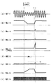
本実施の形態では、上記のような平滑コンデンサ7の電圧増大があった場合でも、下記の動作のように、LED15に過電流が流れることを抑制できる。以下、図2乃至4を用いて、本発明の実施の形態にかかる点灯装置100および照明装置1000の動作を、過電流検出回路54の動作を中心に説明する。図2は、本発明の実施の形態にかかる点灯装置100の動作を示すタイムチャートである。
[Time chart showing operation of lighting device]
In the present embodiment, even when the voltage of the smoothing capacitor 7 increases as described above, it is possible to suppress the overcurrent from flowing through the
図3は、図1の回路図から過電流検出回路54を省略した比較例の回路構成を示す図である。図4は、本発明の実施の形態に対する比較例であり、過電流検出回路54を備えない図3の回路構成における動作を示すタイムチャートである。
FIG. 3 is a diagram showing a circuit configuration of a comparative example in which the
(比較例の動作)
前述したように、過電流検出回路54は、LED15に定格電流を超える過電流が流れたことを検出する回路である。図3は、過電流検出回路54の構成部品である抵抗28、ダイオード29が無い比較例の回路構成を示している。図4はこの比較例の回路の動作をタイミングチャートで示したものであり、以下、図4を用いてその動作および効果を説明する。
(Operation of comparative example)
As described above, the
図4の(a)〜(i)は、図1の回路図中に示す各位置の電圧V1〜V9の電圧波形を示すタイムチャートである。図4(a)に示す電圧V1は商用交流電源1の電圧である。図4(b)に示す電圧V2は平滑コンデンサ7の電圧である。図4(c)に示す電圧V3はコネクタ14aに発生する出力端子の電圧である。図4(d)に示す電圧V4はV3の電圧を分圧した電圧(≒過電圧検出電圧)である。
4A to 4I are time charts showing voltage waveforms of voltages V1 to V9 at respective positions shown in the circuit diagram of FIG. The voltage V1 shown in FIG. 4A is the voltage of the commercial AC power supply 1. The voltage V2 shown in FIG. 4B is the voltage of the smoothing capacitor 7. A voltage V3 shown in FIG. 4C is a voltage at the output terminal generated in the
図4(e)に示す電圧V5は電流検出抵抗13の電圧である。図4(g)に示す電圧V7は制御IC22の保護端子22bの電圧である。図4(h)に示す電圧V8はフィードバック制御回路52のオペアンプ19の出力電圧である。図4(i)に示す電圧V9は制御IC22からの出力電圧(第2スイッチング素子8の動作電圧)である。
The voltage V5 shown in FIG. 4 (e) is the voltage of the
図4においては、抵抗28、ダイオード29を備えない比較例の構成なので、図1に示す電圧V6は存在しない。また、図は模式図であり、動作時のオンデューティ比までは示していない。 In FIG. 4, the voltage V6 shown in FIG. The figure is a schematic diagram and does not show the on-duty ratio during operation.
図4には、3つのタイミングA,B,Cを破線で表している。タイミングAで、図4(a)に示すように商用交流電源1の電圧V1が一時的に低下する。商用交流電源の一時的な電圧低下は、電力会社の送電線の切替えや落雷などが原因で発生する。LED15に過電流が流れる場合として商用交流電源が一時的に電圧低下し復帰した場合などがあげられるので、ここでは動作説明のために商用交流電源の電圧低下時の回路動作を説明するものである。
In FIG. 4, three timings A, B, and C are indicated by broken lines. At timing A, the voltage V1 of the commercial AC power supply 1 temporarily decreases as shown in FIG. The temporary voltage drop of the commercial AC power supply occurs due to the switching of power transmission lines or lightning strikes of the power company. As a case where overcurrent flows through the
商用交流電源1が低下すると、図4(b)に示す平滑コンデンサ7の電圧V2も徐々に低下する。そうすると、フィードバック制御回路52がLED15に流れる電流を一定に制御するので、図4(h)に示すように電圧V8が上昇する。これにより、第2スイッチング素子8のオンデューティ比が大きくなるように制御され、LED15に流れる電流が一定に制御される。
When the commercial AC power supply 1 is lowered, the voltage V2 of the smoothing capacitor 7 shown in FIG. 4B is also gradually lowered. Then, since the feedback control circuit 52 controls the current flowing through the
次に、タイミングBで商用交流電源1が復帰すると、元の正常な電圧となる。ここで、タイミングBからタイミングCの期間にかけて、過渡的な動作が起こる。 Next, when the commercial AC power supply 1 is restored at the timing B, the original normal voltage is obtained. Here, a transitional operation occurs from the timing B to the timing C.
まず、図4(a)に示すように、商用交流電源が電圧低下から正常な電圧に復帰する。これに伴い、図4(b)に示すように、平滑コンデンサ7の電圧も急峻に上昇する。降圧チョッパ回路51の電源となる平滑コンデンサ7が急峻に上昇したことにより、LED15に流れる電流も増加し、図4(e)に示すように電圧V5が急上昇する。
First, as shown in FIG. 4A, the commercial AC power supply returns to a normal voltage from the voltage drop. Along with this, as shown in FIG. 4B, the voltage of the smoothing capacitor 7 also rises steeply. As the smoothing capacitor 7 serving as the power source of the step-down
このとき図4(h)に示すように、電源電圧の低い状態でもLED15に流れる電流を一定にするために、電圧V8すなわちフィードバック制御回路52のオペアンプ出力電圧は高くなっている。つまり、第2スイッチング素子8のデューティ比が大きくなっている状態である。
At this time, as shown in FIG. 4H, the voltage V8, that is, the operational amplifier output voltage of the feedback control circuit 52 is high in order to keep the current flowing through the
前述したように、一般にフィードバック制御は積分回路で行っているため遅れがあり、電源電圧の急峻な変化に追従することは難しい。このため、フィードバック制御回路52の遅れにより電源電圧が急峻な変動に追従できず、オンデューティが適正な制御となっていない状態が生じている。この時、電源電圧に対してオンデューティ比が大きすぎるので、LED15の電流が大きくなりすぎてしまう。
As described above, since feedback control is generally performed by an integrating circuit, there is a delay, and it is difficult to follow a steep change in power supply voltage. For this reason, due to the delay of the feedback control circuit 52, the power supply voltage cannot follow the steep fluctuation, and the on-duty is not controlled properly. At this time, since the on-duty ratio is too large with respect to the power supply voltage, the current of the
LED15は、ほぼ定電圧特性を示すという特徴を持っている。このため、図4(c)に示すように、電圧V3のコネクタ14aの出力端子電圧は、LED15の電流が多く流れることにより高くなるものの、大きくは変化しない。また、図4(d)に示す電圧V4は電圧V3の電圧を分圧したものになるので、図4(c)に示す波形と同様にそれほど大きくは変化しない。
The
図4(g)には、図4(d)の電圧からダイオード26の電圧降下した電圧V7が出力される。上記のとおり電圧V4がそれほど大きな電圧増加とはならないので、電圧V4がさらに電圧降下した電圧V7も大きな電圧増加とはならず、制御端子22bへの入力電圧は保護動作電圧Vpには達しない。その結果、比較例の回路構成では、保護動作は行われない。
In FIG. 4G, a voltage V7 obtained by dropping the voltage of the
保護動作が行われないので、図4(e)に示すように、電圧V5(つまりLED15の電流)が著しく大きな値に到達してしまう。以上のように、図3に示す比較例の回路構成では、商用交流電源1が電圧低下から復帰したときに、LED15に過電流が流れてしまう。
Since the protection operation is not performed, as shown in FIG. 4E, the voltage V5 (that is, the current of the LED 15) reaches a remarkably large value. As described above, in the circuit configuration of the comparative example shown in FIG. 3, when the commercial AC power supply 1 returns from the voltage drop, an overcurrent flows through the
(実施の形態の点灯装置の動作)
次に、図2のタイミングチャートを用いて、上記の比較例の動作と対比して、図1の実施の形態にかかる点灯装置100の動作説明を行う。すなわち、以下、過電流検出回路54を備える場合についての動作説明を行う。
(Operation of lighting device of embodiment)
Next, the operation of the
実施の形態にかかる点灯装置100には過電流検出回路54すなわち抵抗28、ダイオード29が追加されている。これに応じて、図4(f)に、電圧V6が追加されている。電圧V6は、電圧V5が分圧された電圧(「過電流検出電圧」とも称す)である。
An
タイミングAについては図4を用いて述べた比較例の場合と同様であり、ここでは説明を省略する。 Timing A is the same as that in the comparative example described with reference to FIG. 4, and the description thereof is omitted here.
ここで、実施の形態にかかる点灯装置100は過電流検出回路54を備えている点で、比較例とは異なっている。このため、タイミングBからタイミングCの期間の過渡的な動作において、比較例の場合とは異なる動作が実現される。
Here, the
すなわち、LED15に過電流が流れはじめることで、これに応じた電圧が電流検出抵抗13に発生する。過電流検出回路54は、電流検出抵抗13に発生する電圧を分圧して、制御IC22の保護端子22bに出力する。これにより、過電流に応じた電流検出抵抗13での大きな電圧増加に比例して、図2(g)に示す電圧V7も増大することになる。その結果、本実施の形態では、比較例の場合とは異なり、電圧V7が保護端子22bの保護動作電圧Vpに達することになる。従って、LED15に過電流が流れはじめたとき、速やかに制御IC22に所定の保護動作を行わせることができる。
That is, when an overcurrent begins to flow through the
この所定の保護動作とは、本実施の形態では、具体的には、駆動回路9の発振を停止することである。図2(i)を見ると、電圧V9がタイミングBとタイミングCとの間で部分的にローに固定されていることがわかる。 In the present embodiment, the predetermined protection operation is specifically to stop the oscillation of the drive circuit 9. From FIG. 2 (i), it can be seen that the voltage V9 is partially fixed low between timing B and timing C.
この保護動作により第2スイッチング素子8の動作が停止すると、LED電流が供給されなくなる。この間に図2(h)に示すオペアンプ19の出力(電圧V8)が低下する。次に発振を開始するときには、オペアンプ19の出力が低下しており、電源電圧に応じたオンデューティ比で動作しLED15に適正な電流を流すことができる。
When the operation of the
過電圧検出回路53では、コネクタ抜き差しなどによりコネクタ14aに発生する過電圧は検出することはできるが、LED15がほぼ定電圧特性を示すため、LED15の過電流を検出することができない。この点、本実施の形態では、制御IC22の保護端子22bに過電圧検出回路53と過電流検出回路54の両方の出力を接続することで、コネクタ14aの過電圧の検出のみならず、LED15の過電流をも確実に検出できるようにしている。
The
本実施の形態によれば、過電圧検出回路53と過電流検出回路54とで制御IC22の保護端子22bを共用している。そして、保護端子22bへの入力電圧を保護動作電圧Vpと比較するという、共通の比較処理によって、過電圧と過電流の両方を検出している。また、分圧回路の一部を担う抵抗27(分圧抵抗)も、過電圧検出回路53と過電流検出回路54とで共用されている。
According to the present embodiment, the
これらの共用によれば、制御回路およびその制御処理、保護端子、あるいは抵抗といった各構成を、過電圧検出と過電流検出とで別々に設けなくとも済む。制御IC22が過電圧検出回路53と過電流検出回路54の入力に対して共通の制御処理を行うことで、過電圧の検出、過電流の検出、および保護動作の実行を行うことができる。よって、少ない部品点数かつ簡単な構成で、出力電圧の過電圧とLED15の過電流の両方を検出し、保護動作を行うことができる。
By sharing these, it is not necessary to separately provide the control circuit and its control processing, protection terminals, or resistors for overvoltage detection and overcurrent detection. The control IC 22 performs common control processing on the inputs of the
1 商用交流電源、2 整流回路、4 第1スイッチング素子、5 PFC制御IC、7 平滑コンデンサ、8 第2スイッチング素子、9 駆動回路、11 還流ダイオード、13 電流検出抵抗、14a、14b コネクタ、19 オペアンプ、22 制御IC、22a フィードバック制御端子、22b 保護端子、50 昇圧チョッパ回路、51 降圧チョッパ回路、52 フィードバック制御回路、53 過電圧検出回路、54 過電流検出回路、100 点灯装置、1000 照明装置 DESCRIPTION OF SYMBOLS 1 Commercial AC power supply, 2 Rectifier circuit, 4 1st switching element, 5 PFC control IC, 7 Smoothing capacitor, 8 2nd switching element, 9 Drive circuit, 11 Freewheeling diode, 13 Current detection resistor, 14a, 14b Connector, 19 Operational amplifier 22 control IC, 22a feedback control terminal, 22b protection terminal, 50 step-up chopper circuit, 51 step-down chopper circuit, 52 feedback control circuit, 53 overvoltage detection circuit, 54 overcurrent detection circuit, 100 lighting device, 1000 lighting device
Claims (5)
前記出力端子の電圧を検出する電圧検出回路と、
前記発光素子の電流を検出する電流検出回路と、
前記電圧検出回路により検出される検出値と前記電流検出回路により検出される検出値の少なくとも一方が所定値に達したら、前記発光素子へ供給する電流を減少させる制御回路と、
を備え、
前記制御回路は、前記電圧検出回路の検出値と前記電流検出回路の検出値の両方が入力される保護端子を備え、前記保護端子の入力値を前記所定値と比較し、
前記発光素子と直列に接続された電流検出抵抗を備え、
前記電圧検出回路は、
一端が前記出力端子に接続する分圧回路と、
アノードに前記分圧回路で分圧された電圧を受けカソードが前記保護端子と接続する第1ダイオードと、
一端が前記第1ダイオードの前記カソードと前記保護端子との間に接続し他端が前記分圧回路の他端と共通の電位に接続した第一分圧抵抗と、
を含み、
前記電流検出回路は、
一端が前記電流検出抵抗と前記発光素子との間に接続された第二分圧抵抗と、
アノードが前記第二分圧抵抗の他端に接続しカソードが前記第一分圧抵抗の前記一端および前記保護端子に接続した第2ダイオードと、
を含むことを特徴とする点灯装置。 A converter circuit for generating a direct current to be supplied to the output terminal from a direct current voltage rectified by the rectifier circuit, comprising a power supply terminal connected to a rectifier circuit for rectifying an alternating current power supply and an output terminal connected to the light emitting element;
A voltage detection circuit for detecting a voltage of the output terminal;
A current detection circuit for detecting a current of the light emitting element;
A control circuit that reduces a current supplied to the light emitting element when at least one of a detection value detected by the voltage detection circuit and a detection value detected by the current detection circuit reaches a predetermined value;
Equipped with a,
The control circuit includes a protection terminal to which both the detection value of the voltage detection circuit and the detection value of the current detection circuit are input, and compares the input value of the protection terminal with the predetermined value;
A current detection resistor connected in series with the light emitting element;
The voltage detection circuit includes:
A voltage dividing circuit having one end connected to the output terminal;
A first diode that receives a voltage divided by the voltage dividing circuit at an anode and has a cathode connected to the protection terminal;
A first voltage dividing resistor having one end connected between the cathode of the first diode and the protection terminal and the other end connected to a common potential with the other end of the voltage dividing circuit;
Including
The current detection circuit includes:
A second voltage dividing resistor having one end connected between the current detection resistor and the light emitting element;
A second diode having an anode connected to the other end of the second voltage dividing resistor and a cathode connected to the one end of the first voltage dividing resistor and the protection terminal;
The lighting device characterized by including .
整流回路と並列に接続する平滑コンデンサと、
スイッチング素子およびインダクタを備え、前記スイッチング素子が前記平滑コンデンサの一端と前記インダクタの一端との間をスイッチングし、前記インダクタの他端が前記出力端子に接続した降圧チョッパ回路と、
を備え、
前記発光素子と直列に接続された電流検出抵抗を備え、
前記制御回路が、前記電流検出抵抗の電圧を所定電圧に一致させるように前記スイッチング素子のオン時間をフィードバック制御するものであることを特徴とする請求項1または2に記載の点灯装置。 The converter circuit is
A smoothing capacitor connected in parallel with the rectifier circuit;
A step-down chopper circuit comprising a switching element and an inductor, wherein the switching element switches between one end of the smoothing capacitor and one end of the inductor, and the other end of the inductor is connected to the output terminal;
With
A current detection resistor connected in series with the light emitting element;
3. The lighting device according to claim 1, wherein the control circuit performs feedback control of an on-time of the switching element so that a voltage of the current detection resistor matches a predetermined voltage.
前記電圧検出回路及び前記電流検出回路は、前記フィードバック回路の応答速度よりも速い応答速度で、前記検出値を検出することを特徴とする請求項1〜3のいずれか1項に記載の点灯装置。 The converter circuit includes a feedback circuit that feeds back so that a direct current output by the converter circuit has a substantially constant predetermined current value,
The lighting device according to any one of claims 1 to 3, wherein the voltage detection circuit and the current detection circuit detect the detection value at a response speed faster than a response speed of the feedback circuit. .
前記発光素子に電流を供給する、請求項1〜4のいずれか1項に記載の点灯装置と、
を備えることを特徴とする照明装置。 A light emitting element;
The lighting device according to claim 1, wherein a current is supplied to the light emitting element .
A lighting device comprising:
Priority Applications (1)
| Application Number | Priority Date | Filing Date | Title |
|---|---|---|---|
| JP2013103375A JP6182972B2 (en) | 2013-05-15 | 2013-05-15 | Lighting device and lighting device |
Applications Claiming Priority (1)
| Application Number | Priority Date | Filing Date | Title |
|---|---|---|---|
| JP2013103375A JP6182972B2 (en) | 2013-05-15 | 2013-05-15 | Lighting device and lighting device |
Publications (3)
| Publication Number | Publication Date |
|---|---|
| JP2014225360A JP2014225360A (en) | 2014-12-04 |
| JP2014225360A5 JP2014225360A5 (en) | 2016-06-16 |
| JP6182972B2 true JP6182972B2 (en) | 2017-08-23 |
Family
ID=52123899
Family Applications (1)
| Application Number | Title | Priority Date | Filing Date |
|---|---|---|---|
| JP2013103375A Active JP6182972B2 (en) | 2013-05-15 | 2013-05-15 | Lighting device and lighting device |
Country Status (1)
| Country | Link |
|---|---|
| JP (1) | JP6182972B2 (en) |
Families Citing this family (2)
| Publication number | Priority date | Publication date | Assignee | Title |
|---|---|---|---|---|
| WO2016129307A1 (en) * | 2015-02-13 | 2016-08-18 | アイリスオーヤマ株式会社 | Led lighting device |
| DE102018111729A1 (en) | 2017-05-19 | 2018-11-22 | Panasonic Intellectual Property Management Co., Ltd. | Lighting device, luminaire and scoreboard |
Family Cites Families (6)
| Publication number | Priority date | Publication date | Assignee | Title |
|---|---|---|---|---|
| JP2002369507A (en) * | 2001-06-11 | 2002-12-20 | Toko Inc | Switching power unit |
| JP3910941B2 (en) * | 2003-07-02 | 2007-04-25 | 東光株式会社 | Switching constant current power supply |
| JP5006856B2 (en) * | 2008-10-07 | 2012-08-22 | 三菱電機株式会社 | Light emitting device and lighting device |
| JP5320105B2 (en) * | 2009-02-23 | 2013-10-23 | パナソニック株式会社 | LED lighting device and LED lighting apparatus using the same |
| JP2012060743A (en) * | 2010-09-07 | 2012-03-22 | Rohm Co Ltd | Control circuit of dc/dc converter, dc/dc converter using the same, light emitting device and electronic device |
| JP5848046B2 (en) * | 2011-07-06 | 2016-01-27 | 株式会社アイ・ライティング・システム | LED power supply |
-
2013
- 2013-05-15 JP JP2013103375A patent/JP6182972B2/en active Active
Also Published As
| Publication number | Publication date |
|---|---|
| JP2014225360A (en) | 2014-12-04 |
Similar Documents
| Publication | Publication Date | Title |
|---|---|---|
| US9743470B2 (en) | Lighting control circuit, illuminating lamp using the lighting control circuit, and lighting device using the illuminating lamp | |
| US9215769B2 (en) | LED backlight driver system and associated method of operation | |
| US8598802B2 (en) | Triac dimmer compatible WLED driving circuit and method thereof | |
| US9271347B2 (en) | TRIAC dimmable LED driver circuit | |
| US8664880B2 (en) | Ballast/line detection circuit for fluorescent replacement lamps | |
| EP2911474B1 (en) | High voltage converter without auxiliary winding | |
| US20130127356A1 (en) | Led driving power supply apparatus and led lighting apparatus | |
| US8575853B2 (en) | System and method for supplying constant power to luminuous loads | |
| JP2014216310A (en) | Dimming control circuit by fluctuation power source | |
| JP6396336B2 (en) | Power supply circuit that converts the blinking frequency of light emitting diodes | |
| US8937435B1 (en) | Diode bridge | |
| JP6086318B2 (en) | Power supply circuit and lighting device | |
| JP2008166192A (en) | Power supply circuit for driving led | |
| JP2016501436A (en) | LED driver circuit using flyback converter to reduce observable optical flicker by reducing rectified AC power supply ripple | |
| KR20110136537A (en) | Led driving circuit and method for protecting from high voltage and driving with constant current | |
| JP6182972B2 (en) | Lighting device and lighting device | |
| JP2012003996A (en) | Lighting fixture for disaster prevention | |
| KR101267957B1 (en) | Apparatus for control of led lamp | |
| US9055623B1 (en) | Light-emitting diode offline buck converter and method of controlling thereof | |
| KR101553219B1 (en) | Apparatus of driving led | |
| US9125264B2 (en) | Lighting device | |
| KR20180101699A (en) | Led lighting apparatus with interchangeability of fluorescent lamp | |
| JP2019207833A (en) | Power supply device for illumination | |
| JP2014112528A (en) | Light-emitting element lighting device, lighting fixture, and illumination system | |
| JP7429144B2 (en) | LED lighting devices and lighting equipment |
Legal Events
| Date | Code | Title | Description |
|---|---|---|---|
| A521 | Request for written amendment filed |
Free format text: JAPANESE INTERMEDIATE CODE: A523 Effective date: 20160426 |
|
| A621 | Written request for application examination |
Free format text: JAPANESE INTERMEDIATE CODE: A621 Effective date: 20160426 |
|
| A131 | Notification of reasons for refusal |
Free format text: JAPANESE INTERMEDIATE CODE: A131 Effective date: 20170221 |
|
| A977 | Report on retrieval |
Free format text: JAPANESE INTERMEDIATE CODE: A971007 Effective date: 20170223 |
|
| A521 | Request for written amendment filed |
Free format text: JAPANESE INTERMEDIATE CODE: A523 Effective date: 20170323 |
|
| TRDD | Decision of grant or rejection written | ||
| A01 | Written decision to grant a patent or to grant a registration (utility model) |
Free format text: JAPANESE INTERMEDIATE CODE: A01 Effective date: 20170627 |
|
| A61 | First payment of annual fees (during grant procedure) |
Free format text: JAPANESE INTERMEDIATE CODE: A61 Effective date: 20170710 |
|
| R150 | Certificate of patent or registration of utility model |
Ref document number: 6182972 Country of ref document: JP Free format text: JAPANESE INTERMEDIATE CODE: R150 |
|
| R250 | Receipt of annual fees |
Free format text: JAPANESE INTERMEDIATE CODE: R250 |
|
| R250 | Receipt of annual fees |
Free format text: JAPANESE INTERMEDIATE CODE: R250 |
|
| R250 | Receipt of annual fees |
Free format text: JAPANESE INTERMEDIATE CODE: R250 |
|
| R250 | Receipt of annual fees |
Free format text: JAPANESE INTERMEDIATE CODE: R250 |