JP6178516B2 - Refresh scheme for memory cells using next bit table - Google Patents
Refresh scheme for memory cells using next bit table Download PDFInfo
- Publication number
- JP6178516B2 JP6178516B2 JP2016536942A JP2016536942A JP6178516B2 JP 6178516 B2 JP6178516 B2 JP 6178516B2 JP 2016536942 A JP2016536942 A JP 2016536942A JP 2016536942 A JP2016536942 A JP 2016536942A JP 6178516 B2 JP6178516 B2 JP 6178516B2
- Authority
- JP
- Japan
- Prior art keywords
- address
- refresh
- weak
- refreshing
- equal
- Prior art date
- Legal status (The legal status is an assumption and is not a legal conclusion. Google has not performed a legal analysis and makes no representation as to the accuracy of the status listed.)
- Expired - Fee Related
Links
Images


Classifications
-
- G—PHYSICS
- G11—INFORMATION STORAGE
- G11C—STATIC STORES
- G11C11/00—Digital stores characterised by the use of particular electric or magnetic storage elements; Storage elements therefor
- G11C11/21—Digital stores characterised by the use of particular electric or magnetic storage elements; Storage elements therefor using electric elements
- G11C11/34—Digital stores characterised by the use of particular electric or magnetic storage elements; Storage elements therefor using electric elements using semiconductor devices
- G11C11/40—Digital stores characterised by the use of particular electric or magnetic storage elements; Storage elements therefor using electric elements using semiconductor devices using transistors
- G11C11/401—Digital stores characterised by the use of particular electric or magnetic storage elements; Storage elements therefor using electric elements using semiconductor devices using transistors forming cells needing refreshing or charge regeneration, i.e. dynamic cells
- G11C11/406—Management or control of the refreshing or charge-regeneration cycles
-
- G—PHYSICS
- G06—COMPUTING; CALCULATING OR COUNTING
- G06F—ELECTRIC DIGITAL DATA PROCESSING
- G06F12/00—Accessing, addressing or allocating within memory systems or architectures
- G06F12/02—Addressing or allocation; Relocation
- G06F12/0207—Addressing or allocation; Relocation with multidimensional access, e.g. row/column, matrix
-
- G—PHYSICS
- G11—INFORMATION STORAGE
- G11C—STATIC STORES
- G11C11/00—Digital stores characterised by the use of particular electric or magnetic storage elements; Storage elements therefor
- G11C11/21—Digital stores characterised by the use of particular electric or magnetic storage elements; Storage elements therefor using electric elements
- G11C11/34—Digital stores characterised by the use of particular electric or magnetic storage elements; Storage elements therefor using electric elements using semiconductor devices
- G11C11/40—Digital stores characterised by the use of particular electric or magnetic storage elements; Storage elements therefor using electric elements using semiconductor devices using transistors
- G11C11/401—Digital stores characterised by the use of particular electric or magnetic storage elements; Storage elements therefor using electric elements using semiconductor devices using transistors forming cells needing refreshing or charge regeneration, i.e. dynamic cells
- G11C11/406—Management or control of the refreshing or charge-regeneration cycles
- G11C11/40615—Internal triggering or timing of refresh, e.g. hidden refresh, self refresh, pseudo-SRAMs
-
- G—PHYSICS
- G11—INFORMATION STORAGE
- G11C—STATIC STORES
- G11C11/00—Digital stores characterised by the use of particular electric or magnetic storage elements; Storage elements therefor
- G11C11/21—Digital stores characterised by the use of particular electric or magnetic storage elements; Storage elements therefor using electric elements
- G11C11/34—Digital stores characterised by the use of particular electric or magnetic storage elements; Storage elements therefor using electric elements using semiconductor devices
- G11C11/40—Digital stores characterised by the use of particular electric or magnetic storage elements; Storage elements therefor using electric elements using semiconductor devices using transistors
- G11C11/401—Digital stores characterised by the use of particular electric or magnetic storage elements; Storage elements therefor using electric elements using semiconductor devices using transistors forming cells needing refreshing or charge regeneration, i.e. dynamic cells
- G11C11/406—Management or control of the refreshing or charge-regeneration cycles
- G11C11/40618—Refresh operations over multiple banks or interleaving
-
- G—PHYSICS
- G11—INFORMATION STORAGE
- G11C—STATIC STORES
- G11C11/00—Digital stores characterised by the use of particular electric or magnetic storage elements; Storage elements therefor
- G11C11/21—Digital stores characterised by the use of particular electric or magnetic storage elements; Storage elements therefor using electric elements
- G11C11/34—Digital stores characterised by the use of particular electric or magnetic storage elements; Storage elements therefor using electric elements using semiconductor devices
- G11C11/40—Digital stores characterised by the use of particular electric or magnetic storage elements; Storage elements therefor using electric elements using semiconductor devices using transistors
- G11C11/401—Digital stores characterised by the use of particular electric or magnetic storage elements; Storage elements therefor using electric elements using semiconductor devices using transistors forming cells needing refreshing or charge regeneration, i.e. dynamic cells
- G11C11/406—Management or control of the refreshing or charge-regeneration cycles
- G11C11/40622—Partial refresh of memory arrays
-
- G—PHYSICS
- G11—INFORMATION STORAGE
- G11C—STATIC STORES
- G11C2211/00—Indexing scheme relating to digital stores characterized by the use of particular electric or magnetic storage elements; Storage elements therefor
- G11C2211/401—Indexing scheme relating to cells needing refreshing or charge regeneration, i.e. dynamic cells
- G11C2211/406—Refreshing of dynamic cells
- G11C2211/4061—Calibration or ate or cycle tuning
-
- G—PHYSICS
- G11—INFORMATION STORAGE
- G11C—STATIC STORES
- G11C2211/00—Indexing scheme relating to digital stores characterized by the use of particular electric or magnetic storage elements; Storage elements therefor
- G11C2211/401—Indexing scheme relating to cells needing refreshing or charge regeneration, i.e. dynamic cells
- G11C2211/406—Refreshing of dynamic cells
- G11C2211/4065—Low level details of refresh operations
Landscapes
- Engineering & Computer Science (AREA)
- Microelectronics & Electronic Packaging (AREA)
- Computer Hardware Design (AREA)
- Physics & Mathematics (AREA)
- Theoretical Computer Science (AREA)
- Mathematical Physics (AREA)
- General Engineering & Computer Science (AREA)
- General Physics & Mathematics (AREA)
- Dram (AREA)
Description
関連出願の相互参照
本出願は、参照によりその全体が本明細書に組み込まれる、2013年12月9日に出願された「REFRESH SCHEME FOR MEMORY CELLS WITH NEXT BIT TABLE」という名称の米国仮特許出願第61/913,788号の利益を主張する。
This application is a U.S. provisional patent application entitled `` REFRESH SCHEME FOR MEMORY CELLS WITH NEXT BIT TABLE '' filed Dec. 9, 2013, which is incorporated herein by reference in its entirety. Claim the benefit of 61 / 913,788.
本開示は、電子メモリ動作に関し、より詳細には、弱保持時間(Weak Retention Time)をもつメモリセルのためのリフレッシュ方式に関する。 The present disclosure relates to electronic memory operation, and more particularly, to a refresh scheme for memory cells having weak retention times.
半導体メモリデバイスは、たとえば、スタティックランダムアクセスメモリ(SRAM)およびダイナミックランダムアクセスメモリ(DRAM)を含む。DRAMメモリセルは概して、1つのトランジスタおよび1つのキャパシタを含み、それによって、高度の統合をもたらす。キャパシタは、対応するビット値(たとえば、0または1)として情報を記憶するために充電されるか、または放電され得る。キャパシタは電荷を漏電するので、記憶された情報は、キャパシタ電荷が周期的にリフレッシュされない限り、最終的に減衰する。リフレッシュ要件により、DRAMは、SRAMおよび他のスタティックメモリとは対照的にダイナミックメモリと呼ばれる。DRAMの連続的なリフレッシュは、概して、その使用をコンピュータメインメモリに限定する。 Semiconductor memory devices include, for example, static random access memory (SRAM) and dynamic random access memory (DRAM). DRAM memory cells generally include one transistor and one capacitor, thereby providing a high degree of integration. A capacitor can be charged or discharged to store information as a corresponding bit value (eg, 0 or 1). Since the capacitor leaks charge, the stored information will eventually decay unless the capacitor charge is periodically refreshed. Due to refresh requirements, DRAM is called dynamic memory as opposed to SRAM and other static memory. The continuous refresh of DRAM generally limits its use to computer main memory.
DRAMスケーリングは、DRAMチップごとのビット総数を増加させ続け、セルの値を可読に保つプロセスであるDRAMリフレッシュの仕様に直接影響を及ぼす。DRAMリフレッシュの仕様は、リフレッシュコマンドが各DRAMに送られる間隔(tREFI)と、リフレッシュコマンドがDRAMインターフェースを占有する時間量(tRFC)とを含む。残念ながら、DRAMスケーリングは、弱保持セル(たとえば、減少した保持時間を有するセル)の数を増加させる。そのようなセルは、記憶された情報を維持するために追加のリフレッシュサイクルを伴う。チップまたは他の同様のコンピュータアーキテクチャ上のシステムにおけるリフレッシュサイクルの増加により、性能および電力消費量への顕著な影響がもたらされる。場合によっては、リフレッシュサイクルの増加なしに潜在的なDRAMチップ歩留まり損失が生じる。 DRAM scaling directly affects the specification of DRAM refresh, a process that keeps increasing the total number of bits per DRAM chip and keeping the cell values readable. The DRAM refresh specification includes an interval (tREFI) at which a refresh command is sent to each DRAM and an amount of time (tRFC) that the refresh command occupies the DRAM interface. Unfortunately, DRAM scaling increases the number of weak retention cells (eg, cells with reduced retention time). Such cells involve additional refresh cycles to maintain stored information. Increasing refresh cycles in a system on a chip or other similar computer architecture has a significant impact on performance and power consumption. In some cases, potential DRAM chip yield loss occurs without an increase in refresh cycles.
メモリコントローラ内のメモリリフレッシュ方法は、リフレッシュアドレスカウンタからリフレッシュアドレスを読むステップと、弱アドレス表から弱アドレスを読むステップとを含み得る。本方法はまた、弱アドレスに組み合わせられたネクストビットシーケンスに少なくとも部分的に基づいて次の弱アドレスを生成するステップと、リフレッシュアドレスを弱アドレスおよび次の弱アドレスと比較するステップとを含む。本方法は、リフレッシュサイクルをスキップすることと、リフレッシュアドレスをリフレッシュすることと、弱アドレスをリフレッシュすることと、リフレッシュアドレスと弱アドレスの両方をリフレッシュすることとの間で選択するステップをさらに含む。前記選択するステップは、リフレッシュアドレスと弱アドレスおよび次の弱アドレスとの比較に少なくとも部分的に基づいている。 A memory refresh method in the memory controller may include reading a refresh address from a refresh address counter and reading a weak address from a weak address table. The method also includes generating a next weak address based at least in part on the next bit sequence combined with the weak address, and comparing the refresh address with the weak address and the next weak address. The method further includes selecting between skipping a refresh cycle, refreshing the refresh address, refreshing the weak address, and refreshing both the refresh address and the weak address. The selecting step is based at least in part on a comparison of the refresh address with the weak address and the next weak address.
メモリリフレッシュ装置は、リフレッシュアドレスを記憶するように動作可能なリフレッシュカウンタと、弱アドレスを記憶するように動作可能な弱アドレス表とを含み得る。本装置は、弱アドレスに組み合わせられたネクストビット表内のネクストビット値に少なくとも部分的に基づいて次の弱アドレスを生成するように動作可能なネクストビット表をさらに含む。本装置はまた、リフレッシュサイクルをスキップすることと、リフレッシュアドレスをリフレッシュすることと、弱アドレスをリフレッシュすることと、リフレッシュアドレスと弱アドレスの両方をリフレッシュすることとの間で選択するように動作可能なリフレッシュコントローラを含む。リフレッシュコントローラは、リフレッシュアドレスを弱アドレスおよび次の弱アドレスと比較することに少なくとも部分的に基づいて、この選択を行う。 The memory refresh apparatus may include a refresh counter operable to store refresh addresses and a weak address table operable to store weak addresses. The apparatus further includes a next bit table operable to generate a next weak address based at least in part on the next bit value in the next bit table combined with the weak address. The device is also operable to select between skipping the refresh cycle, refreshing the refresh address, refreshing the weak address, and refreshing both the refresh address and the weak address. Including a refresh controller. The refresh controller makes this selection based at least in part on comparing the refresh address with the weak address and the next weak address.
メモリコントローラ装置は、リフレッシュアドレスを記憶するためのリフレッシュカウンタと、弱アドレスを記憶するための弱アドレス表とを含み得る。本装置は、弱アドレスに組み合わせられたネクストビット表内のネクストビット値に少なくとも部分的に基づいて次の弱アドレスを生成するためのネクストビット表をさらに含む。本装置はまた、リフレッシュアドレスを弱アドレスおよび次の弱アドレスと比較することに少なくとも部分的に基づいて、リフレッシュサイクルをスキップすることと、リフレッシュアドレスをリフレッシュすることと、弱アドレスをリフレッシュすることと、リフレッシュアドレスと弱アドレスの両方をリフレッシュすることとの間で選択するための手段を含む。 The memory controller device may include a refresh counter for storing refresh addresses and a weak address table for storing weak addresses. The apparatus further includes a next bit table for generating a next weak address based at least in part on the next bit value in the next bit table combined with the weak address. The apparatus also skips a refresh cycle, refreshes the refresh address, and refreshes the weak address based at least in part on comparing the refresh address with the weak address and the next weak address. Means for selecting between refreshing both the refresh address and the weak address.
本開示の別の態様は、非一時的コンピュータ可読媒体がプログラムコードを記録された、メモリリフレッシュのためのコンピュータプログラム製品を含む。プログラムコードは、リフレッシュカウンタ内にリフレッシュアドレスを記憶するためのプログラムコードと、弱アドレス表内に弱アドレスを記憶するためのプログラムコードと、弱アドレスに組み合わせられたネクストビット表内のネクストビット値に少なくとも部分的に基づいて次の弱アドレスを生成するためのプログラムコードとを含む。プログラムコードはまた、リフレッシュアドレスを弱アドレスおよび次の弱アドレスと比較することに少なくとも部分的に基づいて、リフレッシュサイクルをスキップすることと、リフレッシュアドレスをリフレッシュすることと、弱アドレスをリフレッシュすることと、リフレッシュアドレスと弱アドレスの両方をリフレッシュすることとの間で選択するためのプログラムコードを含む。 Another aspect of the present disclosure includes a computer program product for memory refresh, in which a non-transitory computer readable medium has recorded program code. The program code includes the program code for storing the refresh address in the refresh counter, the program code for storing the weak address in the weak address table, and the next bit value in the next bit table combined with the weak address. Program code for generating a next weak address based at least in part. The program code also skips the refresh cycle, refreshes the refresh address, and refreshes the weak address based at least in part on comparing the refresh address with the weak address and the next weak address. Includes program code for selecting between refreshing both the refresh address and the weak address.
上記は、続く詳細な説明をよりよく理解することができるように、本開示の特徴および技術的利点について、かなり大まかに概説したものである。本開示のさらなる特徴および利点について、以下で説明する。本開示は、本開示と同じ目的を果たすための他の構造を修正または設計するための基礎として容易に利用できることを、当業者には理解されたい。そのような均等な構成が、添付の特許請求の範囲に記載の本開示の教示から逸脱しないことも、当業者は理解されたい。本開示の構成と動作方法の両方に関して本開示の特徴になると考えられる新規の特徴が、さらなる目的および利点とともに、以下の説明を添付の図と併せて検討することからよりよく理解されるであろう。しかしながら、図の各々は、例示および説明を目的として提供されているに過ぎず、本開示の制限を定めるものではないことを、明確に理解されたい。 The foregoing has outlined rather broadly the features and technical advantages of the present disclosure in order that the detailed description that follows may be better understood. Additional features and advantages of the present disclosure are described below. Those skilled in the art will appreciate that the present disclosure can be readily utilized as a basis for modifying or designing other structures to serve the same purpose as the present disclosure. It should also be appreciated by those skilled in the art that such equivalent constructions do not depart from the teachings of the present disclosure as set forth in the appended claims. The novel features believed to be features of this disclosure in terms of both the configuration and method of operation of this disclosure, together with further objects and advantages, will be better understood from a consideration of the following description in conjunction with the accompanying figures. Let's go. However, it should be clearly understood that each of the figures is provided for purposes of illustration and description only and does not define limitations of the present disclosure.
本開示のより完全な理解のために、ここで、添付の図面と併せて以下の説明を参照する。 For a more complete understanding of the present disclosure, reference is now made to the following description, taken in conjunction with the accompanying drawings, in which:
添付の図面に関して以下に記載される詳細な説明は、様々な構成の説明として意図されており、本明細書で説明される概念が実施され得る唯一の構成を表すことを意図されていない。詳細な説明は、様々な概念の完全な理解を与えるための具体的な詳細を含む。しかしながら、これらの概念がこれらの具体的な詳細がなくても実施することができることは当業者に明らかであろう。いくつかの例では、そのような概念を不明瞭にすることを避けるために、よく知られている構造および構成要素がブロック図形式で示される。本明細書の説明では、「および/または」という用語の使用は、「包含的論理和」を表すことが意図され、「または」という用語の使用は、「排他的論理和」を表すことが意図される。 The detailed description set forth below in connection with the appended drawings is intended as a description of various configurations and is not intended to represent the only configurations in which the concepts described herein may be implemented. The detailed description includes specific details for providing a thorough understanding of various concepts. However, it will be apparent to those skilled in the art that these concepts can be practiced without these specific details. In some instances, well-known structures and components are shown in block diagram form in order to avoid obscuring such concepts. In the description herein, the use of the term “and / or” is intended to represent “inclusive OR” and the use of the term “or” represents “exclusive OR”. Intended.
ダイナミックランダムアクセスメモリ(DRAM)スケーリングは、DRAMチップ当たりのビット総数を増加させ続けている。容量のこの増加は、ビットセルの値が可読に保たれるプロセスであるDRAMリフレッシュの仕様に直接影響を及ぼす。DRAMリフレッシュの仕様は、リフレッシュコマンドが各DRAMに送られる間隔(tREFI)と、リフレッシュコマンドがDRAMインターフェースを占有する時間量(tRFC)とを含む。残念ながら、DRAMスケーリングは、弱保持セル(たとえば、減少した保持時間を有するセル)の数をも増加させる。そのようなセルは、記憶された情報を維持するために増加したリフレッシュサイクルを伴う。性能および電力消費量は、チップ(SoC)または他の同様のコンピュータアーキテクチャ上のシステムにおけるDRAM上のリフレッシュサイクルの増加により著しく影響を及ぼされる。弱保持セルの数の増加からの潜在的なDRAMチップ歩留まり損失がリフレッシュサイクルの増加なしに生じる。 Dynamic random access memory (DRAM) scaling continues to increase the total number of bits per DRAM chip. This increase in capacity directly affects the DRAM refresh specification, the process by which bit cell values are kept readable. The DRAM refresh specification includes an interval (tREFI) at which a refresh command is sent to each DRAM and an amount of time (tRFC) that the refresh command occupies the DRAM interface. Unfortunately, DRAM scaling also increases the number of weak retention cells (eg, cells with reduced retention time). Such cells involve increased refresh cycles to maintain the stored information. Performance and power consumption are significantly affected by the increase in refresh cycles on DRAM in systems on a chip (SoC) or other similar computer architecture. Potential DRAM chip yield loss from an increase in the number of weak retention cells occurs without an increase in refresh cycles.
本開示の一態様は、リフレッシュ期間(たとえば、リフレッシュ間隔tREFI)の名目上の増加に伴って、弱保持状態をもつセルに対するリフレッシュサイクルを挿入する。一構成では、リフレッシュコントローラは、弱セルに対するリフレッシュ動作を挿入すること、および/または強セルに対するリフレッシュサイクルをスキップすることの間で選択し得る。この構成では、リフレッシュコントローラは、リフレッシュアドレスを弱アドレスおよび次の弱アドレスと比較することに少なくとも部分的に基づいて、リフレッシュサイクルをスキップすることと、リフレッシュアドレスをリフレッシュすることと、弱アドレスをリフレッシュすることと、リフレッシュアドレスと弱アドレスの両方をリフレッシュすることとの間で選択する。 One aspect of the present disclosure inserts a refresh cycle for cells having a weak retention state with a nominal increase in the refresh period (eg, refresh interval tREFI). In one configuration, the refresh controller may select between inserting a refresh operation for a weak cell and / or skipping a refresh cycle for a strong cell. In this configuration, the refresh controller skips the refresh cycle, refreshes the refresh address, and refreshes the weak address based at least in part on comparing the refresh address with the weak address and the next weak address. And to refresh both the refresh address and the weak address.
図1Aおよび図1Bは、他のメモリセルのためのリフレッシュ頻度を維持しながら、弱保持状態をもつメモリセル(たとえば、行)のリフレッシュ頻度を増加させるための既存の技法を示す回路タイミング図を示す。図1Aは、リフレッシュアドレス120に対してリフレッシュ動作を実行するためのダブルリフレッシュサイクル110をもつタイミング図100を示す。ダブルリフレッシュサイクル110は、たとえば、32ミリ秒(ms)のリフレッシュ仕様の場合には16ミリ秒(ms)であり得る。この例では、弱保持状態を有するリフレッシュアドレス122をもつ4行のメモリがある。典型的には、リフレッシュアドレス0、1、2、および3に対してリフレッシュ動作が実行される。ただし、この例では、後続のパス中でリフレッシュアドレス124と、リフレッシュアドレス126と、リフレッシュアドレス128とに対するリフレッシュ動作がスキップされる。図1Aに示すように、通常の保持状態をもつリフレッシュアドレスに対するリフレッシュサイクルをスキップしながら、弱保持状態を有するリフレッシュアドレス122に対するリフレッシュサイクルが倍化される。
1A and 1B are circuit timing diagrams illustrating existing techniques for increasing the refresh frequency of memory cells (e.g., rows) with weak retention states while maintaining the refresh frequency for other memory cells. Show. FIG. 1A shows a timing diagram 100 with a
図1Bは、リフレッシュアドレス170に対してリフレッシュ動作を実行するためにシングルリフレッシュサイクル160を用いる所望のタイミング図150を示す。シングルリフレッシュサイクル160は、たとえば、32ミリ秒(ms)であり得る。この例では、同じく、弱保持状態を有するリフレッシュアドレス172をもつ4行のメモリがある。典型的には、弱保持状態をもつリフレッシュアドレス172に対して挿入リフレッシュ動作180が実行される。この例では、弱行リフレッシュサイクルが挿入される。図1Bに示すように、通常の保持状態をもつリフレッシュアドレスに対するリフレッシュサイクルを維持しながら、弱保持状態をもつリフレッシュアドレス172のみに対するリフレッシュサイクルが倍化される。リフレッシュの増加により、リフレッシュ間隔(tREFI)がわずかに増加するが、弱セルの数は、通常のセルの数に対して極めて少ない。その間隔の増加がより小さいために、図1Bに示すリフレッシュサイクルは、図1Aに示すリフレッシュサイクルと比較して好都合であり得る。
FIG. 1B shows a desired timing diagram 150 that uses a
いくつかの環境では、外部の(1×)リフレッシュ速度に基づいて弱メモリセルに対するダブル(2×)リフレッシュ速度を提供することに限定される既存のリフレッシュ方式は、メモリリソースを浪費する。たとえば、いくつかの弱メモリセルをリフレッシュするために1.5×リフレッシュ速度またはいくつかの他のリソースが、2×リフレッシュ速度よりも好適であり得る環境では、リソースが節約され得る。 In some environments, existing refresh schemes that are limited to providing double (2 ×) refresh rates for weak memory cells based on external (1 ×) refresh rates waste memory resources. For example, in an environment where 1.5 × refresh rate or some other resource may be preferred over 2 × refresh rate to refresh some weak memory cells, resources may be saved.
本開示の一態様は、外部の1×リフレッシュ速度に基づいてフレキシブルな内部のリフレッシュ速度を可能にするメモリリフレッシュ制御技法を含む。本開示の別の態様は、外部の1×リフレッシュ速度に基づいて強メモリ行に対するリフレッシュサイクルをスキップすることを可能にするメモリリフレッシュ制御技法を含む。 One aspect of the present disclosure includes a memory refresh control technique that allows a flexible internal refresh rate based on an external 1 × refresh rate. Another aspect of the present disclosure includes a memory refresh control technique that allows skipping refresh cycles for strong memory rows based on an external 1 × refresh rate.
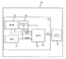
図2Aは、本開示の一態様による、メモリブロック260に結合されたリフレッシュ制御ブロック210を含むメモリコントローラ200を示すブロック図である。この構成では、リフレッシュ制御ブロック210は、リフレッシュカウンタ220、弱行表(weak row table)230、NEXT BIT表240、およびリフレッシュ制御論理250を含む。図2Bにさらに示す弱行表230は、対応する弱保持状態をもつメモリアドレス(たとえば、弱アドレス(WADD))のみを含む。
FIG. 2A is a block diagram illustrating a
NEXT BIT表240は、弱行表230に対応する。NEXT BIT表240は、対応する弱行に対して1.5×リフレッシュ速度または2×リフレッシュ速度を実装するための、本開示の態様によるデータ構造体である。リフレッシュ制御論理250は、リフレッシュする次の行がどれであるべきかを決定する。NEXT BIT表240は、行リフレッシュをリフレッシュシーケンス内のどこに挿入すべきかを決定することによって適切なリフレッシュ速度を実装する。
The NEXT BIT table 240 corresponds to the weak row table 230. The NEXT BIT table 240 is a data structure according to aspects of the present disclosure for implementing a 1.5 × refresh rate or 2 × refresh rate for the corresponding weak row.
図3Aは、弱行表230(図2B)内の項目に対応する事前プログラムされる保持ビット302を含む表300である。事前プログラムされる保持ビット302は、弱行表230(図2B)に記載された各それぞれの行に適用されるリフレッシュ速度304を規定する。事前プログラムされる保持ビット302は、行が通常の行であるか、または弱行であるか、および弱行が2×リフレッシュ速度または1.5×リフレッシュ速度を受けるべきかどうかに基づいて事前プログラムされ得る。保持ビット表では、本開示のこの態様によれば、保持ビット値00は外部の1×リフレッシュ速度における通常のリフレッシュを示し、保持ビット値01はメモリセルの弱行に適用される1.5×リフレッシュ速度を示し、保持ビット値10はメモリセルの弱行に適用される2×リフレッシュ速度を示す。この例では、保持ビット値11は、利用不可能なリフレッシュ速度、またはメモリセルの対応する行に適用される代替のリフレッシュ速度を示す。
FIG. 3A is a table 300 that includes
NEXT BIT306は、保持ビットに基づいて規定される。NEXT BIT306は、次の弱アドレス(NEXT_WADD)を生成するために弱アドレスと組み合わされる。図3Bに示すように、本開示の態様によれば、2×リフレッシュ速度を実装するためにNEXT BIT306に単一ビットのサイクル310が使用される場合があり、1.5×リフレッシュ速度を実装するために2ビットのNEXT BITサイクル312が使用される場合がある。図3Cは、本開示の一態様による、次の弱アドレス316を生成するためのNEXT BIT306と弱アドレス314との組合せを示す。図3Cに示す例は、次の弱アドレス316を生成するためにNEXT BIT306のうちの2つが使用される、1.5×リフレッシュ速度の実装形態である。2×リフレッシュ速度を実装するためには、次の弱アドレス316を生成するのに、NEXT BIT306のうちの1つのみが使用され、NEXT BIT306のうちの第2番目は無視される。
本開示の一態様によれば、2×リフレッシュサイクルでは、次の弱アドレス316を生成するために、NEXT BIT306のうちの現在の単一のビットが、弱アドレス314のコピー内の最上位ビットと入れ替わる。1.5×リフレッシュサイクルでは、次の弱アドレス316を生成するために、NEXT BIT306のうちの2つの現在のビットが、弱アドレス314のコピー内の2つの最上位ビットと入れ替わる。
According to one aspect of the present disclosure, in a 2 × refresh cycle, the current single bit of
図4は、本開示の一態様による、弱保持状態をもつメモリセルのためのリフレッシュ方式を示すフローチャート400である。ブロック410では、どのNEXT BITを使用すべきかを決定するために、保持ビット(RET)が読まれる。ブロック412〜416において、リフレッシュアドレス(REFADD)、弱行アドレス(WADD)、および次の弱行アドレス(NEXT_WADD)が比較される。
FIG. 4 is a
リフレッシュアドレスが弱行アドレスに等しくなく、リフレッシュアドレスが次の弱行アドレスに等しくない場合、ブロック418において、リフレッシュアドレスがリフレッシュされる(たとえば、第1の基準)。本開示の態様によれば、リフレッシュアドレスが弱行アドレスに等しくないが、リフレッシュアドレスが次の弱行アドレスに等しい場合、ブロック420において、リフレッシュアドレスと弱行アドレスの両方がリフレッシュされる(たとえば、第2の基準)。
If the refresh address is not equal to the weak row address and the refresh address is not equal to the next weak row address, at
リフレッシュアドレスが弱行アドレスに等しいが、リフレッシュアドレスが次の弱行アドレスに等しくない場合、ブロック422において、リフレッシュアドレスがスキップされる(たとえば、第3の基準)。リフレッシュアドレスが弱行アドレスに等しく、リフレッシュアドレスが次の弱行アドレスに等しい場合、ブロック424において、弱行アドレスがリフレッシュされる(たとえば、第4の基準)。ブロック426および428では、すべての弱行アドレスがリフレッシュされた後、NEXT BIT(N0,N1)の値が保持ビットに基づいて更新され、次の弱行アドレスがNEXT BIT(N0,N1)に基づいて変更される。次いで、リフレッシュサイクルが開始402から繰り返される。
If the refresh address is equal to the weak row address, but the refresh address is not equal to the next weak row address, at
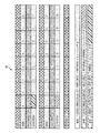
図5は、本開示の一態様による、2×速度リフレッシュサイクルの一例を示す表500を示す。表500は、2×速度リフレッシュ動作の各サイクルに対する、REFADD、WADD、およびNEXT_WADDの値を含む。図5に示す例では、アドレス行0は、弱アドレスである。例示的なリフレッシュシーケンスは、リフレッシュ行アドレス0からリフレッシュ行アドレス15までの、16行メモリおよびサイクルをリフレッシュすることに基づいている。たとえば、実用的な実装形態は、16K行または32K行を有するはるかに大きいメモリを含み得る(たとえば、8Kを超える行をもつDRAMに関して、複数の行がグループ化され同時にリフレッシュされ、通常、8K「行グループ」が存在し、各リフレッシュコマンドが1つのグループをリフレッシュする)ことを理解されたい。REFADDの値は、0から15まで循環し、次いで0に戻る。この例では、1つの弱行(行0)しか存在しないので、WADDの値は常に0である。NEXT_WADD値は、0に初期化され、次いで、弱アドレスがリフレッシュされるたびに変化する。
FIG. 5 shows a table 500 illustrating an example of a 2 × speed refresh cycle in accordance with an aspect of the present disclosure. Table 500 includes values for REFADD, WADD, and NEXT_WADD for each cycle of a 2 × speed refresh operation. In the example shown in FIG. 5,
図5に示す例では、第1のリフレッシュサイクル(REFADD=0)が上述の第4の基準を満たすので、第1のリフレッシュサイクル中にWADDのみがリフレッシュされる。その後、NEXT BITが更新され、それに応じて、NEXT_WADDも、NEXT BITによって示される量だけ更新される。この例では、NEXT_WADDは、2×リフレッシュ例におけるNEXT BIT値1に対応する8に更新される。REFADD=1からREFADD=7までの次の7つのリフレッシュサイクルの各々が条件1を満たすので、通常の1×リフレッシュのみが行われる。
In the example shown in FIG. 5, since the first refresh cycle (REFADD = 0) satisfies the above-mentioned fourth criterion, only WADD is refreshed during the first refresh cycle. Thereafter, NEXT BIT is updated, and NEXT_WADD is also updated accordingly by the amount indicated by NEXT BIT. In this example, NEXT_WADD is updated to 8 corresponding to
第9のリフレッシュサイクル(たとえば、REFADD=8)が上述の第2の基準を満たすので、同じサイクルにおいて、通常のリフレッシュと弱行リフレッシュの両方が行われる(たとえば、REFADD=8とWADD=0の両方がリフレッシュされる)。このサイクルにおいてWADDがリフレッシュされたので、NEXT BIT、およびそれに応じてNEXT_WADDが再び更新される。この例では、NEXT_WADDが0に更新される。次いで、第10〜第16のリフレッシュサイクル(たとえば、REFADD=9からREFADD=15まで)では、16個のメモリアドレスの1つの全リフレッシュ期間を完了するために、通常のリフレッシュのみが行われる。次いで、リフレッシュシーケンスが繰り返される。リフレッシュされた行の得られたシーケンスは、0、1、2、3、4、5、6、7、(8および0)、9、10、11、12、13、14、15であり、シーケンス中に弱行0が2回リフレッシュされたことを示す。
Since the ninth refresh cycle (for example, REFADD = 8) meets the second criterion described above, both normal refresh and weak row refresh are performed in the same cycle (for example, REFADD = 8 and WADD = 0 Both are refreshed). Since WADD was refreshed in this cycle, NEXT BIT and NEXT_WADD are updated again accordingly. In this example, NEXT_WADD is updated to 0. Next, in the 10th to 16th refresh cycles (for example, from REFADD = 9 to REFADD = 15), only normal refresh is performed in order to complete one full refresh period of 16 memory addresses. The refresh sequence is then repeated. The resulting sequence of refreshed rows is 0, 1, 2, 3, 4, 5, 6, 7, (8 and 0), 9, 10, 11, 12, 13, 14, 15, and the sequence Indicates that
図6は、本開示の一態様による、1.5×速度リフレッシュサイクルの一例を示す表600を示す。表600は、1.5×速度リフレッシュ動作の各サイクルに対する、REFADD、WADD、およびNEXT_WADDの値を含む。図6に示す例では、アドレス行0は、弱アドレスである。REFADDの値は、0から15まで循環し、次いで0に戻る。この例では、1つの弱行(行0)しか存在しないので、WADDの値は常に0である。NEXT_WADD値は、0に初期化され、次いで、弱アドレスがリフレッシュされるたびに変化する。
FIG. 6 shows a table 600 illustrating an example of a 1.5 × rate refresh cycle in accordance with an aspect of the present disclosure. Table 600 includes REFADD, WADD, and NEXT_WADD values for each cycle of a 1.5 × speed refresh operation. In the example shown in FIG. 6,
1.5×リフレッシュ速度の実装形態では、本開示の態様によれば、2つのNEXT BITは、図3Bに示すように00、11、10、01からのパターンで変化する。対応するNEXT_WADDは、上述のように0から12、12から8、8から2、および2から0のパターンで再び変化する。この例では、サイクル0において、図4を参照しながら上述した4つの基準に基づいて、弱行リフレッシュのみが実行される。第11のリフレッシュサイクル(REFADD=12)では、4つの基準に基づいて、通常のリフレッシュ(メモリ行アドレス12)と弱行リフレッシュ(メモリ行アドレス0)の両方が再び実行される。第12〜第14のサイクル(REFADD=13〜REFADD=15)は、4つの基準に基づいて通常の動作を受ける。リフレッシュシーケンスの第2ラウンドにおけるREFADD=0である、第17のサイクルでは、第3の基準を満たすので、リフレッシュがスキップされる。リフレッシュシーケンスの第2ラウンドにおけるREFADD=8である、第25のサイクルでは、上述の4つの基準に基づいて、行8と行0の両方がリフレッシュされる。この例は、本開示の態様による、1.5×リフレッシュ速度でリフレッシュされる弱行を示す。
In a 1.5 × refresh rate implementation, according to aspects of the present disclosure, the two NEXT BITs change in a pattern from 00, 11, 10, 01 as shown in FIG. 3B. The corresponding NEXT_WADD changes again in the
本開示の別の態様によれば、弱行表は、強保持を有するメモリアドレスに関していくつかのリフレッシュサイクルのスキップを容易にするための強行アドレスも含み得る。これにより、強メモリセルに関して、外部の1×リフレッシュ速度よりも低いリフレッシュ速度を実装することが可能になる。図7Aを参照すると、保持ビット表700内の保持ビット値11は、メモリセルの強行に関して外部の1×リフレッシュ速度よりも低いリフレッシュ速度を示し得る。
According to another aspect of the present disclosure, the weak row table may also include a strong row address to facilitate skipping some refresh cycles for memory addresses that have strong hold. This makes it possible to implement a refresh rate lower than the external 1 × refresh rate for strong memory cells. Referring to FIG. 7A, the retained
図7Aは、弱行表230(図2B)内の項目に対応する事前プログラムされる保持ビット702を含む表700を示す。事前プログラムされる保持ビット702は、弱行表230(図2B)に記載された各それぞれの行に適用されるリフレッシュ速度704を規定する。事前プログラムされる保持ビット702は、たとえば、行が通常の行であるか、または弱行であるか、および弱行が2×リフレッシュ速度保護または1.5×リフレッシュ速度を受けるべきかどうかに基づいて事前プログラムされる。本開示の態様による保持ビット表のこの例では、保持ビット値00は外部の1×リフレッシュ速度における通常のリフレッシュを示し、保持ビット値01はメモリセルの弱行に適用される1.5×リフレッシュ速度を示し、保持ビット値10はメモリセルの弱行に適用される2×リフレッシュ速度を示す。たとえば、保持ビット値11は、0.5×リフレッシュ速度が強メモリセルの対応する行に適用されていることを示し得る。
FIG. 7A shows a table 700 that includes
NEXT BIT706は、0.5×リフレッシュ速度を実装するために11に設定されている事前プログラムされる保持ビット702に基づいて規定される。図7Bに示すように、保持ビットが11に設定されるとき、利用されるNEXT BITは単一ビット(たとえば、N1)であり、他方のNEXT BIT(たとえば、N0)は無視される。0.5×リフレッシュ速度を実装するために事前プログラムされる保持ビット702が11に設定されるとき、サイクル中に強行がリフレッシュされるかどうかにかかわらず、強行アドレスのすべてのリフレッシュサイクルの後、NEXT BITは、その状態を変化させる。
図7Cは、本開示の一態様による、強行リフレッシュの動作をさらに示す。事前プログラムされる保持ビット702が11に設定される際、NEXT BIT(N1)706が1に設定されるときだけ、対応する強行アドレス710がリフレッシュされる。各リフレッシュサイクルの後、NEXT BIT(N1)706が0に設定される。これは、1つおきにリフレッシュサイクルをスキップさせ、それによって、強行アドレス710に対して0.5×リフレッシュ速度を実装する。したがって、本開示の一態様によれば、強アドレスの1つのリフレッシュサイクル内の通常のリフレッシュ動作と、強アドレスの次のリフレッシュサイクルをスキップすることとの間で交互に行うために、NEXT BIT706が使用される。
FIG. 7C further illustrates a forced refresh operation according to an aspect of the present disclosure. When the preprogrammed
本開示の一態様によるメモリコントローラ装置は、リフレッシュアドレスを記憶するためのリフレッシュカウンタと、弱アドレスを記憶するための弱アドレス表と、弱アドレスに組み合わせられたネクストビット表内のネクストビット値に少なくとも部分的に基づいて次の弱アドレスを生成するためのネクストビット表とを含む。メモリコントローラは、リフレッシュアドレスを弱アドレスおよび次の弱アドレスと比較することに少なくとも部分的に基づいて、リフレッシュサイクルをスキップすることと、リフレッシュアドレスをリフレッシュすることと、弱アドレスをリフレッシュすることと、リフレッシュアドレスと弱アドレスの両方をリフレッシュすることとの間で選択するための手段を含み得る。本開示のこの態様によれば、選択するための前記手段は、図2Aに示すリフレッシュ制御論理250を含み得る。
A memory controller device according to an aspect of the present disclosure includes at least a refresh counter for storing a refresh address, a weak address table for storing a weak address, and a next bit value in a next bit table combined with the weak address. And a next bit table for generating the next weak address based in part. The memory controller is based at least in part on comparing the refresh address with the weak address and the next weak address, skipping the refresh cycle, refreshing the refresh address, refreshing the weak address; Means may be included to select between refreshing both the refresh address and the weak address. According to this aspect of the present disclosure, the means for selecting may include the
メモリコントローラ装置はまた、リフレッシュアドレスに対応する少なくとも1つの保持ビットを読むための手段と、保持ビットに基づいてリフレッシュ速度を決定するための手段と、保持ビットに基づいてネクストビットシーケンスを決定するための手段と、弱アドレスの各リフレッシュの後、ネクストビットシーケンスに従ってネクストビットを変更するための手段とを含み得る。保持ビットを読み、リフレッシュ速度を決定し、ネクストビットシーケンスを決定し、ネクストビットを変更するための手段は、図2Aに示すように構成された、リフレッシュカウンタ220、弱行表230、NEXT BIT表240、およびリフレッシュ制御論理を含み得る。
The memory controller device also includes means for reading at least one retained bit corresponding to the refresh address, means for determining a refresh rate based on the retained bit, and determining a next bit sequence based on the retained bit And means for changing the next bit according to the next bit sequence after each refresh of the weak address. The means for reading the retained bits, determining the refresh rate, determining the next bit sequence, and changing the next bit are the
本開示の一態様によれば、メモリコントローラ装置はまた、リフレッシュアドレスが弱アドレスに等しく、次の弱アドレスに等しくないとき、リフレッシュサイクルをスキップするための手段と、リフレッシュアドレスが弱アドレスに等しくなく、次の弱アドレスに等しくないとき、リフレッシュアドレスをリフレッシュするための手段と、リフレッシュアドレスが弱アドレスに等しく、次の弱アドレスに等しいとき、弱アドレスをリフレッシュするための手段と、リフレッシュアドレスが弱アドレスに等しくなく、次の弱アドレスに等しいとき、リフレッシュアドレスと弱アドレスの両方をリフレッシュするための手段とを含み得る。リフレッシュサイクルをスキップするための手段、リフレッシュアドレスをリフレッシュするための手段、弱アドレスをリフレッシュするための手段、およびリフレッシュアドレスと弱アドレスの両方をリフレッシュするための手段は、図2Aに示すように構成された、リフレッシュカウンタ220、弱行表230、NEXT BIT表240、およびリフレッシュ制御論理を含み得る。
According to one aspect of the present disclosure, the memory controller device also includes means for skipping a refresh cycle when the refresh address is equal to the weak address and not equal to the next weak address, and the refresh address is not equal to the weak address. Means for refreshing the refresh address when not equal to the next weak address; means for refreshing the weak address when the refresh address is equal to the weak address and equal to the next weak address; and the refresh address is weak And means for refreshing both the refresh address and the weak address when not equal to the address and equal to the next weak address. Means for skipping the refresh cycle, means for refreshing the refresh address, means for refreshing the weak address, and means for refreshing both the refresh address and the weak address are configured as shown in FIG.
メモリ制御システムの態様を、様々な装置および方法を参照して提示する。これらの装置および方法は、以下の発明を実施するための形態において説明され、様々なブロック、モジュール、構成要素、回路、ステップ、プロセス、アルゴリズムなど(「要素」と総称される)によって添付の図面に示される。これらの要素は、電子ハードウェア、コンピュータソフトウェア、またはそれらの任意の組合せを使用して実装され得る。そのような要素をハードウェアとして実装するか、またはソフトウェアとして実装するかは、具体的な適用例およびシステム全体に課された設計制約に依存する。 Aspects of a memory control system are presented with reference to various devices and methods. These apparatus and methods are described in the following Detailed Description, and are included in the accompanying drawings by various blocks, modules, components, circuits, steps, processes, algorithms, etc. (collectively referred to as “elements”). Shown in These elements may be implemented using electronic hardware, computer software, or any combination thereof. Whether such elements are implemented as hardware or software depends on the specific application and design constraints imposed on the overall system.
例として、要素、もしくは要素の任意の部分、または要素の任意の組合せは、1つまたは複数のプロセッサを含む「処理システム」で実装され得る。プロセッサの例としては、マイクロプロセッサ、マイクロコントローラ、デジタル信号プロセッサ(DSP)、フィールドプログラマブルゲートアレイ(FPGA)、プログラマブル論理デバイス(PLD)、ステートマシン、ゲート論理、個別ハードウェア回路、および本開示全体にわたって説明される様々な機能を実行するように構成された他の適切なハードウェアがある。処理システム内の1つまたは複数のプロセッサは、ソフトウェアを実行することができる。ソフトウェアは、ソフトウェア、ファームウェア、ミドルウェア、マイクロコード、ハードウェア記述言語、または他の名称で呼ばれるかどうかを問わず、命令、命令セット、コード、コードセグメント、プログラムコード、プログラム、サブプログラム、ソフトウェアモジュール、アプリケーション、ソフトウェアアプリケーション、ソフトウェアパッケージ、ルーチン、サブルーチン、オブジェクト、実行可能ファイル、実行スレッド、手順、機能などを意味するように広く解釈されるべきである。 By way of example, an element, or any portion of an element, or any combination of elements may be implemented with a “processing system” that includes one or more processors. Examples of processors include microprocessors, microcontrollers, digital signal processors (DSPs), field programmable gate arrays (FPGAs), programmable logic devices (PLDs), state machines, gate logic, discrete hardware circuits, and throughout this disclosure There are other suitable hardware configured to perform the various functions described. One or more processors in the processing system may execute software. Software, whether called software, firmware, middleware, microcode, hardware description language, or other names, instructions, instruction sets, code, code segments, program code, programs, subprograms, software modules, It should be interpreted broadly to mean applications, software applications, software packages, routines, subroutines, objects, executables, threads of execution, procedures, functions, etc.
したがって、1つまたは複数の例示的な構成では、説明される機能は、ハードウェア、ソフトウェア、ファームウェア、またはそれらの任意の組合せに実装することができる。ソフトウェアで実装される場合、機能は、1つもしくは複数の命令またはコードとして非一時的コンピュータ可読媒体上に記憶されるか、あるいは非一時的コンピュータ可読媒体上で符号化され得る。コンピュータ可読媒体は、コンピュータ記憶媒体を含む。記憶媒体は、コンピュータによってアクセスされ得る任意の利用可能な媒体であり得る。限定ではなく例として、そのようなコンピュータ可読媒体は、RAM、ROM、EEPROM、CD-ROMもしくは他の光ディスクストレージ、磁気ディスクストレージもしくは他の磁気記憶デバイス、または、命令もしくはデータ構造の形態の所望のプログラムコードを搬送もしくは記憶するために使用することができ、コンピュータによってアクセスすることができる、任意の他の媒体を含み得る。上記の組合せもコンピュータ可読媒体の範囲の中に含まれるべきである。 Thus, in one or more exemplary configurations, the functions described can be implemented in hardware, software, firmware, or any combination thereof. If implemented in software, the functions may be stored on the non-transitory computer readable medium as one or more instructions or code, or encoded on the non-transitory computer readable medium. Computer-readable media includes computer storage media. A storage media may be any available media that can be accessed by a computer. By way of example, and not limitation, such computer readable media can be RAM, ROM, EEPROM, CD-ROM or other optical disk storage, magnetic disk storage or other magnetic storage device, or any desired form in the form of instructions or data structures. Any other medium that can be used to carry or store the program code and that can be accessed by a computer can be included. Combinations of the above should also be included within the scope of computer-readable media.
図8は、本開示の一態様を有利に用いることができる例示的なワイヤレス通信システム800を示す。説明のために、図8は、3つの遠隔ユニット820、830、および850と、2つの基地局840とを示す。一般的なワイヤレス通信システムは、これよりも多くの遠隔ユニットおよび基地局を有し得ることが認識されよう。遠隔ユニット820、830、および850は、以下でさらに説明する本開示の態様であるメモリコントローラ回路825A、825B、および825Cをそれぞれ含む。図8は、基地局840から遠隔ユニット820、830、および850への順方向リンク信号880と、リモートユニット820、830、および850から基地局840への逆方向リンク信号890とを示す。
FIG. 8 illustrates an example
図8では、ワイヤレスローカルループシステムにおいて、遠隔ユニット820は携帯電話として示され、遠隔ユニット830はポータブルコンピュータとして示され、遠隔ユニット850は定位置遠隔ユニットとして示されている。たとえば、遠隔ユニットは、セルフォン、ハンドヘルドパーソナル通信システム(PCS)ユニット、携帯情報端末などのポータブルデータユニット、またはメータ読取り機器などの固定位置データユニットとすることができる。図8は、本開示の教示によるメモリコントローラ回路を示すが、本開示は、これらの例示的な図示のユニットに限定されない。たとえば、本開示の態様によるメモリコントローラ回路は、任意のデバイスにおいて最適に用いられ得る。
In FIG. 8, in the wireless local loop system,
特定の回路が説明されたが、当業者は、本開示を実施するために、開示された回路のすべてが必要とされるわけではないことを理解されよう。その上、本開示に対する注目を維持するために、いくつかのよく知られている回路は記載されなかった。同様に、説明はいくつかのロケーションにおける論理「0」および論理「1」に言及しているが、本開示の動作に影響を及ぼすことなく、論理値は入れ替えることができ、それに応じて回路の残りの部分が調整されることを当業者は諒解する。 Although specific circuits have been described, those skilled in the art will appreciate that not all of the disclosed circuits are required to implement the present disclosure. Moreover, some well-known circuits have not been described in order to maintain attention to the present disclosure. Similarly, the description refers to logic “0” and logic “1” at several locations, but the logic values can be interchanged without affecting the operation of the present disclosure, and the circuit's accordingly. Those skilled in the art will appreciate that the remainder is adjusted.
様々な装置および方法に関連して、いくつかのプロセッサが説明されてきた。これらのプロセッサは、電子ハードウェア、コンピュータソフトウェア、またはそれらの任意の組合せを使用して実装され得る。そのようなプロセッサがハードウェアとして実装されるか、ソフトウェアとして実装されるかは、具体的な用途およびシステムに課される全体的な設計制約に依存する。例として、プロセッサ、プロセッサの任意の部分、または、本開示で提示されるプロセッサの任意の組合せは、マイクロプロセッサ、マイクロコントローラ、デジタル信号プロセッサ(DSP)、フィールドプログラマブルゲートアレイ(FPGA)、プログラマブル論理デバイス(PLD)、ステートマシン、ゲート論理、個別ハードウェア回路、および、本開示全体にわたって説明された様々な機能を実行するように構成された他の適切な処理構成要素で実装され得る。本開示で提示されるプロセッサ、プロセッサの任意の部分、またはプロセッサの任意の組合せの機能は、マイクロプロセッサ、マイクロコントローラ、DSP、または他の適切なプラットフォームによって実行されているソフトウェアにより実装され得る。 A number of processors have been described in connection with various apparatus and methods. These processors may be implemented using electronic hardware, computer software, or any combination thereof. Whether such a processor is implemented as hardware or software depends on the specific application and the overall design constraints imposed on the system. By way of example, a processor, any portion of a processor, or any combination of processors presented in this disclosure may be a microprocessor, microcontroller, digital signal processor (DSP), field programmable gate array (FPGA), programmable logic device (PLD), state machine, gate logic, discrete hardware circuitry, and other suitable processing components configured to perform the various functions described throughout this disclosure. The functionality of the processor, any portion of the processor, or any combination of processors presented in this disclosure may be implemented by software running on a microprocessor, microcontroller, DSP, or other suitable platform.
ソフトウェアは、ソフトウェア、ファームウェア、ミドルウェア、マイクロコード、ハードウェア記述言語、または他の名称で呼ばれるかどうかを問わず、命令、命令セット、コード、コードセグメント、プログラムコード、プログラム、サブプログラム、ソフトウェアモジュール、アプリケーション、ソフトウェアアプリケーション、ソフトウェアパッケージ、ルーチン、サブルーチン、オブジェクト、実行可能ファイル、実行スレッド、手順、機能などを意味するように広く解釈されるべきである。ソフトウェアは、非一時的コンピュータ可読媒体上に存在する場合がある。コンピュータ可読媒体は、例として、磁気記憶デバイス(たとえば、ハードディスク、フロッピーディスク、磁気ストリップ)、光ディスク(たとえば、コンパクトディスク(CD)、デジタル多用途ディスク(DVD))、スマートカード、フラッシュメモリデバイス(たとえば、カード、スティック、キードライブ)、ランダムアクセスメモリ(RAM)、読取り専用メモリ(ROM)、プログラマブルROM(PROM)、消去可能PROM(EPROM)、電気的消去可能PROM(EEPROM)、レジスタ、またはリムーバブルディスクのようなメモリを含み得る。メモリは、本開示全体にわたって提示した様々な態様ではプロセッサとは別個に示されているが、メモリはプロセッサの内部にあり得る(たとえば、キャッシュまたはレジスタ)。 Software, whether called software, firmware, middleware, microcode, hardware description language, or other names, instructions, instruction sets, code, code segments, program code, programs, subprograms, software modules, It should be interpreted broadly to mean applications, software applications, software packages, routines, subroutines, objects, executables, threads of execution, procedures, functions, etc. The software may reside on a non-transitory computer readable medium. Computer readable media include, by way of example, magnetic storage devices (e.g., hard disks, floppy disks, magnetic strips), optical disks (e.g., compact disks (CDs), digital versatile disks (DVDs)), smart cards, flash memory devices (e.g., , Cards, sticks, key drives), random access memory (RAM), read-only memory (ROM), programmable ROM (PROM), erasable PROM (EPROM), electrically erasable PROM (EEPROM), register, or removable disk Such a memory may be included. Although the memory is shown separately from the processor in various aspects presented throughout this disclosure, the memory may be internal to the processor (eg, a cache or a register).
コンピュータ可読媒体はコンピュータプログラム製品において具体化され得る。例として、コンピュータプログラム製品は、パッケージング材料中のコンピュータ可読媒体を含み得る。当業者は、特定の適用例および全体的なシステムに課された設計制約全体に応じて、本開示全体にわたって提示された記載の機能を最もよく実装する方法を認識されよう。 The computer readable medium may be embodied in a computer program product. By way of example, a computer program product may include a computer readable medium in packaging material. Those skilled in the art will recognize how best to implement the described functionality presented throughout this disclosure, depending on the particular application and the overall design constraints imposed on the overall system.
本明細書で説明した、様々な例示的なブロック、モジュール、要素、構成要素、方法、およびアルゴリズムは、電子ハードウェア、コンピュータソフトウェア、または両方の組合せとして実装され得ることを当業者は諒解されよう。さらに、これらは、説明したこととは別に区分され得る。ハードウェアとソフトウェアのこの互換性を説明するために、様々な例示的なセクション、ブロック、モジュール、要素、構成要素、方法、およびアルゴリズムを、上記では概してそれらの機能に関して説明してきた。そのような機能が、ハードウェアまたはソフトウェアのどちらとして実施されるのかは、具体的な適用例と、システム全体に課せられる設計制約とによって決まる。当業者は、各特定の用途のために様々な方法で説明した機能を実装することができる。 Those skilled in the art will appreciate that the various exemplary blocks, modules, elements, components, methods, and algorithms described herein can be implemented as electronic hardware, computer software, or a combination of both. . Furthermore, these can be separated separately from what has been described. To illustrate this interchangeability of hardware and software, various exemplary sections, blocks, modules, elements, components, methods, and algorithms have been described above generally in terms of their functionality. Whether such functionality is implemented as hardware or software depends on the specific application and the design constraints imposed on the overall system. Those skilled in the art can implement the functions described in various ways for each particular application.
開示されたプロセスにおけるステップまたはブロックの特定の順序または階層は、例示的な手法の説明であることを理解されたい。設計上の選好に基づいて、プロセスにおけるステップまたはブロックの特定の順序または階層が並べ替えられてもよいことを理解されたい。添付の方法クレームは、様々なステップの要素を例示的な順序で提示したものであり、提示された特定の順序または階層に限定されることを意味するものではない。 It should be understood that the specific order or hierarchy of steps or blocks in the disclosed process is a description of exemplary approaches. It should be understood that a particular order or hierarchy of steps or blocks in the process may be rearranged based on design preferences. The accompanying method claims present elements of the various steps in a sample order, and are not meant to be limited to the specific order or hierarchy presented.
本開示およびその利点について詳しく説明したが、添付の特許請求の範囲によって規定される本開示の趣旨および範囲から逸脱することなく、本明細書において様々な変更、代用および改変を行うことができることは理解されたい。さらに、本出願の範囲は、本明細書で説明したプロセス、機械、製造、組成物、手段、方法、およびステップの特定の構成に限定されるものではない。当業者が本開示から容易に諒解するように、本明細書で説明した対応する構成と実質的に同じ機能を実行するか、または実質的に同じ結果を実現する、現存するまたは今後開発されるプロセス、機械、製造、組成物、手段、方法、またはステップが、本開示に従って利用され得る。したがって、添付の特許請求の範囲は、そのようなプロセス、機械、製造、組成物、手段、方法、またはステップをそれらの範囲内に含むものとする。 Although the present disclosure and its advantages have been described in detail, various changes, substitutions and modifications can be made herein without departing from the spirit and scope of the present disclosure as defined by the appended claims. I want you to understand. Further, the scope of the present application is not limited to the particular configuration of processes, machines, manufacture, compositions, means, methods, and steps described herein. As those skilled in the art will readily appreciate from this disclosure, existing or future developed that perform substantially the same function or achieve substantially the same results as the corresponding configurations described herein. Any process, machine, manufacture, composition, means, method, or step may be utilized in accordance with the present disclosure. Accordingly, the appended claims are intended to include within their scope such processes, machines, manufacture, compositions of matter, means, methods, or steps.
本開示の前述の説明は、いかなる当業者も本開示を作製または使用できるようにするために提供される。本開示に対する様々な修正形態が当業者には容易に明らかとなり、本明細書で定義する一般原理は、本開示の趣旨または範囲から逸脱することなく、他の変形形態に適用され得る。したがって、本開示は、本明細書で説明される例および設計に限定されるものではなく、本明細書で開示される原理および新規の特徴に合致する最も広い範囲を与えられるべきである。 The previous description of the disclosure is provided to enable any person skilled in the art to make or use the disclosure. Various modifications to the present disclosure will be readily apparent to those skilled in the art, and the generic principles defined herein may be applied to other variations without departing from the spirit or scope of the disclosure. Accordingly, the present disclosure is not intended to be limited to the examples and designs described herein, but is to be accorded the widest scope consistent with the principles and novel features disclosed herein.
100 タイミング図
110 ダブルリフレッシュサイクル
120 リフレッシュアドレス
122 弱保持状態を有するリフレッシュアドレス
124 リフレッシュアドレス
126 リフレッシュアドレス
128 リフレッシュアドレス
150 タイミング図
160 シングルリフレッシュサイクル
170 リフレッシュアドレス
172 弱保持状態を有するリフレッシュアドレス
180 挿入リフレッシュ動作
200 メモリコントローラ
210 リフレッシュ制御ブロック
220 リフレッシュカウンタ
230 弱行表
240 NEXT BIT表
250 リフレッシュ制御論理
260 メモリブロック
300 表
302 事前プログラムされる保持ビット
304 リフレッシュ速度
306 NEXT BIT
310 単一ビットのサイクル
312 2ビットのNEXT BITサイクル
314 弱アドレス
316 次の弱アドレス
700 保持ビット表
702 事前プログラムされる保持ビット
704 リフレッシュ速度
706 NEXT BIT
710 強行アドレス
800 ワイヤレス通信システム
820 遠隔ユニット、携帯電話
825A メモリコントローラ回路
825B メモリコントローラ回路
825C メモリコントローラ回路
830 遠隔ユニット、ポータブルコンピュータ
840 基地局
850 遠隔ユニット、定位置遠隔ユニット
880 順方向リンク信号
890 逆方向リンク信号
100 Timing diagram
110 Double refresh cycle
120 refresh address
122 Refresh address with weak hold state
124 Refresh address
126 Refresh address
128 refresh address
150 Timing diagram
160 single refresh cycle
170 Refresh address
172 Refresh address with weak hold state
180 Insert refresh operation
200 Memory controller
210 Refresh control block
220 Refresh counter
230 Weak Table
240 NEXT BIT table
250 Refresh control logic
260 memory blocks
300 tables
302 Pre-programmed retention bit
304 refresh rate
306 NEXT BIT
310 single bit cycle
312 2-bit NEXT BIT cycle
314 Weak address
316 Next weak address
700 Retention bit table
702 Preprogrammed retention bit
704 refresh rate
706 NEXT BIT
710 forced address
800 wireless communication system
820 Remote unit, mobile phone
825A memory controller circuit
825B memory controller circuit
825C memory controller circuit
830 Remote unit, portable computer
840 base station
850 remote unit, fixed position remote unit
880 Forward link signal
890 Reverse link signal
Claims (11)
リフレッシュアドレスカウンタからリフレッシュアドレスを読むステップと、
弱アドレス表から弱アドレスを読むステップと、
前記リフレッシュアドレスに対応する保持ビットによって規定されるリフレッシュ速度に従ってビットシーケンスを決定するステップと、
前記弱アドレスの一部分に組み合わせられた前記ビットシーケンスに少なくとも部分的に基づいて次の弱アドレスの値を生成するステップと、
前記リフレッシュアドレスを前記弱アドレスおよび前記次の弱アドレスの値と比較するステップと、
前記比較に少なくとも部分的に基づいて、リフレッシュサイクルをスキップすることと、前記リフレッシュアドレスをリフレッシュすることと、前記弱アドレスをリフレッシュすることと、前記リフレッシュアドレスと前記弱アドレスの両方をリフレッシュすることとの間で選択するステップと
を含む、方法。 A memory refresh method in a memory controller, comprising:
Reading the refresh address from the refresh address counter;
Reading weak addresses from the weak address table;
Determining a bit sequence according to a refresh rate defined by a retained bit corresponding to the refresh address;
Generating a value for a next weak address based at least in part on the bit sequence combined with a portion of the weak address;
Comparing the refresh address with the value of the weak address and the next weak address;
Skipping a refresh cycle, refreshing the refresh address, refreshing the weak address, refreshing both the refresh address and the weak address based at least in part on the comparison And selecting between.
前記リフレッシュアドレスが前記弱アドレスに等しくなく、前記次の弱アドレスに等しくないとき、前記リフレッシュアドレスをリフレッシュするステップと、
前記リフレッシュアドレスが前記弱アドレスに等しく、前記次の弱アドレスに等しいとき、前記弱アドレスをリフレッシュするステップと、
前記リフレッシュアドレスが前記弱アドレスに等しくなく、前記次の弱アドレスに等しいとき、前記リフレッシュアドレスと前記弱アドレスの両方をリフレッシュするステップと
をさらに含む、請求項1に記載の方法。 Skipping the refresh cycle when the refresh address is equal to the weak address and not equal to the next weak address;
Refreshing the refresh address when the refresh address is not equal to the weak address and not equal to the next weak address;
Refreshing the weak address when the refresh address is equal to the weak address and equal to the next weak address;
The method of claim 1, further comprising: refreshing both the refresh address and the weak address when the refresh address is not equal to the weak address and equal to the next weak address.
前記強アドレスのリフレッシュサイクルをスキップするステップと
をさらに含む、請求項1に記載の方法。 Reading a strong address from the weak address table;
2. The method of claim 1, further comprising skipping the strong address refresh cycle.
弱アドレスを記憶するための弱アドレス表と、
前記弱アドレスの一部分に組み合わせられたビット表内のビットシーケンスに少なくとも部分的に基づいて次の弱アドレスの生成を可能にするためのビット表と、
前記リフレッシュアドレスに対応する保持ビットによって規定されるリフレッシュ速度に従って前記ビットシーケンスを決定するための手段と、前記リフレッシュアドレスを前記弱アドレスおよび前記次の弱アドレスと比較することに少なくとも部分的に基づいて、リフレッシュサイクルをスキップすることと、前記リフレッシュアドレスをリフレッシュすることと、前記弱アドレスをリフレッシュすることと、前記リフレッシュアドレスと前記弱アドレスの両方をリフレッシュすることとの間で選択するための手段と
を含む、メモリコントローラ装置。 A refresh counter for storing the refresh address;
A weak address table for storing weak addresses;
A bit table for enabling generation of a next weak address based at least in part on a bit sequence in a bit table combined with a portion of the weak address;
Based at least in part on means for determining the bit sequence according to a refresh rate defined by a retained bit corresponding to the refresh address, and comparing the refresh address with the weak address and the next weak address Means for selecting between skipping a refresh cycle, refreshing the refresh address, refreshing the weak address, and refreshing both the refresh address and the weak address; Including a memory controller device.
をさらに含む、請求項6に記載のメモリコントローラ装置。 7. The memory controller device according to claim 6 , further comprising means for changing a next bit sequence according to the bit sequence after each refresh of the weak address.
前記リフレッシュアドレスが前記弱アドレスに等しくなく、前記次の弱アドレスに等しくないとき、前記リフレッシュアドレスをリフレッシュするための手段と、
前記リフレッシュアドレスが前記弱アドレスに等しく、前記次の弱アドレスに等しいとき、前記弱アドレスをリフレッシュするための手段と、
前記リフレッシュアドレスが前記弱アドレスに等しくなく、前記次の弱アドレスに等しいとき、前記リフレッシュアドレスと前記弱アドレスの両方をリフレッシュするための手段と
をさらに含む、請求項6に記載のメモリコントローラ装置。 Means for skipping the refresh cycle when the refresh address is equal to the weak address and not equal to the next weak address;
Means for refreshing the refresh address when the refresh address is not equal to the weak address and not equal to the next weak address;
Means for refreshing the weak address when the refresh address is equal to the weak address and equal to the next weak address;
7. The memory controller device according to claim 6 , further comprising means for refreshing both the refresh address and the weak address when the refresh address is not equal to the weak address and equal to the next weak address.
リフレッシュカウンタ内にリフレッシュアドレスを記憶するためのプログラムコードと、
弱アドレス表内に弱アドレスを記憶するためのプログラムコードと、
前記リフレッシュアドレスに対応する保持ビットによって規定されるリフレッシュ速度に従ってビットシーケンスを決定するためのプログラムコードと、
前記弱アドレスの一部分に組み合わせられたビット表内の前記ビットシーケンスに少なくとも部分的に基づいて次の弱アドレスを生成するためのプログラムコードと、
前記リフレッシュアドレスを前記弱アドレスおよび前記次の弱アドレスと比較することに少なくとも部分的に基づいて、リフレッシュサイクルをスキップすることと、前記リフレッシュアドレスをリフレッシュすることと、前記弱アドレスをリフレッシュすることと、前記リフレッシュアドレスと前記弱アドレスの両方をリフレッシュすることとの間で選択するためのプログラムコードと
を含む、コンピュータプログラム。 A computer program for memory refresh, including program code, wherein the program code is
Program code for storing the refresh address in the refresh counter;
Program code for storing weak addresses in the weak address table;
A program code for determining a bit sequence according to a refresh rate defined by a holding bit corresponding to the refresh address;
Program code for generating a next weak address based at least in part on the bit sequence in a bit table combined with a portion of the weak address;
Skipping a refresh cycle, refreshing the refresh address, and refreshing the weak address based at least in part on comparing the refresh address with the weak address and the next weak address. And a program code for selecting between refreshing both the refresh address and the weak address.
前記弱アドレスの各リフレッシュの後、前記ビットシーケンスに従ってネクストビットシーケンスを変更するためのプログラムコード
をさらに含む、請求項10に記載のコンピュータプログラム。 The program code is
11. The computer program according to claim 10 , further comprising program code for changing a next bit sequence according to the bit sequence after each refresh of the weak address.
Applications Claiming Priority (5)
| Application Number | Priority Date | Filing Date | Title |
|---|---|---|---|
| US201361913788P | 2013-12-09 | 2013-12-09 | |
| US61/913,788 | 2013-12-09 | ||
| US14/276,452 US9230634B2 (en) | 2013-12-09 | 2014-05-13 | Refresh scheme for memory cells with next bit table |
| US14/276,452 | 2014-05-13 | ||
| PCT/US2014/066726 WO2015088740A1 (en) | 2013-12-09 | 2014-11-20 | Refresh scheme for memory cells with next bit table |
Publications (3)
| Publication Number | Publication Date |
|---|---|
| JP2016540337A JP2016540337A (en) | 2016-12-22 |
| JP2016540337A5 JP2016540337A5 (en) | 2017-07-13 |
| JP6178516B2 true JP6178516B2 (en) | 2017-08-09 |
Family
ID=53271839
Family Applications (1)
| Application Number | Title | Priority Date | Filing Date |
|---|---|---|---|
| JP2016536942A Expired - Fee Related JP6178516B2 (en) | 2013-12-09 | 2014-11-20 | Refresh scheme for memory cells using next bit table |
Country Status (6)
| Country | Link |
|---|---|
| US (1) | US9230634B2 (en) |
| EP (1) | EP3055864B1 (en) |
| JP (1) | JP6178516B2 (en) |
| KR (1) | KR101766875B1 (en) |
| CN (1) | CN105814639A (en) |
| WO (1) | WO2015088740A1 (en) |
Families Citing this family (6)
| Publication number | Priority date | Publication date | Assignee | Title |
|---|---|---|---|---|
| US9640242B1 (en) * | 2015-12-02 | 2017-05-02 | Qualcomm Incorporated | System and method for temperature compensated refresh of dynamic random access memory |
| US10754988B2 (en) * | 2016-08-30 | 2020-08-25 | Winbond Electronics Corporation | Anti-rollback version upgrade in secured memory chip |
| KR20180049314A (en) * | 2016-10-31 | 2018-05-11 | 에스케이하이닉스 주식회사 | Circuit for counting address, memory device and method for operating memory device |
| KR20180136611A (en) | 2017-06-14 | 2018-12-26 | 에스케이하이닉스 주식회사 | Semiconductor device |
| KR20220048857A (en) | 2020-10-13 | 2022-04-20 | 에스케이하이닉스 주식회사 | Memory device and operating method thereof |
| CN118351907A (en) * | 2023-01-09 | 2024-07-16 | 长鑫存储技术有限公司 | Refreshing circuit, method and memory |
Family Cites Families (10)
| Publication number | Priority date | Publication date | Assignee | Title |
|---|---|---|---|---|
| US5644545A (en) * | 1996-02-14 | 1997-07-01 | United Memories, Inc. | Bimodal refresh circuit and method for using same to reduce standby current and enhance yields of dynamic memory products |
| US7020038B2 (en) | 2004-05-05 | 2006-03-28 | Taiwan Semiconductor Manufacturing Co., Ltd. | Efficient refresh operation for semiconductor memory devices |
| KR20110030779A (en) | 2009-09-18 | 2011-03-24 | 삼성전자주식회사 | Memory device and memory system having the same and method of controlling the same |
| KR101879442B1 (en) * | 2011-05-25 | 2018-07-18 | 삼성전자주식회사 | Method of refreshing a volatile memory device, refresh address generator and volatile memory device |
| DE102012203610A1 (en) | 2011-05-25 | 2012-11-29 | Samsung Electronics Co., Ltd. | Method for refreshing memory device e.g. Rambus dynamic RAM, involves selecting third address from pool of addresses with range defined by significant bits of one of first and second address, to perform respective refresh to cell |
| US8971094B2 (en) | 2011-09-16 | 2015-03-03 | Inphi Corporation | Replacement of a faulty memory cell with a spare cell for a memory circuit |
| KR20130078455A (en) | 2011-12-30 | 2013-07-10 | 삼성전자주식회사 | Semiconductor memory device storing memory characteristic information, memory module and memory system having the same and operating method thereof |
| KR101966858B1 (en) | 2012-04-24 | 2019-04-08 | 삼성전자주식회사 | Method of operating a volatile memory device, volatile memory device and method of controlling memory system |
| KR101975029B1 (en) | 2012-05-17 | 2019-08-23 | 삼성전자주식회사 | Semiconductor memory device controlling refresh period, memory system and operating method thereof |
| KR101977665B1 (en) | 2012-07-12 | 2019-08-28 | 삼성전자주식회사 | Semiconductor memory device controlling refresh period, memory system and operating method thereof |
-
2014
- 2014-05-13 US US14/276,452 patent/US9230634B2/en active Active
- 2014-11-20 JP JP2016536942A patent/JP6178516B2/en not_active Expired - Fee Related
- 2014-11-20 WO PCT/US2014/066726 patent/WO2015088740A1/en active Application Filing
- 2014-11-20 KR KR1020167017484A patent/KR101766875B1/en active IP Right Grant
- 2014-11-20 EP EP14812078.5A patent/EP3055864B1/en not_active Not-in-force
- 2014-11-20 CN CN201480066948.5A patent/CN105814639A/en active Pending
Also Published As
| Publication number | Publication date |
|---|---|
| KR20160096121A (en) | 2016-08-12 |
| KR101766875B1 (en) | 2017-08-09 |
| WO2015088740A1 (en) | 2015-06-18 |
| EP3055864A1 (en) | 2016-08-17 |
| JP2016540337A (en) | 2016-12-22 |
| CN105814639A (en) | 2016-07-27 |
| US20150162065A1 (en) | 2015-06-11 |
| US9230634B2 (en) | 2016-01-05 |
| EP3055864B1 (en) | 2017-04-05 |
Similar Documents
| Publication | Publication Date | Title |
|---|---|---|
| JP6178516B2 (en) | Refresh scheme for memory cells using next bit table | |
| TWI498730B (en) | Methods, memory controllers and devices for wear leveling a memory | |
| US8606991B2 (en) | Method and system for refreshing dynamic random access memory | |
| JP5505802B2 (en) | Method for operating a memory device | |
| KR102433093B1 (en) | Refrefh control device and memory device including the same | |
| CN105378846B (en) | DRAM subarray grades refresh | |
| CN103959387B (en) | The enhancing data retention of dynamic memory | |
| JP2016526748A (en) | Refresh scheme for memory cells with weak retention time | |
| JP4194561B2 (en) | Semiconductor memory device | |
| US20170110177A1 (en) | Memory device for refresh and memory system including the same | |
| CN105378847A (en) | DRAM sub-array level autonomic refresh memory controller optimization | |
| KR20080070248A (en) | Semiconductor memory device and memory cell accessing method thereof | |
| JP2006518531A5 (en) | ||
| EP2883151B1 (en) | Tunable multi-tiered stt-mram cache for multi-core processors | |
| JP2012033248A (en) | Semiconductor device | |
| CN104317739A (en) | Hybrid memory paging method and device | |
| CN110322909A (en) | Current amplitude and duration during customizing programming pulse for memory devices | |
| Lee et al. | Unified embedded non-volatile memory for emerging mobile markets | |
| JP6209322B2 (en) | Refresh method and semiconductor memory device using the same | |
| KR20110031522A (en) | Memory device and memory system having the same and method of controlling the same | |
| CN105632546A (en) | MRAM (Magnetic Random Access Memory) chip and self-refreshing operation method thereof | |
| CN109920467B (en) | Method for testing multiple memory chips | |
| KR20060084071A (en) | Refresh control circuits for use in semiconductor memory and method for control therefore | |
| JP4934118B2 (en) | Semiconductor memory device | |
| US9064601B2 (en) | Method of providing write recovery protection in PSRAM and related device |
Legal Events
| Date | Code | Title | Description |
|---|---|---|---|
| A521 | Request for written amendment filed |
Free format text: JAPANESE INTERMEDIATE CODE: A523 Effective date: 20160610 |
|
| A521 | Request for written amendment filed |
Free format text: JAPANESE INTERMEDIATE CODE: A523 Effective date: 20170601 |
|
| A621 | Written request for application examination |
Free format text: JAPANESE INTERMEDIATE CODE: A621 Effective date: 20170601 |
|
| A871 | Explanation of circumstances concerning accelerated examination |
Free format text: JAPANESE INTERMEDIATE CODE: A871 Effective date: 20170601 |
|
| A975 | Report on accelerated examination |
Free format text: JAPANESE INTERMEDIATE CODE: A971005 Effective date: 20170609 |
|
| TRDD | Decision of grant or rejection written | ||
| A01 | Written decision to grant a patent or to grant a registration (utility model) |
Free format text: JAPANESE INTERMEDIATE CODE: A01 Effective date: 20170619 |
|
| A61 | First payment of annual fees (during grant procedure) |
Free format text: JAPANESE INTERMEDIATE CODE: A61 Effective date: 20170713 |
|
| R150 | Certificate of patent or registration of utility model |
Ref document number: 6178516 Country of ref document: JP Free format text: JAPANESE INTERMEDIATE CODE: R150 |
|
| R250 | Receipt of annual fees |
Free format text: JAPANESE INTERMEDIATE CODE: R250 |
|
| LAPS | Cancellation because of no payment of annual fees |