JP6175779B2 - Ultrasonic device, ultrasonic probe, electronic device and ultrasonic imaging apparatus - Google Patents
Ultrasonic device, ultrasonic probe, electronic device and ultrasonic imaging apparatus Download PDFInfo
- Publication number
- JP6175779B2 JP6175779B2 JP2013012948A JP2013012948A JP6175779B2 JP 6175779 B2 JP6175779 B2 JP 6175779B2 JP 2013012948 A JP2013012948 A JP 2013012948A JP 2013012948 A JP2013012948 A JP 2013012948A JP 6175779 B2 JP6175779 B2 JP 6175779B2
- Authority
- JP
- Japan
- Prior art keywords
- ultrasonic
- acoustic lens
- ultrasonic device
- ultrasonic element
- element substrate
- Prior art date
- Legal status (The legal status is an assumption and is not a legal conclusion. Google has not performed a legal analysis and makes no representation as to the accuracy of the status listed.)
- Active
Links
Images


Description
本発明は、超音波デバイス、超音波プローブ、電子機器および超音波画像装置に関する。 The present invention relates to an ultrasonic device, an ultrasonic probe, an electronic apparatus, and an ultrasonic imaging apparatus.
従来から、超音波を受発信する超音波素子が知られ、この超音波素子を用いた超音波デバイスが様々な用途に用いられている。
例えば、特許文献1には、超音波を受発信する超音波素子と、超音波を収束させる音響レンズと、超音波素子と音響レンズとの間に音響整合層とを設けた超音波プローブなどに用いられる超音波デバイスが開示されている。
Conventionally, an ultrasonic element that receives and transmits ultrasonic waves is known, and an ultrasonic device using the ultrasonic element is used in various applications.
For example, Patent Document 1 discloses an ultrasonic probe that receives and transmits ultrasonic waves, an acoustic lens that converges ultrasonic waves, and an ultrasonic probe that includes an acoustic matching layer between the ultrasonic element and the acoustic lens. The ultrasonic device used is disclosed.
このような構造の超音波デバイスでは、超音波が通過する界面での反射を防止するために音響整合層の厚みは所定の厚みで形成される。音響整合層の厚みは超音波を効率よく受発信するために精度の高い厚みが要求されるが、樹脂を用いてこの音響整合層を形成する場合、所望の厚みに音響整合層を形成するのは困難である。 In the ultrasonic device having such a structure, the acoustic matching layer is formed with a predetermined thickness in order to prevent reflection at the interface through which the ultrasonic wave passes. The thickness of the acoustic matching layer is required to be highly accurate in order to efficiently receive and transmit ultrasonic waves. However, when this acoustic matching layer is formed using a resin, the acoustic matching layer is formed to a desired thickness. It is difficult.
本発明は、上記課題を解決するためになされたものであり、以下の形態または適用例として実現することが可能である。 The present invention has been made to solve the above-described problems, and can be realized as the following forms or application examples.
[適用例1]本適用例にかかる超音波デバイスは、圧電体を備え、超音波の発信および受信の少なくとも一方を行う複数の超音波素子を有する超音波素子アレイ基板と、前記超音波素子アレイ基板の前記超音波素子が形成された面に固着され超音波を収束させるレンズ部を有する音響レンズと、前記超音波素子アレイ基板と前記音響レンズの間に配置され、前記超音波素子アレイ基板と前記音響レンズとを固着する樹脂で形成された音響整合層と、を備え、前記音響レンズの前記超音波素子アレイ基板の前記超音波素子と対向する面において、前記音響レンズに、前記音響レンズの厚み方向に突出する複数の凸部が形成され、前記複数の凸部のうちの少なくとも2つが、前記超音波素子アレイ基板の厚み方向の平面視において、前記超音波素子アレイ基板の前記超音波素子の形成されていない外周部の対向する2辺と接触し、前記音響整合層の厚みが一定に保持されることを特徴とする。 Application Example 1 An ultrasonic device according to this application example includes an ultrasonic element array substrate including a plurality of ultrasonic elements that include a piezoelectric body and perform at least one of transmission and reception of ultrasonic waves, and the ultrasonic element array. An acoustic lens having a lens portion that is fixed to a surface of the substrate on which the ultrasonic element is formed and focuses ultrasonic waves; and disposed between the ultrasonic element array substrate and the acoustic lens, and the ultrasonic element array substrate; An acoustic matching layer formed of a resin for fixing the acoustic lens, and the acoustic lens has a surface facing the ultrasonic element on the surface of the ultrasonic element array substrate of the acoustic lens. A plurality of convex portions projecting in the thickness direction are formed, and at least two of the plurality of convex portions are the ultrasonic elements in a plan view in the thickness direction of the ultrasonic element array substrate. Wherein the array substrate in contact with the two opposing sides of the outer peripheral portion not formed with the ultrasonic element, the thickness of the acoustic matching layer, characterized in that it is kept constant.
この構成によれば、音響レンズの外縁部の少なくとも対向する2辺に音響レンズの厚み方向に突出する凸部が形成され、凸部と超音波素子アレイ基板の表面と接触している。
このことから、超音波素子アレイ基板の表面と音響レンズのレンズ部との距離が規定できるため、超音波素子アレイ基板と音響レンズとの間に形成される音響整合層の厚みを一定に保持することができる。そして、音響整合層の厚みを精度よく形成することができるので、効率よく超音波を受発信することができる。
According to this configuration, the convex portions protruding in the thickness direction of the acoustic lens are formed on at least two opposing sides of the outer edge portion of the acoustic lens, and are in contact with the surface of the ultrasonic element array substrate.
Accordingly, since the distance between the surface of the ultrasonic element array substrate and the lens portion of the acoustic lens can be defined, the thickness of the acoustic matching layer formed between the ultrasonic element array substrate and the acoustic lens is kept constant. be able to. And since the thickness of an acoustic matching layer can be formed accurately, an ultrasonic wave can be received and transmitted efficiently.
[適用例2]上記適用例にかかる超音波デバイスにおいて、前記音響整合層は前記超音波素子アレイ基板と前記音響レンズとの間に充填され、前記超音波素子アレイ基板と前記音響レンズとに固着している樹脂であることが好ましい。 Application Example 2 In the ultrasonic device according to the application example, the acoustic matching layer is filled between the ultrasonic element array substrate and the acoustic lens, and is fixed to the ultrasonic element array substrate and the acoustic lens. It is preferable that it is resin.
この構成によれば、音響整合層は樹脂で構成され、超音波素子アレイ基板と音響レンズとを接着剤を用いて固着することができる。
このため、超音波素子アレイ基板と音響レンズとを接着するとともに、硬化した樹脂(接着剤)が音響整合層としての機能を果たすことができる。
According to this configuration, the acoustic matching layer is made of resin, and the ultrasonic element array substrate and the acoustic lens can be fixed using the adhesive.
Therefore, the ultrasonic element array substrate and the acoustic lens can be bonded, and the cured resin (adhesive) can function as an acoustic matching layer.
[適用例3]上記適用例にかかる超音波デバイスにおいて、前記複数の凸部の一部に、前記音響レンズの厚み方向に突出する寸法の異なる部分を有することが好ましい。 Application Example 3 In the ultrasonic device according to the application example described above, it is preferable that a part of the plurality of convex portions has a portion with a different size protruding in the thickness direction of the acoustic lens.
この構成によれば、凸部の一部に突出する寸法の異なる部分が形成されており、この部分から音響整合層として利用する余分な接着剤(樹脂)を逃がすことができ、音響レンズの浮きを防止し音響整合層を正確な寸法で形成することができる。 According to this configuration, a portion having a different size protruding from a part of the convex portion is formed, and excess adhesive (resin) used as an acoustic matching layer can be released from this portion, and the acoustic lens floats. And the acoustic matching layer can be formed with accurate dimensions.
[適用例4]上記適用例にかかる超音波デバイスにおいて、前記超音波素子アレイ基板の前記超音波素子が形成された面にて接続するフレキシブル印刷配線基板を備え、前記フレキシブル印刷配線基板は前記超音波素子アレイ基板に電気的に接続し、前記音響レンズの前記複数の凸部の一部は前記フレキシブル印刷配線基板と接触していることが好ましい。 Application Example 4 In the ultrasonic device according to the application example described above, the ultrasonic device includes a flexible printed wiring board that is connected to a surface of the ultrasonic element array substrate on which the ultrasonic element is formed. It is preferable that the acoustic lens array substrate is electrically connected, and a part of the plurality of convex portions of the acoustic lens is in contact with the flexible printed wiring board.
この構成によれば、音響レンズの凸部の一部はフレキシブル印刷配線基板と接触している。このため、フレキシブル印刷配線基板を凸部で押さえ、超音波素子アレイ基板とフレキシブル印刷配線基板と接続部におけるフレキシブル印刷配線基板の浮きを防止できる。 According to this configuration, a part of the convex portion of the acoustic lens is in contact with the flexible printed wiring board. For this reason, the flexible printed wiring board can be pressed by the convex portion, and the floating of the flexible printed wiring board in the ultrasonic element array substrate, the flexible printed wiring board, and the connection portion can be prevented.
[適用例5]上記適用例にかかる超音波デバイスにおいて、前記超音波素子アレイ基板は、複数の開口部がアレイ状に配置されたベース基板と、前記開口部を覆って形成され膜厚方向に変位可能な振動膜と、前記振動膜に設けられた圧電体部と、を有し、前記圧電体部は、前記振動膜の上に設けられる第1電極と、前記第1電極の少なくとも一部を覆って設けられる圧電体層と、前記圧電体層の少なくとも一部を覆って設けられる第2電極と、を有することが好ましい。 Application Example 5 In the ultrasonic device according to the application example, the ultrasonic element array substrate is formed so as to cover a base substrate in which a plurality of openings are arranged in an array, and to cover the openings. And a piezoelectric body portion provided on the vibration film. The piezoelectric body portion includes a first electrode provided on the vibration film, and at least a part of the first electrode. And a second electrode provided to cover at least a part of the piezoelectric layer.
この構成によれば、超音波素子アレイ基板は、複数の開口部がアレイ状に配置されたベース基板と、開口部を覆って形成され膜厚方向に変位可能な振動膜と、振動膜に設けられた圧電体部と、を有し、圧電体部は、振動膜の上に第1電極、圧電体層、第2電極が積層して構成されている。
このような構成の超音波デバイスの超音波素子アレイ基板は小型化が可能であり、超音波デバイスの小型化を図ることができる。
According to this configuration, the ultrasonic element array substrate includes a base substrate having a plurality of openings arranged in an array, a vibration film that covers the openings and is displaceable in the film thickness direction, and the vibration film. The piezoelectric body portion is configured by laminating a first electrode, a piezoelectric layer, and a second electrode on a vibration film.
The ultrasonic element array substrate of the ultrasonic device having such a configuration can be miniaturized, and the ultrasonic device can be miniaturized.
[適用例6]本適用例にかかる超音波プローブは、上記の超音波デバイスと、前記超音波デバイスを支持する筐体と、を備えることを特徴とする。 Application Example 6 An ultrasonic probe according to this application example includes the above-described ultrasonic device and a housing that supports the ultrasonic device.
この構成によれば、上記の超音波デバイスと、この超音波デバイスを支持する筐体と、を備えている。
本適用例の超音波プローブは、効率よい超音波の受発信を行う超音波デバイスを備えており、精度の高い超音波プローブを提供できる。
According to this configuration, the ultrasonic device described above and a housing that supports the ultrasonic device are provided.
The ultrasonic probe of this application example includes an ultrasonic device that efficiently receives and transmits ultrasonic waves, and can provide a highly accurate ultrasonic probe.
[適用例7]本適用例にかかる電子機器は、上記の超音波デバイスと、前記超音波デバイスに接続され、前記超音波デバイスの出力を処理する処理回路と、を備えることを特徴とする。 Application Example 7 An electronic apparatus according to this application example includes the above-described ultrasonic device and a processing circuit that is connected to the ultrasonic device and processes an output of the ultrasonic device.
この構成によれば、上記の超音波デバイスと、超音波デバイスの出力を処理する処理回路と、を備えている。
本適用例の電子機器は、効率よい超音波の受発信を行う超音波デバイスを備えており、精度の高い電子機器を提供できる。
According to this configuration, the ultrasonic device described above and a processing circuit that processes the output of the ultrasonic device are provided.
The electronic apparatus according to this application example includes an ultrasonic device that efficiently receives and transmits ultrasonic waves, and can provide a highly accurate electronic apparatus.
[適用例8]本適用例にかかる超音波画像装置は、上記の超音波デバイスと、前記超音波デバイスに接続され、前記超音波デバイスの出力を処理し画像を生成する処理回路と、前記画像を表示する表示部と、を備えることを特徴とする。 Application Example 8 An ultrasonic imaging apparatus according to this application example includes the above-described ultrasonic device, a processing circuit connected to the ultrasonic device, processing an output of the ultrasonic device, and generating an image, and the image And a display unit for displaying.
この構成によれば、上記の超音波デバイスと、超音波デバイスの出力を処理し画像を生成する処理回路と、画像を表示する表示部と、を備えている。
本適用例の超音波画像装置は、効率よい超音波の受発信を行う超音波デバイスを備えており、精度の高い超音波画像装置を提供できる。
According to this configuration, the ultrasonic device, the processing circuit that processes the output of the ultrasonic device to generate an image, and the display unit that displays the image are provided.
The ultrasonic imaging apparatus of this application example includes an ultrasonic device that efficiently transmits and receives ultrasonic waves, and can provide a highly accurate ultrasonic imaging apparatus.
[適用例9]本適用例にかかる超音波デバイスは、圧電体を備え、超音波の発信および受信の少なくとも一方を行う複数の超音波素子を有する超音波素子アレイ基板と、前記超音波素子アレイ基板が固着される平面部と前記平面部の周りに立設された枠部とを有する固定枠と、前記固定枠の前記枠部の上面と固着され超音波を収束させるレンズ部を有する音響レンズと、を備え、前記音響レンズと前記固定枠の前記枠部の少なくとも対向する2辺の前記上面とが接触し、前記超音波素子アレイ基板と前記音響レンズとの間の距離が規定されることを特徴とする。 Application Example 9 An ultrasonic device according to this application example includes an ultrasonic element array substrate that includes a piezoelectric body and includes a plurality of ultrasonic elements that perform at least one of transmission and reception of ultrasonic waves, and the ultrasonic element array. An acoustic lens having a fixed frame having a flat part to which a substrate is fixed and a frame part standing around the flat part, and a lens part that is fixed to the upper surface of the frame part of the fixed frame and converges ultrasonic waves And the acoustic lens and at least two opposing upper surfaces of the frame portion of the fixed frame are in contact with each other, and a distance between the ultrasonic element array substrate and the acoustic lens is defined. It is characterized by.
この構成によれば、音響レンズと超音波素子アレイ基板を収容する固定枠の枠部の少なくとも対向する2辺の上面とが接触している。
このことから、超音波素子アレイ基板の表面と音響レンズのレンズ部との距離が規定でき、超音波素子アレイ基板と音響レンズとの間に形成される音響整合層の厚みを適正に設定することが容易である。そして、音響整合層の厚みを精度よく形成することができるので、効率よく超音波を受発信することができる。
According to this configuration, the acoustic lens and the upper surfaces of at least two opposing sides of the frame portion of the fixed frame that accommodates the ultrasonic element array substrate are in contact with each other.
Therefore, the distance between the surface of the ultrasonic element array substrate and the lens portion of the acoustic lens can be defined, and the thickness of the acoustic matching layer formed between the ultrasonic element array substrate and the acoustic lens can be set appropriately. Is easy. And since the thickness of an acoustic matching layer can be formed accurately, an ultrasonic wave can be received and transmitted efficiently.
[適用例10]上記適用例にかかる超音波デバイスにおいて、前記超音波素子アレイ基板と前記音響レンズとの間に設けられた音響整合層を備え、前記音響整合層は前記超音波素子アレイ基板と前記音響レンズとに固着している樹脂で形成されていることが好ましい。 Application Example 10 In the ultrasonic device according to the application example described above, the ultrasonic device includes an acoustic matching layer provided between the ultrasonic element array substrate and the acoustic lens, and the acoustic matching layer includes the ultrasonic element array substrate and the ultrasonic element array substrate. It is preferable to be formed of a resin that is fixed to the acoustic lens.
この構成によれば、音響整合層は樹脂で構成され、超音波素子アレイ基板と音響レンズとを接着剤を用いて固着することができる。
このため、超音波素子アレイ基板と音響レンズとを接着するとともに、硬化した接着剤が音響整合層としての機能を果たすことができる。
According to this configuration, the acoustic matching layer is made of resin, and the ultrasonic element array substrate and the acoustic lens can be fixed using the adhesive.
For this reason, while adhering an ultrasonic element array substrate and an acoustic lens, the hardened | cured adhesive agent can fulfill | perform the function as an acoustic matching layer.
[適用例11]上記適用例にかかる超音波デバイスにおいて、前記音響レンズの前記超音波素子アレイ基板と対向する面において、前記音響レンズの外縁部に、前記音響レンズの厚み方向に突出する複数の凸部が形成されていることが好ましい。 Application Example 11 In the ultrasonic device according to the application example described above, a plurality of protrusions projecting in the thickness direction of the acoustic lens on an outer edge portion of the acoustic lens on a surface of the acoustic lens facing the ultrasonic element array substrate. It is preferable that a convex portion is formed.
この構成によれば、音響レンズの厚み方向に突出する凸部が形成されている。
このため、凸部の突出する寸法を変更することで、音響整合層の厚みを変更でき、利用する超音波の波長に対応する音響整合層の厚みを設定することが容易である。
According to this structure, the convex part which protrudes in the thickness direction of an acoustic lens is formed.
For this reason, the thickness of the acoustic matching layer can be changed by changing the projecting dimension of the convex portion, and it is easy to set the thickness of the acoustic matching layer corresponding to the wavelength of the ultrasonic wave to be used.
[適用例12]上記適用例にかかる超音波デバイスにおいて、前記複数の凸部の一部に、前記音響レンズの厚み方向に突出する寸法の異なる部分を有することが好ましい。 Application Example 12 In the ultrasonic device according to the application example described above, it is preferable that a part of the plurality of convex portions has a portion with a different size protruding in the thickness direction of the acoustic lens.
この構成によれば、凸部の一部に突出する寸法の異なる部分が形成されており、この部分から音響整合層として利用する余分な接着剤(樹脂)を逃がすことができ、音響レンズの浮きを防止し音響整合層を正確な寸法で形成することができる。 According to this configuration, a portion having a different size protruding from a part of the convex portion is formed, and excess adhesive (resin) used as an acoustic matching layer can be released from this portion, and the acoustic lens floats. And the acoustic matching layer can be formed with accurate dimensions.
[適用例13]上記適用例にかかる超音波デバイスにおいて、前記超音波素子アレイ基板の前記超音波素子が形成された面にて前記超音波素子アレイ基板に電気的に接続するフレキシブル印刷配線基板を備え、前記フレキシブル印刷配線基板は前記固定枠の前記枠部の前記上面と対応する部分に穴部が形成され、前記音響レンズの前記複数の凸部の一部に前記フレキシブル印刷配線基板の厚みと同じ寸法で窪んだ凹部が形成され、前記音響レンズの前記複数の凸部の一部が前記フレキシブル印刷配線基板の前記穴部に間挿されて前記固定枠の前記枠部の上面が接触し、前記凹部が前記フレキシブル印刷配線基板と接触していることが好ましい。 Application Example 13 In the ultrasonic device according to the application example described above, a flexible printed wiring board that is electrically connected to the ultrasonic element array substrate on the surface on which the ultrasonic element is formed of the ultrasonic element array substrate is provided. The flexible printed circuit board has a hole formed in a portion corresponding to the upper surface of the frame portion of the fixed frame, and a thickness of the flexible printed circuit board is formed in a part of the plurality of convex portions of the acoustic lens. Concave portions that are recessed with the same dimensions are formed, a part of the plurality of convex portions of the acoustic lens is inserted into the hole portion of the flexible printed wiring board, and the upper surface of the frame portion of the fixed frame is in contact with the concave portion, It is preferable that the concave portion is in contact with the flexible printed wiring board.
この構成によれば、フレキシブル印刷配線基板に穴部が形成され、音響レンズの凸部の一部にフレキシブル印刷配線基板の厚みと同じ寸法で窪む凹部が形成されている。そして、音響レンズの凸部の一部がフレキシブル印刷配線基板の穴部に間挿されて固定枠の枠部の上面が接触し、凹部がフレキシブル印刷配線基板と接触している。
このため、凸部と穴部とでフレキシブル印刷配線基板を位置決めすることができ、また、凸部と枠部でフレキシブル印刷配線基板を挟んで固定することができる。
According to this configuration, the hole is formed in the flexible printed wiring board, and the concave portion that is recessed in the same dimension as the thickness of the flexible printed wiring board is formed in a part of the convex portion of the acoustic lens. And a part of convex part of an acoustic lens is inserted in the hole part of a flexible printed wiring board, the upper surface of the frame part of a fixed frame contacts, and a recessed part is contacting the flexible printed wiring board.
For this reason, a flexible printed wiring board can be positioned by a convex part and a hole part, and can be fixed on both sides of a flexible printed wiring board by a convex part and a frame part.
[適用例14]上記適用例にかかる超音波デバイスにおいて、前記超音波素子アレイ基板は、複数の開口部がアレイ状に配置されたベース基板と、個々の前記開口部を覆って形成され膜厚方向に変位可能な振動膜と、個々の前記振動膜に設けられた圧電体部と、を有し、前記圧電体部は、前記振動膜の上に設けられる第1電極と、前記第1電極の少なくとも一部を覆って設けられる圧電体層と、前記圧電体層の少なくとも一部を覆って設けられる第2電極と、を有することが好ましい。 Application Example 14 In the ultrasonic device according to the application example, the ultrasonic element array substrate is formed so as to cover a base substrate having a plurality of openings arranged in an array and the individual openings. A vibration film displaceable in a direction and a piezoelectric part provided on each of the vibration films, wherein the piezoelectric part includes a first electrode provided on the vibration film, and the first electrode. It is preferable to have a piezoelectric layer provided so as to cover at least a part of the first electrode and a second electrode provided so as to cover at least a part of the piezoelectric layer.
この構成によれば、超音波素子アレイ基板は、複数の開口部がアレイ状に配置されたベース基板と、開口部を覆って形成され膜厚方向に変位可能な振動膜と、振動膜に設けられた圧電体部と、を有し、圧電体部は、振動膜の上に第1電極、圧電体層、第2電極が積層して構成されている。
このような構成の超音波デバイスの超音波素子アレイ基板は小型化が可能であり、超音波デバイスの小型化を図ることができる。
According to this configuration, the ultrasonic element array substrate includes a base substrate having a plurality of openings arranged in an array, a vibration film that covers the openings and is displaceable in the film thickness direction, and the vibration film. The piezoelectric body portion is configured by laminating a first electrode, a piezoelectric layer, and a second electrode on a vibration film.
The ultrasonic element array substrate of the ultrasonic device having such a configuration can be miniaturized, and the ultrasonic device can be miniaturized.
[適用例15]本適用例にかかる超音波プローブは、上記の超音波デバイスと、前記超音波デバイスを支持する筐体と、を備えることを特徴とする。 Application Example 15 An ultrasonic probe according to this application example includes the above-described ultrasonic device and a housing that supports the ultrasonic device.
この構成によれば、上記の超音波デバイスと、この超音波デバイスを支持する筐体と、を備えている。
本適用例の超音波プローブは、効率よい超音波の受発信を行う超音波デバイスを備えており、精度の高い超音波プローブを提供できる。
According to this configuration, the ultrasonic device described above and a housing that supports the ultrasonic device are provided.
The ultrasonic probe of this application example includes an ultrasonic device that efficiently receives and transmits ultrasonic waves, and can provide a highly accurate ultrasonic probe.
[適用例16]本適用例にかかる電子機器は、上記の超音波デバイスと、前記超音波デバイスに接続され、前記超音波デバイスの出力を処理する処理回路と、を備えることを特徴とする。 Application Example 16 An electronic apparatus according to this application example includes the above-described ultrasonic device and a processing circuit that is connected to the ultrasonic device and processes an output of the ultrasonic device.
この構成によれば、上記の超音波デバイスと、超音波デバイスの出力を処理する処理回路と、を備えている。
本適用例の電子機器は、効率よい超音波の受発信を行う超音波デバイスを備えており、精度の高い電子機器を提供できる。
According to this configuration, the ultrasonic device described above and a processing circuit that processes the output of the ultrasonic device are provided.
The electronic apparatus according to this application example includes an ultrasonic device that efficiently receives and transmits ultrasonic waves, and can provide a highly accurate electronic apparatus.
[適用例17]本適用例にかかる超音波画像装置は、上記の超音波デバイスと、前記超音波デバイスに接続され、前記超音波デバイスの出力を処理し画像を生成する処理回路と、前記画像を表示する表示部と、を備えることを特徴とする。 Application Example 17 An ultrasonic imaging apparatus according to this application example includes the above-described ultrasonic device, a processing circuit connected to the ultrasonic device, processing an output of the ultrasonic device, and generating an image, and the image And a display unit for displaying.
この構成によれば、上記の超音波デバイスと、超音波デバイスの出力を処理し画像を生成する処理回路と、画像を表示する表示部と、を備えている。
本適用例の超音波画像装置は、効率よい超音波の受発信を行う超音波デバイスを備えており、精度の高い超音波画像装置を提供できる。
According to this configuration, the ultrasonic device, the processing circuit that processes the output of the ultrasonic device to generate an image, and the display unit that displays the image are provided.
The ultrasonic imaging apparatus of this application example includes an ultrasonic device that efficiently transmits and receives ultrasonic waves, and can provide a highly accurate ultrasonic imaging apparatus.
以下、本発明を具体化した実施形態について図面に従って説明する。なお、以下の説明に用いる各図面では、各部材を認識可能な大きさとするため、各部材の寸法の割合を適宜変更している。
(第1実施形態)
DESCRIPTION OF EXEMPLARY EMBODIMENTS Hereinafter, embodiments of the invention will be described with reference to the drawings. In the drawings used for the following description, the ratio of dimensions of each member is appropriately changed so that each member has a recognizable size.
(First embodiment)
本実施形態では電子機器の一例として、例えば人体の内部を検査する超音波画像装置について説明する。
(1)超音波画像装置の全体構成
図1は本実施形態の超音波画像装置の概略外観図である。図2は超音波プローブの部分断面図であり、図3は超音波プローブのヘッド部の拡大断面図である。
In this embodiment, as an example of an electronic apparatus, for example, an ultrasonic imaging apparatus that inspects the inside of a human body will be described.
(1) Overall Configuration of Ultrasonic Image Apparatus FIG. 1 is a schematic external view of an ultrasonic image apparatus according to this embodiment. FIG. 2 is a partial cross-sectional view of the ultrasonic probe, and FIG. 3 is an enlarged cross-sectional view of the head portion of the ultrasonic probe.
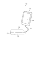
図1に示すように、超音波画像装置100は装置本体110と超音波プローブ130とを備える。装置本体110と超音波プローブ130とはケーブル120で接続され、装置本体110と超音波プローブ130の間でケーブル120を通じて電気信号のやり取りをすることができる。
そして、装置本体110には表示部112としてディスプレイパネルなどが組み込まれている。本実施形態では表示部112はタッチパネル型のディスプレイであり、ユーザーインターフェイス部(UI部)を兼ねている。
装置本体110では、超音波プローブ130で検出された超音波に基づき画像が生成され、画像化された検出結果が表示部112の画面に表示される。
超音波プローブ130は、直方体状の筐体132を備え、筐体132の長手方向の一端にケーブル120が接続されている。そして、その反対側に超音波の受発信を行うヘッド部134を有している。
なお、本実施形態の超音波画像装置100は、装置本体110と超音波プローブ130とをケーブル120で接続する形態であるが、ケーブル120を用いず、無線により装置本体110と超音波プローブ130との間で信号のやり取りを行う形態であっても良い。
As shown in FIG. 1, the
The apparatus
In the apparatus
The
In addition, although the
図2、図3に示すように、超音波プローブ130は、支持部材30に固定された超音波デバイス1が筐体132内に収容されている。超音波デバイス1の表面は筐体132のヘッド部134の表面で露出し、ヘッド部134の表面から対象物に対して超音波を出力するとともに、対象物からの超音波の反射波(エコー波)を受信することができる。
As shown in FIGS. 2 and 3, the
図3に示すように、超音波デバイス1と筐体132のヘッド部134との間には隙間があり、その隙間にはシリコーン系のシール材が充填されたシール部136が設けられている。このシール部136により、超音波プローブ130の筐体132の超音波デバイス1に水分などが侵入するのを防止している。
さらに、超音波デバイス1の支持部材30との間でシールするシール構造を有している。ここでのシール構造は、超音波デバイス1の支持部材30の外周部に貼り付けられた弾性を有する両面テープなどの接着部材35と、筐体132に貼り付けられた弾性を有する両面テープなどの接着部材135とを押し付ける状態で保持する構造である。
As shown in FIG. 3, there is a gap between the ultrasonic device 1 and the
Furthermore, it has a sealing structure for sealing with the
また、このシール部の一部には超音波デバイス1と処理回路とを接続するフレキシブル印刷配線基板(以下、FPC(Flexible Printed Circuits)と呼ぶことがある)60が介在し、この部分では、FPC60を接着部材35,135で挟んで押し付けられている。
なお、接着部材35,135としては、ポリエチレンまたはウレタンなどの単泡体にアクリル系の接着剤が塗布された両面テープが用いられている。
このように、本実施形態の超音波プローブ130では2重のシール構造が採用され、筐体132内に水分などが侵入するのを防止している。
In addition, a flexible printed wiring board (hereinafter also referred to as FPC (Flexible Printed Circuits)) 60 that connects the ultrasonic device 1 and the processing circuit is interposed in a part of the seal portion. In this part, the
In addition, as the
As described above, the
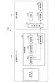
図4は超音波画像装置100の制御ブロック図である。
超音波画像装置100は、前述したように装置本体110と超音波プローブ130とを備える。
超音波プローブ130は、超音波デバイス1と処理回路150とを備えている。
処理回路150は、選択回路152、送信回路153、受信回路154、制御部155を有する。この処理回路150は、超音波デバイス1の送信処理及び受信処理を行う。
送信回路153は、送信期間において、選択回路152を介して超音波デバイス1に対して送信信号VTを出力する。具体的には、送信回路153は、制御部155の制御に基づいて送信信号VTを生成し、選択回路152に出力する。そして選択回路152は、制御部155の制御に基づいて、送信回路153からの送信信号VTを出力する。送信信号VTの周波数及び振幅電圧は、制御部155により設定することができる。
FIG. 4 is a control block diagram of the
As described above, the
The
The
The
受信回路154は、超音波デバイス1からの受信信号VRの受信処理を行う。具体的には、受信回路154は、受信期間において、選択回路152介して超音波デバイス1からの受信信号VRを受け取り、受信信号の増幅、ゲイン設定、周波数設定、A/D変換(アナログ/デジタル変換)などの受信処理を行う。受信処理の結果は、検出データ(検出情報)として装置本体110の処理部116に出力する。受信回路154は、例えば低雑音増幅器、電圧制御アッテネーター、プログラマブルゲインアンプ、ローパスフィルター、A/Dコンバーターなどで構成することができる。
制御部155は、送信回路153及び受信回路154を制御する。具体的には、制御部155は、送信回路153に対して送信信号VTの生成及び出力処理の制御を行い、受信回路154に対して受信信号VRの周波数設定やゲインなどの制御を行う。
選択回路152は、制御部155の制御に基づいて、選択された送信信号VTを出力する。
The
The
The
装置本体110は、表示部112、主制御部115、処理部116、UI部(ユーザーインターフェイス部)117、を含む。
主制御部115は、超音波プローブ130に対して超音波の送受信制御を行い、処理部116に対して検出データの画像処理等の制御を行う。
処理部116は、受信回路154からの検出データを受けて、必要な画像処理や表示用画像データの生成などを行う。
UI部117は、ユーザーの行う操作(例えばタッチパネル操作など)に基づいて主制御部115に必要な命令(コマンド)を出力する。
表示部112は、例えば液晶ディスプレイ等であって、処理部116からの表示用画像データを表示する。
なお、主制御部115が行う制御の一部を処理回路150の制御部155が行ってもよいし、制御部155が行う制御の一部を主制御部115が行ってもよい。
The apparatus
The
The
The
The
Note that a part of the control performed by the
(2)超音波デバイスの構成
次に、超音波プローブに組み込まれる超音波デバイスの構成について説明する。
図5は超音波デバイスの構成を示す平面図であり、図3における超音波プローブの矢印H方向から見た図に相当する。図6は図5のA−A断線に沿う断面図であり、図7は図5のB−B断線に沿う断面図である。
図5,6,7に示すように、超音波デバイス1は、超音波素子アレイ基板20、音響整合層40、音響レンズ50、フレキシブル配線基板(FPC)60を備えている。
(2) Configuration of Ultrasonic Device Next, the configuration of the ultrasonic device incorporated in the ultrasonic probe will be described.
FIG. 5 is a plan view showing the configuration of the ultrasonic device, and corresponds to a view of the ultrasonic probe seen from the direction of arrow H in FIG. 6 is a cross-sectional view taken along the line AA in FIG. 5, and FIG. 7 is a cross-sectional view taken along the line BB in FIG.
As shown in FIGS. 5, 6, and 7, the ultrasonic device 1 includes an ultrasonic
超音波素子アレイ基板20は、素子基板21とバックプレート22とを有している。
素子基板21は複数の超音波素子がアレイ状に配置された基板であり、平面視で長方形の形状をしている。この素子基板21はシリコン基板を用いて形成され、厚みがおよそ150μm〜200μmである。そして、素子基板21の素子形成面とは反対の面に、素子基板21と同じ平面形状に形成されたバックプレート22が接着されている。バックプレート22は素子基板21の余分な振動を抑える役目を果たし、およそ厚みが500μm〜600μmのシリコン基板が用いられている。このバックプレート22はシリコン基板の他に金属板を用いてもよい。
なお、場合によりバックプレート22を用いずに超音波デバイス1を構成してもよい。
超音波素子アレイ基板20の詳細については後述する。
The ultrasonic
The
In some cases, the ultrasonic device 1 may be configured without using the
Details of the ultrasonic
超音波素子アレイ基板20の超音波素子が形成されている面には、平面視で対向する長辺に沿って複数の超音波素子に接続される複数の端子(図示せず)が表出している。この端子とFPC60の端子(図示せず)とが接続され電気的接続が果たされている。
A plurality of terminals (not shown) connected to the plurality of ultrasonic elements are exposed along the long sides facing each other in plan view on the surface of the ultrasonic
超音波素子アレイ基板20の超音波素子が形成されている面の上には、平面形状が超音波素子アレイ基板20と同じである音響レンズ50が配置されている。音響レンズ50はシリコーン樹脂などの樹脂で形成されている。このシリコーン樹脂にはシリカなどを添加して比重を変えることで音響インピーダンスを調整することができる。
On the surface of the ultrasonic
超音波素子アレイ基板20と音響レンズ50の間には音響整合層40が形成されている。音響整合層40はシリコーン系の接着剤が用いられ、接着剤が硬化することで超音波素子アレイ基板20と音響レンズ50とを固着(接着)させ、硬化した接着剤(樹脂)が音響整合層として機能する。
An
音響レンズ50は、超音波素子アレイ基板20の超音波素子から発信される超音波を効率よく対象物に導き、また、対象物から反射して戻ってくるエコー波を効率よく超音波素子に導く役割を果たす。
音響整合層40は超音波素子と音響レンズ50の間の音響インピーダンスの不整合を緩和する役割を果たす。
The
The
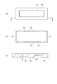
ここで、この音響レンズ50の構成を図8に示す。図8(a)は音響レンズ50の上面からの平面図であり、図8(b)はその裏面平面図である。図8(c)は同図(a)のC−C断線に沿う部分断面図であり、図8(d)は同図(a)のD−D断線に沿う部分断面図である。
Here, the configuration of the
音響レンズ50の一方の面に、所定の曲率で厚み方向に凸となるレンズ部51が設けられている。そして、その反対の面には音響レンズ50の外縁部に形成された厚み方向に突出する凸部としての壁部52が設けられている。
図8(b)に示すように、音響レンズ50の裏面に形成された壁部52は音響レンズ50の短辺の外縁部に設けられた壁部52aと、長辺の外縁部に設けられた壁部52bを備えている。また、音響レンズ50の四隅の部分には壁部が形成されていない。
図8(c)に示すように、壁部52aと壁部52bとは同じ厚みの基材から立ち上がり、壁の高さ寸法が異なるように構成されている。ここでは、壁部52aの方が壁部52bよりも壁の高さ寸法が長い。そして、この壁部の高さ寸法の差であるJ寸法は、FPC60の厚みと同じ寸法となっている。このように、対向する短辺の壁部52aは同じ高さ寸法に形成され、対向する長辺の壁部52bは同じ高さ寸法に形成されている。
また、図8(d)に示すように、壁部52aの基材からの高さ寸法であるK寸法は、音響整合層40の厚みと同じ寸法に設定されている。この音響整合層40の厚みは利用する超音波の波長λとして、例えば1/4λに設定されている。
なお、本実施形態では音響レンズ50の四隅の部分には壁部を形成しないが、壁部52aの高さ寸法より低い高さの壁部を設けてもよい。
また、音響レンズ50の超音波素子と対向する側に、耐湿性向上のためのポリイミドを熱圧着させた構造であっても良い。
さらに、音響レンズ50の超音波素子と対向する側に、第2の音響整合層を設けた構造であっても良い。
On one surface of the
As shown in FIG. 8B, the
As shown in FIG.8 (c), the
Further, as shown in FIG. 8D, the K dimension, which is the height dimension of the
In the present embodiment, no wall portion is formed at the four corners of the
Further, a structure in which polyimide for improving moisture resistance is thermocompression bonded to the side of the
Furthermore, the structure which provided the 2nd acoustic matching layer in the side facing the ultrasonic element of the
図5〜7に戻り、超音波素子アレイ基板20に音響レンズ50が固着された状態では、壁部52aが超音波素子アレイ基板20の表面に接触し(図6参照)、壁部52bがFPC60に接触する(図7参照)。
このように、FPC60を壁部52bで押さえ、超音波素子アレイ基板20とFPC60と接続部におけるFPC60の浮きを防止できる。
また、壁部52aの高さ寸法を設定することで超音波素子アレイ基板20の表面とレンズ部51との距離を簡単に設定することができ、その間に形成される音響整合層40の厚みを正確に設定することが可能である。
さらに、音響レンズ50の外縁部に壁部52a,52bが設けられ、FPC60の超音波素子アレイ基板20との接続位置は、音響レンズ50の外周より内側に配置されている。このため、音響レンズ50を超音波素子アレイ基板20上に安定して載置することができ、また、音響整合層40を形成する余分な接着剤は壁部52a,52bの間の隙間(音響レンズ50の四隅の部分)から流出し、音響レンズ50の浮きを防止し、かつ音響整合層40内に気泡が残存することを防止できる。なお、本実施形態では音響レンズ50の四隅の部分に壁部を形成しなかったが、特にこの部分でなくても他の部分に壁部を形成せずに、または壁部52aの高さ寸法より低い高さの壁部とすることで、接着剤を流動させる部分を形成してもよい。また、凸部として本実施形態では壁部を形成したが、複数の円柱などの柱部で凸部を形成しても良い。
また、FPC60の超音波素子アレイ基板20との接続位置は、音響レンズ50の外縁より内側に配置されているため、接続部が露出せず、音響整合層40でこの接続部を保護することができる。
5-7, in a state where the
In this manner, the
Moreover, the distance between the surface of the ultrasonic
Further,
Further, since the connection position of the
以上、上記の超音波デバイス1は、音響レンズ50の外縁部の少なくとも対向する2辺に音響レンズ50の厚み方向に突出する凸部としての壁部52が形成され、壁部52と超音波素子アレイ基板20の表面と接触している。
このことから、超音波素子アレイ基板20の表面と音響レンズ50のレンズ部51との距離が規定でき、超音波素子アレイ基板20と音響レンズ50との間に形成される音響整合層40の厚みを適正に設定することが容易である。そして、音響整合層40の厚みを精度よく形成することができるので、効率よく超音波を受発信することができる。
As described above, in the ultrasonic device 1, the
From this, the distance between the surface of the ultrasonic
(3)超音波素子および超音波素子アレイ基板
次に、本実施形態の超音波素子および超音波素子アレイ基板(素子基板)について、小型化を可能とする薄膜素子で構成した超音波素子を例にとって説明する。
図9は、本実施形態の超音波素子の概略平面図である。図10は、図9のE−E断線に沿った断面を示す概略断面図である。図11は本実施形態の超音波素子アレイ基板20の概略構成を示す説明図である。
(3) Ultrasonic Element and Ultrasonic Element Array Substrate Next, the ultrasonic element and the ultrasonic element array substrate (element substrate) of the present embodiment are examples of an ultrasonic element constituted by a thin film element that can be miniaturized. I will explain to you.
FIG. 9 is a schematic plan view of the ultrasonic element of the present embodiment. FIG. 10 is a schematic cross-sectional view showing a cross section taken along the line EE in FIG. FIG. 11 is an explanatory diagram showing a schematic configuration of the ultrasonic
図9、図10に示すように、超音波素子10は、ベース基板11と、ベース基板11に形成された振動膜(メンブレン)13と、振動膜13上に設けられた圧電体部18と、を有する。そして圧電体部18は、第1電極14、圧電体層15、第2電極16を有する。
As shown in FIGS. 9 and 10, the
超音波素子10は、シリコンなどのベース基板11に開口部12を有し、開口部12を覆って閉塞する振動膜13を備えている。
開口部12は、ベース基板11の裏面(素子が形成されない面)側から反応性イオンエッチング(RIE)等によりエッチングすることで形成される。
振動膜13は、例えばSiO2層とZrO2層との2層構造により構成される。ここで、SiO2層は、ベース基板11がSi基板である場合、基板表面を熱酸化処理することで成膜することができる。また、ZrO2層は、SiO2層上に例えばスパッタリングなどの手法により成膜される。ここで、ZrO2層は、後述する圧電体層15として例えばPZTを用いる場合に、PZTを構成するPbがSiO2層に拡散することを防止するための層である。また、ZrO2層は、圧電体層の歪みに対する撓み効率を向上させるなどの効果もある。
The
The
The
振動膜13の上には第1電極14が形成され、第1電極14の上に圧電体層15が形成され、さらに圧電体層15の上に第2電極16が形成されている。
つまり、第1電極14と第2電極16との間に圧電体層15が挟まれている構造となり、圧電体部18を構成している。
A
That is, the
第1電極14は、金属薄膜で形成され、複数の超音波素子を備える場合、図9のように素子形成領域の外側へ延長され、隣接する超音波素子に接続される配線であってもよい。
圧電体層15は、例えばPZT(ジルコン酸チタン酸鉛)薄膜により形成され、第1電極14の少なくとも一部を覆うように設けられる。なお、圧電体層15の材料は、PZTに限定されるものではなく、例えばチタン酸鉛(PbTiO3)、ジルコン酸鉛(PbZrO3)、チタン酸鉛ランタン((Pb、La)TiO3)などを用いてもよい。
第2電極16は、金属薄膜で形成され、圧電体層15の少なくとも一部を覆うように設けられる。この第2電極16は、複数の超音波素子を備える場合、図9のように素子形成領域の外側へ延長され、隣接する超音波素子に接続される配線であってもよい。
また、図10に示すように、超音波素子10を覆い、外部からの透湿を防止する防湿層19が備えられている。この防湿層19はアルミナなどの材料で形成され、超音波素子10の全面あるいは一部に設けられている。なお、この防湿層19は使用する状態や環境により適宜設ければよく、防湿層19を設けない構造であっても良い。
When the
The
The
Moreover, as shown in FIG. 10, the moisture-
圧電体層15は、第1電極14と第2電極16との間、即ち第1電極14と第2電極16との間に電圧が印加されることで、面内方向に伸縮する。従って、圧電体層15に電圧を印加すると、開口部12側に凸となる撓みが生じ、振動膜13を撓ませる。圧電体層15に交流電圧を印加することで、振動膜13が膜厚方向に対して振動し、この振動膜13の振動により超音波が開口部12から放射される。圧電体層15に印加される電圧(駆動電圧)は、例えばピークからピークで10〜30Vであり、周波数は例えば1〜10MHzである。
The
超音波素子10は、出射された超音波が対象物で反射されて戻ってくる超音波エコーを受信する受信素子としても動作する。超音波エコーにより振動膜13が振動し、この振動によって圧電体層15に応力が加わり、第1電極14と第2電極16との間に電圧が発生する。この電圧を受信信号として取り出すことができる。
The
上記の超音波素子10をアレイ状に配置した超音波素子アレイ基板について説明する。
図11に、本実施形態の超音波素子アレイ基板の構成を示す。
超音波素子アレイ基板20は、アレイ状に配置された複数の超音波素子10、駆動電極線DL、コモン電極線CLを含む。
複数の超音波素子10は、m行n列のマトリックス状に配置される。本実施形態では第1の方向D1に沿って8行、そして第1の方向D1に交差する第2の方向D2に沿って12列に配置される。
駆動電極線DL1〜DL12は、第1の方向D1に沿って配線される。
An ultrasonic element array substrate in which the
FIG. 11 shows the configuration of the ultrasonic element array substrate of the present embodiment.
The ultrasonic
The plurality of
The drive electrode lines DL1 to DL12 are wired along the first direction D1.
超音波を出射する送信期間には、前述した処理回路150が出力する送信信号VT1〜VT12が駆動電極線DL1〜DL12を介して各超音波素子10に供給される。また、超音波エコー信号を受信する受信期間には、超音波素子10からの受信信号VR1〜VR12が駆動電極線DL1〜DL12を介して処理回路150に出力される。
コモン電極線CL1〜CL8は、第2の方向D2に沿って配線される。
コモン電極線CL1〜CL8には、コモン電圧VCOMが供給される。このコモン電圧は一定の直流電圧であればよく、0V即ちグランド電位(接地電位)でなくてもよい。
In the transmission period in which the ultrasonic waves are emitted, the transmission signals VT1 to VT12 output from the
The common electrode lines CL1 to CL8 are wired along the second direction D2.
A common voltage VCOM is supplied to the common electrode lines CL1 to CL8. The common voltage may be a constant DC voltage, and may not be 0 V, that is, the ground potential (ground potential).
なお、超音波素子10の配置は、図11に示すm行n列のマトリックス配置に限定されない。
送信期間では、送信信号電圧とコモン電圧との差の電圧が各超音波素子10に印加され、所定の周波数の超音波が放射される。
The arrangement of the
In the transmission period, a difference voltage between the transmission signal voltage and the common voltage is applied to each
以上のように、本実施形態の超音波画像装置および超音波プローブは、効率よい超音波の受発信を行う超音波デバイス1を備えており、精度の高い超音波画像装置100および超音波プローブ130を提供できる。
(第2実施形態)
As described above, the ultrasonic imaging apparatus and the ultrasonic probe of the present embodiment include the ultrasonic device 1 that efficiently receives and transmits ultrasonic waves, and the
(Second Embodiment)
次に、第2実施形態として超音波デバイスの他の実施形態について説明する。本実施形態の超音波デバイスは超音波素子アレイ基板を収容する固定枠を備える点が第1実施形態で示した超音波デバイスと異なる。なお、第1実施形態と同様な構成については同符号を付し、説明を省略または簡略化する。
図12は超音波デバイスの構成を示す平面図であり、図13は超音波デバイスの音響レンズと音響整合層を取り外した状態を示す平面図である。図14は図12のE−E断線に沿う断面図であり、図15(a)は図12のF−F断線に沿う断面図であり、図15(b)は図12のG−G断線に沿う断面図である。
図12,13,14,15に示すように、超音波デバイス2は、超音波素子アレイ基板20、固定枠70、音響整合層40、音響レンズ80、フレキシブル配線基板(FPC)60を備えている。
Next, another embodiment of the ultrasonic device will be described as a second embodiment. The ultrasonic device of this embodiment is different from the ultrasonic device shown in the first embodiment in that it includes a fixed frame that accommodates an ultrasonic element array substrate. In addition, about the structure similar to 1st Embodiment, the same code | symbol is attached | subjected and description is abbreviate | omitted or simplified.
FIG. 12 is a plan view showing the configuration of the ultrasonic device, and FIG. 13 is a plan view showing a state where the acoustic lens and the acoustic matching layer of the ultrasonic device are removed. 14 is a sectional view taken along the line EE in FIG. 12, FIG. 15A is a sectional view taken along the line FF in FIG. 12, and FIG. 15B is a broken line GG in FIG. FIG.
As shown in FIGS. 12, 13, 14, and 15, the
超音波素子アレイ基板20は、第1実施形態と同じ構成であり素子基板21とバックプレート22とを有している。そして、超音波素子アレイ基板20は固定枠70に収容されている。
固定枠70は、平面部72と平面部72の外周に沿って立ち上がる枠部74とを備えている。平面部72には超音波素子アレイ基板20が接着剤などの接着層76により固定される。平面部72の外周から立ち上がる枠部74の上面は接着された超音波素子アレイ基板20の表面と同じ高さとなるように設定されている。なお、この固定枠70はアクリルなどの樹脂、または金属で形成されている。また、バックプレート22を用いずに直接固定枠70に素子基板21を接着した構成であってもよい。
The ultrasonic
The fixed
超音波素子アレイ基板20の超音波素子が形成されている面には、平面視で対向する長辺に沿って複数の超音波素子に接続される複数の端子(図示せず)が表出している。この端子とFPC60の端子(図示せず)とが接続され電気的接続が果たされている。
超音波素子アレイ基板20とFPC60とが接続された状態において、FPC60の固定枠70の枠部74の上面に対応する部分に、FPC60を貫通する穴部62が形成されている(図13参照)。
A plurality of terminals (not shown) connected to the plurality of ultrasonic elements are exposed along the long sides facing each other in plan view on the surface of the ultrasonic
In a state where the ultrasonic
超音波素子アレイ基板20の超音波素子が形成されている面の上には、平面形状が固定枠70と同じである音響レンズ80が配置されている。音響レンズ80はシリコーン樹脂などの樹脂で形成されている。このシリコーン樹脂にはシリカなどを添加して比重を変えることで音響インピーダンスを調整することができる。
On the surface of the ultrasonic
超音波素子アレイ基板20と音響レンズ80の間には音響整合層40が形成されている。音響整合層40はシリコーン系の接着剤が用いられ、接着剤が硬化することで超音波素子アレイ基板20と音響レンズ80とを固着(接着)させ、硬化した接着剤(樹脂)が音響整合層として機能する。
An
ここで、この音響レンズ80の構成を図16に示す。図16(a)は音響レンズ80の上面からの平面図であり、図16(b)はその裏面平面図である。図16(c)は同図(a)のP−P断線に沿う部分断面図である。
Here, the configuration of the
音響レンズ80の一方の面に、所定の曲率で厚み方向に凸となるレンズ部81が設けられている。そして、その反対の面には音響レンズ80の外縁部に形成された厚み方向に突出する凸部としての壁部82,83が設けられている。
図16(b)に示すように、音響レンズ80の裏面に形成された壁部82は音響レンズ80の短辺側の外縁部に設けられ、壁部83は長辺側の外縁部に設けられている。また、音響レンズ80の長辺側の一部には壁部が形成されていない。
On one surface of the
As shown in FIG. 16B, the
図16(c)に示すように、壁部82と壁部83とは同じ厚みの基材から立ち上がり、壁の高さ寸法が同じになるように構成されている。そして、壁部83には寸法Lだけ窪み、底面が平面である凹部84が形成されている。この寸法Lは前述したFPC60の厚みに相当する寸法である。壁部83に凹部84が形成されることで、壁部83の一部が突起状となり、この部分がFPC60の穴部62に間挿される。この壁部83の突起状の部分の平面形状はFPC60の穴部62と少し小さい寸法で形成され、FPC60を位置決めすることができる。
また、壁部82,83の高さ寸法Mは音響整合層40の厚みと同じ寸法に設定されている。なお、音響整合層40の厚みは利用する超音波の波長λとして、例えば1/4λに設定されている。
As shown in FIG.16 (c), the
Further, the height dimension M of the
図12〜15に戻り、超音波素子アレイ基板20に音響レンズ80が固着された状態では、壁部82,83の上面が固定枠70の枠部74上面と接触し(図14、図15(a)参照)、凹部84がFPC60に接触する(図15(b)参照)。
このように、壁部83をFPC60の穴部62に間挿することでFPC60を位置決めすることができ、凹部84はFPC60の厚みと同じ寸法で窪んでいるため、FPC60を固定枠70の枠部74との間に挟んで固定することができる。
また、壁部82,83の高さ寸法を設定することで超音波素子アレイ基板20の表面とレンズ部81との距離を簡単に設定することができ、その間に形成される音響整合層40の厚みを正確に設定することが可能である。
さらに、音響整合層40を形成する余分な接着剤は壁部を形成していない部分から流出し、音響レンズ80の浮きを防止し、かつ音響整合層40内に気泡が残存することを防止できる。
また、FPC60の超音波素子アレイ基板20との接続位置は、音響レンズ80の外縁より内側に配置されているため、接続部が露出せず、音響整合層40でこの接続部を保護することができる。
12 to 15, in the state where the
Thus, the
Moreover, the distance between the surface of the ultrasonic
Further, the excess adhesive forming the
Further, since the connection position of the
なお、本実施形態では音響レンズ80の壁部83の一部がFPC60を貫通して壁部83と固定枠70の枠部74上面と接触するように構成したが、壁部83をFPC60に接触させ、対向する短辺側に形成された壁部82のみを固定枠70の枠部74上面と接触するように構成してもよい。
In the present embodiment, a part of the
以上、上記の超音波デバイス2は、音響レンズ80の外縁部に厚み方向に突出する壁部82,83が形成され、壁部82,83と固定枠70の枠部74の上面と接触している。
このことから、超音波素子アレイ基板20の表面と音響レンズ80のレンズ部81との寸法が規定でき、超音波素子アレイ基板20と音響レンズ80との間に形成される音響整合層40の厚みを適正に設定することが容易である。そして、音響整合層40の厚みを精度よく形成することができるので、効率よく超音波を受発信することができる。
また、本実施形態では音響レンズ80は固定枠70と接触しており、素子基板21とは接触していない。このため、脆性材料で形成された素子基板21に不要な力が加わらない構造となっている。このため、超音波デバイス2を筐体などに組み込んで超音波プローブを構成した場合、超音波プローブが落下したときに素子基板を破損させることがなく、落下耐性を向上させることができる。
As described above, in the
Thus, the dimensions of the surface of the ultrasonic
In the present embodiment, the
(第2実施形態の変形例)
次に、第2実施形態における超音波デバイスの変形例について説明する。本変形例では、固定枠と音響レンズの構成が第2実施形態と異なる。
図17は超音波デバイスの変形例の構成を示す断面図である。第2実施形態と同様な構成要素については同符号を付し説明を省略する。
(Modification of the second embodiment)
Next, a modification of the ultrasonic device in the second embodiment will be described. In this modification, the configurations of the fixed frame and the acoustic lens are different from those of the second embodiment.
FIG. 17 is a cross-sectional view showing a configuration of a modification of the ultrasonic device. Constituent elements similar to those of the second embodiment are denoted by the same reference numerals and description thereof is omitted.
図17(a)に示すように、固定枠70aに超音波素子アレイ基板20が収容され、固定枠70aの枠部74aの上面は、超音波素子アレイ基板20の表面より高い位置に配置されている。枠部74aの上面は超音波素子アレイ基板20の表面から音響整合層40の厚み寸法だけ高い位置に設定されている。
As shown in FIG. 17A, the ultrasonic
音響レンズ80aの一方の面はレンズ部81aを備え、その反対側の面(枠部74aと対する面)は平面に形成されている。
そして、固定枠70aの枠部74a上面と音響レンズ80aとが接触することで、超音波素子アレイ基板20の表面とレンズ部81aとの間の寸法が規定でき、超音波素子アレイ基板20と音響レンズ80aとの間に形成される音響整合層40の厚みを適正に設定することが容易である。
One surface of the
Then, when the upper surface of the
図17(b)に示すように、固定枠70bに超音波素子アレイ基板20が収容され、固定枠70bの枠部74bの上面は、超音波素子アレイ基板20の表面より低い位置に配置されている。
音響レンズ80bの一方の面はレンズ部81bを備え、その反対側の面(枠部74bと対する面)の外周縁には壁部82bが形成されている。壁部82bの高さ寸法は、固定枠70bの枠部74b上面と音響レンズ80bの壁部82bとが接触したときに、超音波素子アレイ基板20とレンズ部81bとの寸法が音響整合層40の厚みとなるように設定されている。
このようにすれば、超音波素子アレイ基板20の表面とレンズ部81bとの間の寸法が規定でき、超音波素子アレイ基板20と音響レンズ80bとの間に形成される音響整合層40の厚みを適正に設定することが容易である。
As illustrated in FIG. 17B, the ultrasonic
One surface of the
In this way, the dimension between the surface of the ultrasonic
以上、上記で説明した超音波デバイス2,3,4を搭載して、超音波プローブを構成してもよく、さらに超音波画像装置などの電子機器を構成してもよい。
As described above, the
次に、上記第1実施形態では携帯型の超音波画像装置を示したが、図18に、他の実施形態の超音波画像装置の具体的な構成例を示す。
超音波画像装置101は据置型の超音波画像装置であり、超音波プローブ130を備えている。
超音波画像装置101は、装置本体(電子機器本体)111、表示用画像データを表示する表示部113、ユーザーインターフェイス部(UI部)117、超音波プローブ130、ケーブル120を有している。
このような据置型の超音波画像装置であっても、本発明の効果を奏することができる。
また、本実施形態の超音波画像装置は、生体の脂肪厚み、筋肉厚み、血流、骨密度などの測定に利用することができる。
Next, although the portable ultrasonic imaging apparatus is shown in the first embodiment, FIG. 18 shows a specific configuration example of the ultrasonic imaging apparatus according to another embodiment.
The
The
Even with such a stationary ultrasonic imaging apparatus, the effects of the present invention can be achieved.
Moreover, the ultrasonic imaging apparatus of this embodiment can be used for measurement of fat thickness, muscle thickness, blood flow, bone density, and the like of a living body.
本発明は以上説明した実施形態に限定されるものではなく、本発明の実施の際の具体的な構造および手順は、本発明の目的を達成できる範囲で他の構造などに適宜変更することができる。そして、多くの変形が本発明の技術的思想内で当分野において通常の知識を有するものにより可能である。 The present invention is not limited to the embodiment described above, and the specific structure and procedure for carrying out the present invention can be appropriately changed to other structures and the like as long as the object of the present invention can be achieved. it can. Many modifications can be made by those skilled in the art within the technical idea of the present invention.
1,2,3,4…超音波デバイス、10…超音波素子、11…ベース基板、12…開口部、13…振動膜、14…第1電極、15…圧電体層、16…第2電極、18…圧電体部、19…防湿層、20…超音波素子アレイ基板、21…素子基板、22…バックプレート、30…支持部材、35…接着部材、40…音響整合層、50…音響レンズ、51…レンズ部、52,52a,52b…壁部(凸部)、60…フレキシブル印刷配線基板(FPC)、62…穴部、65…接着部、70…固定枠、72…平面部、74…枠部、76…接着層、70a,70b…固定枠、74a,74b…枠部、80…音響レンズ、81…レンズ部、82,83…壁部(凸部)、84…凹部、80a,80b…音響レンズ、81a,81b…レンズ部、82b…壁部、100,101…超音波画像装置、110…装置本体、112,113…表示部、115…主制御部、116…処理部、117…ユーザーインターフェイス部(UI部)、120…ケーブル、130…超音波プローブ、132…筐体、134…ヘッド部、135…接着部材、136…シール部、150…処理回路、152…選択回路、153…送信回路、154…受信回路、155…制御部。
DESCRIPTION OF
Claims (17)
前記超音波素子基板の前記超音波素子が形成された面に固着され超音波を収束させるレンズ部を有する音響レンズと、
前記超音波素子基板と前記音響レンズの間に配置され、前記超音波素子基板と前記音響レンズとを固着する樹脂で形成された音響整合層と、を備え、
前記音響レンズの前記超音波素子基板の前記超音波素子と対向する面において、
前記音響レンズに、前記音響レンズの厚み方向に突出する複数の凸部が形成され、
前記複数の凸部のうちの少なくとも2つが、前記超音波素子基板の厚み方向の平面視において、前記超音波素子基板と接触し、
前記複数の凸部と前記超音波素子基板とが接触する位置は、前記超音波素子の形成されていない外周部の対向する2辺である
ことを特徴とする超音波デバイス。 An ultrasonic element substrate having an ultrasonic element that includes a piezoelectric body and performs at least one of transmission and reception of ultrasonic waves;
An acoustic lens having a lens portion that is fixed to the surface of the ultrasonic element substrate on which the ultrasonic element is formed and focuses the ultrasonic wave;
An acoustic matching layer that is disposed between the ultrasonic element substrate and the acoustic lens and formed of a resin that fixes the ultrasonic element substrate and the acoustic lens; and
In the surface facing the ultrasonic element of the ultrasonic element substrate of the acoustic lens,
A plurality of convex portions protruding in the thickness direction of the acoustic lens are formed on the acoustic lens,
Wherein the plurality of at least two of the convex portion, the in plan view in the thickness direction of the ultrasonic element substrate, in contact with the ultrasonic element board,
The ultrasonic device, wherein the plurality of convex portions and the ultrasonic element substrate are in contact with each other on two opposing sides of the outer peripheral portion where the ultrasonic element is not formed .
前記音響整合層は前記超音波素子基板と前記音響レンズとの間に充填され、前記超音波素子基板と前記音響レンズとに固着している樹脂である
ことを特徴とする超音波デバイス。 The ultrasonic device according to claim 1,
The ultrasonic device, wherein the acoustic matching layer is a resin that is filled between the ultrasonic element substrate and the acoustic lens and is fixed to the ultrasonic element substrate and the acoustic lens.
前記複数の凸部の一部に、前記音響レンズの厚み方向に突出する寸法の異なる部分を有する
ことを特徴とする超音波デバイス。 The ultrasonic device according to claim 2,
The ultrasonic device according to claim 1, wherein a part of the plurality of convex portions includes a portion having a different size protruding in a thickness direction of the acoustic lens.
前記超音波素子基板の前記超音波素子が形成された面にて接続するフレキシブル印刷配線基板を備え、
前記フレキシブル印刷配線基板は前記超音波素子基板に電気的に接続し、
前記音響レンズの前記複数の凸部の一部は前記フレキシブル印刷配線基板と接触してる
ことを特徴とする超音波デバイス。 The ultrasonic device according to any one of claims 1 to 3,
A flexible printed wiring board connected on the surface of the ultrasonic element substrate on which the ultrasonic element is formed;
The flexible printed wiring board is electrically connected to the ultrasonic element substrate,
The ultrasonic device, wherein a part of the plurality of convex portions of the acoustic lens is in contact with the flexible printed wiring board.
前記超音波素子基板は、
開口部が形成されたベース基板と、
前記開口部を覆って形成され膜厚方向に変位可能な振動膜と、
前記振動膜に設けられた圧電体部と、を有し、
前記圧電体部は、
前記振動膜の上に設けられる第1電極と、
前記第1電極の少なくとも一部を覆って設けられる圧電体層と、
前記圧電体層の少なくとも一部を覆って設けられる第2電極と、を有する
ことを特徴とする超音波デバイス。 In the ultrasonic device according to any one of claims 1 to 4,
The ultrasonic element substrate is
A base substrate having an opening formed thereon;
A vibrating membrane formed over the opening and displaceable in the film thickness direction;
A piezoelectric body portion provided on the vibration film,
The piezoelectric part is
A first electrode provided on the vibrating membrane;
A piezoelectric layer provided to cover at least a part of the first electrode;
An ultrasonic device comprising: a second electrode provided to cover at least a part of the piezoelectric layer.
前記超音波デバイスを支持する筐体と、を備えることを特徴とする超音波プローブ。 The ultrasonic device according to any one of claims 1 to 5,
An ultrasonic probe comprising: a housing that supports the ultrasonic device.
前記超音波デバイスに接続され、前記超音波デバイスの出力を処理する処理回路と、
を備えることを特徴とする電子機器。 The ultrasonic device according to any one of claims 1 to 5,
A processing circuit connected to the ultrasonic device and processing an output of the ultrasonic device;
An electronic device comprising:
前記超音波デバイスに接続され、前記超音波デバイスの出力を処理し画像を生成する処理回路と、
前記画像を表示する表示部と、
を備えることを特徴とする超音波画像装置。 The ultrasonic device according to any one of claims 1 to 5,
A processing circuit connected to the ultrasonic device and processing the output of the ultrasonic device to generate an image;
A display unit for displaying the image;
An ultrasonic imaging apparatus comprising:
前記超音波素子基板が固着される平面部と前記平面部の周りに立設された枠部とを有する固定枠と、
前記固定枠の前記枠部の上面と固着され超音波を収束させるレンズ部を有する音響レンズと、を備え、
前記音響レンズと前記固定枠の前記枠部の少なくとも対向する2辺の前記上面とが接触する
ことを特徴とする超音波デバイス。 An ultrasonic element substrate having an ultrasonic element that includes a piezoelectric body and performs at least one of transmission and reception of ultrasonic waves;
A fixed frame having a flat part to which the ultrasonic element substrate is fixed and a frame part standing around the flat part;
An acoustic lens having a lens portion that is fixed to the upper surface of the frame portion of the fixed frame and converges ultrasonic waves, and
Ultrasonic devices and the upper surface of the two sides at least facing the frame portion of the fixed frame and the acoustic lens is characterized in that you contact.
前記超音波素子基板と前記音響レンズとの間に設けられた音響整合層を備え、
前記音響整合層は前記超音波素子基板と前記音響レンズとに固着している樹脂で形成されている
ことを特徴とする超音波デバイス。 The ultrasonic device according to claim 9.
An acoustic matching layer provided between the ultrasonic element substrate and the acoustic lens;
The acoustic device is characterized in that the acoustic matching layer is formed of a resin fixed to the ultrasonic element substrate and the acoustic lens.
前記音響レンズの前記超音波素子基板と対向する面において、
前記音響レンズの外縁部に、前記音響レンズの厚み方向に突出する複数の凸部が形成されている
ことを特徴とする超音波デバイス。 The ultrasonic device according to claim 9 or 10,
On the surface of the acoustic lens facing the ultrasonic element substrate,
A plurality of convex portions protruding in a thickness direction of the acoustic lens are formed on an outer edge portion of the acoustic lens.
前記複数の凸部の一部に、前記音響レンズの厚み方向に突出する寸法の異なる部分を有する
ことを特徴とする超音波デバイス。 The ultrasonic device according to claim 11.
The ultrasonic device according to claim 1, wherein a part of the plurality of convex portions includes a portion having a different size protruding in a thickness direction of the acoustic lens.
前記超音波素子基板の前記超音波素子が形成された面にて前記超音波素子基板に電気的に接続するフレキシブル印刷配線基板を備え、
前記フレキシブル印刷配線基板は前記固定枠の前記枠部の前記上面と対応する部分に穴部が形成され、
前記音響レンズの前記複数の凸部の一部に前記フレキシブル印刷配線基板の厚みと同じ寸法で窪んだ凹部が形成され、
前記音響レンズの前記複数の凸部の一部が前記フレキシブル印刷配線基板の前記穴部に間挿されて前記固定枠の前記枠部の上面が接触し、前記凹部が前記フレキシブル印刷配線基板と接触している
ことを特徴とする超音波デバイス。 The ultrasonic device according to claim 11 or 12,
A flexible printed wiring board electrically connected to the ultrasonic element substrate at a surface of the ultrasonic element substrate on which the ultrasonic element is formed;
The flexible printed wiring board has a hole formed in a portion corresponding to the upper surface of the frame portion of the fixed frame,
Recesses that are recessed with the same dimensions as the thickness of the flexible printed wiring board are formed in some of the plurality of convex portions of the acoustic lens,
A part of the plurality of convex portions of the acoustic lens is inserted into the hole portion of the flexible printed wiring board, the upper surface of the frame portion of the fixed frame is in contact, and the concave portion is in contact with the flexible printed wiring board. An ultrasonic device characterized by that.
前記超音波素子基板は、
開口部が形成されたベース基板と、
個々の前記開口部を覆って形成され膜厚方向に変位可能な振動膜と、
個々の前記振動膜に設けられた圧電体部と、を有し、
前記圧電体部は、
前記振動膜の上に設けられる第1電極と、
前記第1電極の少なくとも一部を覆って設けられる圧電体層と、
前記圧電体層の少なくとも一部を覆って設けられる第2電極と、を有する
ことを特徴とする超音波デバイス。 The ultrasonic device according to any one of claims 9 to 13,
The ultrasonic element substrate is
A base substrate having an opening formed thereon;
A vibrating membrane formed to cover each of the openings and displaceable in the film thickness direction;
A piezoelectric body portion provided on each of the vibrating membranes,
The piezoelectric part is
A first electrode provided on the vibrating membrane;
A piezoelectric layer provided to cover at least a part of the first electrode;
An ultrasonic device comprising: a second electrode provided to cover at least a part of the piezoelectric layer.
前記超音波デバイスを支持する筐体と、を備えることを特徴とする超音波プローブ。 The ultrasonic device according to any one of claims 9 to 14,
An ultrasonic probe comprising: a housing that supports the ultrasonic device.
前記超音波デバイスに接続され、前記超音波デバイスの出力を処理する処理回路と、
を備えることを特徴とする電子機器。 The ultrasonic device according to any one of claims 9 to 14,
A processing circuit connected to the ultrasonic device and processing an output of the ultrasonic device;
An electronic device comprising:
前記超音波デバイスに接続され、前記超音波デバイスの出力を処理し画像を生成する処理回路と、
前記画像を表示する表示部と、
を備えることを特徴とする超音波画像装置。 The ultrasonic device according to any one of claims 9 to 14,
A processing circuit connected to the ultrasonic device and processing the output of the ultrasonic device to generate an image;
A display unit for displaying the image;
An ultrasonic imaging apparatus comprising:
Priority Applications (1)
| Application Number | Priority Date | Filing Date | Title |
|---|---|---|---|
| JP2013012948A JP6175779B2 (en) | 2013-01-28 | 2013-01-28 | Ultrasonic device, ultrasonic probe, electronic device and ultrasonic imaging apparatus |
Applications Claiming Priority (1)
| Application Number | Priority Date | Filing Date | Title |
|---|---|---|---|
| JP2013012948A JP6175779B2 (en) | 2013-01-28 | 2013-01-28 | Ultrasonic device, ultrasonic probe, electronic device and ultrasonic imaging apparatus |
Publications (3)
| Publication Number | Publication Date |
|---|---|
| JP2014146884A JP2014146884A (en) | 2014-08-14 |
| JP2014146884A5 JP2014146884A5 (en) | 2016-03-10 |
| JP6175779B2 true JP6175779B2 (en) | 2017-08-09 |
Family
ID=51426818
Family Applications (1)
| Application Number | Title | Priority Date | Filing Date |
|---|---|---|---|
| JP2013012948A Active JP6175779B2 (en) | 2013-01-28 | 2013-01-28 | Ultrasonic device, ultrasonic probe, electronic device and ultrasonic imaging apparatus |
Country Status (1)
| Country | Link |
|---|---|
| JP (1) | JP6175779B2 (en) |
Families Citing this family (5)
| Publication number | Priority date | Publication date | Assignee | Title |
|---|---|---|---|---|
| JP6331396B2 (en) | 2014-01-06 | 2018-05-30 | セイコーエプソン株式会社 | Ultrasonic device, ultrasonic probe, electronic apparatus, and manufacturing method of ultrasonic device |
| JP6402983B2 (en) | 2014-08-29 | 2018-10-10 | セイコーエプソン株式会社 | Ultrasonic device, method for manufacturing ultrasonic device, ultrasonic probe, ultrasonic measuring device, electronic equipment |
| CN108135574A (en) * | 2015-10-29 | 2018-06-08 | 阿文特公司 | Ultrasonic probe with integrated needle propeller |
| JP7396071B2 (en) | 2020-01-23 | 2023-12-12 | セイコーエプソン株式会社 | ultrasound device |
| WO2023116927A1 (en) * | 2021-12-24 | 2023-06-29 | 深圳市影越医疗科技有限公司 | Phonophoresis structure, elasticity measurement apparatus, probe, system, and method |
Family Cites Families (6)
| Publication number | Priority date | Publication date | Assignee | Title |
|---|---|---|---|---|
| JPS60128795A (en) * | 1983-12-16 | 1985-07-09 | Toshiba Corp | Ultrasonic probe |
| JPS61146240A (en) * | 1984-12-19 | 1986-07-03 | 松下電器産業株式会社 | Ultrasonic doppler probe |
| JPH07106201B2 (en) * | 1989-02-01 | 1995-11-15 | アロカ株式会社 | Ultrasonic probe |
| JPH0678398A (en) * | 1992-08-27 | 1994-03-18 | Toshiba Ceramics Co Ltd | Ultrasonic wave transducer |
| JP4633571B2 (en) * | 2005-07-28 | 2011-02-16 | オリンパスメディカルシステムズ株式会社 | Array type ultrasonic transducer and manufacturing method thereof |
| JP2011082624A (en) * | 2009-10-02 | 2011-04-21 | Asahi Kasei Electronics Co Ltd | Proximity ultrasonic sensor |
-
2013
- 2013-01-28 JP JP2013012948A patent/JP6175779B2/en active Active
Also Published As
| Publication number | Publication date |
|---|---|
| JP2014146884A (en) | 2014-08-14 |
Similar Documents
| Publication | Publication Date | Title |
|---|---|---|
| JP6212870B2 (en) | Ultrasonic device, ultrasonic probe, electronic device and ultrasonic imaging apparatus | |
| JP6175780B2 (en) | Ultrasonic device, ultrasonic probe, electronic device and ultrasonic imaging apparatus | |
| JP6229431B2 (en) | Ultrasonic device, ultrasonic probe head, ultrasonic probe, electronic device and ultrasonic imaging apparatus | |
| JP6135088B2 (en) | Ultrasonic transducer device, probe head, ultrasonic probe, electronic device and ultrasonic diagnostic apparatus | |
| US10085720B2 (en) | Ultrasonic device, method for producing ultrasonic device, ultrasonic probe, ultrasonic measurement apparatus, and electronic device | |
| JP6175779B2 (en) | Ultrasonic device, ultrasonic probe, electronic device and ultrasonic imaging apparatus | |
| JP6252280B2 (en) | Ultrasonic device unit and probe, electronic apparatus and ultrasonic imaging apparatus | |
| US10350639B2 (en) | Ultrasonic device, piezoelectric device, ultrasonic measurement apparatus, and electronic instrument | |
| JP6326833B2 (en) | Ultrasonic device, method for manufacturing ultrasonic device, probe, electronic device, ultrasonic imaging apparatus | |
| CN105559821B (en) | Ultrasonic probe, electronic device, and ultrasonic imaging apparatus | |
| CN108282729B (en) | Ultrasonic device, ultrasonic probe, and ultrasonic apparatus | |
| JP2015097734A (en) | Ultrasound device and method of producing the same and electronic apparatus and ultrasonic image device | |
| JP6248535B2 (en) | Ultrasonic device, ultrasonic probe head, ultrasonic probe, electronic apparatus, ultrasonic imaging apparatus, and method of manufacturing ultrasonic device | |
| US20160031128A1 (en) | Method for manufacturing acoustic coupling member | |
| CN114550684A (en) | Piezoelectric actuator, ultrasonic element, ultrasonic device, and electronic apparatus | |
| WO2022210887A1 (en) | Ultrasonic probe head, ultrasonic probe, and ultrasonic diagnostic apparatus | |
| WO2022210851A1 (en) | Flexible ultrasonic probe head, ultrasonic probe, and ultrasonic diagnostic device | |
| JP2018114042A (en) | Ultrasound probe, ultrasound diagnostic apparatus, and semiconductor sensor | |
| JP6451216B2 (en) | Ultrasonic probe, electronic device and ultrasonic imaging device | |
| CN114504344A (en) | Piezoelectric actuator, ultrasonic element, ultrasonic probe, and ultrasonic device |
Legal Events
| Date | Code | Title | Description |
|---|---|---|---|
| RD04 | Notification of resignation of power of attorney |
Free format text: JAPANESE INTERMEDIATE CODE: A7424 Effective date: 20150109 |
|
| A521 | Written amendment |
Free format text: JAPANESE INTERMEDIATE CODE: A523 Effective date: 20160121 |
|
| A621 | Written request for application examination |
Free format text: JAPANESE INTERMEDIATE CODE: A621 Effective date: 20160121 |
|
| RD04 | Notification of resignation of power of attorney |
Free format text: JAPANESE INTERMEDIATE CODE: A7424 Effective date: 20160610 |
|
| RD03 | Notification of appointment of power of attorney |
Free format text: JAPANESE INTERMEDIATE CODE: A7423 Effective date: 20160624 |
|
| A977 | Report on retrieval |
Free format text: JAPANESE INTERMEDIATE CODE: A971007 Effective date: 20161114 |
|
| A131 | Notification of reasons for refusal |
Free format text: JAPANESE INTERMEDIATE CODE: A131 Effective date: 20161206 |
|
| A521 | Written amendment |
Free format text: JAPANESE INTERMEDIATE CODE: A523 Effective date: 20170131 |
|
| TRDD | Decision of grant or rejection written | ||
| A01 | Written decision to grant a patent or to grant a registration (utility model) |
Free format text: JAPANESE INTERMEDIATE CODE: A01 Effective date: 20170613 |
|
| A61 | First payment of annual fees (during grant procedure) |
Free format text: JAPANESE INTERMEDIATE CODE: A61 Effective date: 20170626 |
|
| R150 | Certificate of patent or registration of utility model |
Ref document number: 6175779 Country of ref document: JP Free format text: JAPANESE INTERMEDIATE CODE: R150 |