JP6167520B2 - Device manufacturing method - Google Patents
Device manufacturing method Download PDFInfo
- Publication number
- JP6167520B2 JP6167520B2 JP2013000895A JP2013000895A JP6167520B2 JP 6167520 B2 JP6167520 B2 JP 6167520B2 JP 2013000895 A JP2013000895 A JP 2013000895A JP 2013000895 A JP2013000895 A JP 2013000895A JP 6167520 B2 JP6167520 B2 JP 6167520B2
- Authority
- JP
- Japan
- Prior art keywords
- etching
- substrate
- vibration element
- hydrofluoric acid
- exposed
- Prior art date
- Legal status (The legal status is an assumption and is not a legal conclusion. Google has not performed a legal analysis and makes no representation as to the accuracy of the status listed.)
- Active
Links
Images


Description
本発明は、水晶板を用いた素子の製造方法に関する。 The present invention relates to a method for manufacturing an element using a quartz plate.
素子の一例としてのATカット水晶振動素子を用いた水晶振動素子は、その振動モードが厚みすべり振動であり、且つ周波数温度特性が優れた三次曲線を呈するので、電子機器等の多方面で使用されている。特許文献1には、エネルギー閉じ込め効果がベベル構造やコンベックス構造と同程度の効果を有する、所謂メサ型構造の振動素子(ATカット水晶振動素子)が開示されている。また、メサ型構造の振動素子の外形形成には、フッ化水素(HF)を含む溶液によるエッチング加工が用いられていることが開示されている。
A crystal resonator element using an AT-cut crystal resonator element as an example of the element has a vibration mode of thickness shear vibration and exhibits a cubic curve with excellent frequency temperature characteristics, so it is used in various fields such as electronic equipment. ing.
しかしながら、上述した振動素子の外形形成方法では、フッ化水素(HF)を含む溶液によるエッチング加工によって水晶板をエッチングし、段状のメサ型構造を形成する際に、既に外形加工がなされ、交差して露出する水晶板の2面が、再度フッ化水素(HF)を含む溶液に晒され、さらにエッチングが進んでしまう。同様に、多段のメサ型構造では、2段目のメサ型構造を形成する際に、既に加工がなされたメサ型構造部分の、交差して露出する2面が再度フッ化水素(HF)を含む溶液に晒され、さらにエッチングが進んでしまう。これにより、再度フッ化水素(HF)を含む溶液に晒された、交差して露出する2面の交差部分が侵食され、形状が安定しない、所謂形状ばらつきを生じてしまう。この形状のばらつきが生じることにより、エネルギー閉じ込め効果がばらつき、振動素子の電気的特性、特に、発振のし易さの目安となるCI(Crystal Impedance)値の劣化、ばらつきを生じてしまう虞があった。 However, in the above-described method for forming the outer shape of the vibration element, when the crystal plate is etched by etching with a solution containing hydrogen fluoride (HF) to form a stepped mesa structure, the outer shape has already been formed, Then, the two exposed quartz plates are again exposed to a solution containing hydrogen fluoride (HF), and etching proceeds further. Similarly, in the case of a multi-stage mesa structure, when forming a second-stage mesa structure, the two exposed surfaces of the mesa structure that have already been processed are exposed again to hydrogen fluoride (HF). Etching progresses further due to exposure to the solution. As a result, the intersecting portion of the two surfaces exposed to intersect with each other exposed again to the solution containing hydrogen fluoride (HF) is eroded, and so-called shape variation in which the shape is not stable is generated. Due to this variation in shape, there is a risk that the energy confinement effect will vary, and the electrical characteristics of the vibration element, especially the CI (Crystal Impedance) value, which is a measure of the ease of oscillation, will deteriorate and vary. It was.
本発明は、上述の課題の少なくとも一部を解決するためになされたものであり、以下の形態または適用例として実現することが可能である。 SUMMARY An advantage of some aspects of the invention is to solve at least a part of the problems described above, and the invention can be implemented as the following forms or application examples.
[適用例1]本適用例に係る素子の製造方法は、凸部を有する水晶板を準備する工程と、HFを含み、温度が25℃以上55℃以下の範囲にあるエッチング液を用いて、前記凸部の表面をエッチングする工程と、を含むことを特徴とする。 [Application Example 1] A method of manufacturing an element according to this application example includes a step of preparing a crystal plate having a convex portion, and an etching solution containing HF and having a temperature in the range of 25 ° C. to 55 ° C. And a step of etching the surface of the convex portion.
本適用例によれば、交差して露出する2面によって構成された凸部を含む水晶板のエッチング加工に、温度が25℃以上50℃以下のHF(フッ化水素)を含む溶液を用いる。これにより、交差して露出する水晶板の2面の交差部分の侵食が抑えられ、交差して露出する2面の交差部分の形状が安定する。その結果、エネルギー閉じ込め効果のばらつきが小さくなり、振動素子の電気的特性、特にCI値の劣化、ばらつきを防止することが可能となる。 According to this application example, a solution containing HF (hydrogen fluoride) having a temperature of 25 ° C. or more and 50 ° C. or less is used for etching processing of a crystal plate including a convex portion constituted by two surfaces exposed to intersect each other. As a result, the erosion of the intersecting portions of the two surfaces of the quartz plate exposed by crossing is suppressed, and the shape of the intersecting portions of the two surfaces exposed by intersecting is stabilized. As a result, the variation in the energy confinement effect is reduced, and it becomes possible to prevent deterioration and variation in the electrical characteristics of the vibration element, particularly the CI value.
[適用例2]上記適用例に記載の素子の製造方法において、前記エッチング液は、NH4FHF、またはNH4HF2とHFとの混合液を含むことが好ましい。 Application Example 2 In the device manufacturing method described in the application example, it is preferable that the etching solution includes NH 4 FHF or a mixed solution of NH 4 HF 2 and HF.
本適用例によれば、このようなエッチング液を用いることで、エッチング加工を容易に、形状ばらつきを小さく行うことが可能となる。 According to this application example, by using such an etching solution, it is possible to easily perform etching processing and reduce the shape variation.
[適用例3]上記適用例に記載の素子の製造方法において、前記エッチング液の温度が、30℃以上38℃以下の範囲にあることが好ましい。 Application Example 3 In the device manufacturing method described in the application example, it is preferable that the temperature of the etching solution is in a range of 30 ° C. or more and 38 ° C. or less.
本適用例によれば、エッチング速度、侵食の進み具合から、特に好適にエッチング加工を行うことができる。 According to this application example, the etching process can be performed particularly preferably from the etching rate and the progress of erosion.
[適用例4]上記適用例に記載の素子の製造方法において、前記NH4HF2とHFとの混合液は、HFに対するNH4HF2の重量比が1.5以上2.5以下の範囲であることが好ましい。 Application Example 4 In the device manufacturing method according to the application example described above, the mixed solution of NH 4 HF 2 and HF has a weight ratio of NH 4 HF 2 to HF in the range of 1.5 to 2.5. It is preferable that
本適用例によれば、このようなエッチング液を用いることで、エッチング加工を容易に、形状ばらつきを小さく行うことが可能となる。 According to this application example, by using such an etching solution, it is possible to easily perform etching processing and reduce the shape variation.
[適用例5]上記適用例に記載の素子の製造方法において、前記凸部は、前記水晶板の外形端面を含むことが好ましい。 Application Example 5 In the element manufacturing method according to the application example described above, it is preferable that the convex portion includes an outer end face of the crystal plate.
本適用例によれば、素子の外形端面の形状が安定するため、素子の位置決め精度の向上などを図ることが可能となる。さらに、素子の電気的特性の向上も図ることができる。 According to this application example, since the shape of the outer end face of the element is stabilized, it is possible to improve the positioning accuracy of the element. Furthermore, the electrical characteristics of the element can be improved.
[適用例6]上記適用例に記載の素子の製造方法において、前記水晶板は、ATカット板であることが好ましい。 Application Example 6 In the device manufacturing method described in the application example, it is preferable that the crystal plate is an AT cut plate.
本適用例によれば、電気的特性の安定したメサ型構造のATカット振動素子を提供することが可能となる。 According to this application example, it is possible to provide an AT-cut vibration element having a mesa structure with stable electrical characteristics.
[適用例7]上記適用例に記載の素子の製造方法において、前記水晶板は、メサ形状を有し、前記凸部は、前記メサ形状の段部を構成していることが好ましい。 Application Example 7 In the element manufacturing method according to the application example described above, it is preferable that the crystal plate has a mesa shape and the convex portion constitutes the mesa-shaped stepped portion.
本適用例によれば、凸部を構成しているメサ形状の段部において、露出して交差する2面の交差部分の侵食が抑えられ、交差して露出する2面の交差部分の形状が安定する。その結果、エネルギー閉じ込め効果のばらつきが小さくなり、振動素子の電気的特性、特にCI値の劣化、ばらつきを防止することが可能となる。 According to this application example, in the mesa-shaped step portion constituting the convex portion, the erosion of the intersecting portion of the two surfaces that are exposed and intersecting is suppressed, and the shape of the intersecting portion of the two surfaces that are exposed to intersect is the shape. Stabilize. As a result, the variation in the energy confinement effect is reduced, and it becomes possible to prevent deterioration and variation in the electrical characteristics of the vibration element, particularly the CI value.
[適用例8]上記適用例に記載の素子の製造方法において、前記メサ形状は、順メサ形状であることが好ましい。 Application Example 8 In the device manufacturing method according to the application example described above, the mesa shape is preferably a forward mesa shape.
本適用例によれば、凸部を構成している順メサ形状の段部において、交差して露出する2面の交差部分の侵食が抑えられ、交差して露出する2面の交差部分の形状が安定する。その結果、エネルギー閉じ込め効果のばらつきが小さくなり、振動素子の電気的特性、特にCI値の劣化、ばらつきを防止することが可能となる。 According to this application example, in the forward mesa-shaped stepped portion constituting the convex portion, the erosion of the intersecting portion of the two surfaces exposed to intersect is suppressed, and the shape of the intersecting portion of the two surfaces exposed to intersect Is stable. As a result, the variation in the energy confinement effect is reduced, and it becomes possible to prevent deterioration and variation in the electrical characteristics of the vibration element, particularly the CI value.
[適用例9]上記適用例に記載の素子の製造方法において、前記メサ形状は、多段メサ形状の少なくとも一部であることが好ましい。 Application Example 9 In the element manufacturing method described in the application example, it is preferable that the mesa shape is at least a part of a multistage mesa shape.
本適用例によれば、凸部を構成している多段メサ形状の一部である段部において、交差して露出する2面の交差部分の侵食が抑えられ、交差して露出する2面の交差部分の形状が安定する。その結果、エネルギー閉じ込め効果のばらつきが小さくなり、振動素子の電気的特性、特にCI値の劣化、ばらつきを防止することが可能となる。 According to this application example, in the step portion that is a part of the multi-step mesa shape constituting the convex portion, the erosion of the intersecting portion of the two surfaces exposed to intersect is suppressed, and the two surfaces exposed to intersect The shape of the intersection is stable. As a result, the variation in the energy confinement effect is reduced, and it becomes possible to prevent deterioration and variation in the electrical characteristics of the vibration element, particularly the CI value.
以下、本発明の実施の形態について図面を参照しながら説明する。先ず、素子の一例としての振動素子とその製造方法について説明し、次にその振動素子を用いた電子デバイスとしての振動子、および発振器を説明し、次にその電子デバイスを用いた電子機器、および移動体について説明する。 Hereinafter, embodiments of the present invention will be described with reference to the drawings. First, a vibration element as an example of the element and a manufacturing method thereof will be described, then a vibrator and an oscillator as an electronic device using the vibration element will be described, and then an electronic apparatus using the electronic device, and The moving body will be described.
<振動素子>
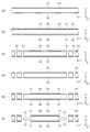
先ず、本発明にかかる素子としての振動素子について説明する。図1は、本発明に係る素子としての振動素子の実施形態における概略構成を示し、(a)は平面図、(b)は(a)に示すP−P断面図、(c)は(a)のQ−Q断面図である。図2は、水晶の結晶軸X、Y、ZをX軸の回りにθ回転してできた新直交座標軸X、Y’、Z’軸とATカット水晶基板との関係を示す模式図である。図3(a)〜(f)は、実施形態の振動素子の製造工程の概略を示す正断面図である。図4(g)〜(k)は、図3に示す製造工程に続く振動素子の製造工程の概略を示す正断面図である。
<Vibration element>
First, a vibration element as an element according to the present invention will be described. FIG. 1: shows schematic structure in embodiment of the vibration element as an element which concerns on this invention, (a) is a top view, (b) is PP sectional drawing shown to (a), (c) is (a It is QQ sectional drawing of). FIG. 2 is a schematic diagram showing the relationship between the new orthogonal coordinate axes X, Y ′, Z ′ and the AT-cut quartz substrate obtained by rotating the crystal axes X, Y, Z of the crystal by θ around the X axis. . 3A to 3F are front sectional views illustrating an outline of the manufacturing process of the resonator element according to the embodiment. 4G to 4K are front sectional views showing an outline of the vibration element manufacturing process subsequent to the manufacturing process shown in FIG. 3.
(振動素子の構成)
図1に示すように、本実施形態に係る圧電振動素子1は、中央に位置する多段メサ構造の励振部14、および励振部14の周縁に連設形成された薄肉の周辺部12を有する圧電基板10と、励振部14の両主面上に夫々対向配置された励振電極20a、20bと、各励振電極20a、20bから圧電基板10の端部に向かって延びる引出電極22a、22bと、引出電極22a、22bの端部であり且つ圧電基板10の2つの角隅部に夫々形成されたパッド24a、24bと、を備えている。
(Configuration of vibration element)
As shown in FIG. 1, the
圧電基板10は、その中央部に位置し主たる振動領域となる励振部14と、励振部14より薄肉で励振部14の全周縁に沿って鍔状に張出し形成された周辺部12と、を有している。平面形状がほぼ矩形である励振部14は、圧電基板10の略中央部を両主面方向へ多段(2段)に突出させた構成である。周辺部12は、励振部14の外周側面の厚み方向中間部から外径方向へ張出し形成されている。このように、圧電基板10は、側面が階段状をした励振部14と、励振部14の厚さの略中央部の周囲に連接された周辺部12と、を有している。なお、本例に係る周辺部12は、励振部14の全外周側面から鍔状に張出し形成されているが、外周側面の少なくとも一部の厚み方向中間部から外径方向へ張出し形成されている構成でもよい。
The
励振部14は、図1(a)に示すように、平面形状が、X軸方向を長辺とし、Z’軸方向を短辺とするほぼ矩形であり、中央部に一段メサ部15が設けられ、一段メサ部15の周囲に二段メサ部16が設けられている。二段メサ部16は、全ての側面17が段差状であって、その全周を周辺部12に囲まれており、周辺部12のY’軸方向の厚みよりも大きい厚み(厚肉)を有している。一段メサ部15は、全ての側面15aが段差状であって、その全周を二段メサ部16に囲まれており、二段メサ部16のY’軸方向の厚みよりも大きい厚み(厚肉)を有している。即ち、励振部14は、図1(b)および図1(c)に示すように、周辺部12に対してY’軸方向両方向に2段構造で突出している。図示の例では、励振部14は周辺部12に対して、+Y’軸側と−Y’軸側とに突出している。また、励振部14は、例えば対称の中心となる点(図示せず)を有し、この中心点に関して点対称(平面的、立体的に点対称)となる形状とすることができる。
As shown in FIG. 1A, the
このように励振部14は、厚みの異なる2種類の段差で構成され、その中央部に一段メサ部15が設けられ、一段メサ部15の周囲に二段メサ部16を有している。即ち、圧電振動素子1は、2段型の順メサ構造を有していると言える。励振部14は、厚みすべり振動を主振動として振動する。励振部14が2段型のメサ構造であることによって、圧電振動素子1は、エネルギー閉じ込め効果を有することができる。
As described above, the
励振電極20a、20bは、励振部14を構成する一段メサ部15の両主面上に夫々対向配置されている。表裏の励振電極20a、20bに交番電圧を印加すると、圧電振動素子1は、厚さに反比例した固有の振動周波数で励振される。励振された振動変位は周囲に広がり、振動変位が十分に減衰する領域の周辺部12の表裏面にパッド24a、24bが設けられている。
水晶等の圧電材料は三方晶系に属し、図2に示すように互いに直交する結晶軸X、Y、Zを有する。X軸、Y軸、Z軸は、夫々電気軸、機械軸、光学軸と呼称される。ATカット水晶基板101は、XZ面をX軸の回りに角度θだけ回転させた平面に沿って、水晶から切り出された平板である。ATカット水晶基板101の場合は、θは略35°15′である。なお、Y軸およびZ軸もX軸の周りにθ回転させて、夫々Y’軸、およびZ’軸とする。従って、ATカット水晶基板101は、直交する結晶軸X、Y’、Z’を有する。ATカット水晶基板101は、厚み方向がY’軸であって、Y’軸に直交するXZ’面(X軸およびZ’軸を含む面)が主面であり、厚みすべり振動が主振動として励振される。このATカット水晶基板101を加工して、圧電基板10を得ることができる。
A piezoelectric material such as quartz belongs to the trigonal system and has crystal axes X, Y, and Z orthogonal to each other as shown in FIG. The X axis, the Y axis, and the Z axis are referred to as an electric axis, a mechanical axis, and an optical axis, respectively. The AT-cut
即ち、圧電基板10は、図2に示すようにX軸(電気軸)、Y軸(機械軸)、Z軸(光学軸)からなる直交座標系のX軸を中心として、Z軸をY軸の−Y方向へ傾けた軸をZ’軸とし、Y軸をZ軸の+Z方向へ傾けた軸をY’軸とし、X軸とZ’軸に平行な面で構成され、Y’軸に平行な方向を厚みとするATカット水晶基板101からなる。
That is, as shown in FIG. 2, the
圧電基板10は、図1(a)に示すように、Y’軸に平行な方向(以下、「Y’軸方向」という)を厚み方向として、X軸に平行な方向(以下、「X軸方向」という)を長辺とし、Z’軸に平行な方向(以下、「Z’軸方向」という)を短辺とする矩形の形状を有することができる。圧電基板10は、励振部14と、励振部14の周縁に沿って形成された周辺部12と、を有する。ここで、「矩形の形状」とは、文字通りの矩形状と、各角部が面取りされた略矩形をも含むものとする。
As shown in FIG. 1A, the
(振動素子の製造方法)
次に、図3、および図4を参照して振動素子の製造方法について説明する。図3、および図4は、本発明に係る振動素子の製造工程(製造方法)の概略を模式的に示す正断面図である。なお、図4および図5は、図1(b)に対応しており、Z’軸方向から見た断面を示している。
(Manufacturing method of vibration element)
Next, a method for manufacturing a vibration element will be described with reference to FIGS. 3 and 4 are front sectional views schematically showing the outline of the manufacturing process (manufacturing method) of the resonator element according to the invention. 4 and 5 correspond to FIG. 1B and show a cross section viewed from the Z′-axis direction.
先ず、図3(a)に示すように、ATカット水晶基板101の表裏主面(XZ’平面に平行な面)に耐蝕膜30を形成する。耐蝕膜30は、例えば、スパッタ法や真空蒸着法などによりクロム(Cr)および金(Au)をこの順で積層した後、このクロムおよび金を所望の形状にパターニングすることによって形成される。このパターニングは、例えば、次段落で説明するフォトリソグラフィ技術およびエッチング技術によって行われる。耐蝕膜30は、ATカット水晶基板101を加工する際に、エッチング液となるフッ酸(HF)を含む溶液に対して耐蝕性を有する。
First, as shown in FIG. 3A, the corrosion-
次に、図3(b)に示すように、耐蝕膜30上にフォトレジスト膜を塗布した後、このフォトレジスト膜を露光および現像して、所定の形状にフォトレジスト膜が除去された開口部41、42を有するレジスト膜40を形成する。このようにして、レジスト膜40は、耐蝕膜30の一部を覆うように形成される。
Next, as shown in FIG. 3B, after applying a photoresist film on the corrosion-
次に、図3(c)に示すように、レジスト膜40をマスクとして耐蝕膜30、およびATカット水晶基板101の外形部分31、32をエッチングする。耐蝕膜30のエッチングは、マスクの開口部41、42に露出した金を、例えば、ヨウ化カリウム溶液を用いてエッチング(除去)し、次いで金が除去されて露出したクロムを、例えば、硝酸2セリウムアンモニウム溶液によりエッチング(除去)する。ATカット水晶基板101の外形部分31、32のエッチングは、耐蝕膜30がエッチングされて露出したATカット水晶基板101を、例えば、フッ化アンモニウム(NH4F)とフッ化水素酸(フッ酸;HF)と水(H2O)の混合水溶液(バッファードフッ酸)をエッチング液として行われる。
Next, as shown in FIG. 3C, the corrosion
なお、本例では、混合比が、フッ化アンモニウム(NH4F):フッ化水素酸(フッ酸;HF):水(H2O)=30.8wt%:14.2wt%:55.0wt%の混合水溶液(バッファードフッ酸)を用いた。即ち、本例でのフッ化アンモニウム(NH4F)とフッ化水素酸(フッ酸;HF)との混合比は、フッ化アンモニウム(NH4F):フッ化水素酸(フッ酸;HF)=2.2wt%:1wt%となっている。このように本例では、フッ化アンモニウム(NH4F)とフッ化水素酸(フッ酸;HF)との混合比が、2.2wt%:1wt%の混合液を用いたが、フッ化アンモニウム(NH4F)とフッ化水素酸(フッ酸;HF)との混合比は、フッ化アンモニウム(NH4F):フッ化水素酸(フッ酸;HF)=1.5wt%以上2.5wt%以下:1wt%の範囲であれば適用可能である。また、本工程での混合水溶液(バッファードフッ酸)の温度(液温)は、85℃に設定してエッチングを行った。 In this example, the mixing ratio is ammonium fluoride (NH 4 F): hydrofluoric acid (hydrofluoric acid; HF): water (H 2 O) = 30.8 wt%: 14.2 wt%: 55.0 wt % Mixed aqueous solution (buffered hydrofluoric acid) was used. That is, the mixing ratio of ammonium fluoride (NH 4 F) and hydrofluoric acid (hydrofluoric acid; HF) in this example is ammonium fluoride (NH 4 F): hydrofluoric acid (hydrofluoric acid; HF). = 2.2 wt%: 1 wt%. As described above, in this example, a mixed solution having a mixing ratio of ammonium fluoride (NH 4 F) and hydrofluoric acid (hydrofluoric acid; HF) of 2.2 wt%: 1 wt% was used. The mixing ratio of (NH 4 F) and hydrofluoric acid (hydrofluoric acid; HF) is ammonium fluoride (NH 4 F): hydrofluoric acid (hydrofluoric acid; HF) = 1.5 wt% or more and 2.5 wt% % Or less: 1 wt% is applicable. In addition, the temperature (liquid temperature) of the mixed aqueous solution (buffered hydrofluoric acid) in this step was set to 85 ° C. for etching.
続いて、レジスト膜40をアッシング(レジスト剥離)することによって、図3(d)に示すように、表裏主面に耐蝕膜30が設けられた圧電基板10の外形(Y’軸方向から見たときの形状)が形成される。
Subsequently, by ashing (resist stripping) the resist
次に、図3(e)に示すように、耐蝕膜30上にフォトレジスト膜を塗布した後、このフォトレジスト膜を露光および現像して、所定の形状にフォトレジスト膜が除去された開口部51を有するレジスト膜50を形成する。このようにして、レジスト膜50は、耐蝕膜30の一部を覆うように形成される。
Next, as shown in FIG. 3E, after applying a photoresist film on the corrosion-
次に、図3(e)に示すレジスト膜50をマスクとして、レジスト膜50の開口部51に露出する耐蝕膜30、およびATカット水晶基板101をエッチングし、周辺部12を形成する。耐蝕膜30のエッチングは、前述のATカット水晶基板101の外形形成と同様に、マスクとしてのレジスト膜50の開口部51に露出した金を、例えば、ヨウ化カリウム溶液を用いてエッチング(除去)し、次いで金が除去されて露出したクロムを、例えば、硝酸2セリウムアンモニウム溶液によりエッチング(除去)する。ATカット水晶基板101のエッチングは、耐蝕膜30がエッチングされて露出したATカット水晶基板101を、例えば、フッ化水素酸(フッ酸:HF)とフッ化アンモニウム(NH4F)と水(H2O)との混合水溶液をエッチング液として行われる。ここで用いる混合水溶液(バッファードフッ酸)は、前述の圧電基板10の外形を形成する際に用いたものと同じ組成の混合水溶液(バッファードフッ酸)であり、且つ同じ温度(液温)でエッチング加工を行う。
Next, using the resist
図3(f)に示すように、ATカット水晶基板101のエッチングは、所定の深さまでハーフエッチングされ、薄肉の周辺部12が形成される。その後、レジスト膜50の剥離、および耐蝕膜30のアッシング(耐蝕膜剥離)を行うことによって、図4(g)に示すように、周囲に周辺部12が設けられ、周辺部12の表裏面と交差する面である側面17から延在する厚肉部(凸部)を有する圧電基板10が形成される。ここで外枠35も形成され、部分的に圧電基板10と外枠35とが連結されているが、図示は省略している。
As shown in FIG. 3F, the AT cut
次に、二段メサ部16を形成する工程について説明する。先ず、前述した図4(g)に示す圧電基板10を含むATカット水晶基板101の露出面に、図4(h)に示すような耐蝕膜60を形成する。耐蝕膜60は、例えば、スパッタ法や真空蒸着法などによりクロム(Cr)および金(Au)をこの順で積層した後、このクロムおよび金を所望の形状にパターニングすることによって形成される。このパターニングは、例えば、次段落で説明するフォトリソグラフィ技術およびエッチング技術によって行われる。耐蝕膜60は、ATカット水晶基板101を加工する際に、エッチング液となるフッ酸を含む溶液に対して耐蝕性を有する。
Next, a process for forming the two-
次に、図4(i)に示すように、耐蝕膜60上にフォトレジスト膜を塗布した後、このフォトレジスト膜を露光および現像して、所定の形状にフォトレジスト膜が除去された開口部71を有するレジスト膜70を形成する。このようにして、レジスト膜70は、耐蝕膜60の一部を覆うように形成される。
Next, as shown in FIG. 4 (i), after applying a photoresist film on the corrosion-
次に、図4(j)に示すように、レジスト膜70をマスクとして耐蝕膜60、および圧電基板10の二段メサ部16をエッチングする。耐蝕膜60のエッチングは、マスクの開口部71に露出した金を、例えば、ヨウ化カリウム溶液を用いてエッチング(除去)し、次いで金が除去されて露出したクロムを、例えば、硝酸2セリウムアンモニウム溶液によりエッチング(除去)する。圧電基板10のエッチングは、耐蝕膜60がエッチングされて露出した圧電基板10を含むATカット水晶基板101を、例えば、フッ化水素酸(フッ酸:HF)とフッ化アンモニウム(NH4F)と水(H2O)の混合水溶液(バッファードフッ酸)をエッチング液として行われる。
Next, as shown in FIG. 4J, the corrosion
なお、本例では前述した外形形状の形成と同様に、混合比が、フッ化アンモニウム(NH4F):フッ化水素酸(フッ酸;HF):水(H2O)=30.8wt%:14.2wt%:55.0wt%の混合水溶液(バッファードフッ酸)を用いた。また、本例でのフッ化アンモニウム(NH4F)とフッ化水素酸(フッ酸;HF)との混合比は、フッ化アンモニウム(NH4F):フッ化水素酸(フッ酸;HF):=2.2wt%:1wt%となっている。このように本例では、フッ化アンモニウム(NH4F)とフッ化水素酸(フッ酸;HF)との混合比が、2.2wt%:1wt%の混合液を用いたが、フッ化アンモニウム(NH4F)とフッ化水素酸(フッ酸;HF)との混合比は、フッ化水素酸(フッ酸;HF)に対するフッ化アンモニウム(NH4F)の重量比が1.5以上2.5以下の範囲であれば適用可能である。また、本工程での混合水溶液(バッファードフッ酸)の温度(液温)は、35℃に設定してエッチングを行った。なお、フッ化アンモニウム(NH4F)は、NH4HF2であってもよい。 In this example, similarly to the formation of the outer shape described above, the mixing ratio is ammonium fluoride (NH 4 F): hydrofluoric acid (hydrofluoric acid; HF): water (H 2 O) = 30.8 wt%. : 14.2 wt%: 55.0 wt% mixed aqueous solution (buffered hydrofluoric acid) was used. The mixing ratio of ammonium fluoride (NH 4 F) and hydrofluoric acid (hydrofluoric acid; HF) in this example is ammonium fluoride (NH 4 F): hydrofluoric acid (hydrofluoric acid; HF). : = 2.2 wt%: 1 wt% As described above, in this example, a mixed solution having a mixing ratio of ammonium fluoride (NH 4 F) and hydrofluoric acid (hydrofluoric acid; HF) of 2.2 wt%: 1 wt% was used. (NH 4 F) and hydrofluoric acid; mixing ratio of the (hydrofluoric acid HF) is hydrofluoric acid wherein the weight ratio of (hydrofluoric acid HF) ammonium fluoride for (NH 4 F) of 1.5 or more 2 It can be applied within the range of .5 or less. In addition, the temperature (liquid temperature) of the mixed aqueous solution (buffered hydrofluoric acid) in this step was set to 35 ° C. for etching. The ammonium fluoride (NH 4 F) may be NH 4 HF 2 .
ATカット水晶基板101のエッチングは、圧電基板10の厚肉部の外周部分を除くATカット水晶基板101に行われ、二段メサ部16の所定の深さである側面17の中間部までハーフエッチングすることによって、二段メサ部16が形成される。この工程でのATカット水晶基板101のエッチングは、耐蝕膜60の形成されている圧電基板10の中央部を除くATカット水晶基板101に対して行われるため、既にエッチングされた部分である周辺部12や側面17(二段メサ部16の段部(凸部))に対してもエッチングが行われてしまう。換言すれば、さらにエッチングが進んでしまう追加エッチングが行われてしまう。
The AT-
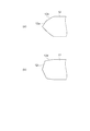
この追加エッチングの影響と本実施形態のエッチング方法の効果について、図5、および図6を用いて説明する。図5は、水晶板の露出面のエッチング状態を説明するための図1に示すR部の拡大図であり、(a)、(b)は従来の方法によるエッチング状態を示し、(c)、(d)は本実施形態の方法によるエッチング状態を示す正断面図である。また、図6は、水晶板の抜き加工面である振動素子外周の露出面(水晶外形)のエッチング状態を説明するための拡大図であり、(a)は従来の方法によるエッチング状態を示し、(b)は本発明に係る実施形態によるエッチング状態を示す正断面図である。 The influence of this additional etching and the effect of the etching method of this embodiment will be described with reference to FIGS. FIGS. 5A and 5B are enlarged views of the R portion shown in FIG. 1 for explaining the etching state of the exposed surface of the crystal plate. FIGS. 5A and 5B show the etching state by the conventional method, and FIGS. (D) is a front sectional view showing an etching state by the method of the present embodiment. FIG. 6 is an enlarged view for explaining an etching state of an exposed surface (crystal outer shape) on the outer periphery of the vibration element that is a punched surface of the crystal plate, and (a) shows an etching state by a conventional method, (B) is a front sectional view showing an etching state according to an embodiment of the present invention.
先ず、図5(a)、(b)を用いて、従来のエッチング方法の二段メサ部の形成における水晶板のエッチング状態について説明する。二段メサ部16の形成は、既に外形加工がなされ、交差して露出する水晶板の2面である周辺部12と、側面15aと、耐蝕膜60に覆われていない水晶面(二段メサ部16となる部分)とが、フッ化水素(HF)を含むエッチング液によってエッチングされることによって行われる。
First, the etching state of the crystal plate in the formation of the two-step mesa portion of the conventional etching method will be described with reference to FIGS. The formation of the two-
従来の水晶板のエッチング方法におけるエッチング液としては、前述で説明した本発明に係る振動素子の製造方法で説明したフッ化水素酸(フッ酸:HF)を含む混合水溶液(バッファードフッ酸)を用いている。詳述すると、混合比が、フッ化アンモニウム(NH4F):フッ化水素酸(フッ酸;HF):水(H2O)=30.8wt%:14.2wt%:55.0wt%の混合水溶液(バッファードフッ酸)を用いる。そして、エッチング液の温度(液温)を65℃に設定して行われていた。これは、エッチング液の温度を高くすることによってエッチング速度を早くし、エッチングの工数を少なくするためである。 As an etchant in a conventional quartz plate etching method, a mixed aqueous solution (buffered hydrofluoric acid) containing hydrofluoric acid (hydrofluoric acid: HF) described in the method for manufacturing a vibration element according to the present invention described above is used. Used. Specifically, the mixing ratio is ammonium fluoride (NH 4 F): hydrofluoric acid (hydrofluoric acid; HF): water (H 2 O) = 30.8 wt%: 14.2 wt%: 55.0 wt% A mixed aqueous solution (buffered hydrofluoric acid) is used. And it was performed by setting the temperature (liquid temperature) of etching liquid to 65 degreeC. This is because the etching rate is increased by increasing the temperature of the etching solution, and the number of etching steps is reduced.
このように高温のエッチング液で二段メサ部16をエッチング加工すると、図5(a)に示す矢印のように、既に外形加工がなされ、交差して露出する水晶板の2面である周辺部12と側面17とが、再度フッ化水素(HF)を含むエッチング液に晒され、追加エッチングされる。特に、側面17の図示X軸方向のエッチングが大きくなるため、二段メサ部16のエッチングに加えて側面17のエッチングが重なり、図5(b)に示すように、二段メサ部16と側面17とが交差する部分18が大きく削られる(侵食される)と共に形状のばらつきが大きくなってしまう。
When the two-
このように、二段メサ部16の外周の側面17の形状が大きく変形したり、形状がばらついたりすることによって、振動エネルギー閉じ込め効果がばらつき、振動素子の電気的特性、特に、発振のし易さの目安となるCI(Crystal Impedance)値の劣化、ばらつきを生じてしまっていた。
As described above, when the shape of the outer
このような従来のエッチング方法に対し、本発明に係るエッチング方法によれば、二段メサ部16の外周の側面17の形状を安定させることができる。このことについて、図5(c)、(d)を用いて説明する。本発明に係るエッチング方法では、エッチング液は従来の物と同様であるが、エッチング液の温度(液温)が異なる。従来のエッチング液の温度が65℃であったのに対し、本発明に係るエッチング方法でのエッチング液の温度は、35℃に設定されている。
In contrast to such a conventional etching method, according to the etching method of the present invention, the shape of the
このように、35℃と低い温度にエッチング液の温度を設定し、二段メサ部16をエッチング加工することにより、エッチング速度が遅くなる。特に図5(c)に示すように、X軸方向のエッチングの進みが遅くなる。これにより、図5(d)に示すように、二段メサ部16と側面17とが交差する部分19の侵食を小さくすることができる。このように侵食を小さくすることによって形状のばらつきも小さくすることができる。
Thus, the etching rate is lowered by setting the temperature of the etching solution to a low temperature of 35 ° C. and etching the two-
このように、二段メサ部16の外周の側面17の形状の変形を小さくでき、さらに形状のばらつきが小さくできることによって、振動エネルギー閉じ込め効果を安定的に行うことができるため、振動素子の電気的特性、特に、CI値の劣化を防止し安定した発振を行うことが可能な振動素子を提供することが可能となった。
As described above, since the deformation of the shape of the
また、本発明に係るエッチング方法によれば、エッチングによる二段メサ部の形成における圧電基板10の外形形状のばらつきも小さくすることが可能となる。このことについて、図6を用いて説明する。なお、前述と同様な説明は省略し、異なる項目について説明する。図6は、水晶板の抜き加工面である振動素子外周の露出面(外形端面)のエッチング状態を説明するための拡大図であり、(a)は従来の方法によるエッチング状態を示し、(b)は本発明に係る実施形態によるエッチング状態を示す正断面図である。
Further, according to the etching method of the present invention, it is possible to reduce variations in the outer shape of the
図6(a)に示す、従来のエッチング液の温度を85℃にするエッチング方法では、水晶板の抜き加工面である振動素子外周の露出面12a、12b(水晶板の外形端面)と、露出面12bと交差する周辺部12の露出面との2面が、図示しない二段メサ部を形成するためのエッチング液に晒される。エッチング液に晒された露出面12aおよび露出面12aと周辺部12の露出面との交差部分である露出面12bは、前述と同様に早いエッチング速度でエッチングが進み、傾斜面が大きくなると共に形状のばらつきも大きくなる。
In the etching method in which the temperature of the conventional etching solution shown in FIG. 6A is 85 ° C., the exposed
それに対し、図6(b)に示す、本発明に係る実施形態のエッチング液の温度を35℃に設定したエッチング方法では、水晶板の抜き加工面である振動素子外周の露出面12c、12d(水晶板の外形端面)と、露出面12dと交差する周辺部12の露出面との2面が、図示しない二段メサ部を形成するためのエッチング液に晒される。なお、ここで露出面12cと露出面12dとによって凸部が形成されている。エッチング液に晒された露出面12cおよび露出面12cと周辺部12の露出面との交差部分である露出面12dは、前述と同様にエッチングが進むが進行速度が遅くなり、結果として傾斜面が小さくなると共に形状のばらつきも小さくすることができる。
On the other hand, in the etching method in which the temperature of the etching solution according to the embodiment of the present invention shown in FIG. The two surfaces of the quartz plate and the exposed surface of the
次に、図4に戻り、二段メサ部16をエッチング加工する工程に続く工程について説明する。図4(k)に示すように、二段メサ部16がエッチング加工された圧電基板10を含むATカット水晶基板101から、レジスト膜70をアッシング(レジスト剥離)する。これによって、一段メサ部15の表裏の主面に励振電極20a、20bが設けられた圧電基板10が形成される。なお、励振電極20a、20bは、耐蝕膜60をそのまま用いて形成される。
Next, returning to FIG. 4, a process following the process of etching the two-
以上の工程によって、厚みの異なる2種類の段差、即ち中央部に一段メサ部15が設けられ、一段メサ部15の周囲に二段メサ部16を有し、その周囲に周辺部12を有している圧電振動素子1が設けられたATカット水晶基板101が形成される。
Through the above steps, two types of steps having different thicknesses, that is, a one-
(製造方法の変形例)
なお、前述した振動素子の製造方法に変えて下記の変形例における工程でも圧電振動素子1が設けられたATカット水晶基板101実現可能である。なお、前述の実施形態と同様な構成には、図4および図5と同符号を付し、同図を適宜参照ながら説明する。
(Modification of manufacturing method)
Note that the AT-
耐蝕膜30上にポジ型のフォトレジスト膜を塗布した後、このフォトレジスト膜を露光および現像して、所定の形状(開口部41、42など)を有するレジスト膜40を形成する。そして、このレジスト膜40の開口部41、42の部分の耐蝕膜30、およびATカット水晶基板101をエッチングして圧電振動素子1外形を形成する。
After a positive photoresist film is applied on the corrosion-
次に、マスクを用いて再度レジスト膜40の一部(周辺部12に対応する部分)を露光および現像して、所定の形状(開口部51)を有するレジスト膜50を形成する。即ち、マスクをY’軸方向から見てレジスト膜40の外縁の内側に配置して露光を行う。そして、このレジスト膜50の開口部51の部分の耐蝕膜30、およびATカット水晶基板101をエッチングして圧電振動素子1の周辺部12を形成する。
Next, a part of resist film 40 (a part corresponding to peripheral part 12) is exposed and developed again using a mask to form resist
次に、マスクを用いて再度レジスト膜50の一部(二段メサ部16に対応する部分)を露光および現像して、所定の形状(開口部71)を有するレジスト膜70を形成する。即ち、マスクをY’軸方向から見てレジスト膜50の外縁の内側に配置して露光を行う。そして、このレジスト膜70の開口部71の部分の耐蝕膜30、およびATカット水晶基板101をエッチングして圧電振動素子1の二段メサ部16を形成する。以上のような変形例としての製造方法を用いても、二段メサ部16を有する圧電振動素子1を製造することができる。
Next, a part of the resist film 50 (a part corresponding to the two-step mesa part 16) is again exposed and developed using a mask to form a resist
上述の振動素子の製造方法を用いた振動素子によれば、二段メサ部16の形成時に生じる二段メサ部16と側面17とが交差する部分19の侵食を小さくすることができる。また、この侵食を小さくすることによって形状のばらつきも小さくすることができる。図7に沿って、本実施形態の製造方法における効果について説明する。図7には、圧電振動素子1の外形寸法の分布および振動特性(CI値)の分布を示してある。図7(a)が従来方法で形成した圧電振動素子1(24MHz)の外形寸法であり、(b)が本実施形態で形成した圧電振動素子1(24MHz)の外形寸法の実測値分布であり、(c)が従来方法で形成した圧電振動素子1(24MHz)のCI値分布であり、(d)が本実施形態で形成した圧電振動素子1(24MHz)のCI値分布である。なお、図7(a)、(b)は、縦軸に外形寸法の設計値をゼロとしたときの測定品ごとの寸法差、横軸に発生数(度数)を示した、所謂寸法ばらつき分布(偏差)を表している。
According to the vibration element using the above-described method for manufacturing a vibration element, it is possible to reduce erosion of the
図7(a)、(b)に示すように、本実施形態の製造方法を用いた圧電振動素子1の外形寸法のばらつきは、従来方法の外形寸法のばらつきの1/2以内に収まっていることが分かる。また、図7(c)、(d)に示すように、圧電振動素子1(24MHz)のCI値分布においても、本実施形態の製造方法を用いた圧電振動素子1は、一般的な規格値である95Ω以下に殆んど収まっている(良品率95%以上)。これに対し、従来方法の製造方法を用いた圧電振動素子1は、約1/3が規格値以上、即ち不良となってしまっていることが分かる。
As shown in FIGS. 7A and 7B, the variation in the outer dimensions of the
このように、二段メサ部16の外周の側面17の形状の変形を小さくでき、さらに形状のばらつきが小さくできることによって、振動エネルギー閉じ込め効果を安定的に行うことができるため、振動素子の電気的特性、特に、CI値の劣化を防止し安定した発振を行うことが可能な振動素子を提供することが可能である。また、CI値の良品率を高めることができるため、不良コストの削減につながり、結果としてコスト低減を実現することが可能となる。
As described above, since the deformation of the shape of the
なお、エッチング液(バッファードフッ酸)のエッチング時の温度(液温)は、前述の実施形態では35℃の例で説明したがこの温度に限らない。図8は、バッファードフッ酸の温度と圧電振動素子1の不良率との相関を示している。図8に示すように、バッファードフッ酸の温度を25℃以上55℃以下(図示の範囲1)とすることで、許容できる不良率であるとされるPn=10%以下を達成することができる。なお、25℃未満では混合液の析出、液温の管理などが困難となり実用性に適しない。このように、バッファードフッ酸の温度は、25℃以上55℃以下とすることが好ましい。
In addition, although the temperature (liquid temperature) at the time of etching of etching liquid (buffered hydrofluoric acid) demonstrated by the example of 35 degreeC in the above-mentioned embodiment, it is not restricted to this temperature. FIG. 8 shows the correlation between the temperature of the buffered hydrofluoric acid and the defect rate of the
また、エッチング液(バッファードフッ酸)のエッチング時の温度(液温)は、30℃以上38℃以下(図示の範囲2)とすることがさらに好適である。これは、バッファードフッ酸の温度管理のし易さ(加工精度の向上)、エッチングスピードの好適さ(加工工数の低減)、あるいは図8に示すように不良率が少ない(Pn=5%以下)ことによる製造コスト低減など、さらに好適な温度範囲となる。
Further, the temperature (liquid temperature) at the time of etching with the etching solution (buffered hydrofluoric acid) is more preferably 30 ° C. or more and 38 ° C. or less (
前述の説明では、振動素子としてATカット水晶基板101を用いた圧電振動素子1を例に説明したが、振動素子としては本例に限らない。本発明は、露出して交差する2つの面が、エッチング液にさらされる水晶板を用いた構成であればよく、例えば、音叉型水晶振動片など他のカット角で切り出された水晶基板を用いた振動片にも提供可能である。また、振動片に限らず、例えば、圧力センサー素子、ジャイロセンサー素子などにも適用することができる。
In the above description, the
また、前述の説明では、振動素子としてATカット水晶基板101を用いた、多段(2段)順メサ構造の圧電振動素子1を例に説明したがこれに限らず、1段順メサ構造、3段以上の多段順メサ構造、或いは逆メサ構造などの構成の圧電振動片にも適用することができる。
In the above description, the multi-stage (two-stage) forward mesa structure
また、前述の説明では、圧電基板10の外形形成、および周辺部12の形成においては、エッチング液の温度を85℃としてエッチングする例で説明したがこれに限らず、二段メサ部16の形成時と同様なエッチング液およびエッチング液の温度(液温)を用いることもできる。
In the above description, the example of forming the outer shape of the
<電子デバイス>
次に、上記実施形態で述べた振動素子を備えた電子デバイスについて説明する。先ず、振動子について図9を参照しながら説明し、次に発振器について図10を参照しながら説明する。
<Electronic device>
Next, an electronic device including the vibration element described in the above embodiment will be described. First, the vibrator will be described with reference to FIG. 9, and then the oscillator will be described with reference to FIG.
(振動子)
電子デバイスとしての振動子について図9を用いて説明する。図9は、本発明にかかる振動素子を用いた電子デバイスとしての振動子を示す正断面図である。図9に示すように、振動子200は、上記実施形態で説明したATカット水晶基板101を用いた圧電振動素子1と、圧電振動素子1を収容したパッケージ204と、パッケージ204を気密に封止する蓋体としてのリッド208とを備えている。
(Vibrator)
A vibrator as an electronic device will be described with reference to FIG. FIG. 9 is a front sectional view showing a vibrator as an electronic device using the vibration element according to the present invention. As shown in FIG. 9, the
パッケージ204は、平板上の第1基板201と、第1基板201上に、枠状の第2基板202、枠状の第3基板203、を順に積層、固着して形成され、圧電振動素子1が収容される凹部が形成される。第1基板201、第2基板202、第3基板203は、例えばセラミックスなどにより形成される。
The package 204 is formed by sequentially laminating and fixing a
第2基板202は、圧電振動素子1の励振部が含まれる大きさの開口を有する枠状の形状に形成されている。第3基板203は、第2基板202の開口より広い開口を有する枠状の形状に形成され、第2基板202上に積層され、固着される。そして第2基板202に第3基板203が積層されて第3基板203の開口の内側に現れる第2基板202の露出面に、圧電振動素子1が接続固着されている。第2基板202の露出面には、図示しない電極が設けられており、その電極に圧電振動素子1が導電性接着剤206によって接続固着される。なお、図示しない電極は、図示しないパッケージ204の内部配線により第1基板201の外部底面に設けられた複数の外部接続端子209に電気的に接続されている。
The second substrate 202 is formed in a frame shape having an opening having a size including the excitation portion of the
更に、第3基板203の開口の上側に蓋体としてのリッド208が配置され、パッケージ204の開口を封止し、パッケージ204の内部が気密封止され、振動子200が得られる。リッド208は、例えば、42アロイ(鉄にニッケルが42%含有された合金)やコバール(鉄、ニッケルおよびコバルトの合金)等の金属、セラミックス、あるいはガラスなどを用いて形成することができる。例えば、金属によりリッド208を形成した場合には、コバール合金などを矩形環状に型抜きして形成されたシールリング207を介してシーム溶接することによりパッケージ204と接合される。パッケージ204およびリッド208によって形成される凹部空間205は、圧電振動素子1が動作するための空間となるため、減圧空間(真空に近い空間)または窒素、ヘリウム、アルゴンなどの不活性ガス雰囲気に密閉・封止することが好ましい。
Further, a
上述した振動子200によれば、前述した圧電振動素子1を備えていることから、振動エネルギー閉じ込め効果を安定的に行うことができ、電気的特性、特に、CI値の劣化がされた安定した発振を行うことが可能な振動子を提供することができる。
According to the
(発振器)
電子デバイスとしての発振器について図10を用いて説明する。図10は、本発明にかかる振動素子を用いた電子デバイスとしての発振器を示す正断面図である。図10に示すように、発振器300は、上記実施形態で説明したATカット水晶基板101を用いた圧電振動素子1と、圧電振動素子1を収容したパッケージ304と、パッケージ304を気密に封止する蓋体としてのリッド308とを備えている。
(Oscillator)
An oscillator as an electronic device will be described with reference to FIG. FIG. 10 is a front sectional view showing an oscillator as an electronic device using the resonator element according to the invention. As shown in FIG. 10, the
パッケージ304は、平板上の第1基板301と、第1基板301上に、枠状の第2基板302、第3基板303を順に積層、固着して形成され、半導体装置310と圧電振動素子1とが収容される凹部が形成される。第1基板301、第2基板302、および第3基板303は、例えばセラミックスなどにより形成される。
The
第1基板301は、凹部側の半導体装置310が搭載される電子部品搭載面に、半導体装置310が載置され固定されるダイパッド(図示せず)が設けられている。半導体装置310はダイパッド上に、例えば、図示しない導電性接着剤(ダイアタッチ材)によって接着され、固定されている。さらに、第1基板301の電子部品搭載面には、半導体装置310の図示しない電極パッドと電気的に接続するボンディングワイヤー311が接続される複数のIC接続端子(図示せず)が形成されている。そして、半導体装置310の電極パッドとIC接続端子とが、ワイヤーボンディング法を用いて電気的に接続されている。また、IC接続端子のいずれかは、パッケージ304の図示しない内部配線により、第1基板301の外部底面に設けられた複数の外部接続端子309に電気的に接続されている。
The
半導体装置310は、圧電振動素子1を駆動振動させるための励振手段としての駆動回路などを有している。具体的には、半導体装置310が有する駆動回路は、圧電振動素子1を駆動させ、受信した駆動信号を増幅するなどして外部に供給する。
The
第2基板302は、搭載される半導体装置310が収容可能な大きさの開口を有する枠状の形状に形成されている。第3基板303は、第2基板302の開口より広い開口を有する枠状の形状に形成され、第2基板302上に積層され、固着される。そして第2基板302に第3基板303が積層されて第3基板303の開口の内側に現れる第2基板302の露出面に、圧電振動素子1が接続固着されている。第2基板302の露出面には、図示しない電極が設けられており、その電極に圧電振動素子1が導電性接着剤306によって接続固着される。なお、図示しない電極は、図示しないパッケージ204の内部配線により図示しないIC接続端子に電気的に接続されている。
The
更に、第3基板303の開口の上側に蓋体としてのリッド308が配置され、パッケージ304の開口を封止し、パッケージ304の内部が気密封止され、発振器300が得られる。リッド308は、例えば、42アロイ(鉄にニッケルが42%含有された合金)やコバール(鉄、ニッケルおよびコバルトの合金)等の金属、セラミックス、あるいはガラスなどを用いて形成することができる。例えば、金属によりリッド308を形成した場合には、コバール合金などを矩形環状に型抜きして形成されたシールリング307を介してシーム溶接することによりパッケージ304と接合される。パッケージ304およびリッド308によって形成される凹部空間305は、圧電振動素子1が動作するための空間となるため、減圧空間(真空に近い空間)または窒素、ヘリウム、アルゴンなどの不活性ガス雰囲気に密閉・封止することが好ましい。
Further, a
上述した発振器300によれば、前述した圧電振動素子1を備えていることから、振動エネルギー閉じ込め効果を安定的に行うことができ、電気的特性、特に、CI値の劣化がされた安定した発振を行うことが可能な発振器を提供することができる。
According to the
<電子機器>
次いで、本発明の一実施形態に係る振動素子としての圧電振動素子1、圧電振動素子1を用いた振動子200、あるいは圧電振動素子1を用いた発振器300を適用した電子機器について、図11〜図13に基づき、詳細に説明する。なお、説明では、圧電振動素子1を用いた振動子200を適用した例を示している。
<Electronic equipment>
Next, regarding an electronic device to which the
図11は、本発明の一実施形態に係る振動子200を備える電子機器としてのモバイル型(又はノート型)のパーソナルコンピューターの構成の概略を示す斜視図である。この図において、パーソナルコンピューター1100は、キーボード1102を備えた本体部1104と、表示部100を備えた表示ユニット1106とにより構成され、表示ユニット1106は、本体部1104に対しヒンジ構造部を介して回動可能に支持されている。このようなパーソナルコンピューター1100には、基準信号源などとして振動子200が内蔵されている。
FIG. 11 is a perspective view schematically illustrating a configuration of a mobile (or notebook) personal computer as an electronic apparatus including the
図12は、本発明の一実施形態に係る振動子200を備える電子機器としての携帯電話機(PHSも含む)の構成の概略を示す斜視図である。この図において、携帯電話機1200は、複数の操作ボタン1202、受話口1204および送話口1206を備え、操作ボタン1202と受話口1204との間には、表示部100が配置されている。このような携帯電話機1200には、基準信号源などとして振動子200が内蔵されている。
FIG. 12 is a perspective view schematically illustrating a configuration of a mobile phone (including PHS) as an electronic device including the
図13は、本発明の一実施形態に係る振動子200を備える電子機器としてのデジタルスチールカメラの構成の概略を示す斜視図である。なお、この図には、外部機器との接続についても簡易的に示されている。ここで、通常のカメラは、被写体の光像により銀塩写真フィルムを感光するのに対し、デジタルスチールカメラ1300は、被写体の光像をCCD(Charge Coupled Device)等の撮像素子により光電変換して撮像信号(画像信号)を生成する。デジタルスチールカメラ1300におけるケース(ボディー)1302の背面には、表示部100が設けられ、CCDによる撮像信号に基づいて表示を行う構成になっており、表示部100は、被写体を電子画像として表示するファインダーとして機能する。また、ケース1302の正面側(図中裏面側)には、光学レンズ(撮像光学系)やCCD等を含む受光ユニット1304が設けられている。
FIG. 13 is a perspective view illustrating a schematic configuration of a digital still camera as an electronic apparatus including the
撮影者が表示部100に表示された被写体像を確認し、シャッターボタン1306を押下すると、その時点におけるCCDの撮像信号が、メモリー1308に転送・格納される。また、このデジタルスチールカメラ1300においては、ケース1302の側面に、ビデオ信号出力端子1312と、データ通信用の入出力端子1314とが設けられている。そして、図示されるように、ビデオ信号出力端子1312にはテレビモニター1430が、データ通信用の入出力端子1314にはパーソナルコンピューター1440が、それぞれ必要に応じて接続される。さらに、所定の操作により、メモリー1308に格納された撮像信号が、テレビモニター1430や、パーソナルコンピューター1440に出力される構成になっている。このようなデジタルスチールカメラ1300には、基準信号源などとして振動子200が内蔵されている。
When the photographer confirms the subject image displayed on the
なお、本発明の一実施形態に係る振動子200は、図11のパーソナルコンピューター(モバイル型パーソナルコンピューター)、図12の携帯電話機、図13のデジタルスチールカメラの他にも、例えば、インクジェット式吐出装置(例えばインクジェットプリンター)、ラップトップ型パーソナルコンピューター、テレビ、ビデオカメラ、ビデオテープレコーダー、カーナビゲーション装置、ページャー、電子手帳(通信機能付も含む)、電子辞書、電卓、電子ゲーム機器、ワードプロセッサー、ワークステーション、テレビ電話、防犯用テレビモニター、電子双眼鏡、POS端末、医療機器(例えば電子体温計、血圧計、血糖計、心電図計測装置、超音波診断装置、電子内視鏡)、魚群探知機、各種測定機器、計器類(例えば、車両、航空機、船舶の計器類)、フライトシミュレーター等の電子機器に適用することができる。
The
<移動体>
図14は移動体の一例としての自動車を概略的に示す斜視図である。自動車106には本発明に係る圧電振動素子1を用いた振動子200が搭載されている。例えば、同図に示すように、移動体としての自動車106には、振動子200を内蔵してタイヤ109などを制御する電子制御ユニット108が車体107に搭載されている。また、圧電振動素子1を用いた振動子は、他にもキーレスエントリー、イモビライザー、カーナビゲーションシステム、カーエアコン、アンチロックブレーキシステム(ABS)、エアバック、タイヤ・プレッシャー・モニタリング・システム(TPMS:Tire Pressure Monitoring System)、エンジンコントロール、ハイブリッド自動車や電気自動車の電池モニター、車体姿勢制御システム、等の電子制御ユニット(ECU:electronic control unit)に広く適用できる。
<Moving object>
FIG. 14 is a perspective view schematically showing an automobile as an example of a moving body. The
1…圧電振動素子、10…圧電基板、12…周辺部、14…励振部、15…一段メサ部、15a…一段メサ部の側面、16…二段メサ部、17…二段メサ部の側面、18、19…2面の交差部分、20a、20b…励振電極、22a、22b…引出電極、24a、24b…パッド、30、60…耐蝕膜、31、32…外形部分、35…外枠、40、50、70…レジスト膜、41、42、51、71…レジスト膜の開口部、101…ATカット水晶基板、106…移動体としての自動車、200…電子デバイスとしての振動子、300…電子デバイスとしての発振器、1100…電子機器としてのパーソナルコンピューター、1200…電子機器としての携帯電話機、1300…電子機器としてのデジタルスチールカメラ。
DESCRIPTION OF
Claims (8)
HFを含む第1エッチング液を用いて、前記水晶板をエッチングし、前記一方の主面および前記他方の主面の少なくとも一方側に凸部を形成する工程と、
HFを含み、且つ、前記第1エッチング液よりも温度が低い第2エッチング液を用いて、前記凸部の表面をエッチングする工程と、
を含むことを特徴とする素子の製造方法。 Preparing a crystal plate having one main surface and the other main surface on the back side of the one main surface;
Etching the quartz plate using a first etching solution containing HF, and forming a convex portion on at least one side of the one main surface and the other main surface;
Comprises H F, and, using a second etching solution temperature is lower than the first etchant, and etching the surface of the convex portion,
A method for manufacturing an element comprising:
Priority Applications (1)
| Application Number | Priority Date | Filing Date | Title |
|---|---|---|---|
| JP2013000895A JP6167520B2 (en) | 2013-01-08 | 2013-01-08 | Device manufacturing method |
Applications Claiming Priority (1)
| Application Number | Priority Date | Filing Date | Title |
|---|---|---|---|
| JP2013000895A JP6167520B2 (en) | 2013-01-08 | 2013-01-08 | Device manufacturing method |
Publications (2)
| Publication Number | Publication Date |
|---|---|
| JP2014135534A JP2014135534A (en) | 2014-07-24 |
| JP6167520B2 true JP6167520B2 (en) | 2017-07-26 |
Family
ID=51413548
Family Applications (1)
| Application Number | Title | Priority Date | Filing Date |
|---|---|---|---|
| JP2013000895A Active JP6167520B2 (en) | 2013-01-08 | 2013-01-08 | Device manufacturing method |
Country Status (1)
| Country | Link |
|---|---|
| JP (1) | JP6167520B2 (en) |
Families Citing this family (11)
| Publication number | Priority date | Publication date | Assignee | Title |
|---|---|---|---|---|
| KR20160032600A (en) | 2014-09-16 | 2016-03-24 | 삼성전기주식회사 | Piezoelectric vibration piece, method of fabricating piezoelectric vibration piece, and piezoelectric device |
| JP6649747B2 (en) * | 2014-12-26 | 2020-02-19 | エスアイアイ・クリスタルテクノロジー株式会社 | Piezoelectric vibrating reed and piezoelectric vibrator |
| JP6591747B2 (en) * | 2014-12-26 | 2019-10-16 | 京セラ株式会社 | Method for manufacturing piezoelectric device |
| JP2016140023A (en) * | 2015-01-29 | 2016-08-04 | セイコーエプソン株式会社 | Vibrating piece, vibrator, oscillation device, oscillator and mobile object |
| JP2017060055A (en) * | 2015-09-17 | 2017-03-23 | エスアイアイ・クリスタルテクノロジー株式会社 | Piezoelectric vibration piece and piezoelectric vibrator |
| JP2017139717A (en) * | 2016-02-02 | 2017-08-10 | 新日本無線株式会社 | Piezoelectric oscillator and manufacturing method therefor |
| JP6617928B2 (en) * | 2016-11-18 | 2019-12-11 | 株式会社村田製作所 | Method for manufacturing piezoelectric vibration element |
| JP2018088656A (en) * | 2016-11-30 | 2018-06-07 | 京セラ株式会社 | Crystal element and crystal device |
| JP2018093541A (en) * | 2018-03-08 | 2018-06-14 | エスアイアイ・クリスタルテクノロジー株式会社 | Piezoelectric vibrating reed and piezoelectric vibrator |
| JP6516891B2 (en) * | 2018-03-08 | 2019-05-22 | エスアイアイ・クリスタルテクノロジー株式会社 | Piezoelectric vibrating reed and piezoelectric vibrator |
| CN111058095A (en) * | 2019-12-12 | 2020-04-24 | 南京中电熊猫晶体科技有限公司 | Corrosion etching method of subminiature quartz wafer |
Family Cites Families (4)
| Publication number | Priority date | Publication date | Assignee | Title |
|---|---|---|---|---|
| JPH08111623A (en) * | 1994-10-13 | 1996-04-30 | Meidensha Corp | Etching method for crystal substrate |
| JP2005064587A (en) * | 2003-08-13 | 2005-03-10 | Seiko Epson Corp | Etching composition for wet etching of quartz, surface processing method of quartz plate, and quartz plate obtained from processing method |
| JP2007165503A (en) * | 2005-12-13 | 2007-06-28 | Seiko Epson Corp | Hermetic seal structure, piezoelectric device and its manufacturing method |
| JP5618078B2 (en) * | 2010-11-22 | 2014-11-05 | セイコーエプソン株式会社 | Method for manufacturing piezoelectric vibrating piece |
-
2013
- 2013-01-08 JP JP2013000895A patent/JP6167520B2/en active Active
Also Published As
| Publication number | Publication date |
|---|---|
| JP2014135534A (en) | 2014-07-24 |
Similar Documents
| Publication | Publication Date | Title |
|---|---|---|
| JP6167520B2 (en) | Device manufacturing method | |
| US9716484B2 (en) | Resonator element, resonator, resonator device, oscillator, electronic device, and mobile object | |
| US11495727B2 (en) | Resonator element, resonator, electronic device, electronic apparatus, mobile body and method of manufacturing resonator element | |
| US9425768B2 (en) | Resonator element, resonator device, electronic apparatus, moving object, and method of manufacturing resonator element | |
| JP6107330B2 (en) | Vibration element, vibrator, oscillator, electronic device, and moving object | |
| JP6787467B2 (en) | Manufacturing methods for vibrating elements, oscillators, electronic devices, electronic devices, mobile objects and vibrating elements | |
| JP7077539B2 (en) | Vibrating elements, oscillators, oscillators, electronic devices and moving objects | |
| US10418968B2 (en) | Electronic component manufacturing method, vibrator device, electronic apparatus, and vehicle | |
| US9534894B2 (en) | Resonator element, gyro sensor element, electronic device, electronic apparatus, and moving object | |
| US9337801B2 (en) | Vibration element, vibrator, oscillator, electronic apparatus, and moving object | |
| JP6627902B2 (en) | Vibrating element, vibrator, electronic device, electronic apparatus, moving body, and method of manufacturing vibrating element | |
| JP6472941B2 (en) | AT-cut quartz substrate processing method and vibration element manufacturing method | |
| JP6217108B2 (en) | Manufacturing method of vibration element | |
| JP6315115B2 (en) | Vibration element, vibrator, electronic device, electronic device, and moving object | |
| JP6439300B2 (en) | Etching method | |
| JP2014175674A (en) | Vibrator, manufacturing method of vibrator, oscillator, electronic apparatus, and movable body | |
| JP2017212756A (en) | Method for manufacturing vibration element | |
| JP2016019109A (en) | Etching method |
Legal Events
| Date | Code | Title | Description |
|---|---|---|---|
| RD04 | Notification of resignation of power of attorney |
Free format text: JAPANESE INTERMEDIATE CODE: A7424 Effective date: 20150109 |
|
| A621 | Written request for application examination |
Free format text: JAPANESE INTERMEDIATE CODE: A621 Effective date: 20151225 |
|
| RD04 | Notification of resignation of power of attorney |
Free format text: JAPANESE INTERMEDIATE CODE: A7424 Effective date: 20160610 |
|
| RD03 | Notification of appointment of power of attorney |
Free format text: JAPANESE INTERMEDIATE CODE: A7423 Effective date: 20160624 |
|
| A977 | Report on retrieval |
Free format text: JAPANESE INTERMEDIATE CODE: A971007 Effective date: 20160920 |
|
| A131 | Notification of reasons for refusal |
Free format text: JAPANESE INTERMEDIATE CODE: A131 Effective date: 20161101 |
|
| A521 | Written amendment |
Free format text: JAPANESE INTERMEDIATE CODE: A523 Effective date: 20161222 |
|
| TRDD | Decision of grant or rejection written | ||
| A01 | Written decision to grant a patent or to grant a registration (utility model) |
Free format text: JAPANESE INTERMEDIATE CODE: A01 Effective date: 20170530 |
|
| A61 | First payment of annual fees (during grant procedure) |
Free format text: JAPANESE INTERMEDIATE CODE: A61 Effective date: 20170612 |
|
| R150 | Certificate of patent or registration of utility model |
Ref document number: 6167520 Country of ref document: JP Free format text: JAPANESE INTERMEDIATE CODE: R150 |