JP6154995B2 - Semiconductor device, wiring board, and manufacturing method thereof - Google Patents
Semiconductor device, wiring board, and manufacturing method thereof Download PDFInfo
- Publication number
- JP6154995B2 JP6154995B2 JP2012138474A JP2012138474A JP6154995B2 JP 6154995 B2 JP6154995 B2 JP 6154995B2 JP 2012138474 A JP2012138474 A JP 2012138474A JP 2012138474 A JP2012138474 A JP 2012138474A JP 6154995 B2 JP6154995 B2 JP 6154995B2
- Authority
- JP
- Japan
- Prior art keywords
- forming
- pedestal
- opening
- columnar
- metal layer
- Prior art date
- Legal status (The legal status is an assumption and is not a legal conclusion. Google has not performed a legal analysis and makes no representation as to the accuracy of the status listed.)
- Active
Links
Images


Classifications
-
- H—ELECTRICITY
- H01—ELECTRIC ELEMENTS
- H01L—SEMICONDUCTOR DEVICES NOT COVERED BY CLASS H10
- H01L24/00—Arrangements for connecting or disconnecting semiconductor or solid-state bodies; Methods or apparatus related thereto
- H01L24/01—Means for bonding being attached to, or being formed on, the surface to be connected, e.g. chip-to-package, die-attach, "first-level" interconnects; Manufacturing methods related thereto
- H01L24/10—Bump connectors ; Manufacturing methods related thereto
- H01L24/12—Structure, shape, material or disposition of the bump connectors prior to the connecting process
- H01L24/13—Structure, shape, material or disposition of the bump connectors prior to the connecting process of an individual bump connector
-
- H—ELECTRICITY
- H01—ELECTRIC ELEMENTS
- H01L—SEMICONDUCTOR DEVICES NOT COVERED BY CLASS H10
- H01L21/00—Processes or apparatus adapted for the manufacture or treatment of semiconductor or solid state devices or of parts thereof
- H01L21/02—Manufacture or treatment of semiconductor devices or of parts thereof
- H01L21/04—Manufacture or treatment of semiconductor devices or of parts thereof the devices having at least one potential-jump barrier or surface barrier, e.g. PN junction, depletion layer or carrier concentration layer
- H01L21/48—Manufacture or treatment of parts, e.g. containers, prior to assembly of the devices, using processes not provided for in a single one of the subgroups H01L21/06 - H01L21/326
- H01L21/4814—Conductive parts
- H01L21/4846—Leads on or in insulating or insulated substrates, e.g. metallisation
-
- H—ELECTRICITY
- H01—ELECTRIC ELEMENTS
- H01L—SEMICONDUCTOR DEVICES NOT COVERED BY CLASS H10
- H01L23/00—Details of semiconductor or other solid state devices
- H01L23/48—Arrangements for conducting electric current to or from the solid state body in operation, e.g. leads, terminal arrangements ; Selection of materials therefor
- H01L23/488—Arrangements for conducting electric current to or from the solid state body in operation, e.g. leads, terminal arrangements ; Selection of materials therefor consisting of soldered or bonded constructions
- H01L23/498—Leads, i.e. metallisations or lead-frames on insulating substrates, e.g. chip carriers
- H01L23/49811—Additional leads joined to the metallisation on the insulating substrate, e.g. pins, bumps, wires, flat leads
-
- H—ELECTRICITY
- H01—ELECTRIC ELEMENTS
- H01L—SEMICONDUCTOR DEVICES NOT COVERED BY CLASS H10
- H01L24/00—Arrangements for connecting or disconnecting semiconductor or solid-state bodies; Methods or apparatus related thereto
- H01L24/01—Means for bonding being attached to, or being formed on, the surface to be connected, e.g. chip-to-package, die-attach, "first-level" interconnects; Manufacturing methods related thereto
- H01L24/10—Bump connectors ; Manufacturing methods related thereto
- H01L24/11—Manufacturing methods
-
- H—ELECTRICITY
- H05—ELECTRIC TECHNIQUES NOT OTHERWISE PROVIDED FOR
- H05K—PRINTED CIRCUITS; CASINGS OR CONSTRUCTIONAL DETAILS OF ELECTRIC APPARATUS; MANUFACTURE OF ASSEMBLAGES OF ELECTRICAL COMPONENTS
- H05K1/00—Printed circuits
- H05K1/02—Details
- H05K1/11—Printed elements for providing electric connections to or between printed circuits
-
- H—ELECTRICITY
- H05—ELECTRIC TECHNIQUES NOT OTHERWISE PROVIDED FOR
- H05K—PRINTED CIRCUITS; CASINGS OR CONSTRUCTIONAL DETAILS OF ELECTRIC APPARATUS; MANUFACTURE OF ASSEMBLAGES OF ELECTRICAL COMPONENTS
- H05K3/00—Apparatus or processes for manufacturing printed circuits
- H05K3/40—Forming printed elements for providing electric connections to or between printed circuits
- H05K3/4007—Surface contacts, e.g. bumps
-
- H—ELECTRICITY
- H01—ELECTRIC ELEMENTS
- H01L—SEMICONDUCTOR DEVICES NOT COVERED BY CLASS H10
- H01L2224/00—Indexing scheme for arrangements for connecting or disconnecting semiconductor or solid-state bodies and methods related thereto as covered by H01L24/00
- H01L2224/01—Means for bonding being attached to, or being formed on, the surface to be connected, e.g. chip-to-package, die-attach, "first-level" interconnects; Manufacturing methods related thereto
- H01L2224/02—Bonding areas; Manufacturing methods related thereto
- H01L2224/03—Manufacturing methods
- H01L2224/034—Manufacturing methods by blanket deposition of the material of the bonding area
- H01L2224/03444—Manufacturing methods by blanket deposition of the material of the bonding area in gaseous form
- H01L2224/0345—Physical vapour deposition [PVD], e.g. evaporation, or sputtering
-
- H—ELECTRICITY
- H01—ELECTRIC ELEMENTS
- H01L—SEMICONDUCTOR DEVICES NOT COVERED BY CLASS H10
- H01L2224/00—Indexing scheme for arrangements for connecting or disconnecting semiconductor or solid-state bodies and methods related thereto as covered by H01L24/00
- H01L2224/01—Means for bonding being attached to, or being formed on, the surface to be connected, e.g. chip-to-package, die-attach, "first-level" interconnects; Manufacturing methods related thereto
- H01L2224/02—Bonding areas; Manufacturing methods related thereto
- H01L2224/03—Manufacturing methods
- H01L2224/036—Manufacturing methods by patterning a pre-deposited material
- H01L2224/0361—Physical or chemical etching
-
- H—ELECTRICITY
- H01—ELECTRIC ELEMENTS
- H01L—SEMICONDUCTOR DEVICES NOT COVERED BY CLASS H10
- H01L2224/00—Indexing scheme for arrangements for connecting or disconnecting semiconductor or solid-state bodies and methods related thereto as covered by H01L24/00
- H01L2224/01—Means for bonding being attached to, or being formed on, the surface to be connected, e.g. chip-to-package, die-attach, "first-level" interconnects; Manufacturing methods related thereto
- H01L2224/02—Bonding areas; Manufacturing methods related thereto
- H01L2224/03—Manufacturing methods
- H01L2224/039—Methods of manufacturing bonding areas involving a specific sequence of method steps
- H01L2224/03912—Methods of manufacturing bonding areas involving a specific sequence of method steps the bump being used as a mask for patterning the bonding area
-
- H—ELECTRICITY
- H01—ELECTRIC ELEMENTS
- H01L—SEMICONDUCTOR DEVICES NOT COVERED BY CLASS H10
- H01L2224/00—Indexing scheme for arrangements for connecting or disconnecting semiconductor or solid-state bodies and methods related thereto as covered by H01L24/00
- H01L2224/01—Means for bonding being attached to, or being formed on, the surface to be connected, e.g. chip-to-package, die-attach, "first-level" interconnects; Manufacturing methods related thereto
- H01L2224/02—Bonding areas; Manufacturing methods related thereto
- H01L2224/04—Structure, shape, material or disposition of the bonding areas prior to the connecting process
- H01L2224/0401—Bonding areas specifically adapted for bump connectors, e.g. under bump metallisation [UBM]
-
- H—ELECTRICITY
- H01—ELECTRIC ELEMENTS
- H01L—SEMICONDUCTOR DEVICES NOT COVERED BY CLASS H10
- H01L2224/00—Indexing scheme for arrangements for connecting or disconnecting semiconductor or solid-state bodies and methods related thereto as covered by H01L24/00
- H01L2224/01—Means for bonding being attached to, or being formed on, the surface to be connected, e.g. chip-to-package, die-attach, "first-level" interconnects; Manufacturing methods related thereto
- H01L2224/02—Bonding areas; Manufacturing methods related thereto
- H01L2224/04—Structure, shape, material or disposition of the bonding areas prior to the connecting process
- H01L2224/05—Structure, shape, material or disposition of the bonding areas prior to the connecting process of an individual bonding area
- H01L2224/05001—Internal layers
- H01L2224/05099—Material
- H01L2224/051—Material with a principal constituent of the material being a metal or a metalloid, e.g. boron [B], silicon [Si], germanium [Ge], arsenic [As], antimony [Sb], tellurium [Te] and polonium [Po], and alloys thereof
- H01L2224/05117—Material with a principal constituent of the material being a metal or a metalloid, e.g. boron [B], silicon [Si], germanium [Ge], arsenic [As], antimony [Sb], tellurium [Te] and polonium [Po], and alloys thereof the principal constituent melting at a temperature of greater than or equal to 400°C and less than 950°C
- H01L2224/05124—Aluminium [Al] as principal constituent
-
- H—ELECTRICITY
- H01—ELECTRIC ELEMENTS
- H01L—SEMICONDUCTOR DEVICES NOT COVERED BY CLASS H10
- H01L2224/00—Indexing scheme for arrangements for connecting or disconnecting semiconductor or solid-state bodies and methods related thereto as covered by H01L24/00
- H01L2224/01—Means for bonding being attached to, or being formed on, the surface to be connected, e.g. chip-to-package, die-attach, "first-level" interconnects; Manufacturing methods related thereto
- H01L2224/02—Bonding areas; Manufacturing methods related thereto
- H01L2224/04—Structure, shape, material or disposition of the bonding areas prior to the connecting process
- H01L2224/05—Structure, shape, material or disposition of the bonding areas prior to the connecting process of an individual bonding area
- H01L2224/05001—Internal layers
- H01L2224/05099—Material
- H01L2224/051—Material with a principal constituent of the material being a metal or a metalloid, e.g. boron [B], silicon [Si], germanium [Ge], arsenic [As], antimony [Sb], tellurium [Te] and polonium [Po], and alloys thereof
- H01L2224/05138—Material with a principal constituent of the material being a metal or a metalloid, e.g. boron [B], silicon [Si], germanium [Ge], arsenic [As], antimony [Sb], tellurium [Te] and polonium [Po], and alloys thereof the principal constituent melting at a temperature of greater than or equal to 950°C and less than 1550°C
- H01L2224/05147—Copper [Cu] as principal constituent
-
- H—ELECTRICITY
- H01—ELECTRIC ELEMENTS
- H01L—SEMICONDUCTOR DEVICES NOT COVERED BY CLASS H10
- H01L2224/00—Indexing scheme for arrangements for connecting or disconnecting semiconductor or solid-state bodies and methods related thereto as covered by H01L24/00
- H01L2224/01—Means for bonding being attached to, or being formed on, the surface to be connected, e.g. chip-to-package, die-attach, "first-level" interconnects; Manufacturing methods related thereto
- H01L2224/02—Bonding areas; Manufacturing methods related thereto
- H01L2224/04—Structure, shape, material or disposition of the bonding areas prior to the connecting process
- H01L2224/05—Structure, shape, material or disposition of the bonding areas prior to the connecting process of an individual bonding area
- H01L2224/05001—Internal layers
- H01L2224/05099—Material
- H01L2224/051—Material with a principal constituent of the material being a metal or a metalloid, e.g. boron [B], silicon [Si], germanium [Ge], arsenic [As], antimony [Sb], tellurium [Te] and polonium [Po], and alloys thereof
- H01L2224/05163—Material with a principal constituent of the material being a metal or a metalloid, e.g. boron [B], silicon [Si], germanium [Ge], arsenic [As], antimony [Sb], tellurium [Te] and polonium [Po], and alloys thereof the principal constituent melting at a temperature of greater than 1550°C
- H01L2224/05166—Titanium [Ti] as principal constituent
-
- H—ELECTRICITY
- H01—ELECTRIC ELEMENTS
- H01L—SEMICONDUCTOR DEVICES NOT COVERED BY CLASS H10
- H01L2224/00—Indexing scheme for arrangements for connecting or disconnecting semiconductor or solid-state bodies and methods related thereto as covered by H01L24/00
- H01L2224/01—Means for bonding being attached to, or being formed on, the surface to be connected, e.g. chip-to-package, die-attach, "first-level" interconnects; Manufacturing methods related thereto
- H01L2224/02—Bonding areas; Manufacturing methods related thereto
- H01L2224/04—Structure, shape, material or disposition of the bonding areas prior to the connecting process
- H01L2224/05—Structure, shape, material or disposition of the bonding areas prior to the connecting process of an individual bonding area
- H01L2224/05001—Internal layers
- H01L2224/05099—Material
- H01L2224/051—Material with a principal constituent of the material being a metal or a metalloid, e.g. boron [B], silicon [Si], germanium [Ge], arsenic [As], antimony [Sb], tellurium [Te] and polonium [Po], and alloys thereof
- H01L2224/05163—Material with a principal constituent of the material being a metal or a metalloid, e.g. boron [B], silicon [Si], germanium [Ge], arsenic [As], antimony [Sb], tellurium [Te] and polonium [Po], and alloys thereof the principal constituent melting at a temperature of greater than 1550°C
- H01L2224/05171—Chromium [Cr] as principal constituent
-
- H—ELECTRICITY
- H01—ELECTRIC ELEMENTS
- H01L—SEMICONDUCTOR DEVICES NOT COVERED BY CLASS H10
- H01L2224/00—Indexing scheme for arrangements for connecting or disconnecting semiconductor or solid-state bodies and methods related thereto as covered by H01L24/00
- H01L2224/01—Means for bonding being attached to, or being formed on, the surface to be connected, e.g. chip-to-package, die-attach, "first-level" interconnects; Manufacturing methods related thereto
- H01L2224/02—Bonding areas; Manufacturing methods related thereto
- H01L2224/04—Structure, shape, material or disposition of the bonding areas prior to the connecting process
- H01L2224/05—Structure, shape, material or disposition of the bonding areas prior to the connecting process of an individual bonding area
- H01L2224/0554—External layer
- H01L2224/0556—Disposition
- H01L2224/05568—Disposition the whole external layer protruding from the surface
-
- H—ELECTRICITY
- H01—ELECTRIC ELEMENTS
- H01L—SEMICONDUCTOR DEVICES NOT COVERED BY CLASS H10
- H01L2224/00—Indexing scheme for arrangements for connecting or disconnecting semiconductor or solid-state bodies and methods related thereto as covered by H01L24/00
- H01L2224/01—Means for bonding being attached to, or being formed on, the surface to be connected, e.g. chip-to-package, die-attach, "first-level" interconnects; Manufacturing methods related thereto
- H01L2224/02—Bonding areas; Manufacturing methods related thereto
- H01L2224/04—Structure, shape, material or disposition of the bonding areas prior to the connecting process
- H01L2224/05—Structure, shape, material or disposition of the bonding areas prior to the connecting process of an individual bonding area
- H01L2224/0554—External layer
- H01L2224/05599—Material
- H01L2224/056—Material with a principal constituent of the material being a metal or a metalloid, e.g. boron [B], silicon [Si], germanium [Ge], arsenic [As], antimony [Sb], tellurium [Te] and polonium [Po], and alloys thereof
- H01L2224/05638—Material with a principal constituent of the material being a metal or a metalloid, e.g. boron [B], silicon [Si], germanium [Ge], arsenic [As], antimony [Sb], tellurium [Te] and polonium [Po], and alloys thereof the principal constituent melting at a temperature of greater than or equal to 950°C and less than 1550°C
- H01L2224/05647—Copper [Cu] as principal constituent
-
- H—ELECTRICITY
- H01—ELECTRIC ELEMENTS
- H01L—SEMICONDUCTOR DEVICES NOT COVERED BY CLASS H10
- H01L2224/00—Indexing scheme for arrangements for connecting or disconnecting semiconductor or solid-state bodies and methods related thereto as covered by H01L24/00
- H01L2224/01—Means for bonding being attached to, or being formed on, the surface to be connected, e.g. chip-to-package, die-attach, "first-level" interconnects; Manufacturing methods related thereto
- H01L2224/10—Bump connectors; Manufacturing methods related thereto
- H01L2224/11—Manufacturing methods
- H01L2224/114—Manufacturing methods by blanket deposition of the material of the bump connector
- H01L2224/1146—Plating
- H01L2224/11462—Electroplating
-
- H—ELECTRICITY
- H01—ELECTRIC ELEMENTS
- H01L—SEMICONDUCTOR DEVICES NOT COVERED BY CLASS H10
- H01L2224/00—Indexing scheme for arrangements for connecting or disconnecting semiconductor or solid-state bodies and methods related thereto as covered by H01L24/00
- H01L2224/01—Means for bonding being attached to, or being formed on, the surface to be connected, e.g. chip-to-package, die-attach, "first-level" interconnects; Manufacturing methods related thereto
- H01L2224/10—Bump connectors; Manufacturing methods related thereto
- H01L2224/11—Manufacturing methods
- H01L2224/1147—Manufacturing methods using a lift-off mask
- H01L2224/11472—Profile of the lift-off mask
-
- H—ELECTRICITY
- H01—ELECTRIC ELEMENTS
- H01L—SEMICONDUCTOR DEVICES NOT COVERED BY CLASS H10
- H01L2224/00—Indexing scheme for arrangements for connecting or disconnecting semiconductor or solid-state bodies and methods related thereto as covered by H01L24/00
- H01L2224/01—Means for bonding being attached to, or being formed on, the surface to be connected, e.g. chip-to-package, die-attach, "first-level" interconnects; Manufacturing methods related thereto
- H01L2224/10—Bump connectors; Manufacturing methods related thereto
- H01L2224/12—Structure, shape, material or disposition of the bump connectors prior to the connecting process
- H01L2224/13—Structure, shape, material or disposition of the bump connectors prior to the connecting process of an individual bump connector
- H01L2224/13001—Core members of the bump connector
- H01L2224/13005—Structure
-
- H—ELECTRICITY
- H01—ELECTRIC ELEMENTS
- H01L—SEMICONDUCTOR DEVICES NOT COVERED BY CLASS H10
- H01L2224/00—Indexing scheme for arrangements for connecting or disconnecting semiconductor or solid-state bodies and methods related thereto as covered by H01L24/00
- H01L2224/01—Means for bonding being attached to, or being formed on, the surface to be connected, e.g. chip-to-package, die-attach, "first-level" interconnects; Manufacturing methods related thereto
- H01L2224/10—Bump connectors; Manufacturing methods related thereto
- H01L2224/12—Structure, shape, material or disposition of the bump connectors prior to the connecting process
- H01L2224/13—Structure, shape, material or disposition of the bump connectors prior to the connecting process of an individual bump connector
- H01L2224/13001—Core members of the bump connector
- H01L2224/1301—Shape
- H01L2224/13016—Shape in side view
- H01L2224/13017—Shape in side view being non uniform along the bump connector
-
- H—ELECTRICITY
- H01—ELECTRIC ELEMENTS
- H01L—SEMICONDUCTOR DEVICES NOT COVERED BY CLASS H10
- H01L2224/00—Indexing scheme for arrangements for connecting or disconnecting semiconductor or solid-state bodies and methods related thereto as covered by H01L24/00
- H01L2224/01—Means for bonding being attached to, or being formed on, the surface to be connected, e.g. chip-to-package, die-attach, "first-level" interconnects; Manufacturing methods related thereto
- H01L2224/10—Bump connectors; Manufacturing methods related thereto
- H01L2224/12—Structure, shape, material or disposition of the bump connectors prior to the connecting process
- H01L2224/13—Structure, shape, material or disposition of the bump connectors prior to the connecting process of an individual bump connector
- H01L2224/13001—Core members of the bump connector
- H01L2224/13099—Material
- H01L2224/131—Material with a principal constituent of the material being a metal or a metalloid, e.g. boron [B], silicon [Si], germanium [Ge], arsenic [As], antimony [Sb], tellurium [Te] and polonium [Po], and alloys thereof
- H01L2224/13138—Material with a principal constituent of the material being a metal or a metalloid, e.g. boron [B], silicon [Si], germanium [Ge], arsenic [As], antimony [Sb], tellurium [Te] and polonium [Po], and alloys thereof the principal constituent melting at a temperature of greater than or equal to 950°C and less than 1550°C
- H01L2224/13147—Copper [Cu] as principal constituent
-
- H—ELECTRICITY
- H01—ELECTRIC ELEMENTS
- H01L—SEMICONDUCTOR DEVICES NOT COVERED BY CLASS H10
- H01L24/00—Arrangements for connecting or disconnecting semiconductor or solid-state bodies; Methods or apparatus related thereto
- H01L24/01—Means for bonding being attached to, or being formed on, the surface to be connected, e.g. chip-to-package, die-attach, "first-level" interconnects; Manufacturing methods related thereto
- H01L24/02—Bonding areas ; Manufacturing methods related thereto
- H01L24/03—Manufacturing methods
-
- H—ELECTRICITY
- H01—ELECTRIC ELEMENTS
- H01L—SEMICONDUCTOR DEVICES NOT COVERED BY CLASS H10
- H01L24/00—Arrangements for connecting or disconnecting semiconductor or solid-state bodies; Methods or apparatus related thereto
- H01L24/01—Means for bonding being attached to, or being formed on, the surface to be connected, e.g. chip-to-package, die-attach, "first-level" interconnects; Manufacturing methods related thereto
- H01L24/02—Bonding areas ; Manufacturing methods related thereto
- H01L24/04—Structure, shape, material or disposition of the bonding areas prior to the connecting process
- H01L24/05—Structure, shape, material or disposition of the bonding areas prior to the connecting process of an individual bonding area
-
- H—ELECTRICITY
- H01—ELECTRIC ELEMENTS
- H01L—SEMICONDUCTOR DEVICES NOT COVERED BY CLASS H10
- H01L2924/00—Indexing scheme for arrangements or methods for connecting or disconnecting semiconductor or solid-state bodies as covered by H01L24/00
- H01L2924/0001—Technical content checked by a classifier
- H01L2924/00014—Technical content checked by a classifier the subject-matter covered by the group, the symbol of which is combined with the symbol of this group, being disclosed without further technical details
-
- H—ELECTRICITY
- H01—ELECTRIC ELEMENTS
- H01L—SEMICONDUCTOR DEVICES NOT COVERED BY CLASS H10
- H01L2924/00—Indexing scheme for arrangements or methods for connecting or disconnecting semiconductor or solid-state bodies as covered by H01L24/00
- H01L2924/30—Technical effects
- H01L2924/35—Mechanical effects
- H01L2924/351—Thermal stress
-
- H—ELECTRICITY
- H05—ELECTRIC TECHNIQUES NOT OTHERWISE PROVIDED FOR
- H05K—PRINTED CIRCUITS; CASINGS OR CONSTRUCTIONAL DETAILS OF ELECTRIC APPARATUS; MANUFACTURE OF ASSEMBLAGES OF ELECTRICAL COMPONENTS
- H05K2203/00—Indexing scheme relating to apparatus or processes for manufacturing printed circuits covered by H05K3/00
- H05K2203/14—Related to the order of processing steps
- H05K2203/1476—Same or similar kind of process performed in phases, e.g. coarse patterning followed by fine patterning
-
- H—ELECTRICITY
- H05—ELECTRIC TECHNIQUES NOT OTHERWISE PROVIDED FOR
- H05K—PRINTED CIRCUITS; CASINGS OR CONSTRUCTIONAL DETAILS OF ELECTRIC APPARATUS; MANUFACTURE OF ASSEMBLAGES OF ELECTRICAL COMPONENTS
- H05K3/00—Apparatus or processes for manufacturing printed circuits
- H05K3/10—Apparatus or processes for manufacturing printed circuits in which conductive material is applied to the insulating support in such a manner as to form the desired conductive pattern
- H05K3/108—Apparatus or processes for manufacturing printed circuits in which conductive material is applied to the insulating support in such a manner as to form the desired conductive pattern by semi-additive methods; masks therefor
Description
本発明は、半導体装置及び配線基板、並びにそれらの製造方法に関する。 The present invention relates to a semiconductor device, a wiring board, and a manufacturing method thereof.
従来より、外部接続端子となる突起電極を備えた半導体装置や配線基板が知られている。このような半導体装置や配線基板では、突起電極の狭ピッチ化を可能とするための様々な試みがなされている。 2. Description of the Related Art Conventionally, a semiconductor device and a wiring board provided with protruding electrodes that serve as external connection terminals are known. In such semiconductor devices and wiring boards, various attempts have been made to enable narrow pitch of the protruding electrodes.
このような半導体装置や配線基板において、突起電極は、例えば、以下のようにして形成される(ここでは、半導体装置に突起電極を形成する例を示す)。まず、半導体基板(半導体ウェハ)上に金属層を形成し、更に、金属層上に開口部を備えたレジスト層を形成する。そして、開口部内に露出する金属層上に、例えば、電解めっき法により突起部を形成する。そして、レジスト層を除去後、突起部に被覆されていない金属層をエッチングにより除去する。これにより、金属層上に突起部が形成された、例えば、円柱状の突起電極が形成される。 In such a semiconductor device or wiring substrate, the protruding electrode is formed, for example, as follows (here, an example in which the protruding electrode is formed in the semiconductor device is shown). First, a metal layer is formed on a semiconductor substrate (semiconductor wafer), and a resist layer having an opening is formed on the metal layer. Then, a protrusion is formed on the metal layer exposed in the opening by, for example, electrolytic plating. Then, after removing the resist layer, the metal layer not covered with the protrusions is removed by etching. Thereby, for example, a columnar protruding electrode having a protruding portion formed on the metal layer is formed.
しかしながら、突起部に被覆されていない金属層をエッチングにより除去する際に、突起部に被覆されている金属層の一部も一緒に除去される。具体的には、突起部の外周近傍に被覆されている金属層の一部が除去され、突起電極の根元部分が環状にくびれる。換言すれば、突起電極の下側(半導体基板側)の幅が上側の幅よりも狭くなる。 However, when the metal layer not covered with the protrusion is removed by etching, a part of the metal layer covered with the protrusion is also removed. Specifically, a part of the metal layer covered in the vicinity of the outer periphery of the protruding portion is removed, and the base portion of the protruding electrode is constricted in an annular shape. In other words, the width on the lower side (semiconductor substrate side) of the protruding electrode is narrower than the width on the upper side.
突起電極の根元部分がくびれると、特に、突起電極の小径化、狭ピッチ化が進んだ際に、接続信頼性が低下する問題が生じる。例えば、半導体装置が高温下や低温下で繰り返し使用された場合の熱ストレスにより、突起電極の根元部分(くびれた部分)にクラックが入ったり断線したりする問題が生じる。 When the base portion of the protruding electrode is constricted, there is a problem that the connection reliability is lowered particularly when the diameter and the pitch of the protruding electrode are reduced. For example, there is a problem that the base portion (constricted portion) of the protruding electrode is cracked or disconnected due to thermal stress when the semiconductor device is repeatedly used at high or low temperatures.
本発明は、上記の点に鑑みてなされたものであり、接続信頼性を向上可能な突起電極を有する半導体装置及び配線基板、並びにそれらの製造方法を提供することを課題とする。 The present invention has been made in view of the above points, and it is an object of the present invention to provide a semiconductor device and a wiring board having a protruding electrode capable of improving connection reliability, and a method of manufacturing the same.
本半導体装置は、半導体基板と、前記半導体基板の主面に形成された電極パッドと、前記電極パッドと電気的に接続された突起電極と、を有し、前記突起電極は、前記電極パッド上に設けられた台座部と、前記台座部上に設けられた突起部と、を備え、前記台座部は、上層が銅膜から形成された積層構造であり、前記突起部は、前記台座部よりも小幅の柱状部と、前記柱状部の前記台座部側の端部から前記台座部に向かって徐々に拡幅するテーパ部と、を備え、前記柱状部と前記テーパ部とは一体に形成されており、前記柱状部の高さは、前記テーパ部の高さよりも高く、前記柱状部の上面は外部に露出しており、前記テーパ部側面の前記主面に垂直な平面に対する傾斜角は、前記台座部側面の前記平面に対する傾斜角及び前記柱状部側面の前記平面に対する傾斜角よりも大きいことを要件とする。 The semiconductor device includes a semiconductor substrate, an electrode pad formed on a main surface of the semiconductor substrate, and a protruding electrode electrically connected to the electrode pad, the protruding electrode on the electrode pad A pedestal portion provided on the pedestal portion, and a protrusion portion provided on the pedestal portion , wherein the pedestal portion has a laminated structure in which an upper layer is formed of a copper film, and the protrusion portion is formed from the pedestal portion. A columnar portion having a small width, and a tapered portion that gradually widens from the end of the columnar portion on the side of the pedestal portion toward the pedestal portion, and the columnar portion and the tapered portion are integrally formed. And the height of the columnar portion is higher than the height of the tapered portion, the upper surface of the columnar portion is exposed to the outside, and the inclination angle of the side surface of the tapered portion with respect to the plane perpendicular to the main surface is The inclination angle of the pedestal side surface with respect to the plane and It is required for the larger than the inclination angle with respect to the serial planes.
開示の技術によれば、接続信頼性を向上可能な突起電極を有する半導体装置及び配線基板、並びにそれらの製造方法を提供できる。 According to the disclosed technology, it is possible to provide a semiconductor device and a wiring board having a protruding electrode capable of improving connection reliability, and a method for manufacturing them.
以下、図面を参照して発明を実施するための形態について説明する。なお、各図面において、同一構成部分には同一符号を付し、重複した説明を省略する場合がある。 Hereinafter, embodiments for carrying out the invention will be described with reference to the drawings. In addition, in each drawing, the same code | symbol is attached | subjected to the same component and the overlapping description may be abbreviate | omitted.
〈第1の実施の形態〉
[第1の実施の形態に係る半導体装置の構造]
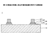
図1は、第1の実施の形態に係る半導体装置を例示する断面図である。図1を参照するに、半導体装置1は、半導体基板10と、電極パッド20と、突起電極30とを有する。
<First Embodiment>
[Structure of Semiconductor Device According to First Embodiment]
FIG. 1 is a cross-sectional view illustrating the semiconductor device according to the first embodiment. Referring to FIG. 1, the
半導体基板10は、例えば、薄板化された略円形状の半導体基板(ウェハ)が切断され個片化されたものである。半導体基板10の材料の一例としては、シリコン(Si)、ゲルマニウム(Ge)、ガリウムヒ素(GaAs)等を挙げることができるが、以下の説明はシリコン(Si)を例に行う。半導体基板10の厚さは、例えば50〜800μm程度とすることができる。
The
半導体基板10の電極パッド20側には半導体集積回路(図示せず)が形成されている。半導体集積回路(図示せず)は、半導体基板10に形成された拡散層(図示せず)、絶縁層(図示せず)、ビア(図示せず)、配線(図示せず)等から構成されている。なお、半導体基板10において、電極パッド20が形成されている側の面を、主面と称する場合がある。
A semiconductor integrated circuit (not shown) is formed on the
電極パッド20は、半導体基板10の主面上に設けられている。電極パッド20は、半導体集積回路(図示せず)に設けられた配線(図示せず)と電気的に接続されている。電極パッド20の材料としては、例えば、アルミニウム(Al)等を用いることができる。
The
電極パッド20の材料として、銅(Cu)層の上にアルミニウム(Al)層を形成したもの、銅(Cu)層の上にシリコン(Si)層を形成し、その上に更にアルミニウム(Al)層を形成したもの等を用いても構わない。電極パッド20の厚さは、例えば、10μm程度とすることができる。
As a material of the
なお、半導体基板10の主面に、電極パッド20を露出するように、保護膜を設けても構わない。保護膜としては、例えば、SiN膜、PSG膜等を用いることができる。又、SiN膜やPSG膜等からなる層に、更にポリイミド等からなる層を積層しても構わない。
A protective film may be provided on the main surface of the
突起電極30は、台座部31と、突起部32とを有し、電極パッド20と電気的に接続されている。台座部31は、電極パッド20上に設けられている。台座部31は、電極パッド20上の全面に設けてもよいし、電極パッド20の外周部を除く領域等に設けてもよい。台座部31は導電体であり、例えば、チタン(Ti)膜と銅(Cu)膜との積層構造とすることができる。この場合、チタン(Ti)膜の厚さは、例えば、0.1μm程度、銅(Cu)膜の厚さは、例えば、0.5μm程度とすることができる。台座部31は、クローム(Cr)膜と銅(Cu)膜との積層構造等としてもよい。台座部31は、例えば、円盤状に形成することができ、その場合の直径は、例えば、20〜50μm程度とすることができる。
The
突起部32は、台座部31上に設けられている。突起部32は、台座部31よりも小幅の柱状部33と、柱状部33の台座部31側の端部から台座部31に向かって徐々に拡幅するテーパ部34と、を備えている。換言すれば、柱状部33の平面形状は台座部31の平面形状よりも小さく形成されており、テーパ部34は、平面視において、柱状部33の外縁から環状に外方に突出している。又、テーパ部34の側面は、傾斜面である。なお、柱状部33とテーパ部34とは一体に形成されているが、便宜上、境界部(説明のために設けた境界)を破線で示している。
The
テーパ部34の側面の半導体基板20の主面に垂直な平面に対する傾斜角は、台座部31の側面の前記平面に対する傾斜角及び柱状部33の側面の前記平面に対する傾斜角よりも大きくされている。なお、台座部31の側面の前記平面に対する傾斜角及び柱状部33の側面の前記平面に対する傾斜角は、略0°である。つまり、台座部31の側面及び柱状部33の側面は、半導体基板20の主面に対して略垂直に形成されている。
The inclination angle of the side surface of the
柱状部33は、例えば、円柱状に形成することができる。この場合、柱状部33の直径は、例えば、20〜50μm程度とすることができる。但し、柱状部33の直径は、台座部31の直径よりも、数μm程度小さくなる。テーパ部34の平面形状は、例えば、円形とすることができる。この場合、テーパ部34の最小直径(柱状部33と連続する部分の直径)は柱状部33の直径と同一である。テーパ部34の最大直径(台座部31と接する部分の直径)は、例えば、柱状部33の直径プラス4μm程度とすることができる。この場合、テーパ部34は、平面視において、柱状部33の外縁から円環状に外方に突出し、柱状部33の外縁から外方に突出する部分の幅が2μm程度となる。
The
柱状部33及びテーパ部34は導電体であり、例えば、銅(Cu)等から構成することができる。柱状部33の高さは、テーパ部34の高さよりも高く形成されている。柱状部33の高さは、例えば、30μm程度とすることができる。テーパ部34の高さは、例えば、数μm程度とすることができる。なお、テーパ部34の傾斜面の断面形状は直線状であってもよいし、曲線状であってもよいし、直線と曲線とが混在していてもよい。又、柱状部33は、例えば、楕円柱状や角柱状としてもよいし、これに対応して、テーパ部34の平面形状は、例えば、楕円形や矩形としてもよい。
The
このように、突起電極30は、銅(Cu)を主成分として構成することができる。したがって、突起電極30を銅ピラーと称しても構わない。なお、図1では、突起電極30は図面を簡略化するために数量を減らして描かれているが、実際には、例えば、多数の突起電極30がペリフェラル状やエリアアレイ状に設けられている。突起電極30のピッチは、例えば30〜60μm程度とすることができる。
Thus, the protruding
[第1の実施の形態に係る半導体装置の製造方法]
次に、第1の実施の形態に係る半導体装置の製造方法について説明する。図2及び図3は、第1の実施の形態に係る半導体装置の製造工程を例示する図である。
[Method of Manufacturing Semiconductor Device According to First Embodiment]
Next, a method for manufacturing the semiconductor device according to the first embodiment will be described. 2 and 3 are diagrams illustrating the manufacturing process of the semiconductor device according to the first embodiment.
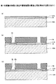
まず、図2(a)に示す工程では、略円形状の半導体基板10A(シリコンウェハ)を準備する。半導体基板10Aの直径は、例えば6インチ(約150mm)、8インチ(約200mm)、12インチ(約300mm)等とすることができる。又、半導体基板10Aの厚さは、例えば0.625mm(直径=6インチの場合)、0.725mm(直径=8インチの場合)、0.775mm(直径=12インチの場合)等とすることができる。
First, in the process shown in FIG. 2A, a substantially
次に、準備した半導体基板10Aの最終的に個片化されて半導体基板10となる複数の領域に、周知の手法により、各々半導体集積回路(図示せず)や電極パッド20等を形成する。電極パッド20の材料としては、例えば、アルミニウム(Al)等を用いることができる。
Next, a semiconductor integrated circuit (not shown), an
電極パッド20の材料として、銅(Cu)層の上にアルミニウム(Al)層を形成したもの、銅(Cu)層の上にシリコン(Si)層を形成し、その上に更にアルミニウム(Al)層を形成したもの等を用いても構わない。電極パッド20の厚さは、例えば、10μm程度とすることができる。
As a material of the
次に、半導体基板10となる複数の領域の各主面上に、電極パッド20を被覆する金属層31Aを形成する。金属層31Aは、例えば、チタン(Ti)膜と銅(Cu)膜との積層構造とすることができる。この場合、電極パッド20上のチタン(Ti)膜の厚さは、例えば、0.1μm程度、電極パッド20上の銅(Cu)膜の厚さは、例えば、0.5μm程度とすることができる。金属層31Aは、例えば、スパッタ法等により形成できる。金属層31Aは、クローム(Cr)膜と銅(Cu)膜との積層構造等としてもよい。なお、金属層31Aは、最終的にエッチングされて台座部31となる部分である。
Next, a
なお、図2(a)〜図3(c)は、半導体基板10Aの最終的に個片化されて半導体基板10となる複数の領域(半導体装置1となる複数の領域)の内の1つのみを図示している。
2A to FIG. 3C show one of a plurality of regions (a plurality of regions that become the semiconductor device 1) that are finally separated into pieces of the
次に、図2(b)に示す工程では、金属層31A上に液状又はペースト状のレジストを塗布して、又は、フィルム状のレジスト(ドライフィルムレジスト等)をラミネートしてレジスト層50を形成する。そして、塗布又はラミネートしたレジスト層50を露光及び現像することで突起電極30の形成位置に対応する部分に開口部55を形成する。
Next, in the step shown in FIG. 2B, a resist
開口部55は、例えば、ペリフェラル状やエリアアレイ状に形成できる。開口部55の平面形状は、例えば、円形とすることができる。開口部55の平面形状が円形である場合、その直径は、例えば、20〜50μm程度とすることができる。開口部55のピッチは、例えば30〜60μm程度とすることができる。
The
次に、図2(c)に示す工程では、各開口部55内に薬液を供給し、薬液により各開口部55内に露出するレジスト層50の金属層31A側の端部(各開口部55内に露出するレジスト層50の根元部分)を溶解して環状の切れ込み部55xを形成する。切れ込み部55xは、各開口部55内に露出するレジスト層50の金属層31A側の端部に、金属層31A側に向かって徐々に拡幅するテーパ状に形成される。
Next, in the step shown in FIG. 2C, a chemical solution is supplied into each
つまり、切れ込み部55xの内側面は、傾斜面とされている。切れ込み部55xの最大直径(金属層31Aと接する部分の直径)は、例えば、開口部55の切れ込み部55xが形成されていない部分の直径プラス4μm程度とすることができる。切れ込み部55xの最高部の高さ(金属層31A表面からの高さ)は、例えば、数μm程度とすることができる。
That is, the inner surface of the
薬液としては、レジスト層50を溶解できればどのような溶液を用いても構わないが、例えば、弱酸性に調整された溶液を用いることができる。弱酸性に調整された溶液の一例としては、濃度が5%以下の硫酸水溶液等を挙げることができる。この溶液は、特にレジスト層50としてドライフィルムレジストを用いた場合に有効である。薬液の供給は、例えば、ノズルから滴下することにより行ってもよいし、スプレーから所定の圧力で吹き付けることにより行ってもよいし、その他の方法により行ってもよい。
As the chemical solution, any solution may be used as long as the resist
次に、図3(a)に示す工程では、切れ込み部55xを含む各開口部55内に金属を充填し、各開口部55内に露出する金属層31A上に、柱状部33及びテーパ部34を含む突起部32を形成する。突起部32は、例えば、金属層31Aを給電層として利用する電解めっき法等により形成できる。柱状部33及びテーパ部34の材料としては、例えば、銅(Cu)等を用いることができる。この工程により、切れ込み部55xに形成されたテーパ部34と、テーパ部34上にテーパ部34と一体に形成された柱状部33とを含む突起部32が形成される。なお、突起部32の高さは、例えば、30μm程度とすることができる。
Next, in the step shown in FIG. 3A, each opening 55 including the
次に、図3(b)に示す工程では、図3(a)に示すレジスト層50を除去する。そして、図3(c)に示す工程では、突起部32をマスクとして図3(b)に示す金属層31Aの不要部分をエッチングにより除去し、電極パッド20とテーパ部34との間に台座部31を形成する。この工程により、台座部31と突起部32(柱状部33及びテーパ部34)とを備えた突起電極30が形成される。
Next, in the step shown in FIG. 3B, the resist
図3(c)に示す工程において、テーパ部34の側面の半導体基板20の主面に垂直な平面に対する傾斜角は、台座部31の側面の前記平面に対する傾斜角及び柱状部33の側面の前記平面に対する傾斜角よりも大きく形成される。又、台座部31の側面及び柱状部33の側面は、半導体基板20の主面に対して略垂直に形成される。
In the step shown in FIG. 3C, the inclination angle of the side surface of the tapered
図3(c)に示す工程において、金属層31Aの不要部分をエッチングにより除去する際に、突起部32のテーパ部34が傘となるため、金属層31Aが過剰にエッチングされることはない。そのため、突起電極30の根元部分がくびれることを防止できる。より詳しくは、突起電極30において、台座部31の幅が柱状部33の幅よりも狭くなることを防止できる。
In the step shown in FIG. 3C, when the unnecessary portion of the
図3(c)に示す工程の後、半導体基板10Aをダイシング等により個片化することにより、図1に示す半導体装置1が複数個作製される。
After the step shown in FIG. 3C, the
このように、第1の実施の形態では、金属層31A上に開口部55内を備えたレジスト層50を形成し、開口部55内に露出するレジスト層50の金属層31A側の端部を溶解して環状の切れ込み部55xを形成する。そして、切れ込み部55xを含む開口部55内に金属を充填し、柱状部33及びテーパ部34を含む突起部32を形成する。そして、レジスト層50を除去後、突起部32をマスクとして金属層31Aをエッチングし、電極パッド20とテーパ部34との間に台座部31を形成して、台座部31と突起部32とを備えた突起電極30を形成する。
As described above, in the first embodiment, the resist
これにより、金属層31Aをエッチングする工程において、突起部32のテーパ部34が傘となり、金属層31Aが過剰にエッチングされないため、突起電極30の根元部分がくびれることを防止できる。より詳しくは、突起電極30において、台座部31の幅が柱状部33の幅よりも狭くなることを防止できる。
Thereby, in the step of etching the
突起電極の根元部分がくびれると、特に、突起電極の小径化、狭ピッチ化が進んだ際に、接続信頼性が低下する問題が生じる。例えば、半導体装置が高温下や低温下で繰り返し使用された場合の熱ストレスにより、突起電極の根元部分(くびれた部分)にクラックが入ったり断線したりする問題が生じる。 When the base portion of the protruding electrode is constricted, there is a problem that the connection reliability is lowered particularly when the diameter and the pitch of the protruding electrode are reduced. For example, there is a problem that the base portion (constricted portion) of the protruding electrode is cracked or disconnected due to thermal stress when the semiconductor device is repeatedly used at high or low temperatures.
第1の実施の形態に係る半導体装置1では、突起電極30の根元部分がくびれることを防止できるため、突起電極30の小径化、狭ピッチ化が進んだ場合でも、接続信頼性を確保できる。
In the
〈第1の実施の形態の変形例〉
第1の実施の形態の変形例では、第1の実施の形態とは異なる方法により切れ込み部55xを形成する例を示す。なお、第1の実施の形態の変形例において、既に説明した実施の形態と同一構成部品についての説明は省略する。
<Modification of First Embodiment>
In the modification of the first embodiment, an example in which the
ドライフィルムレジストは、アクリル系共重合体とアクリレートモノマーとを主成分として含んでおり、水に対して微溶解である。そこで、図2(b)に示す工程において、レジスト層50としてドライフィルムレジストを用いた場合には、図2(c)に示す工程において、各開口部55内に水を供給してもよい。各開口部55内に水を供給することにより、各開口部55内に露出するレジスト層50の金属層31A側の端部を膨潤剥離で浮き上がらせて切れ込み部55xを形成できる。なお、水に対して微溶解であれば、ドライフィルムレジスト以外のレジストを用いても構わない。
The dry film resist contains an acrylic copolymer and an acrylate monomer as main components and is slightly soluble in water. Therefore, when a dry film resist is used as the resist
各開口部55内に露出するレジスト層50の金属層31A側の端部を膨潤剥離で浮き上がらせるためには、各開口部55内に露出するレジスト層50の金属層31A側の端部を、例えば、数時間程度水に浸漬させる必要がある。但し、所定の水圧で各開口部55内に露出するレジスト層50の金属層31A側の端部を叩くことにより、切れ込み部55xの形成時間を短縮することができる。
In order to lift the end of the resist
このように、レジスト層50として水に対して微溶解のレジストを用い、各開口部55内に露出するレジスト層50の金属層31A側の端部を水に浸漬させ、各開口部55の下端側を膨潤剥離で浮き上がらせて切れ込み部55xを形成してもよい。この場合にも、第1の実施の形態と同様の効果を奏する。
As described above, a resist that is slightly soluble in water is used as the resist
〈第2の実施の形態〉
第2の実施の形態では、本発明を配線基板に適用する例を示す。なお、第2の実施の形態において、既に説明した実施の形態と同一構成部品についての説明は省略する。
<Second Embodiment>
In the second embodiment, an example in which the present invention is applied to a wiring board will be described. In the second embodiment, the description of the same components as those of the already described embodiments is omitted.
図4は、第2の実施の形態に係る配線基板を例示する断面図である。図2を参照するに、配線基板2は、絶縁性部材70と、電極パッド80と、突起電極30とを有する。
FIG. 4 is a cross-sectional view illustrating a wiring board according to the second embodiment. Referring to FIG. 2, the
絶縁性部材70は、例えば、ガラスクロスにエポキシ系樹脂を含浸させた部材である。絶縁性部材70の厚さは、例えば、数100μm程度とすることができる。電極パッド80は、絶縁性部材70の主面上に設けられている。電極パッド80は、絶縁性部材70の主面上に形成された配線パターン(図示せず)と電気的に接続されている。電極パッド80の材料としては、例えば、銅(Cu)等を用いることができる。電極パッド80の厚さは、例えば、10μm程度とすることができる。
The insulating
なお、絶縁性部材70の主面上に、電極パッド80を露出するソルダーレジスト層を設けてもよい。ソルダーレジスト層としては、例えば、感光性のエポキシ系絶縁性樹脂等を用いることができる。又、絶縁性部材70の主面とは反対側の面上にも配線パターンを設け、絶縁性部材70を貫通するスルーホールを介して、主面上に形成された配線パターンと電気的に接続してもよい。又、絶縁性部材70の主面上又はその反対側の面上の何れか一方又は双方に、多層化された配線パターンを形成してもよい。
A solder resist layer that exposes the
電極パッド80上には、第1の実施の形態と同様の突起電極30が形成されている。配線基板2において、突起電極30は、第1の実施の形態と同様の方法により形成できる。但し、図2(a)に示す工程で形成する金属層31Aの材料として、銅(Cu)等を用いることができる。又、金属層31Aは、例えば、無電解めっき法等により形成できる。
On the
このように、配線基板2に突起電極30を形成した場合にも、第1の実施の形態と同様の効果を奏する。
As described above, even when the protruding
以上、好ましい実施の形態及びその変形例について詳説したが、上述した実施の形態及びその変形例に制限されることはなく、特許請求の範囲に記載された範囲を逸脱することなく、上述した実施の形態及びその変形例に種々の変形及び置換を加えることができる。 The preferred embodiment and its modification have been described in detail above, but the present invention is not limited to the above-described embodiment and its modification, and the above-described implementation is performed without departing from the scope described in the claims. Various modifications and substitutions can be added to the embodiment and its modifications.
例えば、第2の実施の形態において、第1の実施の形態の変形例と同様の変形を加えてもよい。 For example, in the second embodiment, a modification similar to the modification of the first embodiment may be added.
1 半導体装置
2 配線基板
10、10A 半導体基板
20、80 電極パッド
30 突起電極
31 台座部
31A 金属層
32 突起部
33 柱状部
34 テーパ部
50 レジスト層
55 開口部
55x 切れ込み部
70 絶縁性部材
DESCRIPTION OF
Claims (12)
前記半導体基板の主面に形成された電極パッドと、
前記電極パッドと電気的に接続された突起電極と、を有し、
前記突起電極は、前記電極パッド上に設けられた台座部と、前記台座部上に設けられた突起部と、を備え、
前記台座部は、上層が銅膜から形成された積層構造であり、
前記突起部は、前記台座部よりも小幅の柱状部と、前記柱状部の前記台座部側の端部から前記台座部に向かって徐々に拡幅するテーパ部と、を備え、
前記柱状部と前記テーパ部とは一体に形成されており、
前記柱状部の高さは、前記テーパ部の高さよりも高く、
前記柱状部の上面は外部に露出しており、
前記テーパ部側面の前記主面に垂直な平面に対する傾斜角は、前記台座部側面の前記平面に対する傾斜角及び前記柱状部側面の前記平面に対する傾斜角よりも大きい半導体装置。 A semiconductor substrate;
An electrode pad formed on the main surface of the semiconductor substrate;
A protruding electrode electrically connected to the electrode pad,
The protruding electrode includes a pedestal portion provided on the electrode pad, and a protruding portion provided on the pedestal portion,
The pedestal portion has a laminated structure in which an upper layer is formed from a copper film,
The protruding portion includes a columnar portion having a width smaller than that of the pedestal portion, and a tapered portion that gradually widens from the end portion on the pedestal portion side of the columnar portion toward the pedestal portion,
The columnar portion and the tapered portion are formed integrally,
The height of the columnar portion is higher than the height of the tapered portion,
The upper surface of the columnar part is exposed to the outside,
The inclination angle of the tapered portion side surface with respect to a plane perpendicular to the main surface is larger than the inclination angle of the pedestal portion side surface with respect to the plane and the inclination angle of the columnar portion side surface with respect to the plane.
前記絶縁性部材の主面に形成された電極パッドと、
前記電極パッドと電気的に接続された突起電極と、を有し、
前記突起電極は、前記電極パッド上に設けられた台座部と、前記台座部上に設けられた突起部と、を備え、
前記台座部は、上層が銅膜から形成された積層構造であり、
前記突起部は、前記台座部よりも小幅の柱状部と、前記柱状部の前記台座部側の端部から前記台座部に向かって徐々に拡幅するテーパ部と、を備え、
前記柱状部と前記テーパ部とは一体に形成されており、
前記柱状部の高さは、前記テーパ部の高さよりも高く、
前記柱状部の上面は外部に露出しており、
前記テーパ部側面の前記主面に垂直な平面に対する傾斜角は、前記台座部側面の前記平面に対する傾斜角及び前記柱状部側面の前記平面に対する傾斜角よりも大きい配線基板。 An insulating member;
An electrode pad formed on the main surface of the insulating member;
A protruding electrode electrically connected to the electrode pad,
The protruding electrode includes a pedestal portion provided on the electrode pad, and a protruding portion provided on the pedestal portion,
The pedestal portion has a laminated structure in which an upper layer is formed from a copper film,
The protruding portion includes a columnar portion having a width smaller than that of the pedestal portion, and a tapered portion that gradually widens from the end portion on the pedestal portion side of the columnar portion toward the pedestal portion,
The columnar portion and the tapered portion are formed integrally,
The height of the columnar portion is higher than the height of the tapered portion,
The upper surface of the columnar part is exposed to the outside,
The wiring board is configured such that an inclination angle of the side surface of the tapered portion with respect to a plane perpendicular to the main surface is larger than an inclination angle of the side surface of the pedestal portion with respect to the plane and an inclination angle of the side surface of the columnar portion with respect to the plane.
前記電極パッドと電気的に接続された突起電極を形成する工程と、を有し、
前記突起電極を形成する工程は、
前記半導体基板の主面に前記電極パッドを被覆する金属層を形成する工程と、
前記金属層上に、前記突起電極の形成位置に対応する部分に開口部を備えたレジスト層を形成する工程と、
前記開口部内に露出する前記レジスト層の前記金属層側の端部に環状の切れ込み部を形成する工程と、
前記切れ込み部を含む前記開口部内に金属を充填し、前記切れ込み部に形成されたテーパ部と、前記テーパ部上に前記テーパ部と一体に形成された前記テーパ部の高さよりも高い柱状部と、を含む突起部を形成する工程と、
前記レジスト層を除去後、前記突起部をマスクとして前記金属層をエッチングし、前記電極パッドと前記テーパ部との間に台座部を形成して、前記台座部と前記突起部とを備えた前記突起電極を形成する工程と、を含む半導体装置の製造方法。 Forming electrode pads on the main surface of the semiconductor substrate;
Forming a protruding electrode electrically connected to the electrode pad,
The step of forming the protruding electrode includes:
Forming a metal layer covering the electrode pad on the main surface of the semiconductor substrate;
On the metal layer, forming a resist layer having an opening in a portion corresponding to the formation position of the protruding electrode;
Forming an annular cut at the metal layer side end of the resist layer exposed in the opening;
The opening including the cut portion is filled with metal, a tapered portion formed in the cut portion, and a columnar portion higher than the height of the tapered portion formed integrally with the tapered portion on the tapered portion; Forming a protrusion including:
After removing the resist layer, the metal layer is etched using the protrusion as a mask, a pedestal is formed between the electrode pad and the taper, and the pedestal and the protrusion are provided. Forming a protruding electrode; and a method of manufacturing a semiconductor device.
前記電極パッドと電気的に接続された突起電極を形成する工程と、を有し、
前記突起電極を形成する工程は、
前記絶縁性部材の主面に前記電極パッドを被覆する金属層を形成する工程と、
前記金属層上に、前記突起電極の形成位置に対応する部分に開口部を備えたレジスト層を形成する工程と、
前記開口部内に露出する前記レジスト層の前記金属層側の端部に環状の切れ込み部を形成する工程と、
前記切れ込み部を含む前記開口部内に金属を充填し、前記切れ込み部に形成されたテーパ部と、前記テーパ部上に前記テーパ部と一体に形成された前記テーパ部の高さよりも高い柱状部と、を含む突起部を形成する工程と、
前記レジスト層を除去後、前記突起部をマスクとして前記金属層をエッチングし、前記電極パッドと前記テーパ部との間に台座部を形成して、前記台座部と前記突起部とを備えた前記突起電極を形成する工程と、を含む配線基板の製造方法。 Forming an electrode pad on the main surface of the insulating member;
Forming a protruding electrode electrically connected to the electrode pad,
The step of forming the protruding electrode includes:
Forming a metal layer covering the electrode pad on the main surface of the insulating member;
On the metal layer, forming a resist layer having an opening in a portion corresponding to the formation position of the protruding electrode;
Forming an annular cut at the metal layer side end of the resist layer exposed in the opening;
The opening including the cut portion is filled with metal, a tapered portion formed in the cut portion, and a columnar portion higher than the height of the tapered portion formed integrally with the tapered portion on the tapered portion; Forming a protrusion including:
After removing the resist layer, the metal layer is etched using the protrusion as a mask, a pedestal is formed between the electrode pad and the taper, and the pedestal and the protrusion are provided. Forming a protruding electrode; and a method of manufacturing a wiring board.
Priority Applications (2)
| Application Number | Priority Date | Filing Date | Title |
|---|---|---|---|
| JP2012138474A JP6154995B2 (en) | 2012-06-20 | 2012-06-20 | Semiconductor device, wiring board, and manufacturing method thereof |
| US13/920,336 US9082672B2 (en) | 2012-06-20 | 2013-06-18 | Semiconductor device and method of manufacturing the same, and wiring substrate and method of manufacturing the same |
Applications Claiming Priority (1)
| Application Number | Priority Date | Filing Date | Title |
|---|---|---|---|
| JP2012138474A JP6154995B2 (en) | 2012-06-20 | 2012-06-20 | Semiconductor device, wiring board, and manufacturing method thereof |
Publications (3)
| Publication Number | Publication Date |
|---|---|
| JP2014003201A JP2014003201A (en) | 2014-01-09 |
| JP2014003201A5 JP2014003201A5 (en) | 2015-07-23 |
| JP6154995B2 true JP6154995B2 (en) | 2017-06-28 |
Family
ID=49773731
Family Applications (1)
| Application Number | Title | Priority Date | Filing Date |
|---|---|---|---|
| JP2012138474A Active JP6154995B2 (en) | 2012-06-20 | 2012-06-20 | Semiconductor device, wiring board, and manufacturing method thereof |
Country Status (2)
| Country | Link |
|---|---|
| US (1) | US9082672B2 (en) |
| JP (1) | JP6154995B2 (en) |
Families Citing this family (3)
| Publication number | Priority date | Publication date | Assignee | Title |
|---|---|---|---|---|
| JP7117615B2 (en) * | 2017-12-08 | 2022-08-15 | パナソニックIpマネジメント株式会社 | Semiconductor device manufacturing method |
| JP7357243B2 (en) * | 2019-04-18 | 2023-10-06 | パナソニックIpマネジメント株式会社 | Semiconductor device, mounting structure of semiconductor device, and manufacturing method of semiconductor device |
| JP2021093417A (en) * | 2019-12-09 | 2021-06-17 | イビデン株式会社 | Print circuit board and manufacturing method of print circuit board |
Family Cites Families (10)
| Publication number | Priority date | Publication date | Assignee | Title |
|---|---|---|---|---|
| JP3015436B2 (en) * | 1990-09-25 | 2000-03-06 | 株式会社東芝 | Semiconductor device and connection method thereof |
| SG71734A1 (en) * | 1997-11-21 | 2000-04-18 | Inst Materials Research & Eng | Area array stud bump flip chip and assembly process |
| JP4403631B2 (en) * | 2000-04-24 | 2010-01-27 | ソニー株式会社 | Manufacturing method of chip-shaped electronic component and manufacturing method of pseudo wafer used for manufacturing the same |
| US6940178B2 (en) * | 2001-02-27 | 2005-09-06 | Chippac, Inc. | Self-coplanarity bumping shape for flip chip |
| JP3851517B2 (en) * | 2001-04-18 | 2006-11-29 | カシオマイクロニクス株式会社 | Semiconductor device, method of manufacturing the same, and junction structure thereof |
| JP2004200247A (en) * | 2002-12-16 | 2004-07-15 | Seiko Epson Corp | Terminal, forming method therefor, semiconductor chip, semiconductor mounting substrate, electronic device and electronic apparatus |
| JP2005116632A (en) * | 2003-10-03 | 2005-04-28 | Rohm Co Ltd | Semiconductor device and manufacturing method thereof |
| JP2007073919A (en) * | 2005-09-06 | 2007-03-22 | Tanemasa Asano | Method of manufacturing bump electrode, baking apparatus used therefor, and electronic device |
| US7713782B2 (en) * | 2006-09-22 | 2010-05-11 | Stats Chippac, Inc. | Fusible I/O interconnection systems and methods for flip-chip packaging involving substrate-mounted stud-bumps |
| JP5865630B2 (en) * | 2011-08-23 | 2016-02-17 | 京セラ株式会社 | Electrode structure, semiconductor element, semiconductor device, thermal head, and thermal printer |
-
2012
- 2012-06-20 JP JP2012138474A patent/JP6154995B2/en active Active
-
2013
- 2013-06-18 US US13/920,336 patent/US9082672B2/en active Active
Also Published As
| Publication number | Publication date |
|---|---|
| US9082672B2 (en) | 2015-07-14 |
| JP2014003201A (en) | 2014-01-09 |
| US20130341788A1 (en) | 2013-12-26 |
Similar Documents
| Publication | Publication Date | Title |
|---|---|---|
| KR100956229B1 (en) | Semiconductor device having projecting electrode formed by electrolytic plating, and manufacturing method thereof | |
| JP2002076047A (en) | Bump forming method, semiconductor device and its manufacturing method, circuit board and electronic equipment | |
| US7132358B2 (en) | Method of forming solder bump with reduced surface defects | |
| JP2008047652A (en) | Semiconductor device and method of manufacturing the same | |
| JP2010238702A (en) | Method for manufacturing semiconductor package and semiconductor package | |
| TW201325341A (en) | Wiring substrate and method of manufacturing the same | |
| US10446515B2 (en) | Semiconductor substrate and semiconductor packaging device, and method for forming the same | |
| JP2003203940A (en) | Semiconductor chip and wiring base board and manufacturing method of them, semiconductor wafer, semiconductor device, circuit base board and electronic instrument | |
| JP2015056458A (en) | Semiconductor device | |
| KR101708535B1 (en) | Integrated circuit apparatus and method for manufacturing the same | |
| JP6154995B2 (en) | Semiconductor device, wiring board, and manufacturing method thereof | |
| JP2002203869A (en) | Forming method of bump, semiconductor device, method for manufacturing the device, circuit substrate and electronic equipment | |
| JP6619294B2 (en) | WIRING BOARD, MANUFACTURING METHOD THEREOF, AND ELECTRONIC COMPONENT DEVICE | |
| US9524944B2 (en) | Method for fabricating package structure | |
| US10643934B2 (en) | Wiring substrate and electronic component device | |
| JP2003282790A (en) | Semiconductor device, its manufacturing method, circuit board, and electronic apparatus | |
| JPH11224890A (en) | Semiconductor device and its manufacturing | |
| JP2009231402A (en) | Semiconductor device, and manufacturing method of semiconductor device | |
| JP4949790B2 (en) | Manufacturing method of semiconductor device | |
| JP2001148393A (en) | Bump forming method, semiconductor device and its manufacturing method, wiring board, and electronic equipment | |
| US11749596B2 (en) | Wiring substrate | |
| JP5022963B2 (en) | Projection electrode structure, element mounting substrate and manufacturing method thereof, semiconductor module, and portable device | |
| JP2007250849A (en) | Method of manufacturing semiconductor device | |
| JP4971960B2 (en) | Manufacturing method of semiconductor device | |
| JP2004281614A (en) | Method for manufacturing semiconductor device |
Legal Events
| Date | Code | Title | Description |
|---|---|---|---|
| A521 | Written amendment |
Free format text: JAPANESE INTERMEDIATE CODE: A523 Effective date: 20150608 |
|
| A621 | Written request for application examination |
Free format text: JAPANESE INTERMEDIATE CODE: A621 Effective date: 20150608 |
|
| A977 | Report on retrieval |
Free format text: JAPANESE INTERMEDIATE CODE: A971007 Effective date: 20160304 |
|
| A131 | Notification of reasons for refusal |
Free format text: JAPANESE INTERMEDIATE CODE: A131 Effective date: 20160405 |
|
| A521 | Written amendment |
Free format text: JAPANESE INTERMEDIATE CODE: A523 Effective date: 20160603 |
|
| A131 | Notification of reasons for refusal |
Free format text: JAPANESE INTERMEDIATE CODE: A131 Effective date: 20161108 |
|
| A521 | Written amendment |
Free format text: JAPANESE INTERMEDIATE CODE: A523 Effective date: 20161222 |
|
| TRDD | Decision of grant or rejection written | ||
| A01 | Written decision to grant a patent or to grant a registration (utility model) |
Free format text: JAPANESE INTERMEDIATE CODE: A01 Effective date: 20170516 |
|
| A61 | First payment of annual fees (during grant procedure) |
Free format text: JAPANESE INTERMEDIATE CODE: A61 Effective date: 20170605 |
|
| R150 | Certificate of patent or registration of utility model |
Ref document number: 6154995 Country of ref document: JP Free format text: JAPANESE INTERMEDIATE CODE: R150 |