JP6147177B2 - Antenna cover and plasma generator using the same - Google Patents
Antenna cover and plasma generator using the same Download PDFInfo
- Publication number
- JP6147177B2 JP6147177B2 JP2013256014A JP2013256014A JP6147177B2 JP 6147177 B2 JP6147177 B2 JP 6147177B2 JP 2013256014 A JP2013256014 A JP 2013256014A JP 2013256014 A JP2013256014 A JP 2013256014A JP 6147177 B2 JP6147177 B2 JP 6147177B2
- Authority
- JP
- Japan
- Prior art keywords
- antenna
- antenna cover
- thickness
- plasma
- terminal
- Prior art date
- Legal status (The legal status is an assumption and is not a legal conclusion. Google has not performed a legal analysis and makes no representation as to the accuracy of the status listed.)
- Active
Links
Images


Classifications
-
- H—ELECTRICITY
- H01—ELECTRIC ELEMENTS
- H01Q—ANTENNAS, i.e. RADIO AERIALS
- H01Q1/00—Details of, or arrangements associated with, antennas
- H01Q1/40—Radiating elements coated with or embedded in protective material
-
- H—ELECTRICITY
- H05—ELECTRIC TECHNIQUES NOT OTHERWISE PROVIDED FOR
- H05H—PLASMA TECHNIQUE; PRODUCTION OF ACCELERATED ELECTRICALLY-CHARGED PARTICLES OR OF NEUTRONS; PRODUCTION OR ACCELERATION OF NEUTRAL MOLECULAR OR ATOMIC BEAMS
- H05H1/00—Generating plasma; Handling plasma
- H05H1/24—Generating plasma
- H05H1/46—Generating plasma using applied electromagnetic fields, e.g. high frequency or microwave energy
-
- H—ELECTRICITY
- H01—ELECTRIC ELEMENTS
- H01J—ELECTRIC DISCHARGE TUBES OR DISCHARGE LAMPS
- H01J37/00—Discharge tubes with provision for introducing objects or material to be exposed to the discharge, e.g. for the purpose of examination or processing thereof
- H01J37/32—Gas-filled discharge tubes
- H01J37/32009—Arrangements for generation of plasma specially adapted for examination or treatment of objects, e.g. plasma sources
- H01J37/32082—Radio frequency generated discharge
- H01J37/321—Radio frequency generated discharge the radio frequency energy being inductively coupled to the plasma
- H01J37/3211—Antennas, e.g. particular shapes of coils
-
- H—ELECTRICITY
- H01—ELECTRIC ELEMENTS
- H01L—SEMICONDUCTOR DEVICES NOT COVERED BY CLASS H10
- H01L21/00—Processes or apparatus adapted for the manufacture or treatment of semiconductor or solid state devices or of parts thereof
- H01L21/02—Manufacture or treatment of semiconductor devices or of parts thereof
- H01L21/04—Manufacture or treatment of semiconductor devices or of parts thereof the devices having at least one potential-jump barrier or surface barrier, e.g. PN junction, depletion layer or carrier concentration layer
- H01L21/18—Manufacture or treatment of semiconductor devices or of parts thereof the devices having at least one potential-jump barrier or surface barrier, e.g. PN junction, depletion layer or carrier concentration layer the devices having semiconductor bodies comprising elements of Group IV of the Periodic System or AIIIBV compounds with or without impurities, e.g. doping materials
- H01L21/26—Bombardment with radiation
- H01L21/263—Bombardment with radiation with high-energy radiation
- H01L21/265—Bombardment with radiation with high-energy radiation producing ion implantation
-
- H—ELECTRICITY
- H01—ELECTRIC ELEMENTS
- H01Q—ANTENNAS, i.e. RADIO AERIALS
- H01Q1/00—Details of, or arrangements associated with, antennas
- H01Q1/42—Housings not intimately mechanically associated with radiating elements, e.g. radome
-
- H—ELECTRICITY
- H01—ELECTRIC ELEMENTS
- H01Q—ANTENNAS, i.e. RADIO AERIALS
- H01Q1/00—Details of, or arrangements associated with, antennas
- H01Q1/42—Housings not intimately mechanically associated with radiating elements, e.g. radome
- H01Q1/421—Means for correcting aberrations introduced by a radome
-
- H—ELECTRICITY
- H01—ELECTRIC ELEMENTS
- H01Q—ANTENNAS, i.e. RADIO AERIALS
- H01Q7/00—Loop antennas with a substantially uniform current distribution around the loop and having a directional radiation pattern in a plane perpendicular to the plane of the loop
-
- H—ELECTRICITY
- H05—ELECTRIC TECHNIQUES NOT OTHERWISE PROVIDED FOR
- H05H—PLASMA TECHNIQUE; PRODUCTION OF ACCELERATED ELECTRICALLY-CHARGED PARTICLES OR OF NEUTRONS; PRODUCTION OR ACCELERATION OF NEUTRAL MOLECULAR OR ATOMIC BEAMS
- H05H1/00—Generating plasma; Handling plasma
- H05H1/24—Generating plasma
- H05H1/46—Generating plasma using applied electromagnetic fields, e.g. high frequency or microwave energy
- H05H1/461—Microwave discharges
-
- H—ELECTRICITY
- H05—ELECTRIC TECHNIQUES NOT OTHERWISE PROVIDED FOR
- H05H—PLASMA TECHNIQUE; PRODUCTION OF ACCELERATED ELECTRICALLY-CHARGED PARTICLES OR OF NEUTRONS; PRODUCTION OR ACCELERATION OF NEUTRAL MOLECULAR OR ATOMIC BEAMS
- H05H1/00—Generating plasma; Handling plasma
- H05H1/24—Generating plasma
- H05H1/46—Generating plasma using applied electromagnetic fields, e.g. high frequency or microwave energy
- H05H1/4645—Radiofrequency discharges
- H05H1/4652—Radiofrequency discharges using inductive coupling means, e.g. coils
Description
本発明は、プラズマ発生装置のアンテナを保護するアンテナカバーに関する。 The present invention relates to an antenna cover for protecting an antenna of a plasma generator.
プラズマ発生装置では、例えば、プラズマ室内のアンテナ近傍に生じるRF電界により、プラズマ電子を加速してプラズマを生成する。このとき、アンテナがプラズマに曝されると、アンテナがスパッタされプラズマの汚染原因となることから、発生するプラズマからアンテナを保護する部材が設けられる。例えば、プラズマ室とアンテナ室との間に仕切り板を設けることによりアンテナが保護される(例えば、特許文献1参照) In the plasma generator, for example, plasma electrons are accelerated by an RF electric field generated in the vicinity of an antenna in the plasma chamber to generate plasma. At this time, if the antenna is exposed to plasma, the antenna is sputtered and causes plasma contamination. Therefore, a member for protecting the antenna from the generated plasma is provided. For example, the antenna is protected by providing a partition plate between the plasma chamber and the antenna chamber (see, for example, Patent Document 1).
アンテナの保護部材はプラズマに曝されるため、プラズマにより損傷を受けることとなる。仮に、プラズマの影響により消耗されて保護部材に穴があいてしまうと、アンテナが露出してプラズマが汚染されてしまう。保護部材を厚くしたり、プラズマの発生位置からアンテナや保護部材を遠ざけたりすれば、保護部材の消耗を低減させることができるが、プラズマを生成する効率の低下につながる。 Since the protective member of the antenna is exposed to the plasma, it is damaged by the plasma. If the protective member has a hole due to the influence of plasma, the antenna is exposed and the plasma is contaminated. If the protective member is thickened or the antenna or the protective member is moved away from the plasma generation position, the consumption of the protective member can be reduced, but the efficiency of generating plasma is reduced.
本発明のある態様の例示的な目的のひとつは、プラズマの生成効率を維持しつつ、プラズマによる消耗の影響を低減させたアンテナカバー及びそれを用いたプラズマ発生装置を提供することにある。 One exemplary object of an aspect of the present invention is to provide an antenna cover that reduces the influence of plasma consumption while maintaining plasma generation efficiency, and a plasma generator using the antenna cover.
本発明のある態様によると、プラズマ室の内部に設けられ、当該プラズマ室内に高周波を放射するアンテナの表面を保護するアンテナカバーが提供される。アンテナカバーは、当該アンテナカバーの外表面における電位の空間依存性が低減されるように、アンテナの表面に直交する方向のうち少なくとも一方向におけるアンテナカバーの厚さが、当該表面上の位置に応じて異なる。 According to an aspect of the present invention, there is provided an antenna cover that is provided inside a plasma chamber and protects the surface of the antenna that radiates a high frequency into the plasma chamber. For the antenna cover, the thickness of the antenna cover in at least one direction orthogonal to the antenna surface depends on the position on the surface so that the spatial dependence of the potential on the outer surface of the antenna cover is reduced. Different.
本発明のある態様によると、プラズマ発生装置が提供される。本装置は、プラズマ室と、プラズマ室の内部に磁場を印加する磁石と、プラズマ室の内部に設けられ、当該プラズマ室内に高周波を放射するアンテナと、アンテナの表面を保護するアンテナカバーと、を備える。アンテナカバーは、当該アンテナカバーの外表面における電位の空間依存性が低減されるように、アンテナの表面に直交する方向のうち少なくとも一方向におけるアンテナカバーの厚さが、当該表面上の位置に応じて異なる。 According to an aspect of the present invention, a plasma generator is provided. The apparatus includes a plasma chamber, a magnet that applies a magnetic field to the inside of the plasma chamber, an antenna that is provided inside the plasma chamber and radiates high frequency into the plasma chamber, and an antenna cover that protects the surface of the antenna. Prepare. For the antenna cover, the thickness of the antenna cover in at least one of the directions orthogonal to the antenna surface depends on the position on the surface so that the spatial dependence of the potential on the outer surface of the antenna cover is reduced. Different.
なお、以上の構成要素の任意の組み合わせや本発明の構成要素や表現を、方法、装置、システムなどの間で相互に置換したものもまた、本発明の態様として有効である。 Note that any combination of the above-described constituent elements and the constituent elements and expressions of the present invention replaced with each other among methods, apparatuses, systems, and the like are also effective as an aspect of the present invention.
本発明によれば、プラズマの生成効率を維持しつつ、プラズマによる消耗の影響を低減させたアンテナカバー及びそれを用いたプラズマ発生装置を提供することができる。 According to the present invention, it is possible to provide an antenna cover and a plasma generator using the antenna cover in which the influence of plasma consumption is reduced while maintaining plasma generation efficiency.
以下、図面を参照しながら、本発明を実施するための形態について詳細に説明する。なお、図面の説明において同一の要素には同一の符号を付し、重複する説明を適宜省略する。また、以下に述べる構成は例示であり、本発明の範囲を何ら限定するものではない。 Hereinafter, embodiments for carrying out the present invention will be described in detail with reference to the drawings. In the description of the drawings, the same elements are denoted by the same reference numerals, and repeated descriptions are omitted as appropriate. Moreover, the structure described below is an illustration and does not limit the scope of the present invention at all.
図1は、実施の形態に係るイオン注入装置100を概略的に示す図である。イオン注入装置100は、被処理物60の表面にイオンビームIBを照射して、イオン注入処理をするよう構成されている。被処理物60は、筐体50の内部に設けられるステージ52に固定されており、イオン源(図示せず)からのイオンビームIBが照射される。被処理物60は、例えば基板であり、例えばウエハである。
FIG. 1 is a diagram schematically showing an
イオン注入装置100は、プラズマ発生装置10を備える。プラズマ発生装置10は、プラズマ室12の内部でプラズマPを生成し、プラズマ中の電子eを引き出して筐体50の内部に供給する。これにより、イオンビームIBの照射による被処理物60の表面の帯電(チャージアップ)を抑制する。
The
プラズマ発生装置10は、磁石装置14によりプラズマ室12の内表面に閉じ込め磁場を形成し、これによりプラズマ電子の散逸を抑制してプラズマPを維持生成する。アンテナ20は、プラズマの生成効率を高めるためにプラズマPが発生する箇所に配置されることから、プラズマPからアンテナ20を保護するためのアンテナカバー30が設けられる。本実施の形態では、アンテナ20の表面上の位置に応じて、アンテナカバー30の厚さを変えることにより、プラズマPによるアンテナカバー30の局所的な消耗を抑制する。以下、本実施の形態に係るプラズマ発生装置10について説明する。
The
(第1の実施の形態)
プラズマ発生装置10は、プラズマ室12と、磁石装置14と、絶縁部材16と、引出開口18と、を備える。プラズマ室12は、略直方体の箱型形状であり、アルミニウムやステンレス鋼などの非磁性の金属材料で構成される。プラズマ室12の内壁には、プラズマ室12の内部に磁場を印加するための磁石装置14が設けられる。プラズマ室12の一面には、内部で生成されたプラズマを引き出すための引出開口18が設けられる。
(First embodiment)
The
磁石装置14は、プラズマ室12の内壁を覆うように取り付けられる。磁石装置14は、プラズマ室12の内表面に閉じ込め磁場を形成し、これによりプラズマ電子の散逸を抑制してプラズマPを維持生成させる。磁石装置14は、例えば、永久磁石であり、極性の異なる磁石がプラズマ室12の内壁に沿って交互に並ぶように配置される。磁石装置14の配置や磁力の強さなどにより、プラズマPが生成される位置が調整される。なお、磁石装置14として電磁石などを用いてもよい。また、磁石装置14をプラズマ室12の外部に配置することとしてもよい。
The
絶縁部材16は、磁石装置14の内側に配置され、プラズマ室12および磁石装置14をプラズマPから保護する。また、プラズマ室12や磁石装置14がプラズマPによりスパッタされ、プラズマPが金属粒子などにより汚染されることを防ぐ。絶縁部材16は、例えば、石英(SiO2)や、アルミナ(Al2O3)などのセラミック材料により構成される。
The insulating
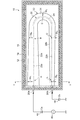
プラズマ発生装置10は、アンテナ20と、アンテナカバー30と、を備える。アンテナ20は、プラズマ室12の内部に設けられ、その中を流れるRF電流によって励起されるRF電界を表面からある距離の範囲で生じさせる。アンテナ20は、U字形状をしている。U字形状のアンテナ20の両端には、例えば、13.56MHzの高周波が入力される。
The
アンテナ20の一端は、第1容量Caを有する第1コンデンサ42を介して高周波電源40に接続される。アンテナ20の他端は、第2容量Cbを有する第2コンデンサ44を介して接地される。なお、第1コンデンサ42および第2コンデンサ44は、高周波電源40とのインピーダンス整合に用いられる整合器に対応し、インピーダンス整合に適切なコンデンサの容量Ca、Cbが選択される。なお、本実施の形態では、第1容量Caよりも第2容量Cbが大きい(Ca<Cbである)場合について説明する。
One end of the
アンテナカバー30は、アンテナ20の表面を被覆して、アンテナ20をプラズマPから保護する。アンテナカバー30は、U字形状のアンテナ20に対応して、U字の管形状を有する。アンテナカバー30は、石英(SiO2)や、アルミナ(Al2O3)などのセラミック材料により構成され、より好ましくは石英により構成される。
The
図2は、第1の実施の形態に係るプラズマ発生装置10を概略的に示す図であり、図1のX−X線断面を示す。図3は、第1の実施の形態に係るアンテナ20およびアンテナカバー30を示す外観斜視図である。なお、図1は、図2のY−Y線断面を示す。図示されるように、本実施の形態のアンテナカバー30は、U字形状のアンテナ20が延びる方向に沿って径方向の厚み(WA〜WE)が変化する構造を有する。ここで、径方向とは、アンテナ20が延びる方向に交差ないし直交する方向であり、アンテナ20の表面に交差ないし直交する方向である。
FIG. 2 is a diagram schematically showing the
アンテナ20は、第1直線部22aと、第2直線部22bと、円弧状に曲がった曲線部24とを有し、これらによりU字形状を構成する。アンテナ20は、棒状ないし中空状の導電性材料、例えば、銅(Cu)やアルミニウム(Al)で構成される。例えば、中空の銅パイプにU字状の曲げ加工を施したもので構成する。また、アンテナ20は、両端に第1端子20aと第2端子20bを有する。第1直線部22aに設けられる第1端子20aは、第1コンデンサ42を介して高周波電源40に接続される、第2直線部22bに設けられる第2端子20bは、第2コンデンサ44を介して接地される。
The
以下の説明において、アンテナ20の表面上の位置を説明するために、A地点、B地点
、C地点、D地点、E地点の表現を用いることがある。A地点は、第1直線部22aのうち第1端子20aに近い位置を示し、B地点は、第1直線部22aのうち曲線部24に近く、第1端子20aから離れた位置を示す。C地点は、曲線部24の中央部分の位置を示す。D地点は、第2直線部22bのうち曲線部24に近く、第2端子20bから離れた位置を示す。E地点は、第2直線部22bのうち第2端子20bに近い位置を示す。
In the following description, in order to describe the position on the surface of the
また、アンテナ20が延びる方向に直交する方向として、内方向、外方向、上方向、下方向の表現を用いることがある。内方向とは、U字形状のアンテナ20の内側に向かう方向であり、その反対方向が外方向である。上方向とは、アンテナ20のU字形状が作る面に交差する方向のうち引出開口18に向かう方向であり、その反対方向が下方向である。例えば、第1直線部22aが延びる方向を基準とした場合、図3に示すように、第1直線部22aから第2直線部22bに向かう方向が内方向、その反対が外方向である。また、第1直線部22aが延びる方向と内外方向の双方に直交する方向が上下方向であり、そのうち、引出開口18に向かう方向が上方向であり、その反対が下方向である。
In addition, expressions of the inner direction, the outer direction, the upper direction, and the lower direction may be used as directions orthogonal to the direction in which the
アンテナカバー30は、第1直線部22aを被覆する第1直線保護部32aと、第2直線部22bを被覆する第2直線保護部32bと、曲線部24を被覆する曲線保護部34とを有する。アンテナカバー30は、第1直線保護部32a、第2直線保護部32b、曲線保護部34が一体的に成型されたU字形状を有する。なお、それぞれの部材が分割され、これらの部材を組み合わせることによりU字形状のアンテナカバー30を構成してもよい。
The
第1直線保護部32aは、A地点およびB地点を含む第1直線部22aを被覆する中空部材である。第1直線保護部32aは、円錐の頂部から小円錐を取り除いた円錐台の形状を有しており、A地点を被覆する径方向の厚さWAが、B地点を被覆する径方向の厚さWBよりも大きい。したがって、第1直線保護部32aは、A地点からB地点に向かって径方向の厚さが徐々に小さくなる形状を有する。
The 1st straight
第2直線保護部32bは、D地点およびE地点を含む第2直線部22bを被覆する中空部材である。第2直線保護部32bは、円錐台の形状を有しており、D地点を被覆する径方向の厚さWDが、E地点を被覆する径方向の厚さWEよりも大きい。したがって、第2直線保護部32bは、D地点からE地点に向かって径方向の厚さが徐々に小さくなる形状を有する。
The second straight
曲線保護部34は、C地点を含む曲線部24を被覆し、曲線部24の形状に対応して円弧状(C字状)に曲がった中空部材である。曲線保護部34は、C地点における径方向の厚さWCが、B地点における径方向の厚さWBよりも小さく、D地点における径方向の厚さWDよりも大きくなるように形成される。また、曲線保護部34は、B地点からD地点に向かって径方向の厚さが徐々に小さくなる形状を有する。
Curve protective part 3 4 covers the
以上の形状の第1直線保護部32a、第2直線保護部32b、曲線保護部34を組み合わせることにより、アンテナカバー30は、アンテナ20が延びる方向に沿ってA地点からE地点に向けて径方向の厚さが徐々に小さくなる形状を有する。なお、径方向の厚さの変化の仕方は、線形的であってもよいし、非線形であってもよい。
By combining the first straight
なお、アンテナカバー30は、径方向の厚さがそれぞれの地点において等方的となるように形成される。ここで、径方向の厚さが等方的とは、アンテナ20が延びる方向に直交する方向のうち、異なる複数の方向に対する厚さがほぼ同じであることを意味し、例えば、内外方向それぞれの厚さと、上下方向それぞれの厚さがそれぞれ略等しいことを意味する。
The
つづいて、アンテナ20の表面上の位置に応じてアンテナカバー30の径方向の厚さを異ならせることとした理由について述べる。まず、比較例を用いてプラズマによるアンテナカバーの局所的な消耗について説明する。つづいて、本実施の形態におけるアンテナカバーの局所的消耗を抑制させる効果について説明する。
Next, the reason why the thickness in the radial direction of the
図4は、比較例に係るアンテナ20およびアンテナカバー80を模式的に示す図である。比較例に係るアンテナカバー80は、本実施の形態と異なり、径方向の厚さWが場所によらず一定となる形状を有する。比較例に係るアンテナ20は、本実施の形態と同様である。第1端子20aには、相対的に容量の小さい第1容量Caの第1コンデンサ42が接続され、第2端子20bには、相対的に容量の大きい第2容量Cbの第2コンデンサ44が接続される。
FIG. 4 is a diagram schematically illustrating the
プラズマ中におかれたアンテナカバー80の外表面には、プラズマ中の電子が帯電してシース(Sheath)が形成される。シースが形成されると、アンテナカバー80の外表面がプラズマに対して負の直流電位(DC電位)を有することとなり、プラズマ中の陽イオンが加速されながら引き寄せられてアンテナカバー80の外表面に衝突する。衝突する陽イオンのイオンエネルギーは、アンテナカバー80の外表面の電位に比例することから、外表面のうち電位の高い箇所にはイオンエネルギーの高い陽イオンが衝突し、アンテナカバー80の消耗が局所的に大きくなる。
On the outer surface of the
このとき、アンテナカバー80の外表面における電位は、アンテナ20の容量およびアンテナカバー80の容量により決められ、容量が小さいほど電位が大きくなる。U字形状のアンテナの場合、アンテナ容量はアンテナ20の両端に接続されるコンデンサの容量によって決められる。また、アンテナカバー80の容量は、アンテナカバー80の厚さや構成する材料の誘電率などにより決められる。比較例においては、アンテナカバー80の厚さが場所によらず一定であるため、アンテナ20の両端に接続されるコンデンサの容量Ca、Cbにより決まる。アンテナ20の両端に接続されるコンデンサ容量Ca、Cbは、非対称であるため、位置によってアンテナカバー80の外表面における電位が異なることとなる。
At this time, the potential on the outer surface of the
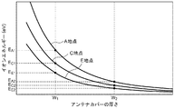
図5は、比較例に係るアンテナカバー80の厚さとアンテナカバー80の外表面におけるイオンエネルギーの関係を示すグラフである。比較例において、容量の小さい第1コンデンサ42が接続される第1端子20aに近いA地点では、アンテナカバー80の外表面でのイオンエネルギーが大きくなる。一方で、容量の大きい第2コンデンサ44が接続される第2端子20bに近いE地点では、アンテナカバー80の外表面でのイオンエネルギーが小さい。中間のC地点では、A地点とE地点の間のイオンエネルギーの値をとる。
FIG. 5 is a graph showing the relationship between the thickness of the
グラフにおいて、アンテナカバー80の厚さをW1とすると、A地点、C地点、E地点におけるイオンエネルギーは異なる値EA1、EC1、EE1となる。A地点におけるイオンエネルギーは他の地点と比べて大きいことから、カバーの消耗が激しく、他の場所よりも損傷しやすくなる。すると、アンテナカバー80の他の地点における消耗が小さい場合であっても、A地点における局所的な消耗によりアンテナカバー80が寿命を迎えてしまう。
In the graph, when the thickness of the
一方で、アンテナカバー80の厚さをW2にすると、A地点、C地点、E地点におけるイオンエネルギーを相対的に小さな値EA2、EC2、EE2とすることができるため、アンテナカバー80の消耗を低減させることができる。しかし、アンテナカバー80の厚さを全体的に厚くすると、アンテナ20からプラズマPまでの距離が大きくなり、それに従ってプラズマPが発生する位置でのRF電界も小さくなるため、プラズマの生成効率が低下してしまう。
On the other hand, when the thickness of the
なお、アンテナ20の両端に接続されるコンデンサ42、44の容量Ca、Cbが等しくなるようにすれば、アンテナ20の場所に応じたイオンエネルギーの差異を低減することができるかもしれない。しかしながら、アンテナ20に接続されるコンデンサ容量は、アンテナへの高周波供給手法によって決められてしまうことから、任意の値を取ることは難しい。一般的なインピーダンス整合器においては、アンテナ20の両端に接続されるコンデンサ容量は非対称となることが多い。
If the capacitors Ca and Cb of the
そこで、本実施の形態では、アンテナカバー30の厚みを場所によって変えることにより、アンテナカバー30の外表面における電位の空間依存性が低減されるようにする。図6は、実施の形態に係るアンテナカバー30の厚さとアンテナカバー30の外表面におけるイオンエネルギーの関係を示すグラフである。グラフに示すように、A地点、C地点、E地点の各地点におけるイオンエネルギーが同じ値Eとなるように、アンテナカバー30の厚さを各地点で変えて、それぞれWA、WC、WE(WA>WC>WE)とする。
Therefore, in the present embodiment, the spatial dependence of the potential on the outer surface of the
図2および図3を用いて上述した通り、アンテナ容量の小さいA地点の近くでは、アンテナカバー30の厚さを相対的に大きくし、アンテナ容量の大きいE地点に近づくほどアンテナカバー30の厚さを小さくする。これにより、アンテナカバー30に衝突する陽イオンのエネルギーを均一化させることができ、アンテナカバー30の局所的な消耗を抑制することができる。局所的な消耗を抑制させることで、アンテナカバー30の寿命を延ばすことができ、プラズマ発生装置10およびイオン注入装置100の信頼性を高めることができる。
As described above with reference to FIGS. 2 and 3, the thickness of the
また、本実施の形態では、アンテナカバー30の厚みを場所によって変えることにより、アンテナカバー30の容量を場所によって変えることができるとも言える。アンテナ20の容量が相対的に小さいA地点では、アンテナカバー30の厚さを大きくすることでアンテナ20の周囲における誘電率を高くし、アンテナカバー30の容量を大きくする。一方で、アンテナ20の容量が相対的に大きいE地点では、アンテナカバー30の厚さを小さくすることでアンテナ20の周囲における誘電率を低くし、アンテナカバー30の容量を小さくする。つまり、アンテナ20とアンテナカバー30の容量の双方を非対称とすることにより、アンテナ20とアンテナカバー30の容量の合計値の非対称性を低減させる。これにより、アンテナカバー30の外表面における電位の空間依存性を低減させて、アンテナカバー30の局所的な消耗を抑制することができる。
Moreover, in this Embodiment, it can be said that the capacity | capacitance of the
(第2の実施の形態)
図7は、第2の実施の形態に係るプラズマ発生装置10を概略的に示す図である。本実施の形態では、プラズマ室12の内部をプラズマが生成される第1区画12aと、アンテナ20が設けられる第2区画12bとに区画するアンテナカバー130を用いる点で、上述した第1の実施の形態と異なる。また、本実施の形態では、プラズマ室12の上半分の領域に相当する第1区画12aにプラズマPが生成されるよう構成される。以下、第1の実施の形態との相違点を中心に説明する。
(Second Embodiment)
FIG. 7 is a diagram schematically showing the
アンテナカバー130は、被覆部132と、区画部134と、を備える。区画部134は平板形状であり、プラズマ室12を構成する壁面のうち、引出開口18に対向する底面12cと対向して設けられる。これにより、区画部134は、プラズマ室12の内部を上下方向に二分し、主にプラズマPが生成される上半分の領域である第1区画12aと、プラズマが生成されない下半分の領域である第2区画12bとに仕切る。なお、平板形状の区画部134のうち、アンテナ20が配置される位置には溝部136が設けられる。溝部136には、上方向に突起する被覆部132が設けられる。
The
被覆部132は、U字形状のアンテナ20の表面を被覆して保護する。被覆部132は、円筒部材を軸方向に半分に切断したような形状を有し、アンテナ20の表面のうち主に上半分の領域を被覆するように設けられる。被覆部132は、区画部134から上方向に突出するように設けられており、内側にアンテナ20が収容される溝部136が設けられる。被覆部132を上方向に突出させることにより、第1区画12aの中央に近い位置にアンテナ20を配置することができる。
The covering
被覆部132は、アンテナ20の表面上の位置に応じて径方向の厚さが異なるように設けられる。第1の実施の形態と同様に、容量の小さい第1コンデンサ42の接続位置に近いA地点では、径方向の厚さを相対的に大きいWAとし、容量の大きい第2コンデンサ44の接続位置に近いE地点では、径方向の厚さが相対的に小さいWEとする。また、被覆部132は、アンテナ20が延びる方向にA地点からE地点に向かうにしたがって、径方向の厚さが徐々に小さくなるように設けられる。
The covering
第2の実施の形態においては、プラズマPが主にプラズマ室12の上半分の領域である第1区画12aに生成されるため、アンテナカバー130のうち、アンテナ20よりも上半分の領域である被覆部132がプラズマに曝される。アンテナカバー130の外表面における電位は、プラズマPが存在する方向に対する厚さによって決まる。したがって、アンテナカバー130の外表面におけるイオンエネルギーを均一化するためには、プラズマPに曝される箇所の厚さを適切に設定すればよいこととなる。
In the second embodiment, the plasma P is mainly generated in the
第2の実施の形態によれば、アンテナ20のアンテナ容量の非対称性に応じて被覆部132の厚さを変化させることで、プラズマPに曝される被覆部132の外表面においてイオンエネルギーを均一化させることができる。このため、アンテナカバー130がアンテナ20の全面を覆っていない場合であっても、上述の第1の実施の形態と同様の効果を得ることができる。
According to the second embodiment, the ion energy is made uniform on the outer surface of the covering
また、第2の実施の形態によれば、第1区画12aと第2区画12bを仕切る区画部134が設けられるため、アンテナ20が設けられる第2区画12bにプラズマが侵入することを防ぐことができる。これにより、アンテナ20の表面が溝部136の位置で露出していたとしても、プラズマPからアンテナ20を保護することができる。また、仮に第2区画12bにおいてプラズマが発生してアンテナ20がスパッタされ、金属粒子が発生する場合であっても、アンテナカバー130の仕切りにより第1区画12aのプラズマPが汚染されてしまうことを防ぐことができる。
In addition, according to the second embodiment, since the
また、第2の実施の形態によれば、第1の実施の形態よりも容易にアンテナカバー130をアンテナ20に取り付けることができる。第1の実施の形態では、アンテナカバー30がアンテナ20の表面の全体を被覆していることから、アンテナ20とアンテナカバー30を一体的に成型したり、分割された複数の部材を組み合わせてアンテナカバー30を形成する必要がある。一方、第2の実施の形態によれば、アンテナカバー130の溝部136にアンテナ20を嵌め込めばよいため、アンテナ20とアンテナカバー130を別々に成型することが容易となり、また、組み立てもしやすい。
Further, according to the second embodiment, the
(第3の実施の形態)
図8は、第3の実施の形態に係るプラズマ発生装置10を概略的に示す図であり、図9は、第3の実施の形態に係るアンテナカバー180を示す外観斜視図である。本実施の形態では、アンテナ20の上半分を被覆する被覆部182の断面形状が矩形状であり、被覆部182の外表面が平坦な上面182a、外側面182b、内側面182cにより構成される点で、上述した第2の実施の形態と異なる。本実施の形態では、第1区画12aのうち、主にアンテナ20の内側の領域にプラズマPが生成されるよう構成される。以下、第2の実施の形態との相違点を中心に説明する。
(Third embodiment)
FIG. 8 is a diagram schematically showing a
アンテナカバー180は、被覆部182と、区画部184と、を備える。区画部184は、上述した第2の実施の形態に係る区画部134と同様の構成を有する。一方、被覆部182は、アンテナ20が延びる方向の断面が略矩形状であり、アンテナ20が延びる方向に長い角柱部材の一面にアンテナ20を収容するための溝部186を形成した形状を有する。
The
被覆部182は、第1区画12aに接する面として、上面182aと、外側面182bと、内側面182cとを有する。上面182aは、アンテナ20から上方向に離れて設けられる面である。同様に、外側面182bは、アンテナ20から外方向に離れて設けられる面であり、内側面182cは、アンテナ20から内方向に離れて設けられる面である。
The covering
被覆部182の径方向の厚さは、その方向によって厚さが異なる。アンテナ20から上面182aまでの厚さは、アンテナ20が延びる方向に沿って変化させず、一定の値Wupとなるように設けられる。同様に、アンテナ20から外側面182bまでの厚さは、アンテナ20が延びる方向に沿って変化させず、一定の値Woutとなるように設けられる。上面182aおよび外側面182bは、プラズマPに曝されにくい位置にあるため、その厚さを変化させたとしてもアンテナカバー180の局所的な消耗の低減には寄与しにくいからである。
The thickness in the radial direction of the covering
一方、アンテナ20から内側面182cまでの厚さは、上面182aや外側面182bとは相違して、アンテナ20が延びる方向の位置によって異なる厚さとしている。例えば、容量の小さい第1コンデンサ42の接続位置に近いA地点では、径方向の厚さを相対的に大きいWAinとし、容量の大きい第2コンデンサ44の接続位置に近いE地点では、径方向の厚さが相対的に小さいWEinとする。内側面182cは、アンテナ20の内側の領域に生成されるプラズマPに曝される位置にあるため、その厚さを変化させることで、アンテナカバー180の局所的な消耗の低減に寄与するからである。
On the other hand, the thickness from the
図10は、プラズマ発生装置10を概略的に示す図であり、図8のX−X線断面を示す。被覆部182は、第1直線部22aを保護する第1直線保護部192aと、第2直線部22bを保護する第2直線保護部192bと、曲線部24を保護する曲線保護部194とを有する。
FIG. 10 is a diagram schematically showing the
図示されるように、被覆部182の径方向の厚さのうち、外方向の厚さは、第1直線保護部192aおよび第2直線保護部192bにおいて一定のWoutとなっている。言いかえれば、A地点、B地点、D地点、E地点においては、外方向の厚さを一定のWoutとしている。一方、曲線保護部194においては、曲線部24の形状によらずに外方向の厚さを任意に設定することで、曲線保護部194における外側面194bが平坦面となるようにしている。外方向の厚さをこのように設定することで、アンテナ20が延びる方向に沿って厚さを変化させる場合よりも、アンテナカバー180の成型が容易となる。
As shown in the drawing, out of the radial thicknesses of the covering
また、被覆部182の径方向の厚さのうち、内方向の厚さは、第1直線保護部192aにおいて一定のWAinとし、第2直線保護部192bにおいて一定のWBinとしている。言いかえれば、A地点およびB地点では、外方向の厚さを共通のWAinとし、D地点およびE地点では、外方向の厚さを共通のWEinとしている。一方、曲線保護部194における内方向の厚さは、B地点からD地点に向けて徐々に小さくなるようにし、C地点における内方向の厚さをWCinとしてている。したがって、B地点、C地点、D地点の内方向の厚さは、WAin>WCin>WEinの関係となる。
Also, of the radial thickness of the covering
第3の実施の形態では、被覆部182の径方向の厚さについて、外方向および上方向についてはアンテナ20の位置によらず任意の値を設定することにより、アンテナカバー180の加工容易性を高めている。一方で、主にプラズマに曝されることとなる内側面182cに対する厚さ、つまり、プラズマに向かう内方向の厚さについては、アンテナ20の位置に応じて厚さを変化させることとする。これにより、プラズマにより消耗しやすい内側面182cにおけるイオンエネルギーを均一化させて、アンテナカバー180の局所的な消耗を低減させることができる。
In the third embodiment, the processability of the
また、第3の実施の形態では、第1直線保護部192aおよび第2直線保護部192bにおいて内方向の厚さを一定値とすることで、内側面182cの加工容易性を高めている。この場合、内側面182cにおけるイオンエネルギーを空間依存性を低減させる効果は下がるものの、第1直線保護部192aと第2直線保護部192bとでは厚さが異なるため、第1直線保護部192aにおける消耗度と第2直線保護部192bにおける消耗度の差を低減させることができる。これにより、加工容易性を持たせつつ、局所的な消耗を低減させることのできるアンテナカバー180とすることができる。
Further, in the third embodiment, the processability of the
(第4の実施の形態)
図11は、第4の実施の形態に係るプラズマ発生装置210を概略的に示す図である。本実施の形態は、アンテナ220がU字形状ではなく直線形状である点で、上述の実施の形態と相違する。また、アンテナカバー230も、アンテナ220に対応して直線形状を有する。以下、上述の実施の形態との相違点を中心に説明する。
(Fourth embodiment)
FIG. 11 is a diagram schematically showing a
プラズマ発生装置210は、プラズマ室12と、磁石装置14と、絶縁部材16と、引出開口18と、アンテナ220と、アンテナカバー230と、を備える。プラズマ室12の内部には、直線形状のアンテナ220と、アンテナ220の表面を保護するアンテナカバー230が設けられる。
The
アンテナ220は、両端に第1端子220aと、第2端子220bと、を有する。第1端子220aは、第1容量Caの第1コンデンサ42を介して高周波電源40に接続され、第2端子220bは、第2容量Cbの第2コンデンサ44を介して接地される。コンデンサ42、44の容量は、第1容量Caよりも第2容量Cbが大きい(Ca<Cbである)。
The
アンテナカバー230は、直線状のアンテナ220を被覆する中空部材である。アンテナカバー230は、円錐台の形状を有しており、第1端子220aの近傍を被覆する第1端部230aにおける径方向の厚さWAが、第2端子220bの近傍を被覆する第2端部230bにおける径方向の厚さWBよりも大きい。したがって、アンテナカバー230は、第1端部230aから第2端部230bに向かって径方向の厚さが徐々に小さくなる形状を有する。
The
第4の実施の形態においても、アンテナ容量の小さい第1端子220aの近くでは、アンテナカバー230の厚さを相対的に大きくし、アンテナ容量の大きい第2端子220bに近づくほどアンテナカバー230の厚さを小さくする。これにより、アンテナカバー230に衝突する陽イオンのエネルギーを均一化させることができ、アンテナカバー230の局所的な消耗を抑制することができる。局所的な消耗を抑制させることで、アンテナカバー230の寿命を延ばすことができる。
Also in the fourth embodiment, the thickness of the
以上、本発明を実施例にもとづいて説明した。本発明は上記実施形態に限定されず、種々の設計変更が可能であり、様々な変形例が可能であること、またそうした変形例も本発明の範囲にあることは、当業者に理解されるところである。 In the above, this invention was demonstrated based on the Example. It will be understood by those skilled in the art that the present invention is not limited to the above-described embodiment, and various design changes are possible, various modifications are possible, and such modifications are within the scope of the present invention. By the way.
上述の実施の形態では、アンテナの両端のうち、相対的に小さい容量Caの第1コンデンサが接続される第1端子側に高周波電源を接続し、相対的に大きい容量Cbの第2コンデンサが接続される第2端子側を接地する場合について説明した。変形例においては、容量の小さい第1端子側を接地し、容量Cbが大きい第2端子側に高周波電源を接続してもよい。この場合、アンテナ容量の小さい第1端子側のアンテナカバーの厚さを大きくし、アンテナ容量の大きい第2端子側のアンテナカバーの厚さを小さくすればよい。 In the above-described embodiment, the high-frequency power source is connected to the first terminal side to which the first capacitor having the relatively small capacitance Ca is connected, and the second capacitor having the relatively large capacitance Cb is connected. The case where the second terminal side to be grounded is described. In a modified example, the first terminal having a small capacity may be grounded, and the high frequency power source may be connected to the second terminal having a large capacity Cb. In this case, the thickness of the antenna cover on the first terminal side having a small antenna capacity may be increased, and the thickness of the antenna cover on the second terminal side having a large antenna capacity may be reduced.
上述の実施の形態では、U字形状のアンテナの表面の全体や、上半分の全体を覆うアンテナカバーについて説明した。変形例においては、アンテナ経路の一部分に相当する表面のみを覆うアンテナカバーとしてもよい。例えば、U字形状の曲線部にはアンテナカバーを設けず、直線部のみにアンテナカバーを設けることとしてもよい。また、プラズマが生成される位置の近傍にのみアンテナカバーを設けることとしてもよい。 In the above-described embodiment, the antenna cover that covers the entire surface of the U-shaped antenna and the entire upper half has been described. In a modification, it is good also as an antenna cover which covers only the surface equivalent to a part of antenna path. For example, the antenna cover may be provided only on the straight line portion without providing the antenna cover on the U-shaped curved portion. Moreover, it is good also as providing an antenna cover only in the vicinity of the position where plasma is generated.
上述の実施の形態では、U字形状のアンテナが延びる経路に沿って、径方向の厚さが徐々に小さくなる形状のアンテナカバーについて説明した。変形例においては、アンテナ経路のある区間において、径方向におけるアンテナカバーの厚さを一定にすることとしてもよい。例えば、第1直線部と曲線部の厚さを一定にし、第2直線部の厚さをそれよりも小さい一定値としてもよい。第1直線部の厚さを一定にし、曲線部と第2直線部の厚さをそれよりも小さい一定値としてもよい。このとき、第1直線部と第2直線部とで厚さに差をもうけることで、アンテナカバーの外表面におけるイオンエネルギーの相対差を低減させることができる。 In the above-described embodiment, the antenna cover having a shape in which the radial thickness gradually decreases along the path along which the U-shaped antenna extends has been described. In a modification, the thickness of the antenna cover in the radial direction may be constant in a certain section of the antenna path. For example, the thickness of the first straight line portion and the curved line portion may be constant, and the thickness of the second straight line portion may be a constant value smaller than that. The thickness of the first linear portion may be constant, and the thickness of the curved portion and the second linear portion may be a constant value smaller than that. At this time, a relative difference in ion energy on the outer surface of the antenna cover can be reduced by making a difference in thickness between the first straight portion and the second straight portion.
上述の実施の形態では、径方向の厚さのうち内方向の厚さをアンテナ経路に沿って変化させ、それ以外の厚さについては任意の厚さとするアンテナカバーについて説明した。変形例においては、径方向におけるアンテナカバーの厚さのうち、少なくとも一方向についてはアンテナ経路に沿って変化させる一方で、別の方向についてはアンテナ経路によらず一定値または任意の値とすることとしてもよい。この場合、プラズマに向かう方向におけるアンテナカバーの厚さをアンテナ経路に沿って変化させることで、プラズマの影響を受けやすい箇所におけるイオンエネルギーの相対差を低減させることができる。例えば、プラズマがアンテナの外側の領域において主に生成される場合においては、内方向の厚さは任意の値とし、上下方向や、外方向におけるアンテナカバーの厚さをアンテナ経路に沿って変化させることとしてもよい。 In the above-described embodiment, the antenna cover has been described in which the inner thickness of the radial thickness is changed along the antenna path, and the other thicknesses are arbitrary. In the modification, of the thickness of the antenna cover in the radial direction, at least one direction is changed along the antenna path, while the other direction is a constant value or an arbitrary value regardless of the antenna path. It is good. In this case, by changing the thickness of the antenna cover in the direction toward the plasma along the antenna path, it is possible to reduce the relative difference in ion energy at a location that is susceptible to plasma. For example, when plasma is mainly generated in the region outside the antenna, the thickness in the inner direction is an arbitrary value, and the thickness of the antenna cover in the vertical direction or the outer direction is changed along the antenna path. It is good as well.
10…プラズマ発生装置、12…プラズマ室、20…アンテナ、20a…第1端子、20b…第2端子、22a…第1直線部、22b…第2直線部、24…曲線部、30…アンテナカバー、32a…第1直線保護部、32b…第2直線保護部、34…曲線保護部、40…高周波電源、130…アンテナカバー、132…被覆部、134…区画部、180…アンテナカバー、182…被覆部、184…区画部、192a…第1直線保護部、192b…第2直線保護部、194…曲線保護部、P…プラズマ。
DESCRIPTION OF
Claims (9)
前記アンテナは、整合器を介して高周波電源に接続される第1端子および第2端子を備え、前記第1端子を有する第1直線部と、前記第2端子を有する第2直線部と、前記第1直線部と前記第2直線部を接続する曲線部と、により構成されるU字形状を有しており、
前記アンテナカバーは、前記第1直線部の表面を保護する第1直線保護部と、前記第2直線部の表面を保護する第2直線保護部と、前記曲線部の表面を保護する曲線保護部と、を備え、
前記アンテナカバーは、当該アンテナカバーの外表面における電位の空間依存性が低減されるように、前記アンテナの表面に直交する方向のうち少なくとも一方向におけるアンテナカバーの厚さが、当該表面上の位置に応じて異なり、
前記第1直線保護部における前記少なくとも一方向の厚さは、前記第2直線保護部における前記少なくとも一方向の厚さよりも大きいことを特徴とするアンテナカバー。 An antenna cover that is provided inside the plasma chamber and protects the surface of the antenna that radiates high frequency into the plasma chamber,
The antenna includes a first terminal and a second terminal connected to a high-frequency power source through a matching unit, a first straight part having the first terminal, a second straight part having the second terminal, It has a U-shape composed of a first straight part and a curved part connecting the second straight part,
The antenna cover includes a first straight line protection part that protects the surface of the first straight line part, a second straight line protection part that protects the surface of the second straight line part, and a curved line protection part that protects the surface of the curved part. And comprising
In the antenna cover, the thickness of the antenna cover in at least one of the directions orthogonal to the surface of the antenna is a position on the surface so that the spatial dependence of the potential on the outer surface of the antenna cover is reduced. different depending on the Ri,
The antenna cover according to claim 1, wherein a thickness of the first linear protective part in the at least one direction is larger than a thickness of the second linear protective part in the at least one direction .
前記第1コンデンサの第1容量は、前記第2コンデンサの第2容量よりも小さいことを特徴とする請求項1または2に記載のアンテナカバー。The antenna cover according to claim 1 or 2, wherein the first capacitor of the first capacitor is smaller than the second capacitor of the second capacitor.
前記プラズマ室の内部に磁場を印加する磁石と、
前記プラズマ室の内部に設けられ、当該プラズマ室内に高周波を放射するアンテナと、
前記アンテナの表面を保護するアンテナカバーと、
を備え、
前記アンテナは、整合器を介して高周波電源に接続される第1端子および第2端子を備え、前記第1端子を有する第1直線部と、前記第2端子を有する第2直線部と、前記第1直線部と前記第2直線部を接続する曲線部と、により構成されるU字形状を有しており、
前記アンテナカバーは、前記第1直線部の表面を保護する第1直線保護部と、前記第2直線部の表面を保護する第2直線保護部と、前記曲線部の表面を保護する曲線保護部と、を備え、
前記アンテナカバーは、当該アンテナカバーの外表面における電位の空間依存性が低減されるように、前記アンテナの表面に直交する方向のうち少なくとも一方向におけるアンテナカバーの厚さが、当該表面上の位置に応じて異なり、
前記第1直線保護部における前記少なくとも一方向の厚さは、前記第2直線保護部における前記少なくとも一方向の厚さよりも大きいことを特徴とするプラズマ発生装置。 A plasma chamber;
A magnet for applying a magnetic field to the inside of the plasma chamber;
An antenna that is provided inside the plasma chamber and radiates high frequency into the plasma chamber;
An antenna cover for protecting the surface of the antenna;
With
The antenna includes a first terminal and a second terminal connected to a high-frequency power source through a matching unit, a first straight part having the first terminal, a second straight part having the second terminal, It has a U-shape composed of a first straight part and a curved part connecting the second straight part,
The antenna cover includes a first straight line protection part that protects the surface of the first straight line part, a second straight line protection part that protects the surface of the second straight line part, and a curved line protection part that protects the surface of the curved part. And comprising
In the antenna cover, the thickness of the antenna cover in at least one of the directions orthogonal to the surface of the antenna is a position on the surface so that the spatial dependence of the potential on the outer surface of the antenna cover is reduced. different depending on the Ri,
The plasma generator according to claim 1, wherein the thickness in the at least one direction of the first linear protection part is larger than the thickness in the at least one direction of the second linear protection part .
Priority Applications (5)
| Application Number | Priority Date | Filing Date | Title |
|---|---|---|---|
| JP2013256014A JP6147177B2 (en) | 2013-12-11 | 2013-12-11 | Antenna cover and plasma generator using the same |
| TW103141194A TWI659567B (en) | 2013-12-11 | 2014-11-27 | Radome cover and plasma generating device using the same |
| CN201410738797.5A CN104716424B (en) | 2013-12-11 | 2014-12-05 | Antenna cover and plasma generating device using same |
| KR1020140174770A KR102226099B1 (en) | 2013-12-11 | 2014-12-08 | Antenna cover and device for generating plasma using the same |
| US14/566,133 US9502759B2 (en) | 2013-12-11 | 2014-12-10 | Antenna cover and plasma generating device using same |
Applications Claiming Priority (1)
| Application Number | Priority Date | Filing Date | Title |
|---|---|---|---|
| JP2013256014A JP6147177B2 (en) | 2013-12-11 | 2013-12-11 | Antenna cover and plasma generator using the same |
Publications (3)
| Publication Number | Publication Date |
|---|---|
| JP2015115172A JP2015115172A (en) | 2015-06-22 |
| JP2015115172A5 JP2015115172A5 (en) | 2016-04-28 |
| JP6147177B2 true JP6147177B2 (en) | 2017-06-14 |
Family
ID=53272106
Family Applications (1)
| Application Number | Title | Priority Date | Filing Date |
|---|---|---|---|
| JP2013256014A Active JP6147177B2 (en) | 2013-12-11 | 2013-12-11 | Antenna cover and plasma generator using the same |
Country Status (5)
| Country | Link |
|---|---|
| US (1) | US9502759B2 (en) |
| JP (1) | JP6147177B2 (en) |
| KR (1) | KR102226099B1 (en) |
| CN (1) | CN104716424B (en) |
| TW (1) | TWI659567B (en) |
Families Citing this family (3)
| Publication number | Priority date | Publication date | Assignee | Title |
|---|---|---|---|---|
| CN109300758A (en) * | 2018-09-27 | 2019-02-01 | 德淮半导体有限公司 | Ion Implantation Equipment and ion source generating device |
| CN113972475B (en) * | 2020-07-24 | 2024-03-08 | 启碁科技股份有限公司 | Antenna structure |
| US20230083497A1 (en) * | 2021-09-15 | 2023-03-16 | Applied Materials, Inc. | Uniform plasma linear ion source |
Family Cites Families (16)
| Publication number | Priority date | Publication date | Assignee | Title |
|---|---|---|---|---|
| US5824158A (en) | 1993-06-30 | 1998-10-20 | Kabushiki Kaisha Kobe Seiko Sho | Chemical vapor deposition using inductively coupled plasma and system therefor |
| JPH0718433A (en) | 1993-06-30 | 1995-01-20 | Kobe Steel Ltd | Icp sputtering device |
| JP4122467B2 (en) | 1998-02-17 | 2008-07-23 | 株式会社東芝 | High frequency discharge device and high frequency processing device |
| JPH11317299A (en) * | 1998-02-17 | 1999-11-16 | Toshiba Corp | High frequency discharge method, its device, and high frequency processing device |
| JP4089022B2 (en) | 1998-07-22 | 2008-05-21 | 日新イオン機器株式会社 | Self-electron emission type ECR ion plasma source |
| JP2001203099A (en) * | 2000-01-20 | 2001-07-27 | Yac Co Ltd | Plasma generator and plasma processing apparatus |
| KR100523851B1 (en) * | 2003-05-07 | 2005-10-27 | 학교법인 성균관대학 | Inductively Coupled Plasma Processing Appratus having internal linear antenna for large area processing |
| JP5162108B2 (en) * | 2005-10-28 | 2013-03-13 | 日新電機株式会社 | Plasma generating method and apparatus, and plasma processing apparatus |
| JP4001185B1 (en) | 2007-03-06 | 2007-10-31 | 日新イオン機器株式会社 | Plasma generator |
| JP5329796B2 (en) * | 2007-11-14 | 2013-10-30 | 株式会社イー・エム・ディー | Plasma processing equipment |
| KR20090079696A (en) * | 2008-01-18 | 2009-07-22 | 삼성전자주식회사 | Plasma treatment apparatus having linear antenna |
| JP4992885B2 (en) | 2008-11-21 | 2012-08-08 | 日新イオン機器株式会社 | Plasma generator |
| TW201105183A (en) * | 2009-07-21 | 2011-02-01 | Delta Electronics Inc | Plasma generating apparatus |
| CN101990352A (en) * | 2009-08-07 | 2011-03-23 | 台达电子工业股份有限公司 | Plasma generating device |
| US20140210337A1 (en) * | 2011-08-30 | 2014-07-31 | Emd Corporation | Antenna for plasma processing device, and plasma processing device using the same |
| JP2013089477A (en) * | 2011-10-19 | 2013-05-13 | Nissin Electric Co Ltd | Plasma generator |
-
2013
- 2013-12-11 JP JP2013256014A patent/JP6147177B2/en active Active
-
2014
- 2014-11-27 TW TW103141194A patent/TWI659567B/en active
- 2014-12-05 CN CN201410738797.5A patent/CN104716424B/en active Active
- 2014-12-08 KR KR1020140174770A patent/KR102226099B1/en active IP Right Grant
- 2014-12-10 US US14/566,133 patent/US9502759B2/en active Active
Also Published As
| Publication number | Publication date |
|---|---|
| CN104716424B (en) | 2020-08-21 |
| TW201524006A (en) | 2015-06-16 |
| US9502759B2 (en) | 2016-11-22 |
| KR20150068307A (en) | 2015-06-19 |
| TWI659567B (en) | 2019-05-11 |
| JP2015115172A (en) | 2015-06-22 |
| CN104716424A (en) | 2015-06-17 |
| KR102226099B1 (en) | 2021-03-09 |
| US20150162657A1 (en) | 2015-06-11 |
Similar Documents
| Publication | Publication Date | Title |
|---|---|---|
| KR101456810B1 (en) | Plasma processing apparatus | |
| KR20080077670A (en) | Technique for providing an inductively coupled radio frequency plasma flood gun | |
| EP3648553B1 (en) | Plasma treatment device | |
| US20070084405A1 (en) | Adaptive plasma source for generating uniform plasma | |
| US20090189083A1 (en) | Ion-beam source | |
| JPWO2007029777A1 (en) | Ion source and plasma processing apparatus | |
| JP6227408B2 (en) | Vacuum variable capacitor | |
| US20130081761A1 (en) | Radical passing device and substrate processing apparatus | |
| WO2013030953A1 (en) | Antenna for plasma processing apparatus, and plasma processing apparatus using antenna | |
| JP6147177B2 (en) | Antenna cover and plasma generator using the same | |
| WO2011139587A1 (en) | Small form factor plasma source for high density wide ribbon ion beam generation | |
| JP5325623B2 (en) | Electron source | |
| US9721760B2 (en) | Electron beam plasma source with reduced metal contamination | |
| EP2562786B1 (en) | Ion pump system | |
| KR102417574B1 (en) | Ionizing Vacuum Gauges and Cartridges | |
| US20110163674A1 (en) | Mitigation of plasma-inductor termination | |
| KR102584240B1 (en) | Plasma generator using ferrite shield for focused inductive coupled plasma | |
| WO1999066531A1 (en) | Plasma processing apparatus | |
| US20240128052A1 (en) | Inductively coupled plasma apparatus with novel faraday shield | |
| JP7429154B2 (en) | Microwave ion source and particle acceleration system equipped with it | |
| WO2024081735A1 (en) | Inductively coupled plasma apparatus with novel faraday shield | |
| US9214318B1 (en) | Electromagnetic electron reflector | |
| JP2015079589A (en) | Microwave ion source | |
| JP2017123265A (en) | Ion source and insulating mechanism | |
| JP2017134934A (en) | Ion source |
Legal Events
| Date | Code | Title | Description |
|---|---|---|---|
| A625 | Written request for application examination (by other person) |
Free format text: JAPANESE INTERMEDIATE CODE: A625 Effective date: 20160215 |
|
| A521 | Written amendment |
Free format text: JAPANESE INTERMEDIATE CODE: A523 Effective date: 20160314 |
|
| A131 | Notification of reasons for refusal |
Free format text: JAPANESE INTERMEDIATE CODE: A131 Effective date: 20161101 |
|
| A521 | Written amendment |
Free format text: JAPANESE INTERMEDIATE CODE: A523 Effective date: 20161214 |
|
| TRDD | Decision of grant or rejection written | ||
| A01 | Written decision to grant a patent or to grant a registration (utility model) |
Free format text: JAPANESE INTERMEDIATE CODE: A01 Effective date: 20170516 |
|
| A61 | First payment of annual fees (during grant procedure) |
Free format text: JAPANESE INTERMEDIATE CODE: A61 Effective date: 20170516 |
|
| R150 | Certificate of patent or registration of utility model |
Ref document number: 6147177 Country of ref document: JP Free format text: JAPANESE INTERMEDIATE CODE: R150 |