JP6135403B2 - Information processing system and information processing system failure processing method - Google Patents
Information processing system and information processing system failure processing method Download PDFInfo
- Publication number
- JP6135403B2 JP6135403B2 JP2013175250A JP2013175250A JP6135403B2 JP 6135403 B2 JP6135403 B2 JP 6135403B2 JP 2013175250 A JP2013175250 A JP 2013175250A JP 2013175250 A JP2013175250 A JP 2013175250A JP 6135403 B2 JP6135403 B2 JP 6135403B2
- Authority
- JP
- Japan
- Prior art keywords
- node
- interrupt factor
- failure
- interrupt
- fnl
- Prior art date
- Legal status (The legal status is an assumption and is not a legal conclusion. Google has not performed a legal analysis and makes no representation as to the accuracy of the status listed.)
- Active
Links
Images


Classifications
-
- G—PHYSICS
- G06—COMPUTING; CALCULATING OR COUNTING
- G06F—ELECTRIC DIGITAL DATA PROCESSING
- G06F13/00—Interconnection of, or transfer of information or other signals between, memories, input/output devices or central processing units
- G06F13/14—Handling requests for interconnection or transfer
- G06F13/20—Handling requests for interconnection or transfer for access to input/output bus
- G06F13/24—Handling requests for interconnection or transfer for access to input/output bus using interrupt
-
- G—PHYSICS
- G06—COMPUTING; CALCULATING OR COUNTING
- G06F—ELECTRIC DIGITAL DATA PROCESSING
- G06F11/00—Error detection; Error correction; Monitoring
- G06F11/07—Responding to the occurrence of a fault, e.g. fault tolerance
- G06F11/0703—Error or fault processing not based on redundancy, i.e. by taking additional measures to deal with the error or fault not making use of redundancy in operation, in hardware, or in data representation
- G06F11/0706—Error or fault processing not based on redundancy, i.e. by taking additional measures to deal with the error or fault not making use of redundancy in operation, in hardware, or in data representation the processing taking place on a specific hardware platform or in a specific software environment
- G06F11/0709—Error or fault processing not based on redundancy, i.e. by taking additional measures to deal with the error or fault not making use of redundancy in operation, in hardware, or in data representation the processing taking place on a specific hardware platform or in a specific software environment in a distributed system consisting of a plurality of standalone computer nodes, e.g. clusters, client-server systems
-
- G—PHYSICS
- G06—COMPUTING; CALCULATING OR COUNTING
- G06F—ELECTRIC DIGITAL DATA PROCESSING
- G06F11/00—Error detection; Error correction; Monitoring
- G06F11/07—Responding to the occurrence of a fault, e.g. fault tolerance
- G06F11/16—Error detection or correction of the data by redundancy in hardware
- G06F11/20—Error detection or correction of the data by redundancy in hardware using active fault-masking, e.g. by switching out faulty elements or by switching in spare elements
- G06F11/202—Error detection or correction of the data by redundancy in hardware using active fault-masking, e.g. by switching out faulty elements or by switching in spare elements where processing functionality is redundant
- G06F11/2023—Failover techniques
- G06F11/2028—Failover techniques eliminating a faulty processor or activating a spare
-
- G—PHYSICS
- G06—COMPUTING; CALCULATING OR COUNTING
- G06F—ELECTRIC DIGITAL DATA PROCESSING
- G06F11/00—Error detection; Error correction; Monitoring
- G06F11/07—Responding to the occurrence of a fault, e.g. fault tolerance
- G06F11/16—Error detection or correction of the data by redundancy in hardware
- G06F11/20—Error detection or correction of the data by redundancy in hardware using active fault-masking, e.g. by switching out faulty elements or by switching in spare elements
- G06F11/202—Error detection or correction of the data by redundancy in hardware using active fault-masking, e.g. by switching out faulty elements or by switching in spare elements where processing functionality is redundant
- G06F11/2035—Error detection or correction of the data by redundancy in hardware using active fault-masking, e.g. by switching out faulty elements or by switching in spare elements where processing functionality is redundant without idle spare hardware
-
- G—PHYSICS
- G06—COMPUTING; CALCULATING OR COUNTING
- G06F—ELECTRIC DIGITAL DATA PROCESSING
- G06F11/00—Error detection; Error correction; Monitoring
- G06F11/07—Responding to the occurrence of a fault, e.g. fault tolerance
- G06F11/16—Error detection or correction of the data by redundancy in hardware
- G06F11/20—Error detection or correction of the data by redundancy in hardware using active fault-masking, e.g. by switching out faulty elements or by switching in spare elements
- G06F11/202—Error detection or correction of the data by redundancy in hardware using active fault-masking, e.g. by switching out faulty elements or by switching in spare elements where processing functionality is redundant
- G06F11/2043—Error detection or correction of the data by redundancy in hardware using active fault-masking, e.g. by switching out faulty elements or by switching in spare elements where processing functionality is redundant where the redundant components share a common memory address space
Description
本発明は、情報処理システム、情報処理システムの障害処理方法に関する。 The present invention relates to an information processing system and a failure processing method for the information processing system.
複数のノードを有する情報処理システムは、例えば、ビルディングブロック(BB:Building Block)構造を有する。例えば、複数のノードでメモリを共有する情報処理システムは、ノード間で、クロスバーを介してメモリを共有する。情報処理システムで動作するアプリケーションは、共有されたメモリを使用することによって、システムの処理性能の向上を図る。一方、それぞれのノードで動作するOS(Operation system、以下、OSと称する)やハイパーバイザ(hypervisor)は、各ノードのローカルメモリ上で動作する。OSやハイパーバイザがローカルメモリ上で動作することにより、各ノードの独立性が高まり、システムの可用性が向上する。 An information processing system having a plurality of nodes has, for example, a building block (BB) structure. For example, an information processing system that shares memory among a plurality of nodes shares the memory between the nodes via a crossbar. Applications that operate in the information processing system use a shared memory to improve the processing performance of the system. On the other hand, an OS (Operation System, hereinafter referred to as OS) and a hypervisor operating on each node operate on the local memory of each node. By operating the OS and the hypervisor on the local memory, the independence of each node is increased and the availability of the system is improved.
このような情報処理システムにおいて、一部のノードのハードウェアに障害が発生した場合、障害が発生した障害ノードを検出すると共に、障害ノードをシステムから切り離した状態で、運用を再開することが求められる。ハードウェアの障害の検出は、例えば、特許文献1に記載される。
In such an information processing system, when a failure occurs in the hardware of some nodes, it is necessary to detect the failed node and restart the operation with the failed node disconnected from the system. It is done. The detection of a hardware failure is described in
情報処理システムは、障害ノードの特定やシステムからの切り離しの要否を、障害の事象を有するログ情報に基づいて、順次、解析する。したがって、情報処理システムのノード数や、障害の事象の種類の増加に伴って、障害ノードの特定やシステムからの切り離しの要否に係る解析時間も増加する。また、ログ情報のデータ量が膨大であることにより、ログ情報の収集にも時間を要する。 The information processing system sequentially analyzes whether or not it is necessary to identify a faulty node or disconnect from the system based on log information having a fault event. Therefore, as the number of nodes in the information processing system and the types of failure events increase, the analysis time related to the necessity of identifying the failure node and disconnecting from the system also increases. Further, since the amount of log information is enormous, it also takes time to collect log information.
1つの側面は、本発明は、障害発生時に障害ノードによる他ノードの影響を早急に低減する情報処理システム、情報処理システムの障害処理方法を提供することを目的とする。 An object of one aspect of the present invention is to provide an information processing system and a failure processing method for an information processing system that quickly reduce the influence of another node due to the failed node when a failure occurs.
第1の側面は、複数のノード間でメモリを共有する情報処理システムにおいて、前記ノードの各々は、複数の機能回路と前記機能回路を制御する制御装置と、前記複数の機能回路から発生する割り込み要因を格納するレジスタとを有し、前記複数のノードのうちの1のノードの前記制御装置は、他の前記ノードの割り込み要因の発生に応じて前記レジスタの前記割り込み要因を受信し、前記割り込み要因のうち、障害として検出すべき割り込み要因を抽出して、抽出結果に応じて障害ノードを特定し、前記障害ノードの前記メモリへのアクセスを抑止後、前記他のノードから受信したログ情報に基づいて前記障害ノードの切り離し制御を行う。 In a first aspect of the information processing system in which a memory is shared among a plurality of nodes, each of the nodes includes a plurality of functional circuits, a control device that controls the functional circuits, and an interrupt generated from the plurality of functional circuits. A register for storing a factor, and the control device of one of the plurality of nodes receives the interrupt factor of the register in response to occurrence of an interrupt factor of the other node, and Among the factors, an interrupt factor to be detected as a failure is extracted, a failed node is identified according to the extraction result, and access to the memory of the failed node is suppressed, and then the log information received from the other nodes Based on this, the failure node is controlled to be separated.
第1の側面によれば、情報処理システムは、割り込み要因のうち、障害として検出すべき割り込み要因を抽出して、抽出結果に応じて障害ノードを特定し、障害ノードのメモリへのアクセスを抑止することで、障害発生時に障害ノードによる他ノードの影響を早急に低減する。 According to the first aspect, the information processing system extracts an interrupt factor that should be detected as a failure from among the interrupt factors, identifies the failed node according to the extraction result, and suppresses access to the memory of the failed node By doing so, the influence of other nodes due to the failed node is quickly reduced when a failure occurs.
以下、図面にしたがって本発明の実施の形態を説明する。ただし、本発明の技術的範囲はこれらの実施の形態に限定されず、特許請求の範囲に記載された事項とその均等物まで及ぶものである。 Hereinafter, embodiments of the present invention will be described with reference to the drawings. However, the technical scope of the present invention is not limited to these embodiments, but extends to the matters described in the claims and equivalents thereof.
[情報処理システムの概要]
図1は、本実施の形態例における情報処理システム1の概要を説明する図である。図1に示す情報処理システム1は、HPC(High Performance Computing)モデル等の計算機システムである。このようなシステムは、ビルディングブロック(BB:Building Block)構造によって構成される。各ビルディングブロック10a〜10eは、図1に示すシステムボード1A〜1Eを収容し、ラックに抜き差し可能である。また、図1の情報処理システム1は、複数のシステムボード1A〜1Eと、網結合装置(以下、クロスバスイッチと称する)2を備えるシステムボードとを有する。各システムボード1A〜1Eは、クロスバスイッチ2を介して、相互に接続する。なお、図1には、5つのシステムボード1A〜1Eが示されるが、情報処理システム1は、例えば、16台のシステムボードを有する。
[Outline of information processing system]
FIG. 1 is a diagram for explaining an overview of an
また、システムボード1Aは、複数のCPU(Central Processing Unit)12aとメモリ3、11aと、I/O(Input Output)装置13aとを有する。また、メモリ3、11aの一部の領域は、情報処理システム1が有する全てのCPUが共用する共有メモリ3として使用され、他の領域は、CPU12aがカーネルデータ等を格納するローカル領域11aとして使用される。他のシステムボード1B〜1Eも、システムボード1Aと同様の構成を有する。以下、各システムボードをノードと称する。
The
また、ノード1Aのファームウェア層14aでは、例えば、ハイパーバイザ(hypervisor)と呼ばれる制御ソフトウェアが動作する。ハイパーバイザは、ノード1Aのリソースを論理的に分割して、1つまたは複数の論理パーティションDa、Dbを生成する。複数の論理パーティションDa、Dbが生成されることにより、1つのノード上で複数のOS(Operation system、以下、OSと称する)が動作可能になる。なお、図1の例において、各論理パーティションDa、Db上で動作するOS(例えば、Solaris(登録商標))は、異なる種類のOSであってもよい。
In the
また、各論理パーティションDa〜Dh上で動作するアプリケーションpa〜phは、例えば、共有メモリ3を使用する。即ち、本実施の形態例では、各ノードが共有メモリ3の一部を有し、各ノードが他ノードの共有メモリ3を利用する分散型共有メモリを構成する。そして、アプリケーションpa〜phは、共有メモリ3に記憶された共有の情報に基づいて、所定の処理を行う。また、ハイパーバイザやOSは、各々のローカルメモリ11a〜11e上で動作することにより独立性が高まり、システムの可用性が向上する。
Further, the applications pa to ph operating on the logical partitions Da to Dh use, for example, the shared
分散型共有メモリ3を有する情報処理システム1において、例えば、ノード1AのCPU12aが、アプリケーションpaの実行にあたり、共有メモリ3上のノード1Aとは別のノード(例えば、ノード1B)の共有メモリ3の領域にアクセスする場合、CPU12aは、クロスバスイッチ2を介して、ノード1Bの共有メモリ3の領域にアクセスのリクエストを送信する。また、CPU12aが、自ノード1Aの共有メモリ3の領域にアクセスする場合、直接接続を介して、メモリアクセスのリクエストを送信する。
In the
[情報処理システムの構成]
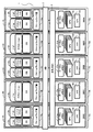
図2は、図1の情報処理システム1の構成の一例を示す図である。図2において、図1で示したものと同一のものは、同一の記号で示す。図2に示すように、情報処理システム1は、例えば、処理装置としての16台のシステムボード(SB:System Board)1A〜1Pと、4台のクロスバスイッチボックス2AB〜2DBとを有する。クロスバスイッチボックス2AB〜2DBがそれぞれ有するクロスバスイッチ2A〜2Dは、図1に示すクロスバスイッチ2に対応する。本実施の形態も、クロスバスイッチボックス2AB〜2DBは、ビルディングブロック構造である。
[Configuration of information processing system]
FIG. 2 is a diagram illustrating an example of the configuration of the
図2の例において、クロスバスイッチボックス2ABは、クロスバスイッチ2Aと、システム制御装置(SVP:SerVice Processor)V1とを有する。クロスバスイッチボックス2ABのシステム制御装置V1は、クロスバスイッチ2Aの状態監視、状態設定、及び、起動、停止制御等を行う。また、クロスバスイッチ2Aは、スイッチ2aとポートav、aw〜dv、dw、qv、qw、rv、rw、sv、swとスイッチ2aとを有する。スイッチ2aは、通信経路を切り替える。他のクロスバスイッチボックス2BB〜2DBの構成も同様である。
In the example of FIG. 2, the crossbar switch box 2AB includes a
また、図2の例において、それぞれのシステムボード1Aは、2つのクロスバスイッチ2Aとの接続用ポートax、ayを有する。また、クロスバスイッチ2Aも、各システムボード1Aとの2つの接続用ポートav、awを有する。即ち、各システムボード1Aは、2つの回線n1、n2によって、対応するクロスバスイッチ2Aに接続する。このように、図2に示すクロスバスイッチ2A〜2Dは、接続対称との間に二重の回線を有する対称型のクロスバスイッチである。二重の回線を有するため、クロスバスイッチ2A〜2Dは、片側の回線に障害が発生した場合であっても、残りの一つの回線を使用して動作することができる。
In the example of FIG. 2, each
この例において、第1、第2、第3、第4のシステムボード1A、1B、1C、1Dは、第1のクロスバスイッチ2Aに接続する。また、第5、第6、第7、第8のシステムボード1E、1F、1G、1Hは、第2のクロスバスイッチ2Bに接続する。また、第9、第10、第11、第12のシステムボード1I、1J、1K、1Lは、第3のクロスバスイッチ2Cに接続する。第13、第14、第15、第16のシステムボード1M、1N、1O、1Pは、第4のクロスバスイッチ2Dに接続する。
In this example, the first, second, third, and
また、図2の例において、第1のクロスバスイッチ2Aは、バスL1、L2によって、第2のクロスバスイッチ2Bと接続する。また、第1のクロスバスイッチ2Aは、バスL7、L8によって、第3のクロスバスイッチ2Cと接続する。また、第1のクロスバスイッチ2Aは、バスL9、L10によって、第4のクロスバスイッチ2Dと接続する。さらに、第2のクロスバスイッチ2Bは、バスL11、L12によって、第3のクロスバスイッチ2Cと接続し、第2のクロスバスイッチ2Bは、バスL3、L4によって、第4のクロスバスイッチ2Dと接続する。そして、第3のクロスバスイッチ2Cは、バスL5、L6によって、第4のクロスバスイッチ2Dと接続する。
In the example of FIG. 2, the
また、各システムボード1A〜1Pも、システム制御装置(図3にて図示)を有する。情報処理システム1における各クロスバスイッチボックス2AB〜2DBのシステム制御装置V1〜V4、及び、各システムボード1A〜1Pのシステム制御装置22は、内部バスL40によって互いに接続する。なお、図2において、情報処理システム1は、16台のシステムボード1A〜1Pと4台のクロスバスイッチ2A〜2Dとを有するが、システムボードの台数及びクロスバスイッチの台数は16台、4台に限定されない。続いて、各システムボード1A〜1Pの構成を説明する。
Each of the
[システムボードの構成]
図3は、図2に示したシステムボード1A〜1Pの構成の一例を説明する図である。図3の例では、システムボード1Aの構成を説明する。他のシステムボード1B〜1Pの構成も、システムボード1Aと同様である。図3に示すように、システムボード1Aは、システムボードユニットB1と、サービスプロセッサボードB2とを有する。
[System board configuration]
FIG. 3 is a diagram for explaining an example of the configuration of the
システムボードユニットB1は、例えば、複数のCPU(CPUチップ)12aと、システムコントローラ(System Controller)15と、I/Oコントローラ16と、PCI(Peripheral Component Interconnect) Express17と、メモリアクセスコントローラ18と、メモリ3、11aと、MBC(Maintenance Bus Controller 以下、MBCと称する)19とを有する。メモリ3、11aは、例えば、DRAM(Dynamic Random Access Memory)である。MBC19は、サービスプロセッサボードB2との通信経路を制御する。
The system board unit B1 includes, for example, a plurality of CPUs (CPU chips) 12a, a system controller (System Controller) 15, an I /
CPU12aは、図1で説明したアプリケーションpa、pbを実行する演算処理装置である。CPU12aの各々は、システムコントローラ15に接続する。システムコントローラ15は、メモリ3、11aに接続されたメモリアクセスコントローラ18に接続する。また、システムコントローラ15は、I/Oコントローラ16に接続する。I/Oコントローラ16は、例えば、外部メモリ(大容量メモリ及び/又はストレージ装置)やネットワークインタフェースカード(NIC)が接続されたPCI Express17と接続する。
The
そして、システムコントローラ15は、CPU12aとメモリアクセスコントローラ18との間の転送制御を行う。また、システムコントローラ15は、接続ポートax、ayを介して、クロスバスイッチ2Aに接続し、クロスバスイッチ2AとCPU12aとの間の転送制御、及び、クロスバスイッチ2Aとメモリアクセスコントローラ18との間の転送制御を行う。例えば、システムコントローラ15は、ブリッジ回路の役割を果たす。
Then, the
また、図1において、前述したとおり、メモリ3、11aの一部の領域はクロスバスイッチ2Aを介して共有され、共有メモリ3(図1)として使用され、他の一部の領域は、ローカルメモリ11aとして使用される。例えば、システムコントローラ15は、CPU12aが、別のシステムボードに搭載される共有メモリ3の領域にアクセスする場合、接続ポートax、ayを介して、クロスバスイッチ2Aに接続する。一方、CPU12aが、システムボード1Aに搭載されるメモリ3、11aの領域にアクセスする場合、システムコントローラ15は、メモリアクセスコントローラ18にアクセスする。
In FIG. 1, as described above, some areas of the
また、サービスプロセッサボードB2は、システム制御装置22とMBC(Maintenance Bus Controller 以下、MBCと称する)21を有する。システム制御装置22は、ノード内のハードウェアのアクセス制御、監視、電源投入、ログの採取、ユーザインターフェース制御(ユーザI/F)等の制御を行う。MBC21は、システムボードユニットB1との通信経路を制御する。また、MBC21は、CPU12aやメモリ3、11a、I/Oコントローラ16、システム制御装置22等のハードウェアから発生する割り込み要因を格納するレジスタrgを有する。また、図2で前述したとおり、システム制御装置22は、LAN(Local Area Network)などのネットワーク回線L40を介して、別のノードのシステム制御装置22、V1〜V4と相互に接続する。
The service processor board B2 includes a
なお、図3の例では、システムボード1A(1B〜1P)が4台のCPU(CPUチップ)12aを搭載する例を示したが、システムボード1Aが少なくとも1台のCPU12aを搭載する構成であっても良い。
In the example of FIG. 3, the example in which the
続いて、図3で説明したレジスタrgの具体例を説明する。 Subsequently, a specific example of the register rg described in FIG. 3 will be described.
[レジスタ]
図4は、図3のレジスタrgを説明する図である。図4の(A)は、プロセッサのレジスタマップrmの一例を示す図である。また、図4(B)は、それぞれの割り込み要因の説明図である。図3で示したとおり、各ノードのサービスプロセッサボードB2のMBC21は、レジスタrgを有する。また、レジスタrgは、ノードが有する複数の機能回路(CPU、メモリアクセスコントローラ、電源等を示す。以下、ハードウェアと称する)から発生する割り込み要因を格納する。図4の(A)のレジスタマップrmによると、レジスタrgは、例えば、割り込み要因CK、FE、IL、EC、SC、PM、LD、IIO、IMを格納する。ただし、割り込み要因は、図4の例に限定されるものではない。レジスタrgは、それぞれの割り込み要因を、レジスタマップrmに対応する所定のビット位置に格納する。
[register]
FIG. 4 is a diagram illustrating the register rg in FIG. FIG. 4A is a diagram illustrating an example of a register map rm of the processor. FIG. 4B is an explanatory diagram of each interrupt factor. As shown in FIG. 3, the
また、図4の(B)において、割り込み要因CKは、例えば、システム制御装置22のクロック制御エラーを示す。割り込み要因FEは、プロセッサにおいて発生した致命的な(FATAL)エラーを示す。また、割り込み要因ILは処理対象が不正である旨のエラー、割り込み要因ECはデバッグ時に使用する信号、割り込み要因SCはシステム制御装置22、V1〜V4から発生したリクエスト、割り込み要因PMは電源装置から発生したリクエストを示す。また、割り込み要因LDはクロスバスイッチ2の二重レーンの縮退に係るエラー、割り込み要因IIOはI/Oコントローラ16(図3)において発生するエラー、割り込み要因IMはメモリアクセスコントローラ18(図3)において発生するエラーを示す。
In FIG. 4B, the interrupt factor CK indicates, for example, a clock control error of the
続いて、障害発生時の処理を説明する。本実施の形態例では、以下に説明する障害発生処理において、レジスタrgを使用する。 Next, processing when a failure occurs will be described. In the present embodiment, the register rg is used in the failure occurrence process described below.
[障害発生処理]
図5は、図1〜図3で述べた、本実施の形態例における情報処理システム1の一部のノードにおいて障害が発生した場合の処理の流れを説明する図である。図5において、図2、図3で示したものと同一のものは、同一の記号で示す。
[Error handling]
FIG. 5 is a diagram for explaining the flow of processing when a failure occurs in some nodes of the
情報処理システム1の全体の障害解析を行う場合に、複数のノードのうち、1つのノードが主体となって障害解析を行う方が効率的である。効率化のために、情報処理システム1は、1つノードのシステム制御装置をマスターのシステム制御装置に、他のノードのシステム制御装置をスレーブのシステム制御装置に設定する。または、情報処理システム1は、マスターのシステム制御装置の切り替え用として、さらに、1つノードのシステム制御装置を、マスターの代替用のシステム制御装置に設定してもよい。図5の例おいて、例えば、マスターのシステム制御装置は、クロスバスイッチ2(図1)を有する1つのノード(図2の2AB)のシステム制御装置V1である。以下、マスターのシステム制御装置V1を、マスターノード2ABのシステム制御装置V1、スレーブのシステム制御装置22を、スレーブノード1A〜1P、2BB〜2DBのシステム制御装置22、V2〜V4と称する。
When performing failure analysis of the entire
前述したとおり、システム制御装置22、V1〜V4は各々、ノード内のハードウェアの状態の監視、及び、ハードウェアの制御を行う。また、システム制御装置22、V1〜V4は、ノード内の各ハードウェアから発生する割り込み要因を格納するレジスタrg(図4)を有する。ハードウェアの障害の一例としては、メモリ3、11aのデータ破損や、プロセッサ12aの内部障害等が挙げられる。
As described above, the
ハードウェアの障害が発生すると割り込み信号が発生し、割り込み要因がレジスタrgに格納される(図示の矢印x1)。システム制御装置22、V1〜V4は、レジスタrgを監視することによって、ハードウェアの障害の発生を検知すると、割り込み要因の発生をマスターノード2ABのシステム制御装置V1に通知する(図示の矢印x2、x3)。続いて、マスターノード2ABのシステム制御装置V1は、割り込み要因の発生の通知を受けると、各スレーブノード1A〜1P、2BB〜2DBのシステム制御装置22、V2〜V4に対して、ハードウェアのエラー情報を有するログ情報の送信を指示する(図示の矢印x4)。各スレーブノード1A〜1P、2BB〜2DBのシステム制御装置22、V2〜V4は、マスターノード2ABのシステム制御装置V1からの指示に応じて、ノード内のログ情報を収集しマスターノード2ABのシステム制御装置V1に送信する(図示の矢印x5)。そして、各ノードにおいて取得されたログ情報が、マスターノード2ABのシステム制御装置V1に収集される。
When a hardware failure occurs, an interrupt signal is generated and the interrupt factor is stored in the register rg (arrow x1 in the figure). When the
続いて、マスターノード2ABのシステム制御装置V1は、ログ情報の解析処理を行う。例えば、システム制御装置V1は、各ノードのログ情報に基づいて、障害ノード1B、及び、障害ノード1Bにおける障害部品を特定する。そして、システム制御装置V1は、ログ情報の解析処理によって特定された情報に基づいて、障害に対するリアクションを行う(図示の矢印x6、x7)。リアクションとは、例えば、各ノードで動作するアプリケーションに対する障害ノード1Bが有する共有メモリ3の領域へのアクセス抑止や、障害ノード1Bのハードウェアの停止制御である。
Subsequently, the system control device V1 of the master node 2AB performs log information analysis processing. For example, the system control device V1 identifies the failed
図5で説明してきたように、一部のノードで障害が発生した場合、マスターノード2ABのシステム制御装置V1は、各ノードにおいて収集されたログ情報を受信する。そして、マスターノード2ABのシステム制御装置V1は、取得した各ノードのログ情報を解析することによって、障害ノード、及び、障害が発生した回路の特定処理の後、障害に対するリアクションを行う。 As described with reference to FIG. 5, when a failure occurs in some nodes, the system control device V1 of the master node 2AB receives log information collected in each node. Then, the system control device V1 of the master node 2AB analyzes the acquired log information of each node, and performs a reaction to the failure after the specific processing of the failed node and the circuit in which the failure has occurred.
[ログ情報の解析]
図6は、図5において述べた、マスターノード2ABのシステム制御装置V1におけるログ情報の解析処理(S1)の概要を説明する図である。図6において、点線で囲む工程S3、S4は、本実施の形態例において付加される処理である。
[Analysis of log information]
FIG. 6 is a diagram for explaining the outline of the log information analysis process (S1) in the system controller V1 of the master node 2AB described in FIG. In FIG. 6, processes S3 and S4 surrounded by a dotted line are processes added in the present embodiment.
まず、ログ情報の解析処理(S1)を説明する。情報処理システム1は、障害が発生した場合、ノードの継続動作が可能な場合であっても、ノードの予防保守として障害の内容を特定する必要がある。また、情報処理システム1は、障害が発生しているASIC(Application Specific Integrated Circuit、以下、ASICと称する)部分を特定する必要がある。例えば、障害が発生しているASIC部分の特定、及び、ノードの継続動作の可否判定のために、マスターノード2ABのシステム制御装置V1は、ログ情報の解析処理を行う。この実施の形態では、ASICは、例えば、CPU、メモリアクセスコントローラ、I/Oコントローラに対応する。
First, the log information analysis process (S1) will be described. When a failure occurs, the
マスターノード2ABのシステム制御装置V1は、収集したログ情報に基づいてログ解析を行う(S1)。ログ情報とは、例えば、割り込み要因発生時のエラー情報を含むエラー要因情報と、エラーログ詳細情報である。エラーログ詳細情報とは、例えば、ASICの履歴情報やダンプ情報等である。エラーログ詳細情報はデータ量が膨大であるため、マスターノード2ABのシステム制御装置V1は、ログ情報(S1)内の各解析工程S61〜S65と平行して、エラーログ詳細情報を受信する。 The system control device V1 of the master node 2AB performs log analysis based on the collected log information (S1). The log information is, for example, error factor information including error information when an interrupt factor occurs, and error log detailed information. The error log detailed information is, for example, ASIC history information or dump information. Since the error log detailed information has an enormous amount of data, the system control device V1 of the master node 2AB receives the error log detailed information in parallel with the analysis steps S61 to S65 in the log information (S1).
続いて、工程S1における各解析工程を説明する。システム制御装置V1は、まず、エラー要因情報に基づいて、エラーコードの解析処理を行う(S61)。次に、システム制御装置V1は、ノードのハードウェアそれぞれを対象として、エラー要因情報に基づいて、障害の有無の判定、及び、障害部分の特定処理を行う(S62〜S65)。システム制御装置V1は、例えば、CPU12a、クロスバスイッチ2、メモリ3、11a等を対象として、エラー要因情報に基づいて、各ハードウェアにおける障害部分の判定、及び、障害部分の詳細の判定処理を行う。工程S62〜S65の処理により、障害ノード、及び、障害が発生している回路が特定され、他の回路が正常に動作していることが確認される。なお、図6の例において、システム制御装置V1は、CPU12a、クロスバスイッチ2、メモリ3、11aを対象として解析処理を行っているが、対象となるハードウェアは、この例に限定されるものではない。
Then, each analysis process in process S1 is demonstrated. The system control device V1 first performs error code analysis processing based on the error factor information (S61). Next, the system control device V1 determines whether or not there is a failure and specifies a failure portion based on the error factor information for each piece of hardware of the node (S62 to S65). The system control device V1, for example, for the
障害ノードの特定、及び、障害部分の特定が行われると、システム制御装置V1は、エラーログ詳細情報の収集の完了を待機して、エラーログ詳細情報の登録処理を行う(S66)。続いて、システム制御装置V1は、エラー要因情報に基づいて、障害部分に対応するログ情報を示す代表ログの登録処理を行う(S67)。エラーログ詳細情報、及び、代表ログは、障害の原因の分析や、障害の復旧に必要な情報である。ログ情報に基づく解析処理が完了すると、システム制御装置V1は、障害の重要度に応じて、情報処理システム1からの障害ノードの切り離し制御を行う(S2)。障害ノードの切り離し制御とは、例えば、障害ノードのハードウェアの電源停止を示す。
When the failure node is specified and the failure part is specified, the system control apparatus V1 waits for the completion of collection of the error log detailed information, and performs error log detailed information registration processing (S66). Subsequently, the system control device V1 performs a process of registering a representative log indicating log information corresponding to the failure portion based on the error factor information (S67). The error log detailed information and the representative log are information necessary for analyzing the cause of the failure and for recovering from the failure. When the analysis process based on the log information is completed, the system control device V1 performs the detachment control of the failed node from the
マスターノード2ABのシステム制御装置V1は、障害の重要度に関わらず、ログ情報の解析処理(S1)を実行する。また、ログ情報の解析処理では、ノード内のハードウェアそれぞれを対象として、詳細に障害部分の判定処理を行うため、時間を要する。また、エラーログ詳細情報の転送処理は、エラーログ詳細情報のデータ量が膨大であるため、時間を要する。このため、ログ情報の解析処理には、数十秒〜数分(30秒〜5分)程度の時間がかかる。即ち、障害の発生から障害ノードの切り離し制御まで、5分程度の時間を要する。 The system control device V1 of the master node 2AB executes the log information analysis process (S1) regardless of the importance of the failure. Further, the log information analysis processing takes time because the failure portion determination processing is performed in detail for each piece of hardware in the node. Also, the error log detailed information transfer process takes time because the data amount of the error log detailed information is enormous. For this reason, the log information analysis process takes about several tens of seconds to several minutes (30 seconds to 5 minutes). That is, a time of about 5 minutes is required from the occurrence of a failure to the separation control of the failed node.
しかしながら、情報処理システム1は、障害が発生してから短時間で運用を再開することが望ましい。運用の再開処理では、正常ノードが障害ノードの処理を引き継ぐため、情報処理システム1は、障害ノードを早急に特定する必要がある。また、複数のノード間でメモリを共有する情報処理システム1では、障害の発生に起因して、共有メモリ3の破損や不整合等の二次障害が発生する恐れがある。共有メモリ3に対する二次障害を抑止するために、早急に、障害ノードのメモリへのアクセス抑止を行うことが求められる。障害発生から障害ノードのメモリへのアクセス抑止まで、例えば、1秒程度で完了することが望ましい。
However, it is desirable for the
そこで、本実施の形態例において、マスターノード2ABのシステム制御装置V1は、ログ情報の解析処理(S1)の前に、FNL(Fail Node List、以下、FNLと称する)解析処理(S3)を行って障害ノードを特定し、障害ノードのメモリへのアクセス抑止を行う(S4)。 Therefore, in the present embodiment, the system controller V1 of the master node 2AB performs an FNL (Fail Node List, hereinafter referred to as FNL) analysis process (S3) before the log information analysis process (S1). The faulty node is identified and access to the memory of the faulty node is suppressed (S4).
本実施の形態例のマスターノード2ABのシステム制御装置V1は、他のノードの割り込み要因の発生に応じてレジスタrgの割り込み要因を受信し、割り込み要因のうち、障害として検出すべき割り込み要因を抽出する。そして、マスターノード2ABのシステム制御装置V1は、抽出結果に応じて障害ノードを特定し、障害ノードのメモリへのアクセスを抑止後、他のノードから受信したログ情報に基づいて障害ノードの切り離し制御を行う。 The system control device V1 of the master node 2AB according to the present embodiment receives the interrupt factor of the register rg in response to the occurrence of the interrupt factor of the other node, and extracts the interrupt factor to be detected as a fault from the interrupt factors. To do. Then, the system controller V1 of the master node 2AB identifies the failed node according to the extraction result, suppresses access to the memory of the failed node, and then controls the separation of the failed node based on the log information received from the other nodes. I do.
具体的に、マスターノード2ABのシステム制御装置V1は、FNL解析処理(S3)として、まず、発生中の割り込み要因を各ノードから取得する(S51)。続いて、システム制御装置V1は、取得した割り込み要因のうち、障害として検出すべき割り込み要因を抽出する(S52)。次に、システム制御装置V1は、抽出した割り込み要因のうち、波及先の割り込み要因をFNL解析の対象から除外する(S53)。即ち、システム制御装置V1は、抽出した割り込み要因のうち、別の割り込み要因に起因して発生した割り込み要因を、FNL解析処理の対象外とする。 Specifically, the system control device V1 of the master node 2AB first acquires the interrupt factor being generated from each node as the FNL analysis process (S3) (S51). Subsequently, the system control device V1 extracts an interrupt factor to be detected as a failure from the acquired interrupt factors (S52). Next, the system control device V1 excludes the spread interrupt factor from the FNL analysis targets among the extracted interrupt factors (S53). That is, the system control apparatus V1 excludes an interrupt factor generated due to another interrupt factor out of the extracted interrupt factors, as a target of FNL analysis processing.
続いて、システム制御装置V1は、複数の割り込み要因が抽出された場合、各割り込み要因の優先度を判定する(S54)次に、システム制御装置V1は、優先度の高い順に割り込み要因を選択し、割り込み要因に対応する障害ノードを特定する(S55)。次に、システム制御装置V1は、障害ノードの他ノードからのメモリへのアクセス抑止処理を行う(S56)。即ち、システム制御装置V1は、障害ノードが有する共有メモリ3の領域に対するアクセスを抑止する。各工程の詳細については、後述する。続いて、システム制御装置V1は、ログ情報の解析処理を実行し(S1)、障害ノードの情報処理システム1からの切り離し制御を行う(S2)。
Subsequently, when a plurality of interrupt factors are extracted, the system control device V1 determines the priority of each interrupt factor (S54). Next, the system control device V1 selects the interrupt factors in descending order of priority. Then, the faulty node corresponding to the interrupt factor is identified (S55). Next, the system control device V1 performs a process of suppressing access to the memory from the other node of the failed node (S56). That is, the system control device V1 suppresses access to the area of the shared
図6で説明してきたように、本実施の形態例において、システム制御装置V1は、FNL解析処理(S3)として、ログ情報の代わりに割り込み要因に基づいて、障害ノードを特定し、障害ノードのメモリに対する他ノードからのアクセス抑止処理を行う(図6のS56)。障害ノードのメモリに対するアクセスを抑止することによって、システム制御装置V1は、共有メモリ3の二次障害を早急に抑止し、障害発生時の障害ノードによる他ノードへの影響を低減する。
As described with reference to FIG. 6, in the present embodiment, the system control device V1 identifies the failed node based on the interrupt factor instead of the log information as the FNL analysis process (S3). A process of inhibiting access to the memory from another node is performed (S56 in FIG. 6). By suppressing access to the memory of the failed node, the system control device V1 quickly suppresses the secondary failure of the shared
そして、システム制御装置V1は、障害ノードのメモリへのアクセス抑止後、ログ情報の解析処理(S1)を行って、障害が発生しているASIC部分を特定し、ノードの継続動作の可否を判定する。そして、システム制御装置V1は、ログ情報の解析処理の結果に基づいて、障害ノードの情報処理システム1からの切り離し制御(S2)を行う。
Then, the system control device V1 performs log information analysis processing (S1) after suppressing access to the memory of the failed node, identifies the ASIC portion where the failure has occurred, and determines whether or not the node can continue operation. To do. Then, the system control device V1 performs detachment control (S2) of the failed node from the
図7は、図6のログ情報の解析処理(図6のS1)、及び、FNL解析処理(S3)に要する時間を例示する図である。図7の(A)は、ログ情報の解析処理(S1)から障害ノードの切り離し制御(S2)までの時間を示す図であって、図7の(B)は、FNL解析処理(S3)から障害ノードのメモリへのアクセス抑止処理(S4)までの時間を示す図である。 FIG. 7 is a diagram illustrating the time required for the log information analysis process (S1 in FIG. 6) and the FNL analysis process (S3) in FIG. FIG. 7A is a diagram showing the time from the log information analysis process (S1) to the failure node separation control (S2). FIG. 7B is a diagram showing the FNL analysis process (S3). It is a figure which shows the time until the access suppression process (S4) to the memory of a failure node.
図7の(A)では、ログ情報の解析処理(S1)の後、障害ノードの切り離し制御(S2)が行われる。前述したとおり、ログ情報の解析処理(S1)は、ハードウェアそれぞれに対するログ情報の解析処理やエラーログ詳細情報の転送処理に伴って、時間を要する。図7の(A)によると、障害発生から障害ノードの切り離し制御まで、期間t1に示す時間を要する。 In FIG. 7A, the failure node isolation control (S2) is performed after the log information analysis process (S1). As described above, the log information analysis process (S1) takes time with the log information analysis process and the error log detailed information transfer process for each piece of hardware. According to FIG. 7A, the time shown in the period t1 is required from the occurrence of a failure to the separation control of the failed node.
一方、図7の(B)において、FNL解析処理(S3)では、システム制御装置V1は、障害として検出すべき割り込み要因に基づいて障害ノードを特定する。また、FNL解析処理(S3)では、エラーログ詳細情報の転送が不要であり、割り込み要因(32ビット程度)のデータ量は小さい。したがって、システム制御装置V1は、障害ノードを早急に特定することが可能になるため、図7の(B)によると、障害発生から障害ノードのメモリへのアクセス抑止処理までの時間t2は、時間t1に対して大幅に短縮される。 On the other hand, in FIG. 7B, in the FNL analysis process (S3), the system control device V1 identifies the failure node based on the interrupt factor to be detected as a failure. Further, in the FNL analysis process (S3), it is not necessary to transfer detailed error log information, and the data amount of the interrupt factor (about 32 bits) is small. Accordingly, since the system control device V1 can quickly identify the failed node, according to FIG. 7B, the time t2 from the occurrence of the failure to the access suppression processing to the memory of the failed node is the time It is greatly shortened with respect to t1.
ここで、本実施の形態例におけるマスターノード2ABのシステム制御装置V1、及び、スレーブノード1A〜1P、2BB〜2DBのシステム制御装置22、V2〜V4のソフトウェアモジュール図を説明する。
Here, software module diagrams of the system controller V1 of the master node 2AB and the
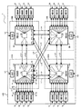
[ソフトウェアモジュール図]
図8は、本実施の形態における情報処理システムの各ノードのソフトウェアモジュール図である。図8は、マスターノード2ABのシステム制御装置V1、及び、スレーブノード1A〜1P、2BB〜2DBのシステム制御装置22、V2〜V4のブロック図を有する。初めに、スレーブノード1A〜1P、2BB〜2DBのシステム制御装置22、V2〜V4のブロックを説明する。ここでは、スレーブノード1Aのシステム制御装置22について説明する。
[Software module diagram]
FIG. 8 is a software module diagram of each node of the information processing system according to this embodiment. FIG. 8 includes a block diagram of the system control device V1 of the master node 2AB and the
図8において、スレーブノード1Aのシステム制御装置22は、例えば、FNL(Fail Node List)ドライバ54、FNL(Fail Node List)部50、ハード内制御部61、RAS(Reliability Availability Serviceability、以下、RASと称する)62、XSCF(eXtended System Control Facility、以下、XSCFと称する)コマンド部63、ハイパーバイザ64を有する。また、FNL部50は、例えば、FNL(Fail Node List)制御部51、FNL(Fail Node List)更新依頼受信制御部52、FNL(Fail Node List)更新部53を有する。
In FIG. 8, the
ハード内制御部61は、例えば、電源やプロセッサ(図8では、CPUと記す)やクロスバスイッチ(図8では、XBと記す)等のハードウェアに対するアクセス処理を行うHAP(Hardware Access Program、以下、HAPと称する)65を有する。そして、ハード内制御部61は、当該ハードウェアに対するアクセス処理における割り込み要因の発生を検知し、FNL部50のFNL更新依頼受信制御部52に通知する。また、RAS62は、ASICにおける割り込み要因の発生を検知し、FNL更新依頼受信制御部52に通知する。また、XSCFコマンド部43は、例えば、ハイパーバイザにおける割り込み要因の発生を検知し、FNL更新依頼受信制御部52に通知する。
The in-
また、FNL更新依頼受信制御部52は、各部からの割り込み要因の発生の通知を取得して、FNL制御部51に出力する。そして、FNL制御部51は、FNLドライバ54を介して、割り込み要因の発生をマスターノード2ABのシステム制御装置V1のFNL制御部32に通知する。また、FNL制御部51は、マスターノード2ABのシステム制御装置V1からの割り込み要因の収集依頼に応答して、発生している割り込み要因を収集しFNLドライバ54を介してマスターノード2ABのシステム制御装置V1に送信する。FNL更新部53は、マスターノード2ABのシステム制御装置V1からのFNL更新指示に基づいて、FNL(Fail Node List、図8には図示せず)を更新する。FNLとは、メモリを共有するノードそれぞれのアクセス処理の可否を管理するリストである。情報処理システム1における各ノードは、FNLに基づいて、アクセス抑止対象のノードを検知する。
In addition, the FNL update request
また、図8において、マスターノード2ABのシステム制御装置V1は、例えば、FNLドライバ35、FNL部30、XSCFコマンド部43、ハード内制御部41、RAS42、FNDB36(Fail Node DB、以下、FNDBと称する)を有する。また、FNL部30は、例えば、FNL解析部31、FNL制御部32、FNL更新部33、FNL更新依頼受信制御部34を有する。ハード内制御部41、RAS42、XSCFコマンド部43、FNL更新依頼受信制御部34の処理は、スレーブノード1Aのシステム制御装置22と同様である。
In FIG. 8, the system controller V1 of the master node 2AB includes, for example, an
FNL部30のFNL制御部32は、スレーブノード1Aのシステム制御装置22から割り込み要因発生の通知を受信すると、FNLドライバ35を介して、各スレーブノード1Aのシステム制御装置22に対して、発生中の割り込み要因の収集を指示する。FNL解析部31は、各ノードのシステム制御装置22から収集した割り込み要因に基づいて、FNDB36を参照し障害ノードを特定する。FNDB36は、FNL解析における解析論理の定義を有するファイルである。そして、FNL解析部31は、特定した障害ノードの情報に基づいて、各ノードのFNL更新部33にFNLの更新を指示する。
When the
図9は、図8において説明したFNL(Fail Node List)40の一例を示す図である。図9例において、情報処理システム1は、例えば、図2で示したように、16個のノードSB00〜SB15を有し、各ノードはメモリを共有する。そこで、図9のFNL40は、16個のノードそれぞれに対するアクセス処理の可否を管理する値を有する。例えば、値「0」の場合、対象ノードの共有メモリ3に対するアクセスが許可されることを示す。一方、値「1」の場合、対象ノードの共有メモリ3に対するアクセスが抑止されることを示す。
FIG. 9 is a diagram illustrating an example of an FNL (Fail Node List) 40 described in FIG. In the example of FIG. 9, the
続いて、割り込み要因が発生した後、図9において説明したFNL40が更新されるまでの処理の流れを、図8において説明したソフトウェアモジュールに対応して、時系列に説明する。
Next, the flow of processing from when an interrupt factor occurs until the
[ソフトウェアモジュールの処理の流れ]
図10は、割り込み要因が発生しFNLが更新される間のマスターノード2ABのシステム制御装置V1、及び、スレーブノード1Aのシステム制御装置22における、処理の流れを時系列に説明する図である。図10において、図8で示したものと同一のものは同一の記号で示してある。
[Software module processing flow]
FIG. 10 is a diagram for explaining the processing flow in time series in the system controller V1 of the master node 2AB and the
図10の例において、例えば、スレーブノードの一部のASICにおいて障害が発生する。障害の発生により割り込み信号が発生し、障害が発生したハードウェアに対応する割り込み要因がレジスタrgに登録される。スレーブノード1Aのシステム制御装置22は、障害の発生を検知すると(図示の矢印g1)、障害が発生したことをマスターノード2ABのシステム制御装置V1におけるハード内制御部41に通知する(図示の矢印g2)。
In the example of FIG. 10, for example, a failure occurs in some ASICs of the slave node. An interrupt signal is generated by the occurrence of a failure, and an interrupt factor corresponding to the hardware in which the failure has occurred is registered in the register rg. When the
システム制御装置V1におけるハード内制御部41は、障害の発生の通知を受けて、各スレーブノード1Aのシステム制御装置22に対して割り込み要因の収集を指示する(図示の矢印g3)。マスターノード2ABのシステム制御装置V1の通知に応答して、各スレーブノード1Aのシステム制御装置22は、発生している割り込み要因を、FNL部50を介して(図示の矢印g4)、システム制御装置V1のFNL部30に送信する(図示の矢印g5)。
In response to the notification of the occurrence of the failure, the in-
この結果、各スレーブノード1Aのシステム制御装置22の割り込み要因が収集される。割り込み要因のデータ量は小さい。このため、システム制御装置V1は、短時間で、各スレーブノード1Aのシステム制御装置22の割り込み要因を取得することができる。また、各システム制御装置22、V1〜V4間が高速通信を介して接続される場合、システム制御装置V1は、さらに、高速に、各システム制御装置22、V2〜V4の割り込み要因を取得することができる。
As a result, the interrupt factors of the
マスターノード2ABのシステム制御装置V1におけるFNL部30は、全てのスレーブノード1Aにおける割り込み要因を収集すると、FNL解析部31に解析処理を指示する(図示の矢印g6)。そして、FNL解析部31は、収集した割り込み要因に基づいて障害ノードを特定し、FNL部30に出力する(図示の矢印g7)。続いて、FNL部30は、障害ノードの情報に基づいて、各スレーブノード1Aのシステム制御装置のFNL部50にFNL40(図9)の更新を指示する(図示の矢印g8)。FNL40の更新指示を受信すると、スレーブノード1AのFNL部50は、FNL更新部53にFNL40の更新を実行させる(g9、g10)。
When the
図10のフローチャート図に示した処理の流れに基づいて、FNL解析処理、及び、FNLの更新処理が行われる。続いて、各処理の詳細をフローチャート図に基づいて説明する。 Based on the flow of processing shown in the flowchart of FIG. 10, FNL analysis processing and FNL update processing are performed. Next, details of each process will be described based on a flowchart.
[FNL解析処理、FNL更新処理]
図11は、図8の本実施の形態例におけるFNL解析部31の処理、及び、FNL更新部33の処理を説明するフローチャート図である。初めに、例えば、マスターノード2ABのシステム制御装置V1におけるFNL解析部31は、電源障害が発生しているか否かを判定する(S21)。電源障害が発生している場合、電源障害の対応が優先されるため、FNL解析部31は処理を終了する。
[FNL analysis processing, FNL update processing]
FIG. 11 is a flowchart for explaining the processing of the
一方、電源障害が発生していない場合(S21のNO)、FNL解析部31は、割り込み要因を取得する(S22)。前述したとおり、FNL解析部31は、割り込み要因が発生したノードからの通知に応答して、各ノードから割り込み要因を取得する。続いて、FNL解析部31は、収集された割り込み要因から、障害として検出すべき割り込み要因を抽出する(S23)。例えば、FNL解析部31は、例えば、割り込み要因のうち、ノードの停止が必要となる障害に対応する割り込み要因を抽出する。即ち、FNL解析部31は、ノードが継続して動作可能な割り込み要因を抽出の対処としない。
On the other hand, when a power failure has not occurred (NO in S21), the
本実施の形態例において、マスターノード2ABのシステム制御装置V1は、障害として検出すべき割り込み要因として、例えば、図4に例示した割り込み要因のうち、割り込み要因CK、FEを抽出する(S23)。割り込み要因CK、FEは、CPUが停止する障害要因であって、割り込み要因CK、FE以外の割り込み要因については機能の一部が縮退する故障要因であるためである。ただし、この例に限定されるものではなく、システム制御装置V1は、別の割り込み要因を、障害として検出すべき割り込み要因としてもよい。 In the present embodiment, the system controller V1 of the master node 2AB extracts, for example, interrupt factors CK and FE from the interrupt factors illustrated in FIG. 4 as interrupt factors to be detected as a failure (S23). This is because the interrupt factors CK and FE are failure factors that cause the CPU to stop, and interrupt factors other than the interrupt factors CK and FE are failure factors that cause part of the functions to be degraded. However, the present invention is not limited to this example, and the system control device V1 may use another interrupt factor as an interrupt factor to be detected as a failure.
なお、図4のレジスタマップrmは、プロセッサのレジスタマップである。情報処理システム1では、プロセッサのレジスタマップの他に、クロスバスイッチ用のレジスタマップやMBC用のレジスタマップが存在する。また、クロスバスイッチ用のレジスタに格納される割り込み要因については、例えば、複数の割り込み要因のうち、内部障害、及び、ポート障害に対応する割り込み要因が抽出対象となる。また、MBC用のレジスタに格納される割り込み要因については、例えば、複数の割り込み要因のうち、割り込み要因FEが抽出対象となる。
Note that the register map rm in FIG. 4 is a register map of the processor. In the
次に、FNL解析部31は、波及先の割り込み要因を抑止する(S24)。ここで、割り込み要因は、波及元の割り込み要因と、波及元の割り込み要因に基づいて誘発された波及先の割り込み要因とに区分される。FNL解析部31は、波及先の割り込み要因を除外して、波及元の割り込み要因のみに絞り込む。
Next, the
具体的に、例えば、あるノードのプロセッサにおいて障害が発生した場合、同一ノード内のクロスバスイッチの接続部や、プロセッサの他の部分に障害が波及することがある。この場合、プロセッサにおいて発生した障害に対応する割り込み要因が上位の割り込み要因、クロスバスイッチの接続部やプロセッサの他の部分において発生した障害に対応する割り込み要因が下位の割り込み要因に相当する。即ち、上位の割り込み要因が波及元の割り込み要因に該当し、下位の割り込み要因が波及先の割り込み要因に該当する。 Specifically, for example, when a failure occurs in a processor of a certain node, the failure may spill over to the connection part of the crossbar switch in the same node or another part of the processor. In this case, the interrupt factor corresponding to the fault that occurred in the processor corresponds to the higher interrupt factor, and the interrupt factor corresponding to the fault that occurred in the crossbar switch connection part or other part of the processor corresponds to the lower interrupt factor. That is, the higher interrupt factor corresponds to the transmission source interrupt factor, and the lower interrupt factor corresponds to the transmission destination interrupt factor.
FNL解析部31は、波及先の割り込み要因の抑止処理(S24)によって、波及先の割り込み要因をFNL解析の対象から除外するため、波及元の割り込み要因に対応するノードのみを障害ノードとして特定する。即ち、FNL解析部31は、波及先の割り込み要因に対応するノードを障害ノードして特定することを回避し、真に障害が発生するノードのみを、障害ノードとして特定する。
The
続いて、FNL解析部31は、抽出した割り込み要因それぞれの優先度を取得する(S25)。そして、FNL解析部31は、優先度の高い割り込み要因から順に、当該割り込み要因に対応して、障害ノードを特定すると共に、障害ノードに対する制御内容を取得する(S26)。そして、FNL更新部33、53は、取得した制御内容に基づいてFNL40を更新し、共有メモリ3上の障害ノードの領域への、他ノードからのアクセスを抑止する(S27)。続いて、FNL解析部31、及び、FNL更新部33、53は、次に優先度の高い割り込み要因を対象として、工程S26、S27の処理を行う。そして、FNL解析部31、及び、FNL更新部33、53は、抽出した全ての割り込み要因を対象として工程S26、S27の処理を行うと、FNLの解析処理、及び、FNLの更新処理を終了する。
Subsequently, the
続いて、図11のフローチャート図における波及先の割り込み要因の抑止処理(工程S24)の詳細を説明する。 Next, details of the spreading destination interrupt factor suppression process (step S24) in the flowchart of FIG. 11 will be described.
[波及先割り込み要因の抑止(図11の工程S24)]
図12は、波及先の割り込み要因の抑止処理を説明するフローチャート図である。まず、FNL解析部31は、FNDB36を参照し、抽出した割り込み要因(この例では、CK、FE)が、波及元の割り込み要因であるか否かを判定する(S11)。FNDB36については、次の図13に基づいて説明する。そして、抽出した割り込み要因が、下位の割り込み要因(波及先の割り込み要因)ではない場合(S12のNO)、即ち、波及元の割り込み要因である場合、FNL解析部31は波及先の割り込み要因の消し込み処理を終了する。
[Suppression of spreading destination interrupt factor (step S24 in FIG. 11)]
FIG. 12 is a flowchart for explaining the process of suppressing the spread interrupt factor. First, the
一方、抽出した割り込み要因が下位の割り込み要因である場合(S12のYES)、FNL解析部31は、各ノードのレジスタrgを参照し、当該下位の割り込み要因に対応する上位の割り込み要因を示す、波及元の割り込み要因が発生しているか否かを判定する(S13)。波及元の割り込み要因が発生している場合(S14のYES)、FNL解析部31は、下位の割り込み要因を抑止し、FNL解析処理の対象外とする(S15)。
On the other hand, when the extracted interrupt factor is a lower interrupt factor (YES in S12), the
一方、波及元の割り込み要因が発生していない場合(S14のNO)、FNL解析部31は波及先の割り込み要因の抑止処理を終了する。つまり、例えば、発生した割り込み要因が波及先の割り込み要因である場合であっても、波及元の割り込み要因が発生していない場合、FNL解析部31は、波及先の割り込み要因を抑止しない。
On the other hand, when the spillover interrupt factor has not occurred (NO in S14), the
図4、図12で述べてきたとおり、本実施の形態例では、FNL解析部31は、割り込み要因のうち、ノードの停止が必要となる障害に対応する割り込み要因に限定して、FNL解析を行う(図11のS23)。また、FNL解析部31は、さらに、波及元となる割り込み要因に限定して、FNL解析を行う(図11のS24)。したがって、FNL解析部31は、ノードの停止が必要となる障害に対応する割り込み要因であって、真に障害が発生しているノードにおける割り込み要因を抽出することができる。即ち、FNL解析部31は、ノードの停止が必要となる最小限の障害ノードを、効率的に特定することができる。
As described with reference to FIGS. 4 and 12, in the present embodiment, the
ここで、FNL解析部31が、FNL解析処理において参照するFNDB36の具体例を説明する。FNDB36は、FNL解析における解析論理の定義を有する。
Here, a specific example of the
[FNDBの具体例]
図13は、FNDB36の具体例を示す図である。図13の(A)は、FNL解析における解析論理を定義する定義テーブルtb1を示す図である。図13の(B)は、定義テーブルtb1に記述される各エントリの一部を説明する図である。定義テーブルtb1は、例えば、共通定義フレームとデータ定義ブロックとを有する。共通定義フレームは、定義テーブルtb1の版数や定義開始の宣言を有する。
[Specific example of FNDB]
FIG. 13 is a diagram illustrating a specific example of the
図13の(A)によると、定義テーブルtb1には、例えば、割り込み要因に対応して、優先度(prio)、アクション番号(act)、エントリ抑止条件(ent_dis)等の定義を有する。また、図13の(B)によると、優先度(prio)は、割り込み要因の優先度を示す。例えば、優先度は数値で示される。また、アクション番号(act)は、割り込み要因に対応する、障害ノード及び共有メモリへのアクセス抑止処理の種別を示す。アクセス抑止処理の種別の詳細については、別の図14に基づいて説明する。 According to FIG. 13A, the definition table tb1 has definitions of priority (prio), action number (act), entry suppression condition (ent_dis), etc., for example, corresponding to interrupt factors. Further, according to FIG. 13B, the priority (prio) indicates the priority of the interrupt factor. For example, the priority is indicated by a numerical value. The action number (act) indicates the type of processing for inhibiting access to the faulty node and the shared memory corresponding to the interrupt factor. Details of the type of access suppression processing will be described with reference to FIG.
そして、エントリ抑止条件(ent_dis)は、割り込み要因に対応して、当該割り込み要因に対して論理的に上位の割り込み要因を示す。即ち、エントリ抑止条件(ent_dis)は、割り込み要因に対応する、波及元の割り込み要因を示す。エントリ抑止条件(ent_dis)がブランクの場合、割り込み要因に対応する、波及元の割り込み要因が存在しないことを示す。 The entry suppression condition (ent_dis) indicates an interrupt factor logically higher than the interrupt factor corresponding to the interrupt factor. That is, the entry suppression condition (ent_dis) indicates a transmission source interrupt factor corresponding to the interrupt factor. When the entry suppression condition (ent_dis) is blank, it indicates that there is no transmission source interrupt factor corresponding to the interrupt factor.
FNL解析部31は、例えば、図13の定義テーブルtb1の記述cd1を参照して、波及先の割り込み要因の抑止処理(図11のS24)、優先度の取得処理(図11のS25)、障害ノードの特定、及び、アクセス抑止処理の取得処理(図11のS26)を行う。例えば、FNL解析部31は、定義テーブルtb1内のadrs(割り込み要因番号)列cd2を参照し、adrsの値が、割り込み要因に対応する割り込み要因番号と一致する行を探索する。
The
例えば、レジスタrgに基づいて収集した割り込み要因が、割り込み要因CKである場合を例に挙げる。割り込み要因CKは、図4のレジスタマップrmによると、1ビット目の位置に位置することから、割り込み要因CKに対応する割り込み要因番号は値「0x00000001」である。そこで、FNL解析部31は、割り込み要因CKに対応して、定義テーブルtb1における2行目の定義情報を検出する。なお、割り込み要因FEに対応する割り込み要因は値「0x00000003」である。そこで、FNL解析部31は、割り込み要因FEに対応して、定義テーブルtb1における1行目の定義情報を検出する。
For example, the case where the interrupt factor collected based on the register rg is the interrupt factor CK is taken as an example. According to the register map rm of FIG. 4, the interrupt factor CK is located at the position of the first bit, so the interrupt factor number corresponding to the interrupt factor CK is the value “0x00000001”. Therefore, the
続いて、FNL解析部31は、検出した2行目の定義情報のうち、エントリ抑止条件(ent_dis)に対応する項目cd5を参照する。図13の例において、2行目の定義情報におけるエントリ抑止条件(ent_dis)は、ブランクである。したがって、FNL解析部31は、割り込み要因CKを、波及元の割り込み要因として判定する(図11のS24)。また、FNL解析部31は、2行目の定義情報における優先度(prio)の項目cd3に基づいて、優先度「0x01」(図11のS25)を取得すると共に、アクション番号(act)の項目cd4に基づいてアクション番号「0x01」を取得する。なお、図13の例における優先度は、値が小さいほど高い。
Subsequently, the
一方、FNL解析部31は、割り込み要因FEに対応して、1行目の定義情報を検出する。図13の例において、定義テーブルtb1は、1行目の定義情報におけるエントリ抑止条件(ent_dis)として、定義“/XBBOX/XBUX/GXB/FN_XB_SND”の記述を有する(cd5)。それぞれの定義XBBOX、XBUX、GXB、FN_XB_SNDは、割り込み要因を示し、割り込み要因FEの波及元の割り込み要因に該当する。定義XBBOXは、例えば、クロスバボックスにおける割り込み要因を、定義FN_XB_SNDは、例えば、クロスバスイッチの送信部における割り込み要因を示す。したがって、FNL解析部31は、割り込み要因FEを波及先の割り込み要因として判定し、FNL解析の対象から除外する。
On the other hand, the
具体例に基づいて説明する。例えば、複数のノードSB00〜SB03が、クロスバスイッチ2を備えるノードXB00と接続する情報処理システムを例示する。具体例では、例えば、ノードSB02においてクロック制御エラーが発生すると共に、クロスバスイッチ2を備えるノードXB00において、ポート障害が発生する。
This will be described based on a specific example. For example, an information processing system in which a plurality of nodes SB00 to SB03 are connected to a node XB00 including the
いずれかの割り込み要因を検知すると、マスターノード2ABのシステム制御装置V1は、各ノードにおいて発生する割り込み要因を収集する(S22)。そして、システム制御装置V1は、ノードSB02において発生したクロック制御エラーに対応する割り込み要因CKと、ノードXB00において発生したポート障害に対応する対応する割り込み要因を取得する。具体例において、割り込み要因CK、及び、ポート障害に対応する割り込み要因は、抽出対象の割り込み要因である(S23)。 When any interrupt factor is detected, the system controller V1 of the master node 2AB collects the interrupt factors generated in each node (S22). Then, the system control device V1 acquires an interrupt factor CK corresponding to the clock control error that occurred in the node SB02 and a corresponding interrupt factor corresponding to the port failure that occurred in the node XB00. In the specific example, the interrupt factor CK and the interrupt factor corresponding to the port failure are the interrupt factors to be extracted (S23).
続いて、FNL解析部31は、図13のFNDB36を参照して(cd5)、各割り込み要因が波及元の割り込み要因であるか否かを判定する。図13において前述したとおり、割り込み要因CKは、波及元の割り込み要因である。また、図示していないが、具体例において、ポート障害に対応する割り込み要因は、波及元の割り込み要因である。このため、FNL解析部31は、ポート障害に対応する割り込み要因を抑止しない(S24)。次に、FNL解析部31は、FNDB36を参照して(cd3)、各割り込み要因に対応する優先度を取得する(S25)。図13において前述したとおり、割り込み要因CKの優先度(prio)は、優先度「0x01」である。また、具体例において、図示していないが、ポート障害に対応する割り込み要因の優先度は、優先度「0x05」である。したがって、FNL解析部31は、割り込み要因CKを、ポート障害に対応する割り込み要因よりも優先する。
Subsequently, the
続いて、図13の定義テーブルtb1のアクション番号(act)を説明する。アクション番号(act)は、割り込み要因に対応する、障害ノード及び共有メモリへのアクセス抑止処理の種別を示す。図13の定義テーブルtb1の記述cd4によると、割り込み要因CKのアクション番号(act)は、「0x01」である。また、図示していないが、ポート障害に対応する割り込み要因のアクション番号(act)は、例えば、「0x12」である。次の図14に基づいて、アクション番号(act)に対応する制御情報について説明する。 Next, the action number (act) in the definition table tb1 in FIG. 13 will be described. The action number (act) indicates the type of processing for inhibiting access to the failed node and shared memory corresponding to the interrupt factor. According to the description cd4 of the definition table tb1 in FIG. 13, the action number (act) of the interrupt factor CK is “0x01”. Although not shown, the action number (act) of the interrupt factor corresponding to the port failure is, for example, “0x12”. The control information corresponding to the action number (act) will be described based on FIG.
図14は、アクション番号(act)を有する定義テーブルtb2の具体例を示す図である。図14の(A)は、アクション番号(act)に対応して制御情報(rule)の記述を有する定義テーブルtb2を示す図であって、図14の(B)は、定義テーブルtb2に記述される制御情報(rule)の各エントリの一部を説明する図である。FNDB36は、例えば、図13の定義テーブルtb1に加えて、図14に示す定義テーブルtb2を有する。定義テーブルtb2は、例えば、定義テーブルtb2の版数や定義開始の宣言を有する共通定義フレームと、データ定義ブロックとを有する。
FIG. 14 is a diagram illustrating a specific example of the definition table tb2 having an action number (act). FIG. 14A shows a definition table tb2 having a description of control information (rule) corresponding to the action number (act), and FIG. 14B is described in the definition table tb2. It is a figure explaining a part of each entry of control information (rule). For example, the
図14の定義テーブルtb2のデータ定義ブロックは、アクション番号(act)に対応して、障害ノードに対する制御情報(rule)の記述cd6を有する。例えば、定義テーブルtb2は、アクション番号(act)「0x01」に対応して、制御情報(rule)として、エントリFNL_UPDATEを有する。また、定義テーブルtb2は、アクション番号(act)「0x02」に対応して、制御情報(rule)として、エントリFNL_UPDATE_DESTを有する。同様にして、定義テーブルtb2は、アクション番号(act)「0x11」に対応して、制御情報(rule)として、エントリGCSM_DEGRADEを、アクション番号(act)「0x12」に対応して、制御情報(rule)として、エントリGCSM_DEGRADE_DESTを有する。 The data definition block of the definition table tb2 in FIG. 14 has a description cd6 of control information (rule) for the failed node corresponding to the action number (act). For example, the definition table tb2 has an entry FNL_UPDATE as control information (rule) corresponding to the action number (act) “0x01”. Further, the definition table tb2 has an entry FNL_UPDATE_DEST as control information (rule) corresponding to the action number (act) “0x02”. Similarly, the definition table tb2 corresponds to the action number (act) “0x11”, and the control information (rule) includes the entry GCSM_DEGRADE, and the action number (act) “0x12” corresponds to the control information (rule). ) As an entry GCSM_DEGRADE_DEST.
図14の(B)によると、エントリFNL_UPDATEは、割り込み要因が検出されたノードを障害ノードとして特定し、当該障害ノードを停止対象のノードとしてメモリアクセスの制御を行うことを示す。この場合、マスターノード2ABのシステム制御装置V1は、例えば、割り込み要因が検出されたノード(障害ノード)の共有メモリ3内の領域に対する、他のノードからのアクセスを抑止する。アクセスが抑止されることにより、障害ノードのメモリが共有メモリから切り離され、情報処理システムの継続稼動が可能になる。また、図14の(B)によると、エントリFNL_UPDATE_DESTは、割り込み要因が検出されたノードに接続されたノードを障害ノードとして特定し、当該障害ノードを停止対象のノードとしてメモリアクセスの制御を行うことを示す。
According to FIG. 14B, the entry FNL_UPDATE indicates that the node in which the interrupt factor is detected is identified as a failed node, and the memory access is controlled with the failed node as a node to be stopped. In this case, for example, the system controller V1 of the master node 2AB suppresses access from other nodes to the area in the shared
さらに、エントリGCSM_DEGRADEは、割り込み要因が検出されたノードを障害ノードとして特定し、当該障害ノードを機能縮退対象のノードとしてメモリアクセスの制御を行うことを示す。さらに、エントリGCSM_DEGRADE_DESTは、割り込み要因が検出されたノードに接続されたノードを障害ノードとして特定し、当該障害ノードを機能縮退対象のノードとしてメモリアクセスの制御を行うことを示す。障害ノードの機能縮退とは、例えば、障害ノードがクロスバスイッチ2を備えるノードである場合に、図2で説明したクロスバスイッチの二重の回線を一回線に縮退させる制御を示す。
Further, the entry GCSM_DEGRADE indicates that the node in which the interrupt factor is detected is identified as a failure node, and the memory access is controlled by using the failure node as a node subject to function degradation. Further, the entry GCSM_DEGRADE_DEST indicates that the node connected to the node where the interrupt factor is detected is identified as a failed node, and memory access is controlled using the failed node as a function degradation target node. For example, when the failure node is a node provided with the
具体例において、前述したとおり、割り込み要因CKのアクション番号(act)は、値「0x01」であって、ポート障害に対応する割り込み要因のアクション番号(act)は、例えば、値「0x12」である。したがって、FNL解析部31は、割り込み要因CKに対応して割り込み要因が発生したノードSB02を障害ノードとして特定する。そして、FNL更新部33、53は、ノードSB02に係るメモリアクセスの制御(FNL_UPDATE)を行う。また、FNL解析部31は、ポート障害に対応する割り込み要因が発生したノードXB00に接続されるノードSB00〜SB03を障害ノードとして特定する。そして、FNL更新部33、53は、ノードSB00〜SB00に係る機能縮退制御(GCSM_DEGRADE_DEST)を行う。
In the specific example, as described above, the action number (act) of the interrupt factor CK is the value “0x01”, and the action number (act) of the interrupt factor corresponding to the port failure is, for example, the value “0x12”. . Therefore, the
ただし、具体例において、割り込み要因CKは、ポート障害に対応する割り込み要因よりも優先される。そこで、FNL更新部33、53は、まず、割り込み要因CKに対応する障害ノードのメモリへのアクセス抑止処理を行う(S26、S27)。例えば、それぞれのノードのFNL更新部33、53はFNL40を更新し、ノードSB02のメモリに対する他のノードからのアクセスを抑止する。
However, in the specific example, the interrupt factor CK is prioritized over the interrupt factor corresponding to the port failure. Therefore, the
続いて、FNL更新部33、53は、ポート障害に対応する割り込み要因に対応して、ノードSB00〜SB03のメモリへのアクセス抑止処理を行う(S26、S27)。例えば、それぞれのノードのFNL更新部33、53はFNL40を更新し、ノードXB00からノードSB00〜SB03に対するアクセス処理における二重の回線を片側の回線に縮退させる。回線が縮退されたことにより、ノードSB00〜SB03の共有メモリに対するアクセス経路が減少する。
Subsequently, the
図15は、具体例におけるメモリの抑止範囲を説明する図である。具体例によると、ノードSB02においてクロック制御エラーが発生した場合、他ノードによる、ノードSB02の共有メモリ3に対するアクセスが抑止される(ac1)。一方、ノードXB00においてポート障害が発生した場合、ノードXB00とノードSB00〜SB03との間の回線が片側に縮退される(ac2)。即ち、図15の例において、回線n1、n3、n5、n7が使用できない状態となる。なお、例えば、回線n1、n3、n5、n7が既に停止されている状態で、さらに、ポート障害が発生した場合、全ての回線n1〜n8が使用不可状態となり、ノードSB00〜SB03の共有メモリ3に対するアクセスが行えなくなる。
FIG. 15 is a diagram illustrating a memory suppression range in a specific example. According to a specific example, when a clock control error occurs in the node SB02, access to the shared
図15に示すように、割り込み要因CKに対応するアクセスの抑止範囲は、クロスバスイッチ2のポート障害によるアクセスの抑止範囲より狭い。図15の例では、アクセスの抑止範囲のより広いポート障害に対応する割り込み要因の優先度が低く設定されることにより、ポート障害によるアクセス抑止処理は、割り込み要因CKによるアクセス抑止処理より後から行われる。アクセスの抑止範囲の広い割り込みがより後から行われることによって、情報処理システム1の性能がより長時間維持される。図15の例のように、例えば、割り込み要因の優先度は、システム制御装置1の性能をより高性能に維持するために、抑止範囲がより小さい割り込み要因ほど、より高い優先度が設定される。
As shown in FIG. 15, the access inhibition range corresponding to the interrupt factor CK is narrower than the access inhibition range due to the port failure of the
以上のように、本実施の形態例における情報処理システムは、ノードの各々は、複数の機能回路と機能回路を制御する制御装置と、複数の機能回路から発生する割り込み要因を格納するレジスタとを有する。また、情報処理システムにおける複数のノードのうちの1のノードの制御装置は、他のノードの割り込み要因の発生に応じてレジスタの割り込み要因を受信し、割り込み要因のうち、障害として検出すべき割り込み要因を抽出して、抽出結果に応じて障害ノードを特定する。そして、制御装置は、障害ノードのメモリへのアクセスを抑止後、他のノードから受信したログ情報に基づいて障害ノードの切り離し制御を行う。 As described above, in the information processing system according to the present embodiment, each node includes a plurality of functional circuits, a control device that controls the functional circuits, and a register that stores interrupt factors generated from the plurality of functional circuits. Have. In addition, the control device of one node of the plurality of nodes in the information processing system receives the interrupt factor of the register in response to the occurrence of the interrupt factor of the other node, and among the interrupt factors, the interrupt to be detected as a failure A factor is extracted, and a faulty node is specified according to the extraction result. Then, after the control device suppresses access to the memory of the failed node, it performs detachment control of the failed node based on the log information received from other nodes.
本実施の形態例における情報処理システムは、割り込み要因に基づくことにより障害ノードを高速に特定することができる。また、本実施の形態例における情報処理システムは、複数の割り込み要因のうち、ノードの停止が必要となる、障害として検出すべき割り込み要因を対象として、障害ノードを特定するため、より効率的に、障害ノードを特定することができる。 The information processing system in the present embodiment can identify a failed node at high speed based on an interrupt factor. In addition, the information processing system according to the present embodiment is more efficient because it identifies a faulty node for an interrupt factor that should be detected as a fault that requires a node to stop among a plurality of interrupt factors. The failure node can be identified.
また、本実施の形態例における情報処理システムは、高速に、障害ノードを特定することができるため、障害ノードのメモリへのアクセスを早急に抑止することができ、共有メモリへの二次障害を回避することができる。即ち、情報処理システムは、障害発生時に障害ノードによる他ノードの影響を早急に低減することができる。また、情報処理システムは、障害ノードを高速に特定できるため、障害の発生時における、障害ノードから正常ノードへの運用の切り替えにかかるオーバヘッドを低減できる。 In addition, since the information processing system according to the present embodiment can identify a failed node at high speed, it is possible to quickly prevent access to the memory of the failed node, and to prevent a secondary failure to the shared memory. It can be avoided. That is, the information processing system can quickly reduce the influence of other nodes due to the failed node when a failure occurs. Further, since the information processing system can identify the failed node at high speed, it is possible to reduce the overhead required for switching the operation from the failed node to the normal node when a failure occurs.
また、本実施の形態例における情報処理システムにおいて、1のノードの制御装置は、障害として検出すべき割り込み要因の波及元となる割り込み要因が発生しているか否かを判定し、発生していない場合に、割り込み要因に対応するノードを障害ノードとして特定し、発生している場合に、波及元となる割り込み要因に対応するノードを障害ノードとして特定する。 Further, in the information processing system according to the present embodiment, the control device of one node determines whether or not an interrupt factor that is a transmission source of the interrupt factor to be detected as a failure has occurred, and has not occurred. In such a case, the node corresponding to the interrupt factor is specified as a faulty node.
本実施の形態例における情報処理システムは、波及元となる割り込み要因に対応するノードを障害ノードとして特定することにより、複数の割り込み要因が連動して発生している場合に、複数の割り込み要因のうち、波及元の割り込み要因のみを対象として、当該波及元の割り込み要因に対応する障害ノードを特定することができる。 The information processing system according to the present exemplary embodiment identifies a node corresponding to an interrupt factor as a transmission source as a failure node, so that when a plurality of interrupt factors are generated in conjunction with each other, Among them, the failure node corresponding to the transmission source interrupt factor can be identified only for the transmission source interrupt factor.
また、本実施の形態例における情報処理システムにおいて、第1のノードの制御部は、障害として検出すべき割り込み要因を複数抽出した場合に、割り込み要因の優先度に基づいて、特定した障害ノードのメモリへのアクセスを抑止する。 Further, in the information processing system according to the present embodiment, when the control unit of the first node extracts a plurality of interrupt factors to be detected as a failure, the control unit of the identified failure node is based on the priority of the interrupt factor. Suppresses access to memory.
本実施の形態例における情報処理システムは、割り込み要因の優先度に基づいて、障害ノードのメモリへのアクセスの抑止処理の順を制御するため、割り込み要因に応じて、障害ノードのメモリへのアクセスの抑止処理の順を調整することができる。また、情報処理システムは、メモリへのアクセス抑止範囲の広い割り込み要因の優先度を低く設定することによって、情報処理システムの性能をより長く維持することができる。 The information processing system according to the present embodiment controls the order of processing for inhibiting access to the memory of the faulty node based on the priority of the interrupt factor, and therefore accesses the memory of the faulty node according to the interrupt factor. The order of the suppression processing can be adjusted. In addition, the information processing system can maintain the performance of the information processing system for a longer time by setting the priority of the interrupt factor having a wide range of inhibiting access to the memory to a low level.
また、本実施の形態例における情報処理システムにおいて、1のノードの制御装置は、障害として検出すべき割り込み要因がデータ処理を実行するノードにおいて発生した割り込み要因である場合に、発生元のノードを障害ノードとして特定する。また、1のノードの制御装置は、障害として検出すべき割り込み要因が網結合装置を備えるノードにおいて発生した割り込み要因である場合に、網結合装置に接続されたノードを障害ノードとして特定する。このため、本実施の形態例における情報処理システムは、割り込み要因に基づいて、割り込み要因に対応する障害ノードを特定することができる。 Further, in the information processing system according to the present embodiment, the control device of one node determines the source node when the interrupt factor that should be detected as a failure is an interrupt factor that occurred in the node that executes data processing. Identify as failed node. In addition, when the interrupt factor to be detected as a failure is an interrupt factor generated in a node including the network coupling device, the control device of one node identifies the node connected to the network coupling device as the fault node. For this reason, the information processing system according to the present embodiment can identify the failed node corresponding to the interrupt factor based on the interrupt factor.
また、本実施の形態例における情報処理システムにおいて、1のノードは、割り込み要因と、割り込み要因の波及元となる割り込み要因との対応関係を有する定義テーブルを有し、1のノードの制御装置は、定義テーブルに基づいて、障害として検出すべき割り込み要因の波及元となる割り込み要因が発生しているか否かを判定する。 Further, in the information processing system according to the present embodiment, one node has a definition table having a correspondence relationship between an interrupt factor and an interrupt factor as a transmission source of the interrupt factor, and the control device of the one node is Based on the definition table, it is determined whether or not an interrupt factor that is the source of the interrupt factor to be detected as a failure has occurred.
本実施の形態例における情報処理システムは、割り込み要因と、割り込み要因の波及元となる割り込み要因との対応関係を有する定義テーブルを有することによって、波及元の割り込み要因であるか否かを高速に判定することができる。また、情報処理システムは、割り込み要因が増加した場合や、変更が発生した場合に、定義テーブルの更新処理を行うことで、割り込み要因の増加や変更を簡易に適用することができる。これにより、情報処理システムは、エンハンスや設計変更時におけるメンテナンス工数を小さく抑えることができる。 The information processing system according to the present embodiment has a definition table having a correspondence relationship between an interrupt factor and an interrupt factor that is the source of the interrupt factor, so that it is possible to determine whether the interrupt factor is the source of the transmission at high speed. Can be determined. Further, the information processing system can easily apply the increase or change of the interrupt factor by updating the definition table when the interrupt factor increases or when a change occurs. Thereby, the information processing system can keep maintenance man-hours small at the time of enhancement or design change.
また、本実施の形態例における情報処理システムは、割り込み要因に対応して優先度を有する定義テーブルを有し、1のノードの前記制御装置は、定義テーブルに基づいて、割り込み要因の優先度を判定する。 The information processing system according to the present embodiment has a definition table having a priority corresponding to the interrupt factor, and the control device of one node sets the priority of the interrupt factor based on the definition table. judge.
本実施の形態例における情報処理システムは、割り込み要因に対応して優先度を有する定義テーブルを有することによって、割り込み要因の優先度を高速に取得することができる。また、情報処理システムは、割り込み要因が増加した場合や、変更が発生した場合に、定義テーブルの更新処理を行うことで、割り込み要因の増加や変更を簡易に適用することができる。これにより、情報処理システムは、エンハンスや設計変更時におけるメンテナンス工数を小さく抑えることができる。 The information processing system according to the present embodiment can obtain the priority of the interrupt factor at high speed by including the definition table having the priority corresponding to the interrupt factor. Further, the information processing system can easily apply the increase or change of the interrupt factor by updating the definition table when the interrupt factor increases or when a change occurs. Thereby, the information processing system can keep maintenance man-hours small at the time of enhancement or design change.
以上、各ノードが共有メモリを有する分散型共有メモリの構成を例に説明したが、本実施の形態は、各ノードが共有メモリを設けておらず、各ノードとは別に共有メモリを備えるクラスター型構成にも適用可能である。 As described above, the configuration of a distributed shared memory in which each node has a shared memory has been described as an example. However, in this embodiment, each node does not have a shared memory, and a cluster type in which a shared memory is provided separately from each node. It is also applicable to the configuration.
以上の実施の形態をまとめると、次の付記のとおりである。 The above embodiment is summarized as follows.
(付記1)
複数のノード間でメモリを共有する情報処理システムにおいて、
前記ノードの各々は、
複数の機能回路と前記機能回路を制御する制御装置と、
前記複数の機能回路から発生する割り込み要因を格納するレジスタとを有し、
前記複数のノードのうちの1のノードの前記制御装置は、
他の前記ノードの割り込み要因の発生に応じて前記レジスタの前記割り込み要因を受信し、前記割り込み要因のうち、障害として検出すべき割り込み要因を抽出して、抽出結果に応じて障害ノードを特定し、前記障害ノードの前記メモリへのアクセスを抑止後、前記他のノードから受信したログ情報に基づいて前記障害ノードの切り離し制御を行う情報処理システム。
(Appendix 1)
In an information processing system that shares memory among multiple nodes,
Each of the nodes is
A plurality of functional circuits and a control device for controlling the functional circuits;
A register storing interrupt factors generated from the plurality of functional circuits,
The control device of one of the plurality of nodes is
The interrupt factor of the register is received according to the occurrence of the interrupt factor of the other node, the interrupt factor to be detected as a fault is extracted from the interrupt factors, and the faulty node is identified according to the extraction result An information processing system that performs detachment control of the failed node based on log information received from the other node after inhibiting the failed node from accessing the memory.
(付記2)
付記1において、
前記他のノードの前記制御装置は、前記レジスタの前記割り込み要因の発生を前記1のノードの制御装置に通知し、
前記1のノードの制御装置は、前記他のノードからの前記通知に応じて、前記他ノードの前記レジスタの割り込み要因と前記ログ情報とを収集する情報処理システム。
(Appendix 2)
In
The control device of the other node notifies the control device of the one node of the occurrence of the interrupt factor of the register,
The control device of the one node collects an interrupt factor and the log information of the register of the other node in response to the notification from the other node.
(付記3)
付記1または2において、
前記1のノードは、網結合装置を備え、
前記他のノードは、データ処理を実行し、前記網結合装置を介して前記メモリにアクセスする処理装置を備える情報処理システム。
(Appendix 3)
In
The one node includes a network coupling device,
An information processing system comprising: a processing device that performs data processing and accesses the memory via the network coupling device.
(付記4)
付記1乃至3のいずれかにおいて、
前記1のノードの前記制御装置は、前記障害として検出すべき割り込み要因の波及元となる割り込み要因が発生しているか否かを判定し、発生していない場合に、前記割り込み要因に対応するノードを前記障害ノードとして特定し、発生している場合に、前記波及元となる割り込み要因に対応するノードを前記障害ノードとして特定する情報処理システム。
(Appendix 4)
In any one of
The control device of the one node determines whether or not an interrupt factor as a transmission source of the interrupt factor to be detected as the failure has occurred, and if not, the node corresponding to the interrupt factor Is identified as the faulty node, and if it has occurred, an information processing system that identifies as the faulty node a node corresponding to the interrupt factor serving as the transmission source.
(付記5)
付記1乃至4のいずれかにおいて、
前記第1のノードの前記制御部は、前記障害として検出すべき割り込み要因を複数抽出した場合に、前記割り込み要因の優先度に基づいて、前記特定した障害ノードの前記メモリへのアクセスを抑止する情報処理システム。
(Appendix 5)
In any one of
When the control unit of the first node extracts a plurality of interrupt factors to be detected as the failure, the control unit suppresses access to the memory of the specified failure node based on the priority of the interrupt factor. Information processing system.
(付記6)
付記3において、
前記1のノードの前記制御装置は、前記障害として検出すべき割り込み要因が前記データ処理を実行するノードにおいて発生した割り込み要因である場合に、発生元のノードを前記障害ノードとして特定し、前記障害として検出すべき割り込み要因が前記網結合装置を備えるノードにおいて発生した割り込み要因である場合に、前記網結合装置に接続されたノードを前記障害ノードとして特定する情報処理システム。
(Appendix 6)
In
When the interrupt factor to be detected as the fault is an interrupt factor generated in the node executing the data processing, the control device of the one node identifies the source node as the fault node, and An information processing system that identifies a node connected to the network coupling device as the failed node when the interrupt factor to be detected as is an interrupt factor generated in a node including the network coupling device.
(付記7)
付記4において、
前記1のノードは、
前記割り込み要因と、前記割り込み要因の波及元となる割り込み要因との対応関係を有する定義テーブルを有し、
前記1のノードの前記制御装置は、前記定義テーブルに基づいて、前記障害として検出すべき割り込み要因の波及元となる割り込み要因が発生しているか否かを判定する情報処理システム。
(Appendix 7)
In Appendix 4,
The one node is
A definition table having a correspondence relationship between the interrupt factor and the interrupt factor that is the source of the interrupt factor;
The information processing system according to
(付記8)
付記5において、
前記1のノードは、
前記割り込み要因に対応して前記優先度を有する定義テーブルを有し、
前記1のノードの前記制御装置は、前記定義テーブルに基づいて、割り込み要因の前記優先度を判定する情報処理システム。
(Appendix 8)
In Appendix 5,
The one node is
A definition table having the priority corresponding to the interrupt factor;
The information processing system in which the control device of the one node determines the priority of an interrupt factor based on the definition table.
(付記9)
付記1乃至8のいずれかにおいて、
前記メモリは各前記ノード内に設けられた情報処理システム。
(Appendix 9)
In any one of
The memory is an information processing system provided in each node.
(付記10)
複数のノード間でメモリを共有する情報処理システムの障害処理方法において、
前記ノードの各々は、
複数の機能回路と前記機能回路を制御する制御装置と、
前記複数の機能回路から発生する割り込み要因を格納するレジスタとを有し、
前記複数のノードのうちの1のノードの前記制御装置は、
他の前記ノードの割り込み要因の発生に応じて前記レジスタの前記割り込み要因を受信し、前記割り込み要因のうち、障害として検出すべき割り込み要因を抽出して、抽出結果に応じて障害ノードを特定し、前記障害ノードの前記メモリへのアクセスを抑止後、前記他のノードから受信したログ情報に基づいて前記障害ノードの切り離し制御を行う情報処理システムの障害処理方法。
(Appendix 10)
In a failure processing method for an information processing system that shares memory among multiple nodes,
Each of the nodes is
A plurality of functional circuits and a control device for controlling the functional circuits;
A register storing interrupt factors generated from the plurality of functional circuits,
The control device of one of the plurality of nodes is
The interrupt factor of the register is received according to the occurrence of the interrupt factor of the other node, the interrupt factor to be detected as a fault is extracted from the interrupt factors, and the faulty node is identified according to the extraction result A failure processing method of an information processing system that performs detachment control of the failed node based on log information received from the other node after inhibiting the failed node from accessing the memory.
(付記11)
付記10において、
前記他のノードの前記制御装置は、前記レジスタの前記割り込み要因の発生を前記1のノードの制御装置に通知し、
前記1のノードの制御装置は、前記他のノードからの前記通知に応じて、前記他ノードの前記レジスタの割り込み要因と前記ログ情報とを収集する情報処理システムの障害処理方法。
(Appendix 11)
In
The control device of the other node notifies the control device of the one node of the occurrence of the interrupt factor of the register,
The failure processing method of the information processing system, wherein the control device of the one node collects the interrupt factor of the register of the other node and the log information in response to the notification from the other node.
(付記12)
付記10または11において、
前記1のノードは、網結合装置を備え、
前記他のノードは、データ処理を実行し、前記網結合装置を介して前記メモリにアクセスする処理装置を備える情報処理システムの障害処理方法。
(Appendix 12)
In
The one node includes a network coupling device,
A failure processing method for an information processing system comprising: a processing device that executes data processing and accesses the memory via the network coupling device.
(付記13)
付記10乃至12のいずれかにおいて、
前記1のノードの前記制御装置は、前記障害として検出すべき割り込み要因の波及元となる割り込み要因が発生しているか否かを判定し、発生していない場合に、前記割り込み要因に対応するノードを前記障害ノードとして特定し、発生している場合に、前記波及元となる割り込み要因に対応するノードを前記障害ノードとして特定する情報処理システムの障害処理方法。
(Appendix 13)
In any one of
The control device of the one node determines whether or not an interrupt factor as a transmission source of the interrupt factor to be detected as the failure has occurred, and if not, the node corresponding to the interrupt factor A fault processing method of an information processing system that specifies a node corresponding to an interrupt factor that is a transmission source as the faulty node.
(付記14)
付記10乃至13のいずれかにおいて、
前記第1のノードの前記制御部は、前記障害として検出すべき割り込み要因を複数抽出した場合に、前記割り込み要因の優先度に基づいて、前記特定した障害ノードの前記メモリへのアクセスを抑止する情報処理システムの障害処理方法。
(Appendix 14)
In any one of
When the control unit of the first node extracts a plurality of interrupt factors to be detected as the failure, the control unit suppresses access to the memory of the specified failure node based on the priority of the interrupt factor. A failure processing method for an information processing system.
(付記15)
付記12において、
前記1のノードの前記制御装置は、前記障害として検出すべき割り込み要因が前記データ処理を実行するノードにおいて発生した割り込み要因である場合に、発生元のノードを前記障害ノードとして特定し、前記障害として検出すべき割り込み要因が前記網結合装置を備えるノードにおいて発生した割り込み要因である場合に、前記網結合装置に接続されたノードを前記障害ノードとして特定する情報処理システムの障害処理方法。
(Appendix 15)
In
When the interrupt factor to be detected as the fault is an interrupt factor generated in the node executing the data processing, the control device of the one node identifies the source node as the fault node, and A fault processing method for an information processing system that identifies a node connected to the network coupling device as the faulty node when the interrupt factor to be detected is an interrupt factor generated in a node including the network coupling device.
(付記16)
付記13において、
前記1のノードは、
前記割り込み要因と、前記割り込み要因の波及元となる割り込み要因との対応関係を有する定義テーブルを有し、
前記1のノードの前記制御装置は、前記定義テーブルに基づいて、前記障害として検出すべき割り込み要因の波及元となる割り込み要因が発生しているか否かを判定する情報処理システムの障害処理方法。
(Appendix 16)
In
The one node is
A definition table having a correspondence relationship between the interrupt factor and the interrupt factor that is the source of the interrupt factor;
The failure processing method of an information processing system, wherein the control device of the one node determines whether or not an interrupt factor as a transmission source of an interrupt factor to be detected as a failure has occurred based on the definition table.
(付記17)
付記14において、
前記1のノードは、
前記割り込み要因に対応して前記優先度を有する定義テーブルを有し、
前記1のノードの前記制御装置は、前記定義テーブルに基づいて、割り込み要因の前記優先度を判定する情報処理システムの障害処理方法。
(Appendix 17)
In
The one node is
A definition table having the priority corresponding to the interrupt factor;
The failure processing method of an information processing system, wherein the control device of the one node determines the priority of an interrupt factor based on the definition table.
(付記18)
付記10乃至17のいずれかにおいて、
前記メモリは各前記ノード内に設けられた情報処理システムの障害処理方法。
(Appendix 18)
In any one of
The memory is a failure processing method for an information processing system provided in each of the nodes.
1A〜1P:システムボード、2AB〜2DB:クロスバスイッチボックス、
B1:システムボードユニット、12:CPUチップ、15:システムコントローラ、16:I/Oコントローラ、18:メモリコントローラ、11:メモリ、19:MBC(システムボードユニット)、
B2:サービスプロセッサボード、MBC21(サービスプロセッサボードユニット)、22:システム制御装置、rg:レジスタ、
2AB:マスターノード、1V:システム制御装置、
1A:スレーブノード、22:システム制御装置
1A to 1P: System board, 2AB to 2DB: Crossbar switch box,
B1: System board unit, 12: CPU chip, 15: System controller, 16: I / O controller, 18: Memory controller, 11: Memory, 19: MBC (system board unit),
B2: Service processor board, MBC21 (service processor board unit), 22: System controller, rg: Register,
2AB: Master node, 1V: System controller,
1A: Slave node, 22: System controller
Claims (5)
前記ノードの各々は、
複数の機能回路と前記機能回路を制御する制御装置と、
前記複数の機能回路から発生する割り込み要因を格納するレジスタとを有し、
前記複数のノードのうちの1のノードの前記制御装置は、
他の前記ノードの割り込み要因の発生に応じて前記レジスタの前記割り込み要因を受信し、前記割り込み要因のうち、障害として検出すべき割り込み要因を抽出して、抽出結果に応じて障害ノードを特定し、前記障害ノードの前記メモリへのアクセスを抑止後、前記他のノードから受信したログ情報に基づいて前記障害ノードの切り離し制御を行う情報処理システム。 In an information processing system that shares memory among multiple nodes,
Each of the nodes is
A plurality of functional circuits and a control device for controlling the functional circuits;
A register storing interrupt factors generated from the plurality of functional circuits,
The control device of one of the plurality of nodes is
The interrupt factor of the register is received according to the occurrence of the interrupt factor of the other node, the interrupt factor to be detected as a fault is extracted from the interrupt factors, and the faulty node is identified according to the extraction result An information processing system that performs detachment control of the failed node based on log information received from the other node after inhibiting the failed node from accessing the memory.
前記1のノードは、網結合装置を備え、
前記他のノードは、データ処理を実行し、前記網結合装置を介して前記メモリにアクセスする処理装置を備える情報処理システム。 In claim 1,
The one node includes a network coupling device,
An information processing system comprising: a processing device that performs data processing and accesses the memory via the network coupling device.
前記1のノードの前記制御装置は、前記障害として検出すべき割り込み要因の波及元となる割り込み要因が発生しているか否かを判定し、発生していない場合に、前記割り込み要因に対応するノードを前記障害ノードとして特定し、発生している場合に、前記波及元となる割り込み要因に対応するノードを前記障害ノードとして特定する情報処理システム。 In claim 1 or 2,
The control device of the one node determines whether or not an interrupt factor as a transmission source of the interrupt factor to be detected as the failure has occurred, and if not, the node corresponding to the interrupt factor Is identified as the faulty node, and if it has occurred, an information processing system that identifies as the faulty node a node corresponding to the interrupt factor serving as the transmission source.
前記1のノードは、
前記割り込み要因と、前記割り込み要因の波及元となる割り込み要因との対応関係を有する定義テーブルを有し、
前記1のノードの前記制御装置は、前記定義テーブルに基づいて、前記障害として検出すべき割り込み要因の波及元となる割り込み要因が発生しているか否かを判定する情報処理システム。 In claim 3,
The one node is
A definition table having a correspondence relationship between the interrupt factor and the interrupt factor that is the source of the interrupt factor;
The information processing system according to claim 1, wherein the control device of the one node determines whether or not an interrupt factor that is a source of an interrupt factor to be detected as the failure has occurred based on the definition table.
前記ノードの各々は、
複数の機能回路と前記機能回路を制御する制御装置と、
前記複数の機能回路から発生する割り込み要因を格納するレジスタとを有し、
前記複数のノードのうちの1のノードの前記制御装置は、
他の前記ノードの割り込み要因の発生に応じて前記レジスタの前記割り込み要因を受信し、前記割り込み要因のうち、障害として検出すべき割り込み要因を抽出して、抽出結果に応じて障害ノードを特定し、前記障害ノードの前記メモリへのアクセスを抑止後、前記他のノードから受信したログ情報に基づいて前記障害ノードの切り離し制御を行う情報処理システムの障害処理方法。 In a failure processing method for an information processing system that shares memory among multiple nodes,
Each of the nodes is
A plurality of functional circuits and a control device for controlling the functional circuits;
A register storing interrupt factors generated from the plurality of functional circuits,
The control device of one of the plurality of nodes is
The interrupt factor of the register is received according to the occurrence of the interrupt factor of the other node, the interrupt factor to be detected as a fault is extracted from the interrupt factors, and the faulty node is identified according to the extraction result A failure processing method of an information processing system that performs detachment control of the failed node based on log information received from the other node after inhibiting the failed node from accessing the memory.
Priority Applications (3)
| Application Number | Priority Date | Filing Date | Title |
|---|---|---|---|
| JP2013175250A JP6135403B2 (en) | 2013-08-27 | 2013-08-27 | Information processing system and information processing system failure processing method |
| US14/339,926 US20150067385A1 (en) | 2013-08-27 | 2014-07-24 | Information processing system and method for processing failure |
| EP14178726.7A EP2843555A1 (en) | 2013-08-27 | 2014-07-28 | Information processing system and method for processing failure |
Applications Claiming Priority (1)
| Application Number | Priority Date | Filing Date | Title |
|---|---|---|---|
| JP2013175250A JP6135403B2 (en) | 2013-08-27 | 2013-08-27 | Information processing system and information processing system failure processing method |
Publications (2)
| Publication Number | Publication Date |
|---|---|
| JP2015045905A JP2015045905A (en) | 2015-03-12 |
| JP6135403B2 true JP6135403B2 (en) | 2017-05-31 |
Family
ID=51260621
Family Applications (1)
| Application Number | Title | Priority Date | Filing Date |
|---|---|---|---|
| JP2013175250A Active JP6135403B2 (en) | 2013-08-27 | 2013-08-27 | Information processing system and information processing system failure processing method |
Country Status (3)
| Country | Link |
|---|---|
| US (1) | US20150067385A1 (en) |
| EP (1) | EP2843555A1 (en) |
| JP (1) | JP6135403B2 (en) |
Families Citing this family (4)
| Publication number | Priority date | Publication date | Assignee | Title |
|---|---|---|---|---|
| US9898357B1 (en) | 2015-06-25 | 2018-02-20 | Amazon Technologies, Inc. | Root cause detection and monitoring for storage systems |
| US10223189B1 (en) | 2015-06-25 | 2019-03-05 | Amazon Technologies, Inc. | Root cause detection and monitoring for storage systems |
| US10282245B1 (en) | 2015-06-25 | 2019-05-07 | Amazon Technologies, Inc. | Root cause detection and monitoring for storage systems |
| JP7151637B2 (en) * | 2019-06-20 | 2022-10-12 | 富士通株式会社 | Information processing device, control method for information processing device, and control program for information processing device |
Family Cites Families (11)
| Publication number | Priority date | Publication date | Assignee | Title |
|---|---|---|---|---|
| JP2001134546A (en) * | 1999-11-05 | 2001-05-18 | Nec Corp | Fault processing method of multiprocessor system |
| JP3640187B2 (en) * | 2002-07-29 | 2005-04-20 | 日本電気株式会社 | Fault processing method for multiprocessor system, multiprocessor system and node |
| JP4131263B2 (en) * | 2004-12-22 | 2008-08-13 | 日本電気株式会社 | Multi-node system, node device, inter-node crossbar switch, and failure processing method |
| US7478272B2 (en) * | 2005-09-30 | 2009-01-13 | International Business Machines Corporation | Replacing a failing physical processor |
| US7493515B2 (en) * | 2005-09-30 | 2009-02-17 | International Business Machines Corporation | Assigning a processor to a logical partition |
| US8108719B2 (en) * | 2006-10-13 | 2012-01-31 | Nec Corporation | Information processing device and failure concealing method therefor |
| US7934121B2 (en) * | 2006-11-21 | 2011-04-26 | Microsoft Corporation | Transparent replacement of a system processor |
| US7877358B2 (en) * | 2006-11-21 | 2011-01-25 | Microsoft Corporation | Replacing system hardware |
| JP5540890B2 (en) | 2010-05-27 | 2014-07-02 | 富士通株式会社 | Fault processing program, control method, and information processing apparatus |
| JP5590022B2 (en) * | 2011-12-28 | 2014-09-17 | 富士通株式会社 | Information processing apparatus, control method, and control program |
| US9582346B2 (en) * | 2013-09-04 | 2017-02-28 | Oracle International Corporation | Selecting I/O interrupt target for multi-core server systems |
-
2013
- 2013-08-27 JP JP2013175250A patent/JP6135403B2/en active Active
-
2014
- 2014-07-24 US US14/339,926 patent/US20150067385A1/en not_active Abandoned
- 2014-07-28 EP EP14178726.7A patent/EP2843555A1/en not_active Withdrawn
Also Published As
| Publication number | Publication date |
|---|---|
| JP2015045905A (en) | 2015-03-12 |
| US20150067385A1 (en) | 2015-03-05 |
| EP2843555A1 (en) | 2015-03-04 |
Similar Documents
| Publication | Publication Date | Title |
|---|---|---|
| EP3173937B1 (en) | Pcie network system with fail-over capability and operation method thereof | |
| US9582448B2 (en) | Transmission apparatus and control unit | |
| US7574620B2 (en) | Method for operating an arrangement of a plurality of computers in the event of a computer failure | |
| US9575785B2 (en) | Cluster system and method for providing service availability in cluster system | |
| US9465706B2 (en) | Selectively coupling a PCI host bridge to multiple PCI communication paths | |
| US9235484B2 (en) | Cluster system | |
| JP6135403B2 (en) | Information processing system and information processing system failure processing method | |
| JP2007172334A (en) | Method, system and program for securing redundancy of parallel computing system | |
| US20130262917A1 (en) | Redundant system control method | |
| US20130262918A1 (en) | Proxy Responder for Handling Anomalies in a Hardware System | |
| RU2653254C1 (en) | Method, node and system for managing data for database cluster | |
| US20150100776A1 (en) | Non-disruptive code update of a single processor in a multi-processor computing system | |
| JP2020035374A (en) | Availability system, method, and program | |
| US10379931B2 (en) | Computer system | |
| CN111124728A (en) | Automatic service recovery method, system, readable storage medium and server | |
| CN104125049A (en) | Redundancy implementation method of PCIE (Peripheral Component Interface Express) device based on BRICKLAND platform | |
| US20130315058A1 (en) | Relay device, connection management method, and information communication system | |
| US10360115B2 (en) | Monitoring device, fault-tolerant system, and control method | |
| CN111858187A (en) | Electronic equipment and service switching method and device | |
| CN116266150A (en) | Service recovery method, data processing unit and related equipment | |
| US10089200B2 (en) | Computer apparatus and computer mechanism | |
| JP5464886B2 (en) | Computer system | |
| JP2008077498A (en) | Maintenance control device | |
| JP5439736B2 (en) | Computer management system, computer system management method, and computer system management program | |
| JP2016009499A (en) | Methods and systems for managing interconnection |
Legal Events
| Date | Code | Title | Description |
|---|---|---|---|
| A621 | Written request for application examination |
Free format text: JAPANESE INTERMEDIATE CODE: A621 Effective date: 20160510 |
|
| A977 | Report on retrieval |
Free format text: JAPANESE INTERMEDIATE CODE: A971007 Effective date: 20170322 |
|
| TRDD | Decision of grant or rejection written | ||
| A01 | Written decision to grant a patent or to grant a registration (utility model) |
Free format text: JAPANESE INTERMEDIATE CODE: A01 Effective date: 20170328 |
|
| A61 | First payment of annual fees (during grant procedure) |
Free format text: JAPANESE INTERMEDIATE CODE: A61 Effective date: 20170410 |
|
| R150 | Certificate of patent or registration of utility model |
Ref document number: 6135403 Country of ref document: JP Free format text: JAPANESE INTERMEDIATE CODE: R150 |