JP6133973B2 - Matrix image sensor with bi-directional charge transfer with asymmetric gate - Google Patents
Matrix image sensor with bi-directional charge transfer with asymmetric gate Download PDFInfo
- Publication number
- JP6133973B2 JP6133973B2 JP2015509353A JP2015509353A JP6133973B2 JP 6133973 B2 JP6133973 B2 JP 6133973B2 JP 2015509353 A JP2015509353 A JP 2015509353A JP 2015509353 A JP2015509353 A JP 2015509353A JP 6133973 B2 JP6133973 B2 JP 6133973B2
- Authority
- JP
- Japan
- Prior art keywords
- gate
- photodiode
- charge
- potential
- gates
- Prior art date
- Legal status (The legal status is an assumption and is not a legal conclusion. Google has not performed a legal analysis and makes no representation as to the accuracy of the status listed.)
- Expired - Fee Related
Links
- 238000012546 transfer Methods 0.000 title claims description 59
- 239000011159 matrix material Substances 0.000 title description 7
- 230000010354 integration Effects 0.000 claims description 45
- 238000011144 upstream manufacturing Methods 0.000 claims description 16
- 239000012535 impurity Substances 0.000 claims description 12
- 239000004065 semiconductor Substances 0.000 claims description 12
- 238000003860 storage Methods 0.000 claims description 11
- 239000010410 layer Substances 0.000 description 25
- 238000005516 engineering process Methods 0.000 description 10
- 238000010586 diagram Methods 0.000 description 7
- 238000005036 potential barrier Methods 0.000 description 7
- 238000006243 chemical reaction Methods 0.000 description 6
- 230000000875 corresponding effect Effects 0.000 description 5
- 238000009825 accumulation Methods 0.000 description 4
- 238000004519 manufacturing process Methods 0.000 description 4
- 238000000034 method Methods 0.000 description 4
- 229910021420 polycrystalline silicon Inorganic materials 0.000 description 4
- 238000005286 illumination Methods 0.000 description 3
- 239000000758 substrate Substances 0.000 description 3
- VYPSYNLAJGMNEJ-UHFFFAOYSA-N Silicium dioxide Chemical compound O=[Si]=O VYPSYNLAJGMNEJ-UHFFFAOYSA-N 0.000 description 2
- 230000002411 adverse Effects 0.000 description 2
- 230000004888 barrier function Effects 0.000 description 2
- 239000003990 capacitor Substances 0.000 description 2
- 230000008859 change Effects 0.000 description 2
- 238000005520 cutting process Methods 0.000 description 2
- 230000001678 irradiating effect Effects 0.000 description 2
- 238000005070 sampling Methods 0.000 description 2
- 230000035945 sensitivity Effects 0.000 description 2
- 229910052814 silicon oxide Inorganic materials 0.000 description 2
- 238000012935 Averaging Methods 0.000 description 1
- 229910052581 Si3N4 Inorganic materials 0.000 description 1
- UIIMBOGNXHQVGW-UHFFFAOYSA-M Sodium bicarbonate Chemical compound [Na+].OC([O-])=O UIIMBOGNXHQVGW-UHFFFAOYSA-M 0.000 description 1
- 230000015556 catabolic process Effects 0.000 description 1
- 230000000295 complement effect Effects 0.000 description 1
- 239000004020 conductor Substances 0.000 description 1
- 230000002596 correlated effect Effects 0.000 description 1
- 238000006731 degradation reaction Methods 0.000 description 1
- 230000008034 disappearance Effects 0.000 description 1
- 238000007599 discharging Methods 0.000 description 1
- 230000000694 effects Effects 0.000 description 1
- 238000005530 etching Methods 0.000 description 1
- 238000002513 implantation Methods 0.000 description 1
- 239000012212 insulator Substances 0.000 description 1
- 238000002955 isolation Methods 0.000 description 1
- 238000009607 mammography Methods 0.000 description 1
- 229910044991 metal oxide Inorganic materials 0.000 description 1
- 150000004706 metal oxides Chemical class 0.000 description 1
- 238000012986 modification Methods 0.000 description 1
- 230000004048 modification Effects 0.000 description 1
- 230000007935 neutral effect Effects 0.000 description 1
- 230000009467 reduction Effects 0.000 description 1
- 238000012552 review Methods 0.000 description 1
- HQVNEWCFYHHQES-UHFFFAOYSA-N silicon nitride Chemical compound N12[Si]34N5[Si]62N3[Si]51N64 HQVNEWCFYHHQES-UHFFFAOYSA-N 0.000 description 1
- 238000004088 simulation Methods 0.000 description 1
- 239000002344 surface layer Substances 0.000 description 1
- 230000001360 synchronised effect Effects 0.000 description 1
- 238000012360 testing method Methods 0.000 description 1
Images


Classifications
-
- H—ELECTRICITY
- H01—ELECTRIC ELEMENTS
- H01L—SEMICONDUCTOR DEVICES NOT COVERED BY CLASS H10
- H01L27/00—Devices consisting of a plurality of semiconductor or other solid-state components formed in or on a common substrate
- H01L27/14—Devices consisting of a plurality of semiconductor or other solid-state components formed in or on a common substrate including semiconductor components sensitive to infrared radiation, light, electromagnetic radiation of shorter wavelength or corpuscular radiation and specially adapted either for the conversion of the energy of such radiation into electrical energy or for the control of electrical energy by such radiation
- H01L27/144—Devices controlled by radiation
- H01L27/146—Imager structures
- H01L27/148—Charge coupled imagers
- H01L27/14831—Area CCD imagers
- H01L27/14856—Time-delay and integration
-
- H—ELECTRICITY
- H01—ELECTRIC ELEMENTS
- H01L—SEMICONDUCTOR DEVICES NOT COVERED BY CLASS H10
- H01L27/00—Devices consisting of a plurality of semiconductor or other solid-state components formed in or on a common substrate
- H01L27/14—Devices consisting of a plurality of semiconductor or other solid-state components formed in or on a common substrate including semiconductor components sensitive to infrared radiation, light, electromagnetic radiation of shorter wavelength or corpuscular radiation and specially adapted either for the conversion of the energy of such radiation into electrical energy or for the control of electrical energy by such radiation
- H01L27/144—Devices controlled by radiation
- H01L27/146—Imager structures
- H01L27/148—Charge coupled imagers
- H01L27/14806—Structural or functional details thereof
- H01L27/14812—Special geometry or disposition of pixel-elements, address lines or gate-electrodes
-
- H—ELECTRICITY
- H01—ELECTRIC ELEMENTS
- H01L—SEMICONDUCTOR DEVICES NOT COVERED BY CLASS H10
- H01L27/00—Devices consisting of a plurality of semiconductor or other solid-state components formed in or on a common substrate
- H01L27/02—Devices consisting of a plurality of semiconductor or other solid-state components formed in or on a common substrate including semiconductor components specially adapted for rectifying, oscillating, amplifying or switching and having at least one potential-jump barrier or surface barrier; including integrated passive circuit elements with at least one potential-jump barrier or surface barrier
- H01L27/04—Devices consisting of a plurality of semiconductor or other solid-state components formed in or on a common substrate including semiconductor components specially adapted for rectifying, oscillating, amplifying or switching and having at least one potential-jump barrier or surface barrier; including integrated passive circuit elements with at least one potential-jump barrier or surface barrier the substrate being a semiconductor body
- H01L27/10—Devices consisting of a plurality of semiconductor or other solid-state components formed in or on a common substrate including semiconductor components specially adapted for rectifying, oscillating, amplifying or switching and having at least one potential-jump barrier or surface barrier; including integrated passive circuit elements with at least one potential-jump barrier or surface barrier the substrate being a semiconductor body including a plurality of individual components in a repetitive configuration
- H01L27/105—Devices consisting of a plurality of semiconductor or other solid-state components formed in or on a common substrate including semiconductor components specially adapted for rectifying, oscillating, amplifying or switching and having at least one potential-jump barrier or surface barrier; including integrated passive circuit elements with at least one potential-jump barrier or surface barrier the substrate being a semiconductor body including a plurality of individual components in a repetitive configuration including field-effect components
- H01L27/1057—Devices consisting of a plurality of semiconductor or other solid-state components formed in or on a common substrate including semiconductor components specially adapted for rectifying, oscillating, amplifying or switching and having at least one potential-jump barrier or surface barrier; including integrated passive circuit elements with at least one potential-jump barrier or surface barrier the substrate being a semiconductor body including a plurality of individual components in a repetitive configuration including field-effect components comprising charge coupled devices [CCD] or charge injection devices [CID]
-
- H—ELECTRICITY
- H01—ELECTRIC ELEMENTS
- H01L—SEMICONDUCTOR DEVICES NOT COVERED BY CLASS H10
- H01L27/00—Devices consisting of a plurality of semiconductor or other solid-state components formed in or on a common substrate
- H01L27/14—Devices consisting of a plurality of semiconductor or other solid-state components formed in or on a common substrate including semiconductor components sensitive to infrared radiation, light, electromagnetic radiation of shorter wavelength or corpuscular radiation and specially adapted either for the conversion of the energy of such radiation into electrical energy or for the control of electrical energy by such radiation
- H01L27/144—Devices controlled by radiation
- H01L27/146—Imager structures
- H01L27/14601—Structural or functional details thereof
- H01L27/14625—Optical elements or arrangements associated with the device
- H01L27/14627—Microlenses
-
- H—ELECTRICITY
- H01—ELECTRIC ELEMENTS
- H01L—SEMICONDUCTOR DEVICES NOT COVERED BY CLASS H10
- H01L27/00—Devices consisting of a plurality of semiconductor or other solid-state components formed in or on a common substrate
- H01L27/14—Devices consisting of a plurality of semiconductor or other solid-state components formed in or on a common substrate including semiconductor components sensitive to infrared radiation, light, electromagnetic radiation of shorter wavelength or corpuscular radiation and specially adapted either for the conversion of the energy of such radiation into electrical energy or for the control of electrical energy by such radiation
- H01L27/144—Devices controlled by radiation
- H01L27/146—Imager structures
- H01L27/148—Charge coupled imagers
- H01L27/14825—Linear CCD imagers
-
- H—ELECTRICITY
- H01—ELECTRIC ELEMENTS
- H01L—SEMICONDUCTOR DEVICES NOT COVERED BY CLASS H10
- H01L29/00—Semiconductor devices adapted for rectifying, amplifying, oscillating or switching, or capacitors or resistors with at least one potential-jump barrier or surface barrier, e.g. PN junction depletion layer or carrier concentration layer; Details of semiconductor bodies or of electrodes thereof ; Multistep manufacturing processes therefor
- H01L29/66—Types of semiconductor device ; Multistep manufacturing processes therefor
- H01L29/68—Types of semiconductor device ; Multistep manufacturing processes therefor controllable by only the electric current supplied, or only the electric potential applied, to an electrode which does not carry the current to be rectified, amplified or switched
- H01L29/76—Unipolar devices, e.g. field effect transistors
- H01L29/762—Charge transfer devices
- H01L29/765—Charge-coupled devices
-
- H—ELECTRICITY
- H01—ELECTRIC ELEMENTS
- H01L—SEMICONDUCTOR DEVICES NOT COVERED BY CLASS H10
- H01L27/00—Devices consisting of a plurality of semiconductor or other solid-state components formed in or on a common substrate
- H01L27/14—Devices consisting of a plurality of semiconductor or other solid-state components formed in or on a common substrate including semiconductor components sensitive to infrared radiation, light, electromagnetic radiation of shorter wavelength or corpuscular radiation and specially adapted either for the conversion of the energy of such radiation into electrical energy or for the control of electrical energy by such radiation
- H01L27/144—Devices controlled by radiation
- H01L27/146—Imager structures
- H01L27/148—Charge coupled imagers
- H01L27/14868—CCD or CID colour imagers
Landscapes
- Engineering & Computer Science (AREA)
- Power Engineering (AREA)
- Physics & Mathematics (AREA)
- Microelectronics & Electronic Packaging (AREA)
- Condensed Matter Physics & Semiconductors (AREA)
- General Physics & Mathematics (AREA)
- Computer Hardware Design (AREA)
- Electromagnetism (AREA)
- Ceramic Engineering (AREA)
- Transforming Light Signals Into Electric Signals (AREA)
- Solid State Image Pick-Up Elements (AREA)
Description
本発明は、画像センサ、より具体的には信号時間遅延および積分に基づくセンサ(またはTDIセンサ:時間遅延積分線形センサ)に関し、観察対象シーンの点のラインからなる画像が、当該シーンの同一ラインを連続的に観察している複数の感光性の行により、当該センサの前を当該シーンが当該行に対し垂直に進行するに従い取得された連続的な画像を追加することにより再構成される。 The present invention relates to an image sensor, and more specifically to a sensor based on signal time delay and integration (or TDI sensor: time delay integration linear sensor), and an image consisting of a line of points of an observation target scene is the same line of the scene. Are reconstructed by adding a continuous image acquired in front of the sensor as the scene progresses perpendicular to the row.
当該センサは例えば、衛星により地球を観測するシステムに用いられる。これらは、複数の平行な感光性ピクセルの行を含み、複数の行の制御回路のシーケンス設定(露光時間制御、次いで光生成電荷の読み取り)が、センサの全ての行が観察対象シーンの単一のラインを観察するように、シーンとセンサの相対的な進行に関して同期されている。生成された信号は次いで、観察対象ラインの各点について1個1個の位置毎に合算される。 The sensor is used in, for example, a system that observes the earth by satellite. These include a plurality of parallel rows of photosensitive pixels, and a sequence setting of the control circuits (exposure time control, then reading of photogenerated charges) of the plurality of rows, so that all rows of the sensor are Are synchronized with respect to the relative progression of the scene and the sensor. The generated signals are then summed one by one for each point of the observation line.
理論上の信号/ノイズ比率は、センサの行の個数Nの二乗根の比率分改善される。この個数は、用途(工業試験、地球観測、パノラマ歯科用X線またはマンモグラフィ)に応じて、数行から100行程度に至ることができる。 The theoretical signal / noise ratio is improved by the ratio of the square root of the number N of sensor rows. This number can range from a few lines to about 100 lines depending on the application (industrial test, earth observation, panoramic dental X-ray or mammography).
また、複数の行からの信号の合算から生じる平均化の結果、同一行のバーのピクセルの感度の不均一性、およびピクセルの暗電流内の不均一性が減少される。 Also, the averaging resulting from the summation of signals from multiple rows results in a reduction in pixel non-uniformities in pixel sensitivity and non-uniformity in the dark current of the pixels in the same row.
電荷転送を利用する画像センサ(電荷結合素子またはCCDセンサ)において、1個1個の位置毎の信号の合算は、シーンとセンサの相対的な移動に同期して、生成されて先行するピクセル行に蓄積された電荷を1ピクセル行に全て移し替えることにより、読み取りノイズ無しに自然に生じる。観察対象画像ラインにより生成された電荷をN倍蓄積しているピクセルの最後の行を読み取ることができる。 In an image sensor (charge-coupled device or CCD sensor) that uses charge transfer, the sum of signals for each position is generated in synchronization with the relative movement of the scene and the sensor to generate a preceding pixel row. By naturally transferring all the charges accumulated in the pixel row to one pixel row, it naturally occurs without reading noise. The last row of pixels accumulating N times the charge generated by the image line to be observed can be read.
CCD画像センサの標準的な技術は、高電源電圧を使用し、かつ大量の電力を消費する。当該技術は、多結晶シリコンの、隣接して相互に重なり合うゲートの利用に基づく。 The standard technology for CCD image sensors uses high power supply voltages and consumes large amounts of power. The technology is based on the use of polycrystalline silicon adjacent gates that overlap one another.
画像センサの技術はその後、トランジスタを利用する能動ピクセルを備えたセンサを目指して発展しており、一般にCMOS(相補型金属酸化膜半導体)技術を利用して製造されるため、簡潔のため以下ではCMOSセンサと称する。当該CMOSセンサでは、読み取り回路またはレジスタに向けて1行ずつ電荷を転送することはもはや行われないが、光生成された電荷を集めてそれらを直接電圧または電流に変換するトランジスタを備えた能動ピクセルが存在する。センサの複数の行は従って、行が受光した照射を表す電圧または電流を連続的に供給する。当該構造では、ノイズ無しに電流または電圧の合算を行うことはできない。従って、時間遅延電荷積分線形センサの製造が困難である。但し製造技術は簡単であり、電力消費が少なく、かつ低電圧で動作する。 Image sensor technology has since evolved towards sensors with active pixels using transistors and is generally manufactured using CMOS (Complementary Metal Oxide Semiconductor) technology. This is called a CMOS sensor. The CMOS sensor no longer transfers charges one row at a time to the reading circuit or register, but an active pixel with a transistor that collects the photogenerated charges and converts them directly into voltage or current Exists. Multiple rows of sensors thus continuously supply a voltage or current that represents the illumination received by the row. In this structure, the current or voltage cannot be added without noise. Therefore, it is difficult to manufacture a time delay charge integration linear sensor. However, the manufacturing technique is simple, consumes little power, and operates at a low voltage.
しかしながら、CMOS時間遅延電荷積分線形センサを製造する試みがなされてきた。 However, attempts have been made to produce CMOS time-delayed charge integrating linear sensors.
特に、スイッチトキャパシタの利用が試みられ、連続的に受け取った電流を積分することにより、1列の複数のピクセルから受け取った電荷を同一キャパシタに蓄積する(米国特許第6906749号明細書、国際公開第0126382号パンフレット)。 In particular, the use of switched capacitors is attempted, and charges received from a plurality of pixels in a row are accumulated in the same capacitor by integrating continuously received currents (US Pat. No. 6,906,749, WO 0126382 pamphlet).
提案された別の解決策は、ピクセル行から到達した信号をデジタル値に変換して、連続するN行からの同一ランクjのピクセルに対応するデジタル値を蓄積するランクjのアキュムレータレジスタ内の行のランクjのピクセルに対応するデジタル値を合算するものである(仏国特許第2906080号明細書)。 Another proposed solution is to convert the signal arriving from a pixel row into a digital value and store the digital value corresponding to the same rank j pixel from successive N rows in a row in a rank j accumulator register. The digital values corresponding to the pixels of rank j are added together (French Patent No. 2906080).
ピクセル内での電荷の蓄積を利用する解決策も、例えば米国特許出願公開第2008/0217661号明細書に提案されている。これらは、CMOS技術で画像センサを製造するために必須の技術よりも複雑な技術を用いる。さもなければ、電荷転送の間に消失が生じる。 A solution that utilizes charge accumulation in the pixel is also proposed, for example, in US Patent Application Publication No. 2008/0217661. These use techniques that are more complex than the essential techniques for manufacturing image sensors with CMOS technology. Otherwise, disappearance occurs during charge transfer.
仏国特許第2960341号明細書において、CMOS技術を利用し、ゲートとフォトダイオードを交互に配置した多結晶シリコンの単一ゲートレベルを備えたセンサが提供されている。その構造は、電荷が一方向または逆方向に無秩序に動くのを避けるように全ての電荷に共通の転送方向を限定すべくゲートの非対称に依存している。この意図的な非対称性により、非対称性により限定される方向とは逆向きの電荷転送方向は選択できない。しかし、いくつかの用途ではユーザは電荷の蓄積方向を反転可能にしたいと望むであろう。これは例えば、TDIモードで動作し、かつ画像に対するセンサの向きを反転させることなく走査の両方向で機能できなければならないスキャナに当てはまる。 In French Patent No. 2960341, a sensor is provided with a single gate level of polycrystalline silicon using CMOS technology and alternating gates and photodiodes. The structure relies on the asymmetry of the gate to limit the transfer direction common to all charges so as to avoid the charge moving randomly in one or the other direction. Due to this intentional asymmetry, a charge transfer direction opposite to the direction defined by the asymmetry cannot be selected. However, in some applications, the user may wish to be able to reverse the charge accumulation direction. This is the case, for example, for scanners that operate in TDI mode and must be able to function in both directions of scanning without reversing the orientation of the sensor with respect to the image.
本発明の目的は、CMOS技術回路と互換な技術、特に電荷蓄積または転送ゲート用の多結晶シリコンの単一のゲートレベルだけを用いる技術を用いて、電荷転送を利用する構造の原理に従い動作するが、但し電荷の転送方向の選択を可能にするセンサを製造する簡単な解決策を提供することである。 It is an object of the present invention to operate according to the principle of a structure utilizing charge transfer, using technology compatible with CMOS technology circuits, particularly using only a single gate level of polycrystalline silicon for charge storage or transfer gates. However, it is to provide a simple solution for manufacturing a sensor that allows the selection of the charge transfer direction.
本発明によれば、電荷転送を利用する画像センサを提供し、当該センサは、フォトダイオードの行であって、当該フォトダイオードに隣接するゲートの行と交互に配置されているフォトダイオードの行を備え、当該ゲートは第1の種類の導電性の能動層領域を覆い、当該フォトダイオードは、能動層の基準電位に接続された第1の種類の個別の表面領域に覆われている第2の種類の導電性の個別の領域により当該能動層内に形成されていて、ゲート同士は非対称であって一方の側でフォトダイオードに隣接し、他方の側には別のフォトダイオードに向かって延在する狭いゲートフィンガー部を有し、当該狭いフィンガー部は、第1の種類の導電性を有する不純物が表面領域よりも高濃度に添加されかつ能動層の基準電位に接続された絶縁領域により互いに分離されていて、当該センサは、第1のフォトダイオードの行に属する第1のフォトダイオードと、第2のフォトダイオードの行に属する第2のフォトダイオードの両方に隣接する少なくとも2個の独立なゲートを含み、当該2個のゲートのうち第1のゲートは自身の狭いフィンガー部が第1のフォトダイオードに向かって延在し、第2のゲートの狭いフィンガー部は第2のフォトダイオードに向かって延在しており、当該2個のゲートは互いに別々に制御可能であることを特徴とする。 In accordance with the present invention, an image sensor is provided that utilizes charge transfer, the sensor comprising a row of photodiodes arranged alternately with a row of gates adjacent to the photodiode. And the gate covers a first type of conductive active layer region, and the photodiode is covered by a first type of discrete surface region connected to a reference potential of the active layer. Formed in the active layer by discrete areas of a kind of conductivity, the gates are asymmetrical and adjacent to the photodiode on one side and extend towards another photodiode on the other side An insulating region in which a first type of conductive impurity is added at a higher concentration than the surface region and is connected to the reference potential of the active layer. More separated from each other, the sensor includes at least two adjacent to both the first photodiode belonging to the first photodiode row and the second photodiode belonging to the second photodiode row. The first gate of the two gates includes a narrow finger portion extending toward the first photodiode, and the narrow finger portion of the second gate is the second photodiode. The two gates can be controlled separately from each other.
「非対称」ゲートという用語は、上流側(電荷を受け取る側)と下流側(電荷を供給する側)の間に非対称性があるという事実を意味するものと理解されたい。電荷の移動方向に平行な軸に関して対称性があってもよい。 The term “asymmetric” gate should be understood to mean the fact that there is an asymmetry between the upstream side (the side receiving charge) and the downstream side (the side supplying charge). There may be symmetry with respect to an axis parallel to the direction of charge movement.
フィンガー部は、ゲートの本体に印加されたのと同一の電位がフィンガー部に印加されているにもかかわらず、フィンガー部の下側の電位がゲートの本体の下側よりも局所的に低いように、これらフィンガー部の下側における能動層の電位がフィンガー部の両側における不純物が添加された絶縁領域の存在による影響を受けるべく充分に狭い。 The finger portion is such that the potential on the lower side of the finger portion is locally lower than the lower side of the body of the gate, even though the same potential applied to the body of the gate is applied to the finger portion. In addition, the potential of the active layer below these finger portions is sufficiently narrow to be affected by the presence of an insulating region doped with impurities on both sides of the finger portions.
より低い電位とは、本体の下側の電位に対してフィンガー部の下側における能動層内に電位障壁が形成されることを意味するものと理解されたい。より低い電位により形成される電位障壁という概念は、保存された電荷が電子であるという事実に基づいている。実際、簡便のため(かつ一般には実際にそうであるため)、能動層がp型であり、光生成された電荷が電子であって孔ではなく、従ってより低い電位がより高い電位に対して電子の電位障壁を構成するものと仮定する。 Lower potential is understood to mean that a potential barrier is formed in the active layer below the fingers relative to the potential below the body. The concept of a potential barrier formed by a lower potential is based on the fact that the stored charge is an electron. In fact, for simplicity (and generally in fact), the active layer is p-type and the photogenerated charge is an electron and not a hole, so a lower potential is higher than a higher potential. Assume that it constitutes a potential barrier for electrons.
以後の説明では、センサがp型の能動層で作られ、フォトダイオードが電子をn型の個別領域に保存し、狭いフィンガー部を分離する表面領域および不純物添加領域がp型であるものと考える。 In the following description, it is assumed that the sensor is made of a p-type active layer, the photodiode stores electrons in an n-type individual region, and the surface region and impurity doped region that separates narrow finger portions are p-type. .
低い電位が印加された所与のゲートの下側に所与の時点で存在する電荷は、フォトダイオードが存在する上流側、すなわちフィンガー部を含むゲートの側である上流側に向かって流れることができない。実際、電荷は、絶縁領域が存在するためゲートのフィンガー部間を流れることができず、また当該領域によりフィンガー部の下側で電位が誘導されるため当該フィンガー部の下側を流れることもできない。電荷は、フィンガー部を一切含んでいないゲートの側を経由して蓄積ゲートの下流にあるフォトダイオードに向かってしか流れることができない。こちらの側では、ゲートは下流のフォトダイオードの表面p領域と直接隣接している。 The charge present at a given time under a given gate with a low potential applied can flow towards the upstream side where the photodiode is present, i.e. the upstream side that is the side of the gate containing the fingers. Can not. In fact, the charge cannot flow between the finger parts of the gate due to the presence of the insulating region, and cannot flow below the finger part because a potential is induced below the finger part by the region. . Charge can only flow toward the photodiode downstream of the storage gate via the side of the gate that does not include any fingers. On this side, the gate is directly adjacent to the surface p region of the downstream photodiode.
逆に、ゲートは、自身に高い電位が印加されている場合、すぐ上流にあるフォトダイオードから、終端がフォトダイオードに直接隣接しているフィンガー部を通って到達した電荷を受け取ることができる。第1および第2のゲートでは上流側と下流側が入れ替わる。 Conversely, when a high potential is applied to the gate, the gate can receive the charge that has reached through the finger portion whose termination is directly adjacent to the photodiode from the photodiode immediately upstream. In the first and second gates, the upstream side and the downstream side are switched.
センサは好適には、第1のゲートに一連の電位を印加して第1のゲートの下側における電荷の保存および転送を可能にすると同時に、電荷積分の1周期にわたり第2のゲートの電位を固定値に維持しながら、後者の下側における電荷の保存および転送を阻止する手段と、第1と第2のゲートの役割を入れ替える、すなわち第1のゲートの電位を固定値に維持しながら、第2のゲートに一連の電位を印加する手段とを含んでいる。 The sensor preferably applies a series of potentials to the first gate to allow storage and transfer of charge under the first gate, while simultaneously adjusting the potential of the second gate over one period of charge integration. While maintaining a fixed value, the means for preventing storage and transfer of charges on the lower side of the latter and the roles of the first and second gates are switched, that is, while maintaining the potential of the first gate at a fixed value, Means for applying a series of potentials to the second gate.
センサは、2個の主モードに従い動作可能である。 The sensor can operate according to two main modes.
第1のモードでは、(フォトダイオードではなく)ゲートを用いて積分周期にわたり電荷を保存する。2段階での電荷転送の場合、積分の1半周期にわたりピクセルの列方向(電荷の転送方向)のゲートが一つ置きに高電位に保持され、他のゲートは低電位に保持される。次いで、第2の積分半周期中は役割が入れ替わる。しかし、自身の狭いフィンガー部が上流方向に向けられたゲートだけが当該シーケンスを通される。自身の狭いフィンガー部が下流方向に向けられたゲートは低電位に維持されるため、電荷を受け取ることも通過させることもできない。 In the first mode, a gate (rather than a photodiode) is used to store charge over the integration period. In the case of charge transfer in two stages, every other gate in the pixel column direction (charge transfer direction) is held at a high potential and the other gates are held at a low potential over one half cycle of integration. The roles are then switched during the second integration half cycle. However, only gates with their narrow fingers directed in the upstream direction are passed through the sequence. A gate with its narrow fingers pointing in the downstream direction is maintained at a low potential and cannot accept or pass charge.
第2の実施形態では、積分周期にわたり電荷を保存するのにフォトダイオードを用いる。ゲートは積分周期にわたり低電位に保持され、電荷を保存することも通過させることもできない。フォトダイオードに保存された電荷は、各積分半周期(2段階の電荷転送の場合)の終了時点でゲートの特定の行に印加される短い正のパルスにより転送される。当該パルスは列方向(電荷の転送方向)のゲートに一つ置きに印加され、各積分半周期でゲートの役割が入れ替わる。ここでもまた、自身の狭いフィンガー部が上流の方向に向けられたゲートだけが当該シーケンスの電位を受け取る。自身の狭いフィンガー部が下流方向に向けられたゲートは低電位に維持されるため電荷を受け取ることも通過させることもできない。 In the second embodiment, a photodiode is used to store charge over the integration period. The gate is held at a low potential over the integration period and cannot store or pass charge. The charge stored in the photodiode is transferred by a short positive pulse applied to a particular row of gates at the end of each integration half-cycle (in the case of a two-stage charge transfer). The pulses are applied to every other gate in the column direction (charge transfer direction), and the role of the gate is switched in each integration half cycle. Again, only the gates whose narrow fingers are oriented in the upstream direction receive the potential of the sequence. Gates with their narrow fingers pointing in the downstream direction are kept at a low potential and cannot receive or pass charges.
2個の非対称ゲートは好適には行方向に、フォトダイオードが当該方向で2個のゲートの全長にわたり延在するように横並びに配置されている。 The two asymmetric gates are preferably arranged side by side in the row direction, so that the photodiodes extend over the entire length of the two gates in that direction.
第2のゲートは、第1のゲートの両側に幾何学的に配置された2個の部分に分割され、同時に制御可能なように互いに電気的に接続されていてよい。 The second gate may be divided into two parts geometrically arranged on both sides of the first gate and may be electrically connected to each other so as to be controllable simultaneously.
代替的に、2個のゲートの各々を、他方のゲートの一部と交互に配置された少なくとも2個の部分に分割して、各部が少なくとも1個の狭いフィンガー部および互いに電気的に接続された同一ゲートの一部を含むようにしてもよい。 Alternatively, each of the two gates is divided into at least two portions interleaved with a portion of the other gate, each portion being electrically connected to at least one narrow finger portion and each other. A part of the same gate may be included.
好適には、ゲートの行に隣接するフォトダイオードの行のフォトダイオードの表面積は、当該フォトダイオードに隣接する当該行の2個のゲートの表面積より大きい。この場合、フォトダイオードは積分周期にわたり電荷を保存し、ゲートの下側における蓄積はゲートに印加された短い転送パルスの持続期間中でしか生じない。 Preferably, the surface area of the photodiode in the row of photodiodes adjacent to the row of gates is greater than the surface area of the two gates in the row adjacent to the photodiode. In this case, the photodiode stores charge over the integration period and accumulation on the underside of the gate occurs only during the duration of the short transfer pulse applied to the gate.
センサは好適には、フォトダイオードの各々の中心に配置され、フォトダイオードに隣接するゲートの一部の最上部で受光された光をフォトダイオードの方へ誘導する別々の矩形マイクロレンズ(または2個もしくは複数個の正方形マイクロレンズ)を含んでいてよい。 The sensor is preferably located in the center of each photodiode and is a separate rectangular microlens (or two) that guides light received at the top of the portion of the gate adjacent to the photodiode toward the photodiode. Alternatively, a plurality of square microlenses) may be included.
画像センサは、時間遅延電荷積分多重線形センサ(TDIセンサ)であって、複数の行の同一ランクのピクセル内の画像点により生成された電荷を合算することにより、複数のピクセル行からなる同一の画像ラインを連続的に観察することを目的としており、1積分周期にわたりランクiのピクセルの照射により生成された電荷を、当該周期の開始時点で先行または後続するランクのピクセルから受け取った電荷に加算する。 The image sensor is a time-delayed charge integrating multi-linear sensor (TDI sensor) that combines the charges generated by image points in pixels of the same rank in a plurality of rows to form the same The purpose is to observe the image line continuously, adding the charge generated by the illumination of pixels of rank i over the integration period to the charge received from pixels of the previous or subsequent rank at the start of the period. To do.
本発明の他の特徴および利点は、添付の図面を参照しながら以下に述べる詳細説明を精査することにより明らかになろう。 Other features and advantages of the present invention will become apparent upon review of the detailed description set forth below with reference to the accompanying drawings.
図1に、電荷転送を利用する画像センサの一般的なアーキテクチャを見ることができる。センサは、P個の感光性ピクセルのN行のマトリクスMTを含んでいる。行のランクがiで列のランクがjであるピクセルPi,jの照射から生じた電荷が積分周期Tintにわたり当該ピクセル内で積分される。次いで、当該電荷は行のランクi+1である次行および同一ランクjの列のピクセルに転送される。列方向(図内の垂直方向)の隣接ピクセルが電荷転送機能を有する垂直シフトレジスタとして配置されている。 In FIG. 1, the general architecture of an image sensor that utilizes charge transfer can be seen. The sensor includes a matrix MT of N rows of P photosensitive pixels. The charge resulting from the illumination of a pixel P i, j whose row rank is i and column rank is j is integrated in that pixel over the integration period T int . The charge is then transferred to the pixel in the next row and column of the same rank j, which is row rank i + 1. Adjacent pixels in the column direction (vertical direction in the figure) are arranged as a vertical shift register having a charge transfer function.
センサはN×P個の画像点の連続的な画像を供給するマトリクスセンサ、またはN行のピクセルにより観察および蓄積されるP個の点の線形画像を供給する多重線形TDIセンサであってよい。 The sensor may be a matrix sensor that provides a continuous image of N × P image points, or a multi-linear TDI sensor that provides a linear image of P points observed and stored by N rows of pixels.
両方のケースにおいて、列内のピクセルは垂直シフトレジスタとして機能するが、第2のケースだけにおいて、一方では当該ピクセル内で1積分周期Tintにわたり光生成された電荷が、他方では先行するピクセルから到達した電荷が、各ピクセル内で蓄積される。 In both cases, the pixels in the column function as a vertical shift register, but in the second case only, the charge photogenerated in the pixel over one integration period T int is on the other hand from the preceding pixel. The reached charge is accumulated in each pixel.
センサが時間遅延電荷積分線形センサである場合、N×P個のピクセルに含まれる電荷は各積分周期Tint終了後には読み取られず、N個の連続的な積分周期にわたり列のN個のピクセルにより読み取られた電荷が、センサの前を画像が前進しながら通過するのと同期して蓄積される。N行のピクセルの各々は、センサに対して画像が前進しながら通過する間に、同一画像ラインを連続的に観察する。観察対象である画像ラインに対応するランクiの行で積分される電荷は、当該ピクセル行において、先行する積分周期にわたり同一画像ラインを観察した先行するi−1行により以前に読み取られた電荷に合算される。N個の積分周期の終了時点で、ピクセルの最後の行は、同一画像ラインを観察した全ての行により集められた電荷の合算を含んでいる。当該行は、各列の底部におけるサンプリング回路およびこれに続く1個以上のアナログ/デジタル変換回路(CMOS技術を利用)を含む読み取り回路CLにより、各周期Tintの終了時点で読み取られる。 If the sensor is a time-delayed charge integrating linear sensor, the charge contained in N × P pixels is not read after the end of each integration period T int, but by N pixels in the column over N consecutive integration periods. The read electric charge is accumulated in synchronization with the image passing forward in front of the sensor. Each of the N rows of pixels continuously observes the same image line as the image passes forward with respect to the sensor. The charge integrated in the row of rank i corresponding to the image line being observed is the charge previously read by the preceding i-1 row that observed the same image line over the preceding integration period in the pixel row. It is added up. At the end of the N integration cycles, the last row of pixels contains the sum of the charges collected by all rows that observed the same image line. The row is read at the end of each cycle T int by a reading circuit CL including a sampling circuit at the bottom of each column followed by one or more analog / digital conversion circuits (using CMOS technology).
図2の上面図は、本発明によるピクセルの列の構造を示す。隣接する2個のピクセルPi,j、Pi+1,jを示す。2段階の電荷転送を行う構成において、各ピクセルは、
− 2個のフォトダイオード、
− 当該2個のフォトダイオードの間に配置されていて当該2個のフォトダイオードに隣接するゲート、および
− 1個のフォトダイオードと、先行また後続するピクセルに最も近いフォトダイオードとの間に配置されたゲートであって、当該2個のフォトダイオードに隣接するゲートを含んでいる。
The top view of FIG. 2 shows the structure of a column of pixels according to the invention. Two adjacent pixels P i, j and P i + 1, j are shown. In a two-stage charge transfer configuration, each pixel
-Two photodiodes,
-A gate located between and adjacent to the two photodiodes; and-between one photodiode and the photodiode closest to the preceding or succeeding pixel. A gate adjacent to the two photodiodes.
電荷転送はまた、3段階またはさらには4段階で行われてもよく、この場合、1ピクセル毎に3または4個のフォトダイオード、すなわち各段階で1個のフォトダイオードおよび当該フォトダイオードの一方の側に隣接するゲートが各々存在する。 Charge transfer may also take place in three or even four stages, in which case three or four photodiodes per pixel, ie one photodiode in each stage and one of the photodiodes. There are adjacent gates on each side.
本発明を、2段階転送の場合についてより正確に記述するが、原理的には3または4段階の転送でも同じである。 The invention will be described more precisely for the case of a two-stage transfer, but in principle the same is true for a three- or four-stage transfer.
従って、図2に示す例において、ピクセルPi,jは、第1のフォトダイオードPH1i、第2のフォトダイオードPH2i、当該2個のフォトダイオードの間に配置されたゲートG2Ai、G2Bi、および当該ピクセルの第1のフォトダイオードPH1iと、ランクi−1の先行ピクセルの第2のフォトダイオードPH2i−1との間に配置されたゲートG1Ai、G1Biを含んでいると考えられる。 Accordingly, in the example shown in FIG. 2, the pixel P i, j includes a first photodiode PH1 i , a second photodiode PH2 i , and gates G2A i and G2B i arranged between the two photodiodes. And gates G1A i and G1B i disposed between the first photodiode PH1 i of the pixel and the second photodiode PH2 i-1 of the preceding pixel of rank i−1. It is done.
第2のフォトダイオードPH2iは更に、次のピクセルの一部を形成すると共に次のピクセルの第1のフォトダイオードPH1i+1に隣接する2個のゲートG1Ai+1、G1Bi+1に隣接している。最後に、ピクセルPi+1,jに対して、フォトダイオードPH1i+1およびフォトダイオードPH2i+1の両方に隣接する別のフォトダイオードPH2i+1およびゲートG2Ai+1、G2Bi+1が存在する。 The second photodiode PH2 i further forms part of the next pixel and is adjacent to the two gates G1A i + 1 , G1B i + 1 adjacent to the first photodiode PH1 i + 1 of the next pixel. Finally, for pixel P i + 1, j there is another photodiode PH2 i + 1 and gates G2A i + 1 , G2B i + 1 adjacent to both photodiode PH1 i + 1 and photodiode PH2 i + 1 .
ピクセルのマトリクスはこのように、2行のフォトダイオードの間に交互に配置されたフォトダイオードの行およびゲートの行からなる。ゲートは2行のフォトダイオードに隣接している。ゲートの同一行内に、各フォトダイオードに対して、互いに独立に制御される2個の別々のゲート(例:G1AiおよびG1Bi)が存在する。行がP個のピクセルを含んでいれば、ゲートの各行に2P個のゲートが存在する。 The matrix of pixels thus consists of a row of photodiodes and a row of gates arranged alternately between two rows of photodiodes. The gate is adjacent to two rows of photodiodes. Within each row of gates, there are two separate gates (eg, G1A i and G1B i ) that are controlled independently of each other for each photodiode. Row if it contains P number of pixels, 2P number of gate are present in each row of the gate.
図2の上面図に見られるように、ゲートの形状は非対称である。例えばゲートG2Biを考慮すれば、ゲートの一方の側はその全長さに沿って第1のフォトダイオード(PH1i)に隣接している。反対側は第2のフォトダイオード(PH2i)に、第2のフォトダイオードに向かって延在する終端の狭いゲートフィンガー部20の分だけ隣接している。ゲートの残りの部分は半導体領域18により第2のフォトダイオードから分離されている。半導体領域18は、p型不純物が高濃度に添加されている(高濃度の不純物添加をp+の表記で象徴)。
As can be seen in the top view of FIG. 2, the shape of the gate is asymmetric. For example, considering the gate G2B i , one side of the gate is adjacent to the first photodiode (PH1 i ) along its entire length. The opposite side is adjacent to the second photodiode (PH2 i ) by the narrow
ここで、「狭いフィンガー部」という表現は、フィンガー部の幅が、ゲートに印加された電位だけでなく領域18の電位にも当該フィンガー部の下側の半導体内の電位が影響される程度に充分小さいことを意味する。狭いフィンガー部の外側のゲートの下側の電位は領域18の電位には影響されないが、ゲートに印加された電位だけで定まる。
Here, the expression “narrow finger portion” means that the width of the finger portion is such that not only the potential applied to the gate but also the potential of the
本発明によれば、第1のフォトダイオード(例えばPH1i)と第2のフォトダイオード(例えばPH2i)の間に配置された2個のゲートのうち1個が第1のフォトダイオードに向けられた狭いフィンガー部を有しているが、他方のゲートは第2のフォトダイオードに向けられる狭いフィンガー部を有している。ここで、G2Biの狭いフィンガー部は第1のフォトダイオードに向けられ、G2Aiのフィンガー部は第2のフォトダイオードに向けられている。 According to the present invention, one of the two gates disposed between the first photodiode (eg PH1 i ) and the second photodiode (eg PH2 i ) is directed to the first photodiode. The other gate has a narrow finger directed to the second photodiode. Here, narrow fingers of G2B i is directed to the first photodiode, fingers of G2A i is directed to the second photodiode.
動作は、以下の通りである。図の最上部から図の最下部の方へ、すなわち第1のダイオードPH1iまたはPH1i+1から第2のダイオードPH2i、PH2i+1の方へ電荷を転送したい場合、左側のゲートの全部(G1Ai、G2Ai、G1Ai+1、G2Ai+1)は電位を低値に維持することにより無効化され、右側のゲートは電荷の転送を許すシーケンスにより有効化される。当該シーケンスは、低値(電源の低電位0ボルト)と高値(電源の高電位Vdd)の間でゲートの電位を切り替えるものである。当該シーケンスについて以下により正確に記述する。 The operation is as follows. If it is desired to transfer charges from the top of the figure towards the bottom of the figure, ie from the first diode PH1 i or PH1 i + 1 to the second diode PH2 i , PH2 i + 1 , all of the left gates (G1A i , G2A i , G1A i + 1 , G2A i + 1 ) are disabled by maintaining the potential at a low value, and the right gate is enabled by a sequence that allows charge transfer. In this sequence, the gate potential is switched between a low value (low potential 0 volt of the power supply) and a high value (high potential Vdd of the power supply). The sequence is described more precisely below.
全てのゲートG1Bは、第1の積分半周期の終了時点で当該低電位と当該高電位を交互に受け取るべく互いに接続されている。同様に、全てのゲートG2Bは、第2の積分半周期の終了時点で転送パルスを受け取るべく互いに接続されている。 All the gates G1B are connected to each other so as to alternately receive the low potential and the high potential at the end of the first integration half cycle. Similarly, all gates G2B are connected together to receive a transfer pulse at the end of the second integration half-cycle.
逆方向に電荷を転送すべく、左側のゲート(GA)上で電位を切替えて、右側のゲート(GB)は電位を低値に維持することにより中性化されている。ゲートG1Aは互いに接続されているが、ゲートG1Bからは独立している。同様に、ゲートG2Aは互いに接続されているが、ゲートG2Bからは独立している。 In order to transfer charges in the reverse direction, the potential is switched on the left gate (GA), and the right gate (GB) is neutralized by maintaining the potential at a low value. The gates G1A are connected to each other, but are independent from the gate G1B. Similarly, the gates G2A are connected to each other but are independent of the gate G2B.
電荷の転送は従って、フィンガー部が上流方向に向けられたゲートを通って上流方向から下流方向に向かって生じる。所与の転送方向が選択されたならば、フィンガー部が上流方向に向けられたゲートが使用され、フィンガー部が下流方向に向けられたゲートは中性化されなければならない。 Charge transfer therefore occurs from the upstream direction to the downstream direction through the gate with the fingers directed in the upstream direction. If a given transfer direction is selected, a gate with the finger portion directed in the upstream direction must be used, and a gate with the finger portion directed in the downstream direction must be neutralized.
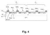
図3、4にセンサの構造の断面図を示す。図3は、図2の線III−IIIに沿って狭いフィンガー部20を切った断面図である。図4は、図2の線IV−IVに沿った横断面であるが、ゲートとフォトダイオードの間にはフィンガー部がなくp+領域18だけがある。
3 and 4 are sectional views of the sensor structure. FIG. 3 is a cross-sectional view of the
ピクセルは、上部が能動型で低濃度の不純物が添加されたエピタキシャル半導体層12である半導体基板10に形成されている。本例では、基板は高濃度不純物が添加されたp++型であり、能動エピタキシャル層はp−型である。エピタキシャル層がn型であれば、フォトダイオードおよびゲートに印加された電位の符号と合わせて、全ての種類の導電性を反転させる必要があろう。基板は原理的にエピタキシャル層と同種の導電性を有しているが、逆の種類であってもよい。
The pixel is formed on a
ゲートは多結晶シリコンゲートであって、薄い絶縁層13(シリコン酸化物または窒化物)によりエピタキシャル層12から絶縁されている。フォトダイオードは「ピン止め」フォトダイオードであり、すなわち、p型のエピタキシャル層12(全てのピクセルの全てのフォトダイオードに共通の能動層)、2個の転送ゲート間のエピタキシャル層に拡散されてn型の個別領域14、およびエピタキシャル層よりも高濃度に不純物が添加されていて個別領域14を覆い、固定電位に保持されたp型の表面個別領域16を含む多層フィルムにより形成されている。照射により生成された電子は、n領域とエピタキシャルp層の間の接合部に形成された電位井戸に蓄積可能である。
The gate is a polycrystalline silicon gate and is insulated from the
図4のみに示すP+型不純物が添加された領域18は、表面領域16よりも高濃度に不純物が添加されている。当該領域には、能動層12の電位である基準低電位が印加されている。当該領域は表面領域に隣接し、表面領域の電位を当該電位に合わせる。
The
青色における感度の向上に望ましいように表面領域16が極めて浅い場合、領域18は好適には領域16よりも深い。
ピクセル列は、異なる列のピクセル間での電荷転送を一切阻止する絶縁域STI(シリコン酸化物または他の絶縁体)により分離されている。 The pixel columns are separated by an isolation region STI (silicon oxide or other insulator) that prevents any charge transfer between pixels in different columns.
図5に、能動層内で、電荷の保存および転送が行われる深さ、すなわち能動層の最上面の僅かに下側の電位の線図を示す。 FIG. 5 shows a diagram of the depth at which charge is stored and transferred in the active layer, ie, the potential slightly below the top surface of the active layer.
動作の様々な段階における電位を示しており、ゲートに適用された所与の電位について、狭いフィンガー部の下側で電位が、フィンガー部が狭いことに効果的に起因して、ゲートの残りの部分の下側の電位とは同一ではないことを考慮している。より正確には、ゲートに印加され、従った当該ゲートの狭いフィンガー部に印加された所与の電位について、狭いフィンガー部を囲むp+領域18の低電位により生じた影響は、ゲートの残りの部分の下側における半導体の電位に対して狭いフィンガー部の下側における半導体の電位を減少させる傾向があるが、p+領域における程には減少させない。通常の慣例に従えば、増大しつつある電位は、電子の電位井戸および電位障壁を明確にすべく下方へ導かれる。 The potential at various stages of operation is shown, and for a given potential applied to the gate, the potential below the narrow finger is effectively due to the narrow finger, and the rest of the gate It is considered that the lower potential of the part is not the same. More precisely, for a given potential applied to the narrow finger portion of the gate, and thus to the narrow finger portion of the gate, the effect caused by the low potential of the p + region 18 surrounding the narrow finger portion is the rest of the gate. There is a tendency to decrease the semiconductor potential below the narrow finger portion relative to the semiconductor potential below the portion, but not as much as in the p + region. In accordance with normal practice, the increasing potential is directed downward to clarify the potential well and potential barrier of the electrons.
例示する電位線図は、図2の切断線V−Vに沿った電位の変動に対応しており、切断線V−Vは分かり易くするために当該線図より上に示す。 The illustrated potential diagram corresponds to the fluctuation of the potential along the cutting line VV in FIG. 2, and the cutting line VV is shown above the diagram for easy understanding.
2個の動作モード、すなわち
− 積分周期にわたり電荷がゲートの下側に蓄積されるモードであって、この場合、第1の積分半周期にわたり高電位が列方向(電荷の転送方向)のゲートに一つ置きに印加され、当該高電位が対象ゲートの下側に電位井戸を生成し、他のゲートは低電位を受け取り、第1の積分半周期の終了時点でゲートの役割が入れ替わり、高電位のゲートが低電位を受け取り、その逆も生じ、自身の狭いフィンガー部を上流に向けられたゲートだけが当該シーケンスの対象となり、他のゲートは固定された低電位を受け取るが、電荷を受け取ることも電荷を通過させることもできないモードと、
− 積分周期にわたり電荷がゲートの下側ではなくフォトダイオード内に蓄積され、ゲートは短時間の転送動作中に電荷を一時的に保存するだけであるモードとが可能である。
Two modes of operation: a mode in which charge is accumulated below the gate over the integration period, where a high potential is applied to the gate in the column direction (charge transfer direction) over the first integration half period. Applied every other time, the high potential generates a potential well below the target gate, the other gates receive a low potential, and the role of the gate is switched at the end of the first integration half-cycle, resulting in a high potential. One gate receives a low potential, and vice versa, only the gate with its narrow finger pointed upstream is subject to the sequence, the other gates receive a fixed low potential but receive a charge Mode that can not pass the charge,
A mode is possible in which charge is stored in the photodiode rather than under the gate over the integration period, and the gate only temporarily stores the charge during a short transfer operation.
図5は第2のモードに対応し、かつ2段階の動作に対応しており、すなわち略正方形の形状をなす各ピクセルが2個のフォトダイオードを含み、積分周期が2個の積分半周期に分割されて各半周期の後で電荷が部分的に転送されることを意味する。センサが、ピクセルが3または4個のフォトダイオードを含む略正方形の形状をなす状態で、3または4段階で動作することを想起されたい。 FIG. 5 corresponds to the second mode and corresponds to a two-step operation, that is, each pixel having a substantially square shape includes two photodiodes, and the integration period is two integration half periods. It means that the charge is partially transferred after each half cycle. Recall that the sensor operates in 3 or 4 stages, with the pixel in the shape of a substantially square containing 3 or 4 photodiodes.
図5は、図2の最上部から最下部への電荷転送に対応しており、すなわち右側ゲートG1B、G2Bが当該ゲートを通して転送を行うべく能動的に使用され、左側ゲートG1A、G2Aは中性化されている。 FIG. 5 corresponds to charge transfer from the top to the bottom of FIG. 2, that is, the right gates G1B and G2B are actively used to transfer through the gates, and the left gates G1A and G2A are neutral. It has become.
線図の各ステップに対して、能動チャネルの電位Vactを示しており、中性化された電位Vneut(時間経過と共に変化しないが、中性化されたゲートの下側で電荷の通過を禁止する役割を果たす)も示している。 For each step of the diagram, the potential V act of the active channel is shown, and the neutralized potential V neut (which does not change over time, but does not pass charge underneath the neutralized gate. It also shows the role of prohibition).
全ての中性化されたゲートG1A、G2Aは、全ての積分および電荷転送周期にわたり低電位に留まっている。当該ゲートの下側では電荷の蓄積または転送は一切生じ得ない。 All neutralized gates G1A, G2A remain at a low potential for all integration and charge transfer periods. No charge accumulation or transfer can occur below the gate.
電荷が存在しないと思われるフォトダイオード内の半導体の電位は、p型の表面層が能動層の基準電位に保持されている事実により固定値を有する。空のフォトダイオードの基本電位を破線で示す。基本電位はフォトダイオード内の領域12、14、16の不純物添加の度合に依存する。
The potential of the semiconductor in the photodiode where no charge appears to be present has a fixed value due to the fact that the p-type surface layer is held at the reference potential of the active layer. The basic potential of the empty photodiode is indicated by a broken line. The basic potential depends on the degree of impurity addition in the
電位は、持続期間が各々Tint/2である2段階に分割された1個の積分周期Tintにわたり変動する。 The potential fluctuates over one integration period T int divided into two stages each having a duration of T int / 2.
図5の線図の第1の2行のグループは、初期時点0から時点Tint/2までの第1の積分半周期にわたる能動層の内部電位を表す。全てのゲートG1B、G2Bは低電位にあり(ゲートG1A、G2Aと同様)、電荷は全てのフォトダイオードの下側に形成された電位井戸内の光の影響下で段階的に蓄積される。当該井戸は、能動ゲートおよび中性化されたゲートに印加された低電位により閉じられる。これらはまた、ゲートの下側に形成された障壁よりも高い電位障壁を形成するp+領域18により閉じられる。最後に、これらはまた、ピクセルの列を互いに分離する絶縁領域STIによっても閉じられる。 The first two rows of groups in the diagram of FIG. 5 represent the internal potential of the active layer over a first integration half-cycle from initial time 0 to time T int / 2. All the gates G1B and G2B are at a low potential (similar to the gates G1A and G2A), and charges are accumulated stepwise under the influence of light in a potential well formed below all photodiodes. The well is closed by a low potential applied to the active gate and the neutralized gate. They are also closed by a p + region 18 that forms a higher potential barrier than the barrier formed below the gate. Finally, they are also closed by insulating regions STI that separate the columns of pixels from one another.
線図の第2の行のグループは、時点Tint/2−ε、すなわち第1の積分半周期Tint/2の終了直前における内部電位を表す。フォトダイオードは、当該期間にわたる照射により生成された全ての電荷を取得している。 The group in the second row of the diagram represents the internal potential just before the end of the time T int / 2−ε, ie the first integration half cycle T int / 2. The photodiode acquires all the charges generated by irradiation over the period.
第3の行のグループは、短い転送パルスを能動ゲートに一つ置きに印加した時点を表す。ここで、ゲートG1B(G1Bi、G1Bi+1、等)は全て当該転送パルスを受け取るが、ゲートG2B(G2Bi、G2Bi+1)は受け取らない。
The third group of rows represents the instant at which every other short transfer pulse is applied to the active gate. Here, the
転送パルスは、自身を受け取るゲートの下側で電位井戸を形成している高電位にある。フォトダイオードに隣接するゲートの下側で当該フォトダイオードに蓄積された電荷は当該ゲートに保存される。これは、ゲートG1BiがフォトダイオードPH1iから電荷を受け取るだけでなく、すく上流に配置されたピクセルのフォトダイオードPH2i−1からも(自身の狭いフィンガー部を通して)電荷を受け取ることを意味する。同様に、ゲートG1Bi+1はフォトダイオードPH2iから電荷を受け取ると共に、すぐ下流に配置されたピクセルのフォトダイオードPH1i+1からも電荷を受け取る。 The transfer pulse is at a high potential forming a potential well below the gate receiving it. The charge accumulated in the photodiode below the gate adjacent to the photodiode is stored in the gate. This means that the gate G1B i not only receives charge from the photodiode PH1 i , but also receives (through its narrow fingers) the pixel photodiode PH2 i-1 located immediately upstream. . Similarly, the gate G1B i + 1 receives the charge from the photodiode PH2 i and also receives the charge from the photodiode PH1 i + 1 of the pixel arranged immediately downstream.
第4の行のグループは、時点Tint+ε、すなわち短い転送パルスの終了直後における電位の状態を表す。ゲートG1Bの下側の電位は最初の低レベルに戻る。ゲートG1Bの下側に保存された電荷は、下流側の隣接フォトダイオードへ放出される。当該電荷は、狭いフィンガー部(p+領域18が障壁を形成している)の下側しか通過できないため、上流のフォトダイオードに向かって行かないが、狭いフィンガー部の下側の電位はゲートの下側の残りの電位よりも低く、電荷は自然に下流方向に向けられる。従って、フォトダイオードPH1(PH1i、PH1i+1)だけが電荷を受け取り、フォトダイオードPH2には電荷が無い状態が続く。 The group in the fourth row represents the state of the potential at the instant T int + ε, ie immediately after the end of the short transfer pulse. The potential on the lower side of the gate G1B returns to the initial low level. The charge stored under the gate G1B is discharged to the adjacent photodiode on the downstream side. Since the charge can only pass under the narrow finger (p + region 18 forms a barrier), it does not go to the upstream photodiode, but the potential under the narrow finger is Below the remaining potential on the lower side, the charge is naturally directed in the downstream direction. Therefore, only the photodiode PH1 (PH1 i , PH1 i + 1 ) receives charges, and the photodiode PH2 continues to have no charge.
第5の行のグループは、新たな転送パルスの直前の時点Tint−εにおける第2の積分半周期の終了を表す。フォトダイオードPH2iは、第2の積分半周期にわたり当該フォトダイオードを照射した結果生じた電荷で満たされているが、フォトダイオードPH1iは同時に、当該半周期にわたりピクセルを照射した結果生じた電荷およびフォトダイオードPH1i、PH2i−1から発せられた先行転送パルスの持続期間中に転送された電荷で満たされている。 The fifth row group represents the end of the second integration half-cycle at a time T int -ε immediately before the new transfer pulse. The photodiode PH2 i is filled with the charge resulting from irradiating the photodiode over the second integration half-cycle, while the photodiode PH1 i is simultaneously charged as a result of irradiating the pixel over the half-cycle and It is filled with the charge transferred during the duration of the preceding transfer pulse emitted from the photodiodes PH1 i and PH2 i-1 .
第6の行のグループは、時点Tintにおける第2の短い転送パルスの持続期間中の電位の状態を表す。ゲートG2Bの電位は、当該ゲートの下側に電位井戸を形成すべく高レベルに上げられている。ゲートG1Bの電位は変化しない。ゲートG2Biに隣接するフォトダイオードPH1i、PH2iからの電荷は、ゲートG2Biの下側を移動する。 The sixth group of rows, representing the state of the potential of the duration of the second short transfer pulse at time T int. The potential of the gate G2B is raised to a high level to form a potential well below the gate. The potential of the gate G1B does not change. Charge from the photodiode PH1 i, PH2 i adjacent to the gate G2B i moves the lower gate G2B i.
最後に、第7の行のグループは、時点Tint+εにおける、すなわち短い転送パルスの終了時点における電位の最終状態を表す。ゲートG2Bの電位は、低い状態に戻されている。電荷はフォトダイオードへ戻るが、電位障壁が狭いフィンガー部の下側で高く、ゲートの残りの部分の下側で低いため、上流から下流への一方向だけに移動する。フォトダイオードPH2は、ゲートG2Bの下側に一時的に保存された電荷で満たされている。フォトダイオードPH1には電荷が無い状態が続く。 Finally, the seventh row group represents the final state of the potential at time T int + ε, ie at the end of the short transfer pulse. The potential of the gate G2B is returned to the low state. The charge returns to the photodiode, but moves only in one direction from upstream to downstream because the potential barrier is high below the narrow finger and low below the rest of the gate. The photodiode PH2 is filled with the electric charge temporarily stored below the gate G2B. The photodiode PH1 continues to have no charge.
当該最終状態態は、新たな積分周期の初期状態となる。フォトダイオードPH2iに含まれる電荷は、(時点0で)フォトダイオードPH2i−1に既に含まれていた電荷、第1の積分半周期にわたりフォトダイオードPH2i−1、PH1iにより生成された電荷、および第2の積分半周期にわたりフォトダイオードPH1i、PH2iにより生成された電荷の合算である。フォトダイオードPH1(PH1i、PH1i+1)には当該初期状態の電荷が無い。 The final state is an initial state of a new integration cycle. The charge contained in the photodiode PH2 i is the charge already contained in the photodiode PH2 i-1 (at time 0), the charge generated by the photodiodes PH2 i-1 and PH1 i over the first integration half cycle. , And the charge generated by the photodiodes PH1 i , PH2 i over the second integration half-cycle. The photodiode PH1 (PH1 i , PH1 i + 1 ) has no charge in the initial state.
電荷転送の全体的な方向は左から右に向かうものであり、すなわち、積分周期Tintの開始時点で上流にあるピクセルの第2のフォトダイオードPH2i−1に蓄積されていた電荷が、周期Tintにわたり生成された電荷と共に、後続する積分周期の開始時点で次のピクセルの第2のフォトダイオードPH2iに存在することになる。従って、電荷の右向き一方向の転送および、先行ピクセルに蓄積された電荷と現在のピクセル内で生成された電荷との合算の両方が生じ、これら全てがTDI型の動作を生じさせる。 The overall direction of charge transfer is from left to right, that is, the charge accumulated in the second photodiode PH2 i-1 of the upstream pixel at the start of the integration period T int is the period. with charge generated over T int, it will be present in the second photodiode PH2 i for the next pixel at the beginning of the subsequent integration period. Thus, there is both a rightward transfer of charge and a summation of the charge accumulated in the previous pixel and the charge generated in the current pixel, all of which give rise to a TDI type operation.
ゲートGA、GBの役割を入れ替え、かつ信号の同一時間順序を保存することにより、転送方向が反転される。 By changing the roles of the gates GA and GB and preserving the same time order of signals, the transfer direction is reversed.
シミュレーションの実行により、電位障壁BP1i、BP2iの高さが狭いフィンガー部20の幅に合わせて大幅に変動することが示される。典型的には、フィンガー部の幅が0.7マイクロメートル〜0.1マイクロメートルの範囲で変動するのに伴い0.5ボルト〜2.5ボルトの範囲で変動し得る。当該値は、使用するエッチング技術および注入のレベルに依存するため例示的に過ぎない。フィンガー部の幅が0.4マイクロメートル以下であることが良好な選択である。転送方向でのフィンガー部の長さは約0.4マイクロメートルであってよい。
By executing the simulation, it is shown that the height of the potential barriers BP1 i and BP2 i varies greatly according to the width of the
同一ゲートのフィンガー部の終端がゲートの狭い細片により互いに接続可能である点に注意されたい。 Note that the ends of the fingers of the same gate can be connected to each other by narrow strips of the gate.
電荷は、ある列の終端で、好適には一連の電荷蓄積ノードおよび電荷電圧変換回路(1個の電荷蓄積ノードおよび1個の電荷電圧変換回路がマトリクスの各列に関連付けられている)に放出される。変換回路は、CMOS技術を利用したセンサ能動ピクセルのトランジスタと同様の数個のトランジスタを含み、その中にフォロワトランジスタおよびリセットトランジスタがある。次いで、変換回路は好適には、最初に電荷蓄積ノードの電位がリセットされた時点のリセット電位レベルを、次いでマトリクスの最終行から電荷蓄積ノードへ電荷を放出した後で有用な信号のレベルをサンプリングする相関二重サンプリング回路に関連付けられる。2個のサンプルの差異はA/Dコンバータにより変換される。ピクセルの各列に簡便なコンバータが設けられていてよく、そうでない場合には大域的コンバータが各々の列の変換を順次実行する。 Charge is discharged at the end of a column, preferably to a series of charge storage nodes and charge voltage conversion circuits (one charge storage node and one charge voltage conversion circuit associated with each column of the matrix). Is done. The conversion circuit includes several transistors similar to those of sensor active pixels using CMOS technology, among which are a follower transistor and a reset transistor. The conversion circuit then preferably samples the reset potential level when the charge storage node potential is first reset, and then the useful signal level after discharging the charge from the last row of the matrix to the charge storage node. Associated with a correlated double sampling circuit. The difference between the two samples is converted by an A / D converter. A simple converter may be provided for each column of pixels, otherwise the global converter performs the conversion of each column sequentially.
図6に、ゲートの一変形実施形態を示す。ピクセルに関連付けられていてゲートの同一行の一部を形成する2個のゲートのうち、一方のゲート(G1B)が図示しない導体により互いに電気的に接続された2個の部分に分割され、当該2個の部分が他方のゲート(G1A)の両側に配置さえている。 FIG. 6 shows a modified embodiment of the gate. Of the two gates associated with the pixel and forming part of the same row of gates, one gate (G1B) is divided into two parts electrically connected to each other by a conductor not shown, Two parts are even arranged on both sides of the other gate (G1A).
図7に、2個のゲートG1A、G1Bが少なくとも2個の部分に分割され、一方のゲートの一部が他方のゲートの一部に幾何学的に交互に配置された別の変形例を示す。各部は、ゲートGAの一部であるかゲートGBの一部であるかに応じて、フォトダイオードのどちらかに向けられた少なくとも1個の狭いフィンガー部を含んでいる。 FIG. 7 shows another modification in which two gates G1A and G1B are divided into at least two parts, and a part of one gate is geometrically arranged alternately on a part of the other gate. . Each part includes at least one narrow finger directed to either of the photodiodes depending on whether it is part of the gate GA or part of the gate GB.
ゲートの構成の如何に依らず、ゲート(ゲートは透明である)の下側の半導体に生成された電子が、ゲートに隣接するフォトダイオードのどちらかへ事前に誘導されるという事実により、幾何学的変調伝達関数が劣化するリスクが存在する。上記リスクがMTFに悪影響を及ぼすか及ぼさないかは、上記捕捉が積分半周期のどちらで生じるかに依存する。 Regardless of the configuration of the gate, due to the fact that electrons generated in the semiconductor under the gate (the gate is transparent) are pre-directed to either photodiode adjacent to the gate, the geometry There is a risk that the dynamic modulation transfer function will degrade. Whether the risk adversely affects the MTF depends on whether the acquisition occurs during the integration half-cycle.
従って、例えば、
− 第2の積分半周期にわたりゲートG2Biの下側に生成された電子は通常、フォトダイオードPHi2の方へ誘導され、これに続く転送パルスの持続期間中、ゲートG2Biの方へ、次いでフォトダイオードPH2iの方へ誘導され、
− 同一時点でゲートG2Aiの下側に生成された電子は通常、フォトダイオードPH1iの方へ誘導され、これに続く転送パルスの持続期間中、ゲートG2Biの方へ、次いでフォトダイオードPH2iの方へも誘導される。
So, for example,
-The electrons generated under the gate G2B i over the second integration half-cycle are usually directed towards the photodiode PHi 2 and then towards the gate G2B i for the duration of the subsequent transfer pulse, then Guided to the photodiode PH2 i ,
- The electrons generated below the gate G2A i at the same time usually induced toward the photodiode PH1 i, the duration of the transfer pulse followed by, towards the gate G2B i, then photodiode PH2 i It is also guided towards.
この場合、電子がゲートG2AiまたはゲートG2Biのいずれの下側に生成されたかに依らず、電子の扱いに違いはなく、これは有利である。 In this case, there is no difference in the handling of the electrons, which is advantageous regardless of whether the electrons are generated below the gate G2A i or the gate G2B i .
しかし、
− 第1の積分半周期にわたりゲートG2Biの下側に生成された電子は通常、フォトダイオードPHi2の方へ誘導され、これに続く転送パルスの持続期間中、ゲートG1Bi+1の方へ、次いでフォトダイオードPH1i+1の方へ誘導され、
− 反対に、同一時点でゲートG2Aiの下側に生成された電子は通常、フォトダイオードPH1iの方へ誘導され、これに続く転送パルスの持続期間中、ゲートG1Biの方へ、次いでフォトダイオードPH1iの方へ逆向きに移動する。
But,
-The electrons generated under the gate G2B i over the first integration half-cycle are usually directed towards the photodiode PHi 2 and then towards the gate G1B i + 1 for the duration of the subsequent transfer pulse, then Guided towards the photodiode PH1 i + 1 ,
- Conversely, electrons generated below the gate G2A i at the same time usually for the duration of the induced towards the photodiode PH1 i, transfer pulse followed by, towards the gate G1B i, then the photo It moves in the opposite direction towards the diode PH1 i .
従って、電子がゲートG2Biの下側またはゲートG2Aiの下側に生成されたかに依存して扱いに違いがある。この違いは、あるピクセルから到達した電子と別のピクセルから到達した電子を混合することで変調伝達関数に悪影響を及ぼす。 Therefore, electrons there are differences in treatment depending on whether generated on the lower side of the lower or gate G2A i gate G2B i. This difference adversely affects the modulation transfer function by mixing electrons arriving from one pixel with electrons arriving from another pixel.
この劣化を回避すべく提供される解決策は、各々の半ピクセルを、半ピクセルの表面の最上部で受光した光をフォトダイオード上に集光する集光マイクロレンズで覆うものである。従って、電子はゲートの下側ではなくフォトダイオード内で系統的に生成される。 A solution provided to avoid this degradation is to cover each half-pixel with a condensing microlens that collects the light received at the top of the half-pixel surface onto a photodiode. Thus, electrons are systematically generated in the photodiode rather than under the gate.
図8の実施形態において、マイクロレンズMLは矩形の形状を有し、フォトダイオードの中心に配置されている。マイクロレンズMLは、フォトダイオードの両側に配置されたゲートの表面の半分と共に、フォトダイオード全体を覆う。2個の個別の半ピクセルを覆う2個の隣接するマイクロレンズが、ピクセル全体に対応する略正方形の形状を覆う。 In the embodiment of FIG. 8, the microlens ML has a rectangular shape and is arranged at the center of the photodiode. The microlens ML covers the entire photodiode together with half of the surface of the gate disposed on both sides of the photodiode. Two adjacent microlenses covering two individual half-pixels cover a substantially square shape corresponding to the entire pixel.
図9の実施形態における解決策は、矩形のマイクロレンズの代わりに、2個の隣接する正方形のマイクロレンズを行MLa、MLbに設けるものである。各マイクロレンズは、フォトダイオードの半分の中心に配置され、フォトダイオードの当該半分およびフォトダイオードの当該半分に隣接するゲートの半分を覆う。4個の隣接する正方形のマイクロレンズがピクセル全体に対応する略正方形の表面を覆う。 The solution in the embodiment of FIG. 9 is to provide two adjacent square microlenses in rows MLa and MLb instead of rectangular microlenses. Each microlens is placed in the center of the half of the photodiode and covers the half of the photodiode and the half of the gate adjacent to the half of the photodiode. Four adjacent square microlenses cover a substantially square surface corresponding to the entire pixel.
Claims (9)
Applications Claiming Priority (3)
| Application Number | Priority Date | Filing Date | Title |
|---|---|---|---|
| FR1254070A FR2990299B1 (en) | 2012-05-03 | 2012-05-03 | MATRIX IMAGE SENSOR WITH TWO-WAY CHARGING TRANSFER WITH DISSYMETRIC GRIDS |
| FR1254070 | 2012-05-03 | ||
| PCT/EP2013/057546 WO2013164169A1 (en) | 2012-05-03 | 2013-04-11 | Matrix image sensor providing bidirectional charge transfer with asymmetric gates |
Publications (3)
| Publication Number | Publication Date |
|---|---|
| JP2015524159A JP2015524159A (en) | 2015-08-20 |
| JP2015524159A5 JP2015524159A5 (en) | 2016-05-19 |
| JP6133973B2 true JP6133973B2 (en) | 2017-05-24 |
Family
ID=46754595
Family Applications (1)
| Application Number | Title | Priority Date | Filing Date |
|---|---|---|---|
| JP2015509353A Expired - Fee Related JP6133973B2 (en) | 2012-05-03 | 2013-04-11 | Matrix image sensor with bi-directional charge transfer with asymmetric gate |
Country Status (9)
| Country | Link |
|---|---|
| US (1) | US9093353B2 (en) |
| EP (1) | EP2845231B1 (en) |
| JP (1) | JP6133973B2 (en) |
| KR (1) | KR102105730B1 (en) |
| CN (1) | CN104303306B (en) |
| FR (1) | FR2990299B1 (en) |
| IL (1) | IL235437B (en) |
| IN (1) | IN2014DN08844A (en) |
| WO (1) | WO2013164169A1 (en) |
Families Citing this family (1)
| Publication number | Priority date | Publication date | Assignee | Title |
|---|---|---|---|---|
| CN114122141A (en) * | 2016-03-23 | 2022-03-01 | 派赛公司 | Semiconductor structure and method for providing body tie to cascode transistor |
Family Cites Families (20)
| Publication number | Priority date | Publication date | Assignee | Title |
|---|---|---|---|---|
| JP3474638B2 (en) * | 1994-06-30 | 2003-12-08 | 株式会社東芝 | Solid-state imaging device |
| US6906749B1 (en) | 1998-09-16 | 2005-06-14 | Dalsa, Inc. | CMOS TDI image sensor |
| US6465820B1 (en) * | 1998-09-16 | 2002-10-15 | Dalsa, Inc. | CMOS compatible single phase CCD charge transfer device |
| US6633058B1 (en) * | 1999-07-26 | 2003-10-14 | Dalsa, Inc. | Variable reticulation time delay and integrate sensor |
| KR100434806B1 (en) | 1999-10-05 | 2004-06-07 | 캘리포니아 인스티튜트 오브 테크놀로지 | Time-delayed-integration imaging with active pixel sensors |
| US20020097330A1 (en) * | 2001-01-25 | 2002-07-25 | Spears Kurt E. | Photosensor array using segmented charge transfer gates to improve processing time for small images |
| US8446508B2 (en) * | 2005-07-27 | 2013-05-21 | Sony Corporation | Solid state imaging device with optimized locations of internal electrical components |
| FR2906080B1 (en) | 2006-09-19 | 2008-11-28 | E2V Semiconductors Soc Par Act | SCALING IMAGE SENSOR WITH SUCCESSIVE INTEGRATIONS AND SOMMATION, WITH ACTIVE CMOS PIXELS |
| US7923763B2 (en) | 2007-03-08 | 2011-04-12 | Teledyne Licensing, Llc | Two-dimensional time delay integration visible CMOS image sensor |
| JP2009033286A (en) * | 2007-07-25 | 2009-02-12 | Advanced Mask Inspection Technology Kk | Storage type sensor and driving method thereof |
| FR2924532B1 (en) * | 2007-11-30 | 2009-12-18 | E2V Semiconductors | PIXEL FOUR OR FIVE TRANSISTOR IMAGE SENSOR WITH REDUCTION OF RESET NOISE |
| JP5300577B2 (en) * | 2009-04-23 | 2013-09-25 | 三菱電機株式会社 | TDI image sensor and method for driving the image sensor |
| KR101621278B1 (en) * | 2009-07-27 | 2016-05-17 | 삼성전자주식회사 | Photo detecting apparatus and unit pixel thereof |
| JP5568934B2 (en) * | 2009-09-29 | 2014-08-13 | ソニー株式会社 | Solid-state imaging device, method for manufacturing solid-state imaging device, electronic device, lens array |
| FR2953642B1 (en) * | 2009-12-09 | 2012-07-13 | E2V Semiconductors | MULTILINEAIRE IMAGE SENSOR WITH CHARGE INTEGRATION. |
| JP5509846B2 (en) * | 2009-12-28 | 2014-06-04 | ソニー株式会社 | SOLID-STATE IMAGING DEVICE, ITS MANUFACTURING METHOD, AND ELECTRONIC DEVICE |
| FR2959902B1 (en) * | 2010-05-04 | 2013-08-23 | E2V Semiconductors | LINEAR IMAGE SENSOR WITH SCROLL AND ANALOG AND DIGITAL SUMMIT AND METHOD THEREOF |
| FR2960341B1 (en) * | 2010-05-18 | 2012-05-11 | E2V Semiconductors | MATRIX IMAGE SENSOR WITH TRANSFER OF DISSYMETRIC GRID LOADS. |
| FR2961347B1 (en) * | 2010-06-15 | 2012-08-24 | E2V Semiconductors | ELECTRON MULTIPLICATION IMAGE SENSOR |
| FR2973162B1 (en) * | 2011-03-23 | 2013-11-22 | E2V Semiconductors | VERY HIGH DYNAMIC IMAGE SENSOR |
-
2012
- 2012-05-03 FR FR1254070A patent/FR2990299B1/en not_active Expired - Fee Related
-
2013
- 2013-04-11 EP EP13714967.0A patent/EP2845231B1/en not_active Not-in-force
- 2013-04-11 US US14/397,725 patent/US9093353B2/en not_active Expired - Fee Related
- 2013-04-11 KR KR1020147029985A patent/KR102105730B1/en active IP Right Grant
- 2013-04-11 WO PCT/EP2013/057546 patent/WO2013164169A1/en active Application Filing
- 2013-04-11 CN CN201380023055.8A patent/CN104303306B/en not_active Expired - Fee Related
- 2013-04-11 JP JP2015509353A patent/JP6133973B2/en not_active Expired - Fee Related
-
2014
- 2014-10-21 IN IN8844DEN2014 patent/IN2014DN08844A/en unknown
- 2014-11-02 IL IL235437A patent/IL235437B/en active IP Right Grant
Also Published As
| Publication number | Publication date |
|---|---|
| IL235437B (en) | 2019-05-30 |
| IL235437A0 (en) | 2014-12-31 |
| KR102105730B1 (en) | 2020-04-28 |
| FR2990299B1 (en) | 2014-05-09 |
| KR20150017698A (en) | 2015-02-17 |
| CN104303306A (en) | 2015-01-21 |
| CN104303306B (en) | 2017-04-12 |
| IN2014DN08844A (en) | 2015-05-22 |
| US20150123174A1 (en) | 2015-05-07 |
| EP2845231B1 (en) | 2016-04-06 |
| US9093353B2 (en) | 2015-07-28 |
| FR2990299A1 (en) | 2013-11-08 |
| EP2845231A1 (en) | 2015-03-11 |
| WO2013164169A1 (en) | 2013-11-07 |
| JP2015524159A (en) | 2015-08-20 |
Similar Documents
| Publication | Publication Date | Title |
|---|---|---|
| US9865632B2 (en) | Image sensor pixel with memory node having buried channel and diode portions formed on N-type substrate | |
| JP6044044B2 (en) | Asymmetric gate matrix charge transfer image sensor | |
| US7642499B2 (en) | Image sensor comprising multilayer wire | |
| US9040890B2 (en) | Electron-multiplication image sensor | |
| JPS62265759A (en) | Solid state image pickup element | |
| KR101788890B1 (en) | Charge-integration multilinear image sensor | |
| US8497546B2 (en) | Back-side-illuminated image sensors with bulk-charge-modulated image sensor pixels | |
| KR101968340B1 (en) | Charge-integration multilinear image sensor | |
| US3995302A (en) | Transfer gate-less photosensor configuration | |
| EP0473765A1 (en) | Image sensor. | |
| US5703642A (en) | Full depletion mode clocking of solid-state image sensors for improved MTF performance | |
| JP6133973B2 (en) | Matrix image sensor with bi-directional charge transfer with asymmetric gate | |
| JP2020080377A (en) | Solid-state imaging device | |
| TWI711167B (en) | Charge transfer image sensor with double gate implantation | |
| US20160255295A1 (en) | Image sensor with electron multiplication and grouped readout of pixels | |
| EP3719842A1 (en) | 4t pixel and image sensor comprising the same |
Legal Events
| Date | Code | Title | Description |
|---|---|---|---|
| A521 | Request for written amendment filed |
Free format text: JAPANESE INTERMEDIATE CODE: A523 Effective date: 20160325 |
|
| A621 | Written request for application examination |
Free format text: JAPANESE INTERMEDIATE CODE: A621 Effective date: 20160325 |
|
| A977 | Report on retrieval |
Free format text: JAPANESE INTERMEDIATE CODE: A971007 Effective date: 20170120 |
|
| A131 | Notification of reasons for refusal |
Free format text: JAPANESE INTERMEDIATE CODE: A131 Effective date: 20170131 |
|
| A521 | Request for written amendment filed |
Free format text: JAPANESE INTERMEDIATE CODE: A523 Effective date: 20170223 |
|
| TRDD | Decision of grant or rejection written | ||
| A01 | Written decision to grant a patent or to grant a registration (utility model) |
Free format text: JAPANESE INTERMEDIATE CODE: A01 Effective date: 20170328 |
|
| A61 | First payment of annual fees (during grant procedure) |
Free format text: JAPANESE INTERMEDIATE CODE: A61 Effective date: 20170420 |
|
| R150 | Certificate of patent or registration of utility model |
Ref document number: 6133973 Country of ref document: JP Free format text: JAPANESE INTERMEDIATE CODE: R150 |
|
| S533 | Written request for registration of change of name |
Free format text: JAPANESE INTERMEDIATE CODE: R313533 |
|
| R350 | Written notification of registration of transfer |
Free format text: JAPANESE INTERMEDIATE CODE: R350 |
|
| R250 | Receipt of annual fees |
Free format text: JAPANESE INTERMEDIATE CODE: R250 |
|
| LAPS | Cancellation because of no payment of annual fees |