JP6127561B2 - Semiconductor photo detector - Google Patents
Semiconductor photo detector Download PDFInfo
- Publication number
- JP6127561B2 JP6127561B2 JP2013025660A JP2013025660A JP6127561B2 JP 6127561 B2 JP6127561 B2 JP 6127561B2 JP 2013025660 A JP2013025660 A JP 2013025660A JP 2013025660 A JP2013025660 A JP 2013025660A JP 6127561 B2 JP6127561 B2 JP 6127561B2
- Authority
- JP
- Japan
- Prior art keywords
- submount
- header
- electrode pad
- semiconductor light
- light receiving
- Prior art date
- Legal status (The legal status is an assumption and is not a legal conclusion. Google has not performed a legal analysis and makes no representation as to the accuracy of the status listed.)
- Active
Links
- 239000004065 semiconductor Substances 0.000 title claims description 73
- BQCADISMDOOEFD-UHFFFAOYSA-N Silver Chemical compound [Ag] BQCADISMDOOEFD-UHFFFAOYSA-N 0.000 claims description 12
- 229910052709 silver Inorganic materials 0.000 claims description 12
- 239000004332 silver Substances 0.000 claims description 12
- 239000003990 capacitor Substances 0.000 claims description 11
- 239000004020 conductor Substances 0.000 claims description 6
- PCHJSUWPFVWCPO-UHFFFAOYSA-N gold Chemical group [Au] PCHJSUWPFVWCPO-UHFFFAOYSA-N 0.000 claims description 4
- 239000010931 gold Substances 0.000 claims description 4
- 229910052737 gold Inorganic materials 0.000 claims description 4
- 239000011347 resin Substances 0.000 claims description 4
- 229920005989 resin Polymers 0.000 claims description 4
- 239000003989 dielectric material Substances 0.000 claims description 3
- 230000002093 peripheral effect Effects 0.000 claims description 3
- 239000011230 binding agent Substances 0.000 claims description 2
- 230000004048 modification Effects 0.000 description 21
- 238000012986 modification Methods 0.000 description 21
- 238000005520 cutting process Methods 0.000 description 7
- 238000010586 diagram Methods 0.000 description 7
- 230000000052 comparative effect Effects 0.000 description 6
- 230000008901 benefit Effects 0.000 description 3
- 239000011521 glass Substances 0.000 description 3
- 229910052751 metal Inorganic materials 0.000 description 3
- 239000002184 metal Substances 0.000 description 3
- IJGRMHOSHXDMSA-UHFFFAOYSA-N Atomic nitrogen Chemical compound N#N IJGRMHOSHXDMSA-UHFFFAOYSA-N 0.000 description 2
- XEEYBQQBJWHFJM-UHFFFAOYSA-N Iron Chemical compound [Fe] XEEYBQQBJWHFJM-UHFFFAOYSA-N 0.000 description 2
- 230000002411 adverse Effects 0.000 description 2
- 230000000694 effects Effects 0.000 description 2
- 239000007789 gas Substances 0.000 description 2
- 238000007747 plating Methods 0.000 description 2
- 239000000853 adhesive Substances 0.000 description 1
- 230000001070 adhesive effect Effects 0.000 description 1
- 238000005452 bending Methods 0.000 description 1
- 239000000919 ceramic Substances 0.000 description 1
- 238000007796 conventional method Methods 0.000 description 1
- 238000013461 design Methods 0.000 description 1
- 230000006866 deterioration Effects 0.000 description 1
- 239000012212 insulator Substances 0.000 description 1
- 229910052742 iron Inorganic materials 0.000 description 1
- 238000004519 manufacturing process Methods 0.000 description 1
- 239000000463 material Substances 0.000 description 1
- 238000000034 method Methods 0.000 description 1
- 229910052757 nitrogen Inorganic materials 0.000 description 1
- 239000012466 permeate Substances 0.000 description 1
- 238000003825 pressing Methods 0.000 description 1
- 230000008569 process Effects 0.000 description 1
- 238000012545 processing Methods 0.000 description 1
- 230000004044 response Effects 0.000 description 1
- 230000000630 rising effect Effects 0.000 description 1
- 238000007789 sealing Methods 0.000 description 1
- 238000004904 shortening Methods 0.000 description 1
- 238000003466 welding Methods 0.000 description 1
Images


Classifications
-
- G—PHYSICS
- G01—MEASURING; TESTING
- G01J—MEASUREMENT OF INTENSITY, VELOCITY, SPECTRAL CONTENT, POLARISATION, PHASE OR PULSE CHARACTERISTICS OF INFRARED, VISIBLE OR ULTRAVIOLET LIGHT; COLORIMETRY; RADIATION PYROMETRY
- G01J1/00—Photometry, e.g. photographic exposure meter
- G01J1/02—Details
- G01J1/0204—Compact construction
-
- G—PHYSICS
- G01—MEASURING; TESTING
- G01J—MEASUREMENT OF INTENSITY, VELOCITY, SPECTRAL CONTENT, POLARISATION, PHASE OR PULSE CHARACTERISTICS OF INFRARED, VISIBLE OR ULTRAVIOLET LIGHT; COLORIMETRY; RADIATION PYROMETRY
- G01J1/00—Photometry, e.g. photographic exposure meter
- G01J1/02—Details
- G01J1/0271—Housings; Attachments or accessories for photometers
-
- H—ELECTRICITY
- H01—ELECTRIC ELEMENTS
- H01L—SEMICONDUCTOR DEVICES NOT COVERED BY CLASS H10
- H01L31/00—Semiconductor devices sensitive to infrared radiation, light, electromagnetic radiation of shorter wavelength or corpuscular radiation and specially adapted either for the conversion of the energy of such radiation into electrical energy or for the control of electrical energy by such radiation; Processes or apparatus specially adapted for the manufacture or treatment thereof or of parts thereof; Details thereof
- H01L31/02—Details
- H01L31/0203—Containers; Encapsulations, e.g. encapsulation of photodiodes
-
- H—ELECTRICITY
- H01—ELECTRIC ELEMENTS
- H01L—SEMICONDUCTOR DEVICES NOT COVERED BY CLASS H10
- H01L2224/00—Indexing scheme for arrangements for connecting or disconnecting semiconductor or solid-state bodies and methods related thereto as covered by H01L24/00
- H01L2224/01—Means for bonding being attached to, or being formed on, the surface to be connected, e.g. chip-to-package, die-attach, "first-level" interconnects; Manufacturing methods related thereto
- H01L2224/42—Wire connectors; Manufacturing methods related thereto
- H01L2224/44—Structure, shape, material or disposition of the wire connectors prior to the connecting process
- H01L2224/45—Structure, shape, material or disposition of the wire connectors prior to the connecting process of an individual wire connector
- H01L2224/45001—Core members of the connector
- H01L2224/45099—Material
- H01L2224/451—Material with a principal constituent of the material being a metal or a metalloid, e.g. boron (B), silicon (Si), germanium (Ge), arsenic (As), antimony (Sb), tellurium (Te) and polonium (Po), and alloys thereof
- H01L2224/45138—Material with a principal constituent of the material being a metal or a metalloid, e.g. boron (B), silicon (Si), germanium (Ge), arsenic (As), antimony (Sb), tellurium (Te) and polonium (Po), and alloys thereof the principal constituent melting at a temperature of greater than or equal to 950°C and less than 1550°C
- H01L2224/45144—Gold (Au) as principal constituent
-
- H—ELECTRICITY
- H01—ELECTRIC ELEMENTS
- H01L—SEMICONDUCTOR DEVICES NOT COVERED BY CLASS H10
- H01L2224/00—Indexing scheme for arrangements for connecting or disconnecting semiconductor or solid-state bodies and methods related thereto as covered by H01L24/00
- H01L2224/01—Means for bonding being attached to, or being formed on, the surface to be connected, e.g. chip-to-package, die-attach, "first-level" interconnects; Manufacturing methods related thereto
- H01L2224/42—Wire connectors; Manufacturing methods related thereto
- H01L2224/47—Structure, shape, material or disposition of the wire connectors after the connecting process
- H01L2224/48—Structure, shape, material or disposition of the wire connectors after the connecting process of an individual wire connector
- H01L2224/4805—Shape
- H01L2224/4809—Loop shape
- H01L2224/48091—Arched
-
- H—ELECTRICITY
- H01—ELECTRIC ELEMENTS
- H01L—SEMICONDUCTOR DEVICES NOT COVERED BY CLASS H10
- H01L2224/00—Indexing scheme for arrangements for connecting or disconnecting semiconductor or solid-state bodies and methods related thereto as covered by H01L24/00
- H01L2224/01—Means for bonding being attached to, or being formed on, the surface to be connected, e.g. chip-to-package, die-attach, "first-level" interconnects; Manufacturing methods related thereto
- H01L2224/42—Wire connectors; Manufacturing methods related thereto
- H01L2224/47—Structure, shape, material or disposition of the wire connectors after the connecting process
- H01L2224/48—Structure, shape, material or disposition of the wire connectors after the connecting process of an individual wire connector
- H01L2224/481—Disposition
- H01L2224/48135—Connecting between different semiconductor or solid-state bodies, i.e. chip-to-chip
- H01L2224/48137—Connecting between different semiconductor or solid-state bodies, i.e. chip-to-chip the bodies being arranged next to each other, e.g. on a common substrate
-
- H—ELECTRICITY
- H01—ELECTRIC ELEMENTS
- H01L—SEMICONDUCTOR DEVICES NOT COVERED BY CLASS H10
- H01L2224/00—Indexing scheme for arrangements for connecting or disconnecting semiconductor or solid-state bodies and methods related thereto as covered by H01L24/00
- H01L2224/01—Means for bonding being attached to, or being formed on, the surface to be connected, e.g. chip-to-package, die-attach, "first-level" interconnects; Manufacturing methods related thereto
- H01L2224/42—Wire connectors; Manufacturing methods related thereto
- H01L2224/47—Structure, shape, material or disposition of the wire connectors after the connecting process
- H01L2224/48—Structure, shape, material or disposition of the wire connectors after the connecting process of an individual wire connector
- H01L2224/484—Connecting portions
- H01L2224/48463—Connecting portions the connecting portion on the bonding area of the semiconductor or solid-state body being a ball bond
- H01L2224/48465—Connecting portions the connecting portion on the bonding area of the semiconductor or solid-state body being a ball bond the other connecting portion not on the bonding area being a wedge bond, i.e. ball-to-wedge, regular stitch
-
- H—ELECTRICITY
- H01—ELECTRIC ELEMENTS
- H01L—SEMICONDUCTOR DEVICES NOT COVERED BY CLASS H10
- H01L2224/00—Indexing scheme for arrangements for connecting or disconnecting semiconductor or solid-state bodies and methods related thereto as covered by H01L24/00
- H01L2224/73—Means for bonding being of different types provided for in two or more of groups H01L2224/10, H01L2224/18, H01L2224/26, H01L2224/34, H01L2224/42, H01L2224/50, H01L2224/63, H01L2224/71
- H01L2224/732—Location after the connecting process
- H01L2224/73251—Location after the connecting process on different surfaces
- H01L2224/73265—Layer and wire connectors
Description
本発明は、半導体受光装置に関する。 The present invention relates to a semiconductor light receiving device.
従来、例えば、特開2006−253676号公報に開示されているように、ステム或いはヘッダと呼ばれる固定部材に対して凹部を設けて、この凹部内に電子部品を搭載した半導体受光装置が知られている。具体的には、この公報にかかる半導体受光装置は、半導体受光素子とプリアンプICをステム上に搭載している。ステムの主面のうち、これら受光素子とプリアンプICを搭載する搭載領域は、その他の領域に比較して一段低く形成されている。これにより、プリアンプICの電極からステム表面に向けたボンディングワイヤの長さを短くすることができる。 2. Description of the Related Art Conventionally, as disclosed in, for example, Japanese Patent Application Laid-Open No. 2006-253676, there has been known a semiconductor light receiving device in which a recess is provided in a fixing member called a stem or a header and an electronic component is mounted in the recess. Yes. Specifically, the semiconductor light receiving device according to this publication has a semiconductor light receiving element and a preamplifier IC mounted on the stem. Of the main surface of the stem, the mounting area for mounting the light receiving element and the preamplifier IC is formed one step lower than the other areas. Thereby, the length of the bonding wire from the electrode of the preamplifier IC toward the stem surface can be shortened.
上記従来の技術にかかる半導体受光装置は、いわゆるCANパッケージ構造を採用しており、ヘッダ上面に対してワイヤボンディングを行っている。このような場合、ヘッダ上面に一定のスペースを確保せざるを得ず、不可避的にヘッダ上面の領域を広く取らなければならない。このため、ヘッダ上面を大きくするか、電子部品の実装密度を下げざるを得ないなどの問題があった。 The semiconductor light receiving device according to the conventional technique employs a so-called CAN package structure, and performs wire bonding on the upper surface of the header. In such a case, a certain space must be secured on the upper surface of the header, and the area on the upper surface of the header must be inevitably widened. For this reason, there existed problems, such as enlarging a header upper surface or having to reduce the mounting density of an electronic component.
本発明は、上述のような課題を解決するためになされたもので、ヘッダ上面へのワイヤボンディング数を減らすことが可能な半導体受光装置を提供することを目的とする。 The present invention has been made to solve the above-described problems, and an object thereof is to provide a semiconductor light-receiving device capable of reducing the number of wire bondings to the upper surface of the header.
本発明にかかる半導体受光装置は、導電性材料で形成されたヘッダと、前記ヘッダ上に設けられ、上面を有しこの上面に高周波グランドパッドが備えられた高周波アンプと、前記ヘッダ上に設けられ、誘電体材料で形成され、上面を有するサブマウントと、前記サブマウントの上面に設けられ、前記サブマウントの上面よりも小さな平面寸法を有する半導体受光素子と、を備え、前記サブマウントの上面は、前記半導体受光素子がボンディングされた第1電極パッドと、前記第1電極パッドの隣に前記第1電極パッドから離れて設けられた第2電極パッドを有し、前記第2電極パッド、前記ヘッダ、および前記第2電極パッドと前記ヘッダとで挟まれた前記サブマウントにより、キャパシタが構成され、前記高周波グランドパッドと前記第2電極パッドとがワイヤで接続されたことを特徴とする。 A semiconductor light-receiving device according to the present invention is provided on a header made of a conductive material, a high-frequency amplifier provided on the header, having an upper surface and provided with a high-frequency ground pad on the upper surface, and the header. A submount formed of a dielectric material and having an upper surface; and a semiconductor light receiving element provided on the upper surface of the submount and having a planar dimension smaller than the upper surface of the submount, and the upper surface of the submount has A first electrode pad to which the semiconductor light receiving element is bonded, and a second electrode pad provided next to the first electrode pad and spaced apart from the first electrode pad, the second electrode pad, the header , and by the sub-mount sandwiched between the second electrode pad and the header, the capacitor is formed, the high-frequency ground pad and the second And poles pad is characterized by being connected by wires.
本発明にかかる半導体受光装置によれば、半導体受光素子よりもサブマウントの上面が大きい点を利用して、サブマウントの上面における空きスペースに高周波グランド用の電極パッドを設けることができる。これにより、サブマウント上面のスペースを有効活用して高周波グランド用のワイヤ接続を確保できるので、ヘッダ上面へのワイヤボンディング数を減らすことができる。 According to the semiconductor light receiving device of the present invention, the high frequency ground electrode pad can be provided in the empty space on the upper surface of the submount by utilizing the point that the upper surface of the submount is larger than the semiconductor light receiving element. As a result, the space on the upper surface of the submount can be effectively utilized to secure the wire connection for the high-frequency ground, so that the number of wire bondings to the upper surface of the header can be reduced.
実施の形態.
[実施の形態の装置の構成]
図1は、本発明の実施の形態にかかる半導体受光装置10の外観構成を示す図である。半導体受光装置10は、いわゆるCANパッケージであり、キャップ12と、ヘッダ20と、キャップ12でカバーされたヘッダ20内の実装部品を備えている。キャップ12は、ガラス製の窓14を備えており、窓14を介して内部の半導体受光素子APDで受光する。キャップ12は金属製のキャップである。ヘッダ20とキャップ12は、キャップ12の鍔部とヘッダ20の鍔部20aとが電気溶接により固着され、キャップ12に覆われた内部は気密封止されている。封止ガスは、空気、ドライガス又は窒素などである。なお、キャップ12が樹脂製である場合は、ヘッダ20に接着剤で接着される。
Embodiment.
[Configuration of Apparatus of Embodiment]
FIG. 1 is a diagram showing an external configuration of a semiconductor
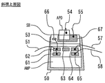
図2は、本発明の実施の形態にかかる半導体受光装置10の内部構成を示す図である。図3は、図2のX−X´線に沿う切断構造を矢印方向に見た図である。図4は、本発明の実施の形態にかかる半導体受光装置10のサブマウントSB等の周辺構成を拡大した斜視上面図である。図5は、本発明の実施の形態にかかる半導体受光装置10のサブマウントSBの上面の構成を示した図である。
FIG. 2 is a diagram showing an internal configuration of the semiconductor
なお、「サブマウントSBの上面」とは、サブマウントSBにおける窓14側を向く表面を意味するものとする。また、「サブマウント高周波アンプAMPの上面」とは、高周波アンプAMPにおける窓14側を向く表面を意味するものとする。
The “upper surface of the submount SB” means the surface of the submount SB facing the
図2乃至4に示すように、半導体受光装置10は、各種部品が実装されたヘッダ20を備えている。ヘッダ20は鍔部20a、円盤部20bおよび上面20cを有しており、この上面20cには高周波グランドパッド62を備えた高周波アンプAMPが設けられている。高周波アンプAMPは、半導体受光素子APDからの出力信号を増幅するアンプである。また、上面20cには、サブマウントSBが、高周波アンプAMPの隣に配置されている。
As shown in FIGS. 2 to 4, the semiconductor
サブマウントSBは、半導体受光素子APDがボンディングされる電極パッド67と、電極パッド67の隣に設けられた電極パッド66を有している。サブマウントSBの上面には、サブマウントSBの上面よりも小さな半導体受光素子APDがボンディングされている。半導体受光素子APDは、アバランシェフォトダイオードである。
The submount SB has an
ヘッダ20は表面に金メッキが施されている。高周波アンプAMPおよびサブマウントSBは、銀ペースト50によりヘッダ20上にボンディングされている。銀ペースト50は、銀およびバインダー樹脂を含む銀ペーストである。取付を銀ペーストで行うことで、生産性向上が可能なのである。ヘッダ20の上面20cには、キャパシタC1およびキャパシタC2も取り付けられている。
The
ヘッダ20は、リードピン22a、22b、22c、22d、22fを備えている。リードピン22は棒状端子であり、一例としてリードピン22が4本の場合であるが、さらに多くの本数のリードピン22が配設されている場合もある。半導体受光装置10は差動方式であり、2つの端子(リードピン22a、22b)からの出力となる。リードピン22fは、ヘッダ20の裏面であってリードピン22a、22bの間に溶接されている。このリードピン22fは、GNDを取るためのピンであり、ヘッダ20裏面に溶接されている。リードピン22fは他のリードピンとは異なりヘッダ20上面には現れてこず、また他のリードピンのようにヘッダ20との間にガラスハーメチックが介在することもなく、ヘッダ20とリードピン22fは電気的に接続している。
The
ヘッダ20は金属製、例えば直径が3〜10mm程度の鉄製の円板でリードピン22が挿入される貫通孔がリードピン22の個数に対応して、4個穿孔されている。リードピン22a,22b、22c、22dはガラス製のハーメチック24a、24b、24c、24dによりヘッダ20に固着される。またこのハーメチックにより貫通孔とリードピン22との隙間が封止されている。
The
ヘッダ20上の各構成は、信号線としてのワイヤ51〜58により電気的に接続されている。これらのワイヤ51〜58は、金属線であり、本実施の形態では金線とする。ワイヤ51は、高周波アンプAMPとリードピン22b先端とを接続する。ワイヤ52は、キャパシタC1とリードピン22d先端とを接続する。ワイヤ53は、高周波アンプAMPとサブマウントSBとを接続している。ワイヤ54は、半導体受光素子APDからの出力を高周波アンプAMPに伝えるように、これらを接続している。ワイヤ55は、キャパシタC1とサブマウントSBとを接続している。ワイヤ56は、キャパシタC2とリードピン22c先端とを接続している。ワイヤ57は、高周波アンプAMPとキャパシタC2とを接続している。ワイヤ58は、高周波アンプAMPとリードピン22a先端とを接続している。なお、図2および図4において、各ワイヤの端部のうち、黒丸の点を示した側の端部がボールボンディングにおけるファーストボンド接続が行われている部位であり、そうでない側の端部がセカンドボンドが行われている部位である。
Each component on the
図4に示すように、高周波アンプAMPは、その上面に電極パッド61、高周波グランドパッド62、電極パッド63、電極パッド64、および電極パッド65を備えている。各電極パッドに、上述したワイヤ51、53、54、57、58がボンディングされている。
As shown in FIG. 4, the high-frequency amplifier AMP includes an electrode pad 61, a high-
図5に示すように、サブマウントSBの上面には、電極パッド66および電極パッド67が設けられている。サブマウントSBは、長さLAの長辺と、長さLBの短辺とを備えている。本実施の形態では、電極パッド66は電極パッド67に比して十分に小さく、半導体受光素子APDはサブマウントSBのほぼ中央に位置するように電極パッド67にボンディングされている。
As shown in FIG. 5, an
高周波グランドパッド62と電極パッド66とが、ワイヤ53で接続されている。ワイヤ53のファーストボンドは高周波グランドパッド62であり、ワイヤ53のセカンドボンド位置が、電極パッド66である。サブマウントSBは一般にセラミック等の誘電体材料を用いているため、キャパシタとして働き、DCでは絶縁体であるがACの高周波領域では導電体として働く。よって、サブマウントSBを介して、ワイヤ53のグランド接続が可能となる。
The high
こうすることで、半導体受光素子APDよりもサブマウントSBの上面が大きい点を利用して、サブマウントSBの上面における空きスペースに高周波グランドパッド62を設けることができる。これにより、サブマウントSB上面のスペースを有効活用して高周波グランド用のワイヤ接続を確保できるので、ヘッダ20の上面20cへのワイヤボンディング数を減らすことができる。特に、本実施の形態では、ヘッダ20の上面20cへのワイヤボンディング数がゼロである。
By doing so, the high
また1つの部材(サブマウントSB)に複数の機能を持たせることで、省スペース化が可能となる。高周波グランド用のワイヤをヘッダに接合していた場合に必要であったヘッダ領域に空きが出来るなど、設計の自由度が増える。
また、本実施の形態では高周波アンプAMPとサブマウントSBの上面高さがほぼ同じである。このため、サブマウントSB上に2ndボンドを形成することで、高周波GND用のワイヤ53を非常に短くできる。その結果、ワイヤ53のインピーダンス(特にインダクタンス)を低減でき高速応答が可能となる。
Further, by providing a single member (submount SB) with a plurality of functions, space can be saved. The degree of freedom in design increases, for example, a space is created in the header area that was required when the high-frequency ground wire was joined to the header.
In the present embodiment, the top surface heights of the high-frequency amplifier AMP and the submount SB are substantially the same. For this reason, by forming a 2nd bond on the submount SB, the high-
なお、後述する図6との関係において、ヘッダ20の上面20cの法線方向に垂直な方向を高さ方向とする。この場合に、ヘッダ20上と高周波グランドパッド62との間の高さの差を第1の差Hとする。高周波グランドパッド62と電極パッド66との間の高さを第2の差hとする。本実施の形態では、サブマウントSBと高周波アンプAMPの高さが実質的に同じであり、第2の差hは実質的にゼロであるものとする。その結果、ほぼ同一の高さの2つの面の間でワイヤボンディングを実施することが可能となることで、ワイヤボンド作業の難易度が下がるという利点がある。
In the relationship with FIG. 6 described later, the direction perpendicular to the normal direction of the
ヘッダ20に対し、銀ペースト50でサブマウントSBや高周波アンプAMPを接合している。ここで、銀ペーストの種類によっては、ヘッダ20の表面の金メッキを伝わって樹脂成分が染み出し、ワイヤボンドの接合性に影響を及ぼすおそれがある。この点、本実施の形態によれば、サブマウントSB上に高周波グランド用のワイヤ53を接続してグランド接続を行うので、高周波アンプAMPとサブマウントSBの上面や側面には金メッキがない。よって、銀ペーストを使用してもワイヤボンド性の劣化を懸念しなくともよいという利点がある。
A submount SB and a high-frequency amplifier AMP are joined to the
[実施の形態の変形例]
図6は、本発明の実施の形態にかかる半導体受光装置10の変形例の構成を示す図である。サブマウントSBと高周波アンプAMPの高さが異なる場合であっても、第2の差hは第1の差Hよりも小さいことが好ましい。H>hであるため、上面20cにボンディングするよりも小さな高低差である第2の差hでワイヤボンディングできるようになり、ワイヤボンディング時におけるボンディング位置の高低差を抑制できる。結果、ワイヤボンド作業の難易度が下がるという利点がある。
[Modification of Embodiment]
FIG. 6 is a diagram showing a configuration of a modified example of the semiconductor
図7および図8は、本発明の実施の形態にかかる半導体受光装置10の変形例の構成を示す図である。図7に示すように、高周波アンプAMPとサブマウントSBが接するように、高周波アンプAMPとサブマウントSBは上面20cに隣接して配置されていてもよい。これにより、ワイヤ53、54の長さを極力短くすることができる。図7では簡単のため高周波アンプAMPの側面とサブマウントSBの側面がともに平坦であり、両側面を密着させた状態で図示している。しかし、実際の部品の構造によって、例えば高周波アンプAMPの側面に端子等の突起があった場合には、この突起をサブマウントSB側面に接触させることで「高周波アンプAMPとサブマウントSBが接する」ことになる。図8は、図7に示した構成の斜視上面図である。
7 and 8 are diagrams showing a configuration of a modified example of the semiconductor light-receiving
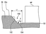
図9は、本発明の実施の形態の変形例にかかる半導体受光装置90を示す図である。半導体受光装置90は、ヘッダ20の上面20cに、凹部100を備えている。この凹部100内に高周波アンプAMPおよびサブマウントSBが設けられる点を除き、半導体受光装置10と同様の構成を備えている。凹部100は、底面104および底面を囲む側面102を備えている。底面104上に、高周波アンプAMPおよびサブマウントSBが銀ペースト50でボンディングされている。図10は凹部100内の構成を図示した斜視上面図であり、図11は図9のX2−X2´線に沿う断面構造を矢印方向に見た図である。凹部100により、高周波アンプAMPやサブマウントSB、半導体受光素子APDの高さが抑制されていることがわかる。また、キャパシタC1とサブマウントSBとを接続するワイヤ55の長さが抑制されたり、高さ位置をほぼ同一にでき、ワイヤボンディングの難易度低減も可能であることもわかる。図12は、図9のB−B´線に沿った断面構造のうち、高周波アンプAMP近傍を拡大した図である。図12に示すように、底面104と側面102とが90度を超える角度θで連結している。
FIG. 9 is a diagram showing a semiconductor
凹部100は通常、ヘッダ20の上面20cにプレス加工によって形成されるが、その場合、凹部100の縁辺部はR形状となる。このR形状により高周波アンプAMPを凹部100の縁に近づけるには限度がある。もし高周波グランドパッド62から上面20cにワイヤボンディングを行うと仮定すると、このワイヤ配線を短くするためにヘッダ20の上面のワイヤ領域へ近接して配置しようとしても、R形状に干渉しない範囲までしか近づけることができない。
The
また、プレス加工ではなく切削加工であれば、この縁辺部のR形状は解消できる。図13は、切削加工で凹部100を設けた場合におけるヘッダ20のB−B´線に沿った断面構造の高周波アンプAMP近傍を拡大した図である。しかし切削加工の場合、ヘッダの加工費が高くなる問題がある。また、切削加工であるとしても、図13のように距離L2は不可避的に発生してしまう。
Further, if the cutting process is performed instead of the pressing process, the R shape of the edge portion can be eliminated. FIG. 13 is an enlarged view of the vicinity of the high-frequency amplifier AMP having a cross-sectional structure taken along the line BB ′ of the
この点、本変形例にかかる半導体受光装置90では、高周波アンプAMPの高周波グランドパッド62からのワイヤ53は、上面20cではなく、サブマウントSBの電極パッド66に接続されている。したがって、凹部100との関係でワイヤ53を長くせざるを得ないという弊害を避けることができる。
In this regard, in the semiconductor
ここで、平面視において、「凹部100の縁」と「高周波グランドパッド62上のワイヤの接続点」との間の距離を第1距離とし、「高周波グランドパッド62上のワイヤの接続点」と「電極パッド66上のワイヤの接続点」との間の距離を第2距離とする。この場合において、第2の距離が第1の距離よりも小さい場合には、平面方向においてワイヤ長を短くすることができ、ワイヤ53が十分に短くされる。
Here, in plan view, the distance between “the edge of the
図14乃至20は、本発明の実施の形態にかかる半導体受光装置10が備えるサブマウントSBの変形例を示す図である。なお、図5との対比から明らかなとおり、図14乃至20における紙面下方側に高周波アンプAMPが存在している。これらの図は、それぞれ、サブマウントSB上に設けた電極パッドの構成を、上記実施の形態とは変更したものである。
図14のように、電極パッド66をより大面積な電極パッド200に変更しても良い。これに応じて、電極パッド67を電極パッド202に変更し、半導体受光素子APDを電極パッド202の高周波アンプAMP寄りの端にボンディングしてもよい。
図15のように、2つの電極パッド204、206を、ともに長さLA方向に伸びる長方形に形成したものとしても良い。そして、2つの電極パッド204、206を長さLB方向に平行に並べても良い。図15では高周波アンプAMP側に電極パッド206を設けている。
14 to 20 are views showing modifications of the submount SB included in the semiconductor
As shown in FIG. 14, the
As shown in FIG. 15, the two
サブマウントSB上の電極パターンを、インピーダンスが変わる程度に長方形もしくはさらに複雑なパターンにしてもよい。形状を変えることでインピーダンスを調整することができるからである。その結果、ワイヤ53やワイヤ55等のワイヤが接続される各電極パッドのインピーダンスを所望量に調節することができる。
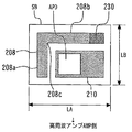
例えば、図16のように、平面視で、折れ曲がり部208cを備える電極パッド208を設けても良い。電極パッド208は、長さLB方向に伸びる第1部分208aと、長さLA方向に伸びる第2部分208bとを備え、これらの部分が折れ曲がり部208cにおいて角度90度で連結されている。また、電極パッド67に代えて電極パッド210が一回り小さく形成されている。
また、図17に示すように、平面視で、凹型の電極パッド212を設けても良い。電極パッド212は、サブマウントSBの図面左側端に配置された長さLB方向に伸びる第1部分212aと、サブマウントSBの高周波アンプAMP側と反対側の端に配置された長さLA方向に伸びる第2部分212bと、サブマウントSBの図面右側端に配置された長さLB方向に伸びる第3部分212eと、を備えている。第3部分212eは、第1部分212aと比べて、LB方向の長さが短く、かつLA方向の幅が太い。これらの3つの部分が折れ曲がり部212cおよび212dを介してそれぞれ角度90度で連結されている。この凹部の凹んだ位置に入り込むように電極パッド214が形成されており、電極パッド214はちょうど電極パッド212で囲まれるようにサブマウントSBの中央付近に配置された主部214aを備えている。この主部214aに半導体受光素子APDがボンディングされている。また、電極パッド214は第3部分212e側に突き出た凸部214bを備えている。
The electrode pattern on the submount SB may be a rectangle or a more complicated pattern that changes the impedance. This is because the impedance can be adjusted by changing the shape. As a result, the impedance of each electrode pad to which wires such as the
For example, as shown in FIG. 16, an
In addition, as shown in FIG. 17, a
図18のように、図16の電極パッド208を180度回転させた電極パッド216を設けても良い。これに応じて、電極パッド218およびこれにボンディングされる半導体受光素子APDの位置も調節すればよい。
なお、上記変形例では、ワイヤ53を介して高周波グランドパッド62と電気的に接続される電極パッド66を、折れ曲がり部を備えるL字型や凹型の電極パッドに変更した。しかしながら、折れ曲がり部以外にも、電極パッドの一部を部分的に突き出た形状とした凸部を設けてもよい。この折れ曲がり部と凸部の両方を設けても良い。
As shown in FIG. 18, an
In the modification, the
図19に示すように、電極パッド208の第2部分208b側の先端に、抵抗パターン部230を設けても良い。つまり、電極パッド208を、電極パッド210と同材料の導電体パターン部と、この導電体パターン部より高抵抗の抵抗パターン部230とを有するようにしてもよい。また、図20のように、抵抗パターン部230を、第2部分208bの途中(中央部付近)に設けても良い。このようにして、インピーダンスを調節することができる。
As shown in FIG. 19, a
図21は、本発明の実施の形態の変形例にかかる半導体受光装置を示す図であり、図3等に示した位置、断面に相当するものである。図21の変形例では、ワイヤ53を、あえて高さHwだけワイヤ立ち上げ部を長く形成したワイヤ253としている。例えば200μm以上とすることができる。こうすることで、ワイヤ長の調整が可能となり、インピーダンスの調節が可能となる。
FIG. 21 is a view showing a semiconductor light receiving device according to a modification of the embodiment of the present invention, and corresponds to the position and cross section shown in FIG. In the modification of FIG. 21, the
[実施の形態に対する比較例]
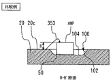
図22乃至24は、本発明の実施の形態にかかる半導体受光装置に対する比較例を示す図である。この比較例は、ワイヤ53に代えてワイヤ353が設けられている点およびサブマウントSBに電極パッド66が設けられていない点を除き、実施の形態の変形例にかかる半導体受光装置90と同様の構成を備えている。ワイヤ353は、高周波アンプAMPの高周波グランドパッド62にその一端がファーストボンドされ、その他端がヘッダ20の上面20cにセカンドボンドされている。
[Comparative example to the embodiment]
22 to 24 are diagrams showing comparative examples for the semiconductor light receiving device according to the embodiment of the present invention. This comparative example is the same as the semiconductor
図23は図22のA−A´断面構造を矢視方向に見た図であり、図24は図22のB−B´断面構造を示す図である。ワイヤ353は、高低差の大きい2つの面である高周波グランドパッド62と上面20cとの間でワイヤボンディングされなければならない。これはワイヤボンディングの難易度が増加し、製造上好ましくない。また、ワイヤ長の観点からしても、ボンディングする2つの面の高低差の分だけ不可避的にワイヤを長く取らざるを得ないという欠点がある。この点、本実施の形態にかかる半導体受光装置10、90では、ワイヤ53が高周波グランドパッド62と電極パッド66との間でワイヤボンディングされ、かつ、高周波グランドパッド62と電極パッド66の高低差が小さいので(ほぼ同一高さであるので)、ボンディング難易度を低減し、ワイヤ長を短く抑えることができる。一例としては100μm程度の短縮化が可能である。
23 is a view of the AA ′ cross-sectional structure of FIG. 22 as viewed in the direction of the arrow, and FIG. 24 is a view showing the BB ′ cross-sectional structure of FIG. The
また、図24に示すように、平面方向においても、側面102の分だけ、上面20cにおけるワイヤ353のセカンドボンド位置を、ずらさざるを得ない。これは、図12および図13を用いて説明した理由からである。つまり、高周波アンプAMPを凹部100の縁に近づけるには限度があるのである。この点、本変形例にかかる半導体受光装置90では、高周波アンプAMPの高周波グランドパッド62からのワイヤ53は、上面20cではなく、サブマウントSBの電極パッド66に接続されている。したがって、凹部100との関係でワイヤ53を長くせざるを得ないという弊害を避けることができる。
Also, as shown in FIG. 24, the second bond position of the
10、90 半導体受光装置、12 キャップ、14 窓、20 ヘッダ、20a 鍔部、20b 円盤部、20c 上面、22、22a、22b、22c、22d、22f リードピン、24a、24b、24c、24d ハーメチック、50 銀ペースト、51、52、53、54、55、56、57、58、253、353 ワイヤ、61、63、64、65、66、67 電極パッド、62 高周波グランドパッド、100 凹部、102 側面、104 底面、200、202、204、206、208、210、212、214、216、218 電極パッド、230 抵抗パターン部、AMP 高周波アンプ、APD 半導体受光素子、C1、C2 キャパシタ、SB サブマウント 10, 90 Semiconductor light receiving device, 12 cap, 14 window, 20 header, 20a collar, 20b disk portion, 20c top surface, 22, 22a, 22b, 22c, 22d, 22f lead pin, 24a, 24b, 24c, 24d hermetic, 50 Silver paste, 51, 52, 53, 54, 55, 56, 57, 58, 253, 353 Wire, 61, 63, 64, 65, 66, 67 Electrode pad, 62 High frequency ground pad, 100 Recess, 102 Side, 104 Bottom, 200, 202, 204, 206, 208, 210, 212, 214, 216, 218 Electrode pad, 230 Resistance pattern part, AMP high frequency amplifier, APD semiconductor light receiving element, C1, C2 capacitor, SB submount
Claims (7)
前記ヘッダ上に設けられ、上面を有しこの上面に高周波グランドパッドが備えられた高周波アンプと、
前記ヘッダ上に設けられ、誘電体材料で形成され、上面を有するサブマウントと、
前記サブマウントの上面に設けられ、前記サブマウントの上面よりも小さな平面寸法を有する半導体受光素子と、
を備え、
前記サブマウントの上面は、前記半導体受光素子がボンディングされた第1電極パッドと、前記第1電極パッドの隣に前記第1電極パッドから離れて設けられた第2電極パッドを有し、
前記第2電極パッド、前記ヘッダ、および前記第2電極パッドと前記ヘッダとで挟まれた前記サブマウントにより、キャパシタが構成され、
前記高周波グランドパッドと前記第2電極パッドとがワイヤで接続されたことを特徴とする半導体受光装置。 A header formed of a conductive material ;
A high frequency amplifier provided on the header and having a top surface and a high frequency ground pad on the top surface;
A submount provided on the header, formed of a dielectric material and having an upper surface;
A semiconductor light receiving element provided on the upper surface of the submount and having a smaller planar dimension than the upper surface of the submount;
With
The upper surface of the submount includes a first electrode pad to which the semiconductor light receiving element is bonded, and a second electrode pad provided next to the first electrode pad and separated from the first electrode pad,
A capacitor is configured by the second electrode pad, the header, and the submount sandwiched between the second electrode pad and the header,
A semiconductor light receiving device, wherein the high-frequency ground pad and the second electrode pad are connected by a wire.
前記凹部は、底面および前記底面を囲む側面を備え、前記底面と前記側面とが成す角度が90度を超えるように前記底面と前記側面とが連結しており、
前記底面上に、前記高周波アンプおよび前記サブマウントが設けられており、
前記ヘッダの上面の平面視において、前記凹部の外周の縁と前記高周波グランドパッド上において前記ワイヤが接続された接続点との間の距離を第1距離とし、前記接続点と前記第2電極パッド上において前記ワイヤが接続された接続点との間の距離を第2距離とし、前記第2距離は前記第1距離よりも小さいことを特徴とする請求項1乃至3のいずれか1項に記載の半導体受光装置。 The header includes a recess;
The recess includes a bottom surface and a side surface surrounding the bottom surface, and the bottom surface and the side surface are connected so that an angle formed by the bottom surface and the side surface exceeds 90 degrees,
The high-frequency amplifier and the submount are provided on the bottom surface,
In plan view of the upper surface of the header, a distance between an outer peripheral edge of the recess and a connection point to which the wire is connected on the high-frequency ground pad is defined as a first distance, and the connection point and the second electrode pad The distance between the connection point to which the wire is connected above is a second distance, and the second distance is smaller than the first distance. Semiconductor light receiving device.
前記高周波アンプおよび前記サブマウントの少なくとも一方は、銀およびバインダー樹脂を含む銀ペーストにより、前記ヘッダ上にボンディングされていることを特徴とする請求項1乃至4のいずれか1項に記載の半導体受光装置。 The header is gold plated on the surface,
5. The semiconductor light receiving device according to claim 1, wherein at least one of the high-frequency amplifier and the submount is bonded onto the header with a silver paste containing silver and a binder resin. 6. apparatus.
Priority Applications (3)
| Application Number | Priority Date | Filing Date | Title |
|---|---|---|---|
| JP2013025660A JP6127561B2 (en) | 2013-02-13 | 2013-02-13 | Semiconductor photo detector |
| US14/065,477 US9329077B2 (en) | 2013-02-13 | 2013-10-29 | Semiconductor photodetector device |
| CN201310614577.7A CN103985768B (en) | 2013-02-13 | 2013-11-28 | Quasiconductor optical pickup apparatus |
Applications Claiming Priority (1)
| Application Number | Priority Date | Filing Date | Title |
|---|---|---|---|
| JP2013025660A JP6127561B2 (en) | 2013-02-13 | 2013-02-13 | Semiconductor photo detector |
Publications (3)
| Publication Number | Publication Date |
|---|---|
| JP2014154823A JP2014154823A (en) | 2014-08-25 |
| JP2014154823A5 JP2014154823A5 (en) | 2016-01-21 |
| JP6127561B2 true JP6127561B2 (en) | 2017-05-17 |
Family
ID=51277667
Family Applications (1)
| Application Number | Title | Priority Date | Filing Date |
|---|---|---|---|
| JP2013025660A Active JP6127561B2 (en) | 2013-02-13 | 2013-02-13 | Semiconductor photo detector |
Country Status (3)
| Country | Link |
|---|---|
| US (1) | US9329077B2 (en) |
| JP (1) | JP6127561B2 (en) |
| CN (1) | CN103985768B (en) |
Families Citing this family (4)
| Publication number | Priority date | Publication date | Assignee | Title |
|---|---|---|---|---|
| JP2017126949A (en) * | 2016-01-15 | 2017-07-20 | 国立研究開発法人情報通信研究機構 | Photoelectric converter |
| CN106024649A (en) * | 2016-07-12 | 2016-10-12 | 希睿(厦门)科技有限公司 | Ultra-thin ambient light and proximity sensor wafer level package and package method thereof |
| JP1624076S (en) * | 2018-04-16 | 2019-02-12 | ||
| CN111146296A (en) * | 2018-11-05 | 2020-05-12 | 上海集耀电子有限公司 | Improved photosensitive receiving tube |
Family Cites Families (10)
| Publication number | Priority date | Publication date | Assignee | Title |
|---|---|---|---|---|
| JPH054534U (en) | 1991-02-18 | 1993-01-22 | 三菱電機株式会社 | Laser diode chip carrier |
| JP2002289956A (en) * | 2001-03-22 | 2002-10-04 | Kyocera Corp | Semiconductor laser device |
| JP2003134051A (en) * | 2001-10-25 | 2003-05-09 | Opnext Japan Inc | Optical receiving module, optical receiver and optical fiber communication equipment |
| KR100575950B1 (en) * | 2003-06-20 | 2006-05-02 | 삼성전자주식회사 | Optical receiver module with to can structure |
| JP2006114635A (en) * | 2004-10-13 | 2006-04-27 | Sharp Corp | Semiconductor device |
| JP2006253676A (en) * | 2005-03-08 | 2006-09-21 | Sumitomo Electric Ind Ltd | Optical assembly |
| US8059973B2 (en) * | 2006-02-17 | 2011-11-15 | Finisar Corporation | Discrete bootstrapping in an optical receiver to prevent signal feedback |
| JP4970924B2 (en) * | 2006-03-28 | 2012-07-11 | 三菱電機株式会社 | Optical element package and optical semiconductor device using the same |
| CN100592585C (en) * | 2006-03-28 | 2010-02-24 | 三菱电机株式会社 | Optical device package and optical semiconductor device using the same |
| JP2010251570A (en) * | 2009-04-16 | 2010-11-04 | Mitsubishi Electric Corp | Optical receiving module |
-
2013
- 2013-02-13 JP JP2013025660A patent/JP6127561B2/en active Active
- 2013-10-29 US US14/065,477 patent/US9329077B2/en active Active
- 2013-11-28 CN CN201310614577.7A patent/CN103985768B/en active Active
Also Published As
| Publication number | Publication date |
|---|---|
| US9329077B2 (en) | 2016-05-03 |
| US20140224967A1 (en) | 2014-08-14 |
| CN103985768B (en) | 2016-10-26 |
| CN103985768A (en) | 2014-08-13 |
| JP2014154823A (en) | 2014-08-25 |
Similar Documents
| Publication | Publication Date | Title |
|---|---|---|
| KR100939402B1 (en) | Semiconductor device | |
| JP5001872B2 (en) | Semiconductor device | |
| US5814871A (en) | Optical semiconductor assembly having a conductive float pad | |
| WO2021020480A1 (en) | Electronic component mounting package, and electronic device | |
| US8836106B2 (en) | Semiconductor device | |
| JP2509422B2 (en) | Semiconductor device and manufacturing method thereof | |
| US20040089921A1 (en) | Lead frame and method of producing the same, and resin-encapsulated semiconductor device and method of producing the same | |
| JP6127561B2 (en) | Semiconductor photo detector | |
| CN104350586A (en) | Semiconductor device | |
| JPWO2018123064A1 (en) | Semiconductor device | |
| US9106047B2 (en) | Optical semiconductor element package and optical semiconductor device | |
| JP2003258272A (en) | Optical signal receiving module | |
| CN110663109A (en) | Semiconductor device with a plurality of semiconductor chips | |
| KR20080022509A (en) | Microphone package | |
| JP2004179303A (en) | Element package and its manufacturing method | |
| JP2004095869A (en) | Light receiving element and light receiving device | |
| JP4045830B2 (en) | Receiver module | |
| JP2010251570A (en) | Optical receiving module | |
| US6949731B2 (en) | Light-receiving module having a light-receiving device on a die-capacitor | |
| JP2007141947A (en) | Semiconductor device and its manufacturing method | |
| JP2005150294A (en) | Semiconductor device and its manufacturing method | |
| JP2000307020A (en) | Package for high frequency device | |
| JP7158199B2 (en) | semiconductor equipment | |
| EP4174927A1 (en) | Wiring substrate and electronic device | |
| JP2003007954A (en) | Manufacturing method for resin-sealing semiconductor device |
Legal Events
| Date | Code | Title | Description |
|---|---|---|---|
| A521 | Request for written amendment filed |
Free format text: JAPANESE INTERMEDIATE CODE: A523 Effective date: 20151125 |
|
| A621 | Written request for application examination |
Free format text: JAPANESE INTERMEDIATE CODE: A621 Effective date: 20151125 |
|
| A977 | Report on retrieval |
Free format text: JAPANESE INTERMEDIATE CODE: A971007 Effective date: 20160720 |
|
| A131 | Notification of reasons for refusal |
Free format text: JAPANESE INTERMEDIATE CODE: A131 Effective date: 20160726 |
|
| A521 | Request for written amendment filed |
Free format text: JAPANESE INTERMEDIATE CODE: A523 Effective date: 20160906 |
|
| A02 | Decision of refusal |
Free format text: JAPANESE INTERMEDIATE CODE: A02 Effective date: 20161206 |
|
| A521 | Request for written amendment filed |
Free format text: JAPANESE INTERMEDIATE CODE: A523 Effective date: 20170209 |
|
| A911 | Transfer to examiner for re-examination before appeal (zenchi) |
Free format text: JAPANESE INTERMEDIATE CODE: A911 Effective date: 20170221 |
|
| TRDD | Decision of grant or rejection written | ||
| A01 | Written decision to grant a patent or to grant a registration (utility model) |
Free format text: JAPANESE INTERMEDIATE CODE: A01 Effective date: 20170314 |
|
| A61 | First payment of annual fees (during grant procedure) |
Free format text: JAPANESE INTERMEDIATE CODE: A61 Effective date: 20170327 |
|
| R150 | Certificate of patent or registration of utility model |
Ref document number: 6127561 Country of ref document: JP Free format text: JAPANESE INTERMEDIATE CODE: R150 |
|
| R250 | Receipt of annual fees |
Free format text: JAPANESE INTERMEDIATE CODE: R250 |
|
| R250 | Receipt of annual fees |
Free format text: JAPANESE INTERMEDIATE CODE: R250 |
|
| R250 | Receipt of annual fees |
Free format text: JAPANESE INTERMEDIATE CODE: R250 |
|
| R250 | Receipt of annual fees |
Free format text: JAPANESE INTERMEDIATE CODE: R250 |
|
| R250 | Receipt of annual fees |
Free format text: JAPANESE INTERMEDIATE CODE: R250 |