JP6120761B2 - Optical transmitter and method for controlling optical transmitter - Google Patents
Optical transmitter and method for controlling optical transmitter Download PDFInfo
- Publication number
- JP6120761B2 JP6120761B2 JP2013256685A JP2013256685A JP6120761B2 JP 6120761 B2 JP6120761 B2 JP 6120761B2 JP 2013256685 A JP2013256685 A JP 2013256685A JP 2013256685 A JP2013256685 A JP 2013256685A JP 6120761 B2 JP6120761 B2 JP 6120761B2
- Authority
- JP
- Japan
- Prior art keywords
- optical
- bias voltage
- light
- unit
- modulators
- Prior art date
- Legal status (The legal status is an assumption and is not a legal conclusion. Google has not performed a legal analysis and makes no representation as to the accuracy of the status listed.)
- Active
Links
- 230000003287 optical effect Effects 0.000 title claims description 445
- 238000000034 method Methods 0.000 title claims description 37
- 238000001514 detection method Methods 0.000 claims description 43
- 230000007274 generation of a signal involved in cell-cell signaling Effects 0.000 claims description 17
- 230000001419 dependent effect Effects 0.000 claims 1
- 230000010363 phase shift Effects 0.000 description 33
- 230000001360 synchronised effect Effects 0.000 description 22
- 230000008033 biological extinction Effects 0.000 description 10
- 238000010586 diagram Methods 0.000 description 8
- 238000006243 chemical reaction Methods 0.000 description 6
- 238000004891 communication Methods 0.000 description 5
- 230000000694 effects Effects 0.000 description 5
- 239000013598 vector Substances 0.000 description 5
- 238000012544 monitoring process Methods 0.000 description 4
- 238000012545 processing Methods 0.000 description 4
- 239000013307 optical fiber Substances 0.000 description 3
- 230000032683 aging Effects 0.000 description 2
- 239000000470 constituent Substances 0.000 description 2
- 239000013078 crystal Substances 0.000 description 2
- GQYHUHYESMUTHG-UHFFFAOYSA-N lithium niobate Chemical compound [Li+].[O-][Nb](=O)=O GQYHUHYESMUTHG-UHFFFAOYSA-N 0.000 description 2
- 239000000463 material Substances 0.000 description 2
- 239000004065 semiconductor Substances 0.000 description 2
- 239000000758 substrate Substances 0.000 description 2
- -1 InP compound Chemical class 0.000 description 1
- 230000005540 biological transmission Effects 0.000 description 1
- 238000004364 calculation method Methods 0.000 description 1
- 238000004590 computer program Methods 0.000 description 1
- 230000005684 electric field Effects 0.000 description 1
- 239000000284 extract Substances 0.000 description 1
- 238000012538 light obscuration Methods 0.000 description 1
- 238000000926 separation method Methods 0.000 description 1
Images


Classifications
-
- H—ELECTRICITY
- H04—ELECTRIC COMMUNICATION TECHNIQUE
- H04B—TRANSMISSION
- H04B10/00—Transmission systems employing electromagnetic waves other than radio-waves, e.g. infrared, visible or ultraviolet light, or employing corpuscular radiation, e.g. quantum communication
- H04B10/50—Transmitters
- H04B10/501—Structural aspects
- H04B10/503—Laser transmitters
- H04B10/505—Laser transmitters using external modulation
- H04B10/5057—Laser transmitters using external modulation using a feedback signal generated by analysing the optical output
- H04B10/50575—Laser transmitters using external modulation using a feedback signal generated by analysing the optical output to control the modulator DC bias
-
- H—ELECTRICITY
- H04—ELECTRIC COMMUNICATION TECHNIQUE
- H04B—TRANSMISSION
- H04B10/00—Transmission systems employing electromagnetic waves other than radio-waves, e.g. infrared, visible or ultraviolet light, or employing corpuscular radiation, e.g. quantum communication
- H04B10/50—Transmitters
- H04B10/501—Structural aspects
- H04B10/503—Laser transmitters
- H04B10/505—Laser transmitters using external modulation
- H04B10/5053—Laser transmitters using external modulation using a parallel, i.e. shunt, combination of modulators
Description
本発明は光送信器および光送信器の制御方法に関し、特に、入射光を変調する光変調部と、光変調部に変調信号を入力する変調信号駆動部と、光変調部および前記変調信号駆動部を制御する制御部とを備える光送信器に関する。 The present invention relates to an optical transmitter and a method for controlling the optical transmitter, and in particular, an optical modulation unit that modulates incident light, a modulation signal drive unit that inputs a modulation signal to the optical modulation unit, an optical modulation unit, and the modulation signal drive The present invention relates to an optical transmitter including a control unit that controls the unit.
MZ(Mach−Zehnder)型光変調器の最適なバイアス電圧は、温度や経年変動によってドリフトしていくことが知られている。そのため、送信光信号の品質を保つために、バイアス電圧を最適なバイアス値に追従させる制御が行われている。例えば、I/Q変調器の自動バイアス制御(ABC:automatic bias control)を行う光送信器において、任意電気波形が入力された状態で、I−ch、Q−ch、Phaseの3つのバイアス電圧を順番に制御し、このとき、I−ch、Q−chのバイアス電圧に低周波信号(Dither)を重畳し、モニタPD(Photo−Diode)電流から検出されるDitherの誤差信号が0となる収束点にフィードバック制御を行うものが知られている。 It is known that the optimum bias voltage of an MZ (Mach-Zehnder) type optical modulator drifts with temperature and aging. For this reason, in order to maintain the quality of the transmission optical signal, control is performed so that the bias voltage follows the optimum bias value. For example, in an optical transmitter that performs automatic bias control (ABC) of an I / Q modulator, three bias voltages of I-ch, Q-ch, and Phase are set while an arbitrary electric waveform is input. In this case, the low-frequency signal (Dither) is superimposed on the I-ch and Q-ch bias voltages, and the Dither error signal detected from the monitor PD (Photo-Diode) current becomes zero. One that performs feedback control on a point is known.
特許文献1に開示されている光送信器においては、光変調部のCW(Continuous Wave)光出力が最も消光する時の第1、第2のマッハツェンダ変調器のそれぞれに印加するバイアス電圧の初期値の探索方法として、第1、第2のマッハツェンダ変調器のそれぞれのバイアス電圧と、光位相調整部のバイアス電圧の計3点を各々±Vπの範囲で変動させて、光出力レベルをモニタして決定する。第1、第2のマッハツェンダ変調器の合成光しかモニタすることができないため、合成光が消光状態であっても、第1、第2のマッハツェンダ変調器からの出力光が互いに逆位相である可能性がある。そのため、第1、第2のマッハツェンダ変調器からの出力光がそれぞれ消光状態であるかを判定するのが困難であった。そのため、特許文献1の方式においては、第1、第2のマッハツェンダ変調器のそれぞれのバイアス電圧と、光位相調整部のバイアス電圧の計3点を組合せて最適なバイアス電圧を決定する。よって、長い時間が掛かってしまうという問題があった。 In the optical transmitter disclosed in Patent Document 1, the initial value of the bias voltage applied to each of the first and second Mach-Zehnder modulators when the CW (Continuous Wave) optical output of the optical modulator is most extinguished. As a search method, a total of three bias voltages of the first and second Mach-Zehnder modulators and a bias voltage of the optical phase adjusting unit are varied within a range of ± Vπ, and the optical output level is monitored. decide. Since only the combined light of the first and second Mach-Zehnder modulators can be monitored, the output light from the first and second Mach-Zehnder modulators can be in opposite phases even when the combined light is in the extinction state There is sex. Therefore, it is difficult to determine whether the output light from the first and second Mach-Zehnder modulators is in the extinction state. Therefore, in the method of Patent Document 1, an optimum bias voltage is determined by combining a total of three points of the bias voltages of the first and second Mach-Zehnder modulators and the bias voltage of the optical phase adjustment unit. Therefore, there is a problem that it takes a long time.
本発明は、以上のような課題を解決するためになされたものであり、2つの変調器のそれぞれに印加するバイアス電圧の初期値を短時間で決定することが可能な、光送信器および光送信器の制御方法の提供を目的とする。 The present invention has been made to solve the above-described problems, and an optical transmitter and an optical device capable of quickly determining an initial value of a bias voltage applied to each of two modulators. An object is to provide a method for controlling a transmitter.
本発明に係る光送信器は、入射光を変調する光変調部と、光変調部に変調信号を入力する変調信号駆動部と、光変調部および変調信号駆動部を制御する制御部と、を備える光送信器であって、光変調部は、光源から入射した光を2つの光に分岐する分岐部と、印加されたバイアス電圧および入力された変調信号に基づいて前記2つの光のそれぞれを変調するマッハツェンダ型の2つの光変調器と、2つの光変調器のいずれかに接続され、印加されたバイアス電圧に基づいて当該光変調器に入射する光の位相を調整する光位相調整部と、2つの光変調器からの出力光を合波して出力する合波部と、合波部から出力される光の強度を検出する光強度検出部と、を備え、変調信号駆動部は、前記2つの光変調器の各々に前記変調信号を入力し、制御部は、変調信号が入力されない状態としての初期状態において2つの光変調器に印加されるバイアス電圧を探索して決定する制御部であって、制御部は、前記2つの光変調器の各々に変調信号が入力されない状態において、2つの光変調器のうち一方の光変調器および光位相調整部に印加するバイアス電圧を一定に保ちながら、光強度検出部が検出する光の強度に基づいて、2つの光変調器のうち他方の光変調器からの出力光がゼロになるように、当該他方の光変調器に印加するバイアス電圧を第1初期バイアス電圧として決定し、その後に、当該他方の光変調器に第1初期バイアス電圧を印加し、かつ、光位相調整部に印加するバイアス電圧を一定に保ちながら、光強度検出部が検出する光の強度に基づいて、一方の光変調器からの出力光がゼロになるように、当該一方の光変調器に印加するバイアス電圧を第2初期バイアス電圧として決定し、制御部は、他方の光変調器に印加するバイアス電圧を変化させることにより、光強度検出部が検出する光の強度が最大となるバイアス電圧と、当該バイアス電圧に隣接し、かつ光強度検出部が検出する光の強度が極大となるバイアス電圧とを探索し、2つのバイアス電圧を加算して2で割った値を、他方の光変調器からの出力光がゼロになる第1初期バイアス電圧として決定することを特徴とする。 An optical transmitter according to the present invention includes an optical modulation unit that modulates incident light, a modulation signal driving unit that inputs a modulation signal to the optical modulation unit, and a control unit that controls the optical modulation unit and the modulation signal driving unit. An optical transmitter comprising: a branching unit that splits light incident from a light source into two lights; and each of the two lights based on an applied bias voltage and an input modulation signal Two optical modulators of Mach-Zehnder type to be modulated, and an optical phase adjusting unit that is connected to one of the two optical modulators and adjusts the phase of light incident on the optical modulator based on an applied bias voltage; A multiplexing unit that combines and outputs the output light from the two optical modulators, and a light intensity detection unit that detects the intensity of the light output from the multiplexing unit, the modulation signal driving unit, The modulation signal is input to each of the two optical modulators and controlled. Is a control unit that searches and determines a bias voltage applied to the two optical modulators in an initial state where no modulation signal is input, and the control unit modulates each of the two optical modulators. Based on the intensity of light detected by the light intensity detector, while maintaining a constant bias voltage applied to one of the two optical modulators and the optical phase adjuster in a state where no signal is input, 2 The bias voltage applied to the other optical modulator is determined as the first initial bias voltage so that the output light from the other optical modulator of the two optical modulators becomes zero, and then the other light modulator While applying the first initial bias voltage to the modulator and keeping the bias voltage applied to the optical phase adjustment unit constant, based on the light intensity detected by the light intensity detection unit, Output light To be zero, to determine the bias voltage applied to one of the optical modulator the as the second initial bias voltage, the control unit, by changing the bias voltage applied to the other light modulator, the light intensity detection Search for the bias voltage that maximizes the light intensity detected by the unit and the bias voltage that is adjacent to the bias voltage and that maximizes the light intensity detected by the light intensity detection unit, and add the two bias voltages Then, the value divided by 2 is determined as the first initial bias voltage at which the output light from the other optical modulator becomes zero.
本発明に係る光送信器によれば、他方の光送信器の第1初期バイアス電圧を探索する際には、一方の光変調器および光位相調整部に印加するバイアス電圧を一定値に固定する。そして、第1の初期バイアス電圧を決定した後に、一方の光変調器の第2の初期バイアス電圧を探索する際には、他方の光変調器および光位相調整部に印加するバイアス電圧の値を一定値に固定する。よって、本発明に係る光送信器は、2つの光変調器のバイアス電圧を同時に変化させながら探索を行うのではなく、一方の光変調器のバイアス電圧を固定した状態で他方の光変調器のバイアス電圧の探索を行うため、より高速に第1、第2の初期バイアス電圧の探索を完了することが可能である。 According to the optical transmitter of the present invention, when searching for the first initial bias voltage of the other optical transmitter, the bias voltage applied to one of the optical modulator and the optical phase adjustment unit is fixed to a constant value. . Then, after searching for the first initial bias voltage, when searching for the second initial bias voltage of one of the optical modulators, the value of the bias voltage applied to the other optical modulator and the optical phase adjusting unit is set. Fix to a fixed value. Therefore, the optical transmitter according to the present invention does not perform a search while simultaneously changing the bias voltages of the two optical modulators, but with the bias voltage of one optical modulator fixed, Since the search for the bias voltage is performed, the search for the first and second initial bias voltages can be completed at a higher speed.
<実施の形態1>
<構成>
図1は、本実施の形態における光送信器の機能ブロック図である。本実施の形態における光送信器は、入力される変調信号および入力されるバイアス電圧に基づいて、光源1から入射する光線を変調する光変調部100と、変調信号を光変調部100に入力する変調信号駆動部2と、光変調部100および変調信号駆動部2の動作を制御する制御部200を備える。光源1と光変調部100は、例えば光ファイバにより光学的に接続されている。
<Embodiment 1>
<Configuration>
FIG. 1 is a functional block diagram of an optical transmitter according to the present embodiment. The optical transmitter according to the present embodiment inputs an
光変調部100は、第1の光変調器101、第2の光変調器102および光位相調整部103を備える。第1、第2の光変調器101,102および光位相調整部103は、例えばニオブ酸リチウムを含む基板に形成されている。また、基板上には光導波路105a〜105gが形成されている。
The
図1に示すように、光源1からの光が入射する光導波路105aは光導波路105bと光導波路105cに分岐して第1、第2の光変調器101,102のそれぞれの入力側に接続されている。第2の光変調器102の出力側は光導波路105eを介して光位相調整部103に接続されている。第1の光変調器101、光位相調整部103からの出射光は光導波路105d,105fを介して光導波路105gにおいて合波されて光変調部100から出力される。また、光導波路105gを通過する光の一部は、光強度検出部104に入射する。
As shown in FIG. 1, an
第1、第2の光変調器101,102はマッハツェンダ型光変調器である。第1、第2の光変調器101,102のそれぞれには変調信号駆動部2から変調信号が入力される。また、第1、第2の光変調器101,102および光位相調整部には制御部200からバイアス電圧が入力される。
The first and second
光強度検出部104に引き込まれた合成光の一部は、光強度に応じた電流信号に変換される。電流信号は、電流電圧変換部3で電圧信号に変換され、制御部200に備わるモニタ部204に入力される。
A part of the combined light drawn into the light
図1において、制御部200は、同期検波部201、バイアス印加部202a、202b、202c、モニタ部204を備える。同期検波部201は、モニタ部204に入力された電圧信号を元に、初期値探索状態として第1、第2の光変調器101,102に印加するバイアス電圧の初期値を求める。同期検波部201の動作については後述する。
In FIG. 1, the
バイアス印加部202a,202b,202cは、第1の光変調器101、第2の光変調器102、光位相調整部103のそれぞれにバイアス電圧を印加する。
The
光源1は、例えばInP系化合物半導体混晶を構成材料とする半導体レーザであり、1.5μm波長帯の連続波としてのレーザ光を発光して出力する。なお、光源1の構成は、これに限られるものではなく、例えば1.3μm波長帯や、パルス波や、固体レーザ等を用いるようにしても良く、要するに所望の光通信を実現するための光を発光するものを、この発明の実施の形態として適用可能である。 The light source 1 is a semiconductor laser having, for example, an InP compound semiconductor mixed crystal as a constituent material, and emits and outputs laser light as a continuous wave in a 1.5 μm wavelength band. The configuration of the light source 1 is not limited to this. For example, a 1.3 μm wavelength band, a pulse wave, a solid-state laser, or the like may be used. In short, light for realizing desired optical communication is used. Can be applied as an embodiment of the present invention.
また、第1、第2の光変調器101,102は、例えばニオブ酸リチウム結晶を構成材料とし、電界印加による屈折率変化、いわゆる電気光学効果を利用したマッハツェンダ型光変調器である。マッハツェンダ型光変調器は、2つのY分岐光導波路の間に、電極を形成した2本の光導波路を並列に接続して、いわゆるマッハツェンダ干渉計として構成されている。マッハツェンダ型光変調器は、マッハツェンダ干渉計を通過する光に対して、変調電極に入力された変調信号およびバイアス電極に印加されたバイアス電圧による屈折率変化に起因する2本の光導波路の間の位相差に応じた光強度変化を与えて出力する。マッハツェンダ型光変調器は、低チャープといった高い信号品質と高速性の両立が可能な光変調器である。
The first and second
また、光変調部100は、第1、第2の光変調器101,102としての2個のマッハツェンダ型光変調器をマッハツェンダ干渉計として並列に接続し、実数部であるIch(In−phase channel)光信号と虚数部であるQch(Quadrature−phase channel)光信号とを、π/2の搬送波位相差を与えて合波することで、複素光電界を生成する2並列MZ型光変調器(DP−MZM:dual−parallel Mach−Zehnder modulator)である。2並列MZ型光変調器はI/Q変調器とも呼ばれる。
The
光変調部100において、第1、第2の光変調器101,102は変調信号が入力される変調電極と、バイアス電圧が印加されるバイアス電極を備えている。また、各マッハツェンダ型光変調器を並列に接続する光導波路の片方に光位相調整部103としての位相制御電極PS(Phase Shift)を備えている。
In the
なお、光変調部100、第1の光変調器101、第2の光変調器102の構成は、これに限られるものではなく、最適なバイアス電圧が温度や経年変動によってドリフトしていくような光変調器を、この発明の実施の形態として適用可能である。
The configurations of the
<動作>
本実施の形態の光送信器に備わる制御部200は、変調信号駆動部2がオフの状態、即ち、変調信号が光変調部100に入力されていない状態(以下、初期状態と記載する)において、第1、第2の光変調器101,102および光位相調整部103のそれぞれに印加するバイアス電圧の探索を行う。つまり、制御部200は、バイアス印加部202a、202b、202cから出力されるバイアス電圧の値を決定する。なお、この初期状態において、それぞれに印加するバイアス電圧の値を決定する過程を初期値探索と呼ぶ。
<Operation>
The
本明細書において、初期値探索によって決定された、第1の光変調器101に印加する初期バイアス電圧をVi、第2の光変調器102に印加する初期バイアス電圧をVq、光位相調整部103に印加する初期バイアス電圧をVpsと呼ぶ。
In this specification, the initial bias voltage to be applied to the first
光源1から出力されたCW光は光導波路105aを通過して光変調部100に入力される。その後、光導波路105aは分岐部106aにおいて光導波路105bと光導波路105cに分岐され、第1の光変調器101と第2の光変調器102にそれぞれ入力される。第1、第2の光変調器101,102は、後述のように、入力光に屈折率変化に起因する光強度変化を与えて光を出力する。第1の光変調器101から出力した光は、光導波路105dに入力される。第2の光変調器から出力した光は光導波路105eを通り、光位相調整部103で位相変化された後に、光導波路105fに入力される。光導波路105dと光導波路105fの光は合波部106bにおいて合波され、光導波路105gを介して、合成光として光変調部100から出力される。
The CW light output from the light source 1 passes through the
制御部200に備わるモニタ部204は、光導波路105gを通過する合成光の強度を電圧信号としてモニタする。具体的には、光強度検出部104に引き込まれた合成光の一部は、光強度に応じた電流信号に変換される。電流信号は、電流電圧変換部3で電圧信号に変換され、モニタ部204に入力される。
The
同期検波部201は、モニタ部204に入力された電圧信号を元に、初期値探索状態として第1、第2の光変調器101,102に印加する初期バイアス電圧Vi、Vqを求める。なお、初期値探索状態においてバイアス電圧の初期値を決定した後は、通常状態に移行する。通常状態においては、変調信号駆動部2がオンされることにより、変調信号が光変調部100に入力し、制御部200はバイアス電圧の制御を行う。
The
なお、制御部200内での処理はデジタル信号処理である。モニタ部204は、ADC(analog−to−digital converter)を用いて、入力された電圧信号をアナログ信号からデジタル信号に変換してモニタする。同様に、バイアス印加部202a,202b,202cのそれぞれは、DAC(digital−to−analog converter)を用いてデジタル信号からアナログ信号に変換したバイアス電圧を出力する。同期検波部201は、第1、第2の光変調器101,102に対する各バイアスの制御毎に時系列で順に制御を行う。
Note that the processing in the
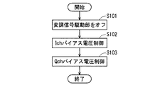
図2は、本実施の形態における光送信器のバイアス電圧制御方法のフローチャートである。また、図3は、図2におけるステップS102の詳細なフローチャートである。つまり、図3は、第1の光変調器101のバイアス電圧(即ちIchバイアス電圧)制御方法のフローチャートである。
FIG. 2 is a flowchart of the bias voltage control method of the optical transmitter in this embodiment. FIG. 3 is a detailed flowchart of step S102 in FIG. That is, FIG. 3 is a flowchart of the bias voltage (ie, Ich bias voltage) control method for the first
光源1が立ち上がり、正常な光レベルの光が光変調部100に入力されるようになった後、制御部200は初期値探索を開始する。なお、初期値探索を行う前は、収束点が全く分からない。まず、制御部200は、初期状態として変調信号駆動部2をオフする(ステップS101)。つまり、初期値探索の開始状態として、同期検波部201は変調信号駆動部2から第1、第2の光変調器101,102にアナログ変調信号が入力しないようにする。
After the light source 1 is activated and light having a normal light level is input to the
本明細書では、第1、第2の光変調器101,102、光位相調整部103のそれぞれに印加するバイアス電圧を、Ichバイアス電圧、Qchバイアス電圧、PSバイアス電圧と記載する。また、第1、第2の光変調器101,102のそれぞれから出力される出力光を、Ich光、Qch光と記載する。合波された出力光(即ち光変調部100の出力光)を合成光と記載する。なお、本実施の形態では第1の光変調器101にIchを割り当て、第2の光変調器102にQchを割り当てたが、それぞれ逆のチャネルを割り当てても良い。
In this specification, the bias voltage applied to each of the first and second
次に、ステップS102において、制御部200はIchバイアス電圧の初期値探索を行う。なお、図2のステップS102(即ち図3のステップS1011〜S1015)において、Qchバイアス電圧とPSバイアス電圧は任意の一定値とする。光変調部100の合成光のレベルをモニタするため、モニタ部204は電流電圧変換部3から出力される電圧信号をモニタする。同期検波部201はモニタ部204がモニタする電圧信号に基づいて、光変調部100の合成光の強度が最大となるIchバイアス電圧を探索してVi1とする(ステップS1011)。次に同期検波部201は、Ichバイアス電圧を変動させ、Vi1に最も近く(即ちVi1に隣接し)、かつ、光変調部100の合成光の強度が極大になるIchバイアス電圧を探索してVi2とする(ステップS1012)。
Next, in step S102, the
次に、Vi1とVi2の差が、所定の閾値(例えば1.2Vπ)よりも小さいか否かの判定を行う(ステップS1013)。Vi1とVi2の差が閾値よりも小さい場合は、Vi1とVi2を加算して2で割った値を、第1の光変調器101における初期バイアス電圧Viとして設定して(ステップS1015)、Ichバイアス電圧制御を終了する。 Next, it is determined whether or not the difference between Vi1 and Vi2 is smaller than a predetermined threshold (for example, 1.2 Vπ) (step S1013). If the difference between Vi1 and Vi2 is smaller than the threshold, a value obtained by adding Vi1 and Vi2 and dividing by 2 is set as the initial bias voltage Vi in the first optical modulator 101 (step S1015), and the Ich bias End voltage control.
一方、Vi1とVi2の差が閾値よりも大きい場合は、ステップS1014に進む。ステップS1014において、Qchバイアス電圧もしくはPSバイアス電圧の値を変更して、ステップS1011に戻り、Ichバイアス電圧の初期値探索を繰り返す。なお、ステップS1013においてVi1とVi2の差を閾値と比較する理由は後述する。 On the other hand, if the difference between Vi1 and Vi2 is greater than the threshold, the process proceeds to step S1014. In step S1014, the value of the Qch bias voltage or PS bias voltage is changed, and the process returns to step S1011 to repeat the initial value search for the Ich bias voltage. The reason for comparing the difference between Vi1 and Vi2 with the threshold in step S1013 will be described later.
以上で、図2のステップS102が終了した。次に、図2のステップS103の説明を行う。ステップS103は、第1の光変調器101にステップS102において求めた初期バイアス電圧Viを印加した状態で行う。この状態において、Ich光は消光状態となっているので、光変調部100から出力される合成光は、Qch光とみなすことができる。そこで、ステップS103においては、Qch光が消光状態となるQchバイアス電圧を見つけるために、光変調部100から出力される合成光が消光となるQchバイアス電圧を探索する。探索したQchバイアス電圧を第2の光変調器102における初期バイアス電圧Vqとして設定する。
This completes step S102 of FIG. Next, step S103 in FIG. 2 will be described. Step S103 is performed in a state where the initial bias voltage Vi obtained in step S102 is applied to the first
以上により、初期値探索が終了する。通常状態においては、第1、第2の光変調器101,102に印加するバイアス電圧として、それぞれ初期バイアス電圧Vi、Vqを設定する。そして、変調信号駆動部2をオンして、アナログ変調信号が第1、第2の光変調器101,102にそれぞれ入力される。これにより光変調部100は変調の状態となる。
Thus, the initial value search ends. In the normal state, initial bias voltages Vi and Vq are set as bias voltages applied to the first and second
以下では、図3のステップS1013において、Vi1とVi2の差を閾値と比較する理由を説明する。 Hereinafter, the reason why the difference between Vi1 and Vi2 is compared with the threshold value in step S1013 of FIG. 3 will be described.
まず、図4(a)〜(d)を用いて、Ich光とQch光の間に位相差がある場合について説明する。図4(a)〜(c)は、Qchバイアス電圧およびPSバイアス電圧を固定したままでIchバイアス電圧を変化させた時の、Ich光、Qch光および合成光の光ベクトル(図4(a))、合成光の強度(図4(b))、Ich光の強度(図4(c))である。図中の矢印、点線はそれぞれ対応している。 First, a case where there is a phase difference between Ich light and Qch light will be described with reference to FIGS. 4A to 4C show optical vectors of the Ich light, the Qch light, and the combined light when the Ich bias voltage is changed while the Qch bias voltage and the PS bias voltage are fixed (FIG. 4A). ), The intensity of the synthesized light (FIG. 4B), and the intensity of the Ich light (FIG. 4C). The arrows and dotted lines in the figure correspond to each other.
図4(a)および図4(b)より、Ichバイアス電圧がVi1の時には、Ich光の光ベクトルの大きさは最大になり、合成光の強度も最大になる。また、Ichバイアス電圧がVi2の時には、Ich光の光ベクトルは、Ichバイアス電圧がVi1の時と逆方向を向く。また、合成光の強度は極大となる。図4(c)に示すように、Ich光の光ベクトルは、Ichバイアス電圧に対して正弦波の振る舞いを示す。すなわち、図4(c)に示すように、Ichバイアス電圧として、Vi1とVi2のちょうど中間のバイアス電圧を印加する時、Ich光は消光状態(Null点)となる。Ich光が消光状態となっている場合、光変調部100から出力される合成光はQch光となる(図4(d))。
4A and 4B, when the Ich bias voltage is Vi1, the magnitude of the optical vector of the Ich light is maximized, and the intensity of the combined light is also maximized. When the Ich bias voltage is Vi2, the optical vector of the Ich light is in the opposite direction to that when the Ich bias voltage is Vi1. In addition, the intensity of the synthesized light is maximized. As shown in FIG. 4C, the optical vector of the Ich light exhibits a sine wave behavior with respect to the Ich bias voltage. That is, as shown in FIG. 4C, when a bias voltage that is exactly halfway between Vi1 and Vi2 is applied as the Ich bias voltage, the Ich light is in the extinction state (Null point). When the Ich light is in the extinction state, the combined light output from the
次に、図5(a)〜(c)を用いて、Ich光とQch光の間に位相差が無い場合について説明する。図5(a)〜(c)は、Qchバイアス電圧およびPSバイアス電圧を固定したままでIchバイアス電圧を変化させた時の、Ich光、Qch光および合成光の光ベクトル(図5(a))、合成光の強度(図5(b))、Ich光の強度(図5(c))である。 Next, a case where there is no phase difference between the Ich light and the Qch light will be described with reference to FIGS. FIGS. 5A to 5C show optical vectors of Ich light, Qch light, and combined light when the Ich bias voltage is changed while the Qch bias voltage and the PS bias voltage are fixed (FIG. 5A). ), The intensity of the synthesized light (FIG. 5B), and the intensity of the Ich light (FIG. 5C).
図5(a)および図5(b)から、Qch光の強度が最大の場合、図4(b)の様な極大点を感知することはできず、誤ったバイアス電圧をVi2として設定してしまう。この時、Ichバイアス電圧としてVi1を印加した場合のIch光と、Vi2を印加した場合のIch光の状態は同じである。そのため、Vi1とVi2のちょうど中間のバイアス電圧をIchバイアス電圧の初期値として設定しても、Ich光は消光状態にならない。よって、この場合、Vi2を誤って設定することにより、誤った初期バイアス電圧Viを設定してしまう。 From FIG. 5A and FIG. 5B, when the intensity of the Qch light is maximum, the local maximum point as in FIG. 4B cannot be detected, and an incorrect bias voltage is set as Vi2. End up. At this time, the state of the Ich light when Vi1 is applied as the Ich bias voltage and the state of the Ich light when Vi2 is applied are the same. For this reason, even if a bias voltage just in the middle of Vi1 and Vi2 is set as the initial value of the Ich bias voltage, the Ich light does not enter the extinction state. Therefore, in this case, setting Vi2 incorrectly sets the initial bias voltage Vi incorrectly.
上述した初期値の誤りは、Ich光とQch光が同相もしくは逆相、かつ、Qch光の強度が最大の条件の時にのみ発生する。図3のステップS1013を設けるのは、この初期値の誤りを防止するためである。ステップS1012においてVi2が正しく設定された場合、Vi1とVi2の差はVπ(変調器毎に定められる半波長電圧)となる(図4(b))。一方、Vi2が誤って設定された場合、Vi1とVi2の差は2Vπとなる(図5(b))。そこで、ステップS1013において、予め閾値を設定しておき、Vi1とVi2の差の絶対値が設定した閾値よりも小さいか否かを判断することで、Vi2が誤って設定されることを防止する。閾値は与えられた第1の光変調器101のVπを元に、Vπより大きく、かつVπの2倍より小さい値の範囲で適宜設定すればよく、例えば、Vπの1.2倍(1.2Vπ)としてもよい。
The initial value error described above occurs only when the Ich light and Qch light are in phase or reverse phase and the intensity of the Qch light is maximum. The reason for providing step S1013 in FIG. 3 is to prevent an error in the initial value. When Vi2 is set correctly in step S1012, the difference between Vi1 and Vi2 is Vπ (half wavelength voltage determined for each modulator) (FIG. 4B). On the other hand, when Vi2 is set incorrectly, the difference between Vi1 and Vi2 is 2Vπ (FIG. 5B). Therefore, in step S1013, a threshold value is set in advance, and it is determined whether the absolute value of the difference between Vi1 and Vi2 is smaller than the set threshold value, thereby preventing Vi2 from being set erroneously. The threshold value may be set as appropriate within a range of values larger than Vπ and smaller than twice Vπ based on the given Vπ of the first
従来は、Ichバイアス電圧、Qchバイアス電圧、PSバイアス電圧のそれぞれを2Vπの範囲で変動させて、光変調部100からの光出力をモニタしていた。例えば、それぞれのバイアス電圧を32通りずつ変えながらモニタを行うと、モニタ点の組合せは32×32×32=32768通りになる。本実施の形態の方法では、例えば、Ichバイアス電圧を4Vπの範囲で256通りに変化させ、Ichバイアス電圧の初期値が決定した後、Qchバイアス電圧を4Vπの範囲で256通りに変化させるとする。本実施の形態では、片方のバイアス電圧を制御する際は、もう片方のバイアス電圧を固定しているため、256+256=512通りのバイアス電圧の組合せをモニタすれば、Ichバイアス電圧およびQchバイアス電圧の初期値を決定することが可能である。つまり、より高速に初期値探索を完了することができる。
Conventionally, each of the Ich bias voltage, the Qch bias voltage, and the PS bias voltage is varied within a range of 2Vπ to monitor the light output from the
<効果>
本実施の形態における光送信器は、入射光を変調する光変調部100と、光変調部100に変調信号を入力する変調信号駆動部2と、光変調部100および変調信号駆動部2を制御する制御部200と、を備える光送信器であって、光変調部100は、光源1から入射した光を2つの光に分岐する分岐部106aと、印加されたバイアス電圧および入力された変調信号に基づいて2つの光のそれぞれを変調するマッハツェンダ型の2つの光変調器(第1、第2の光変調器101,102)と、2つの光変調器のいずれかに接続され、印加されたバイアス電圧に基づいて光変調器に入射する光の位相を調整する光位相調整部103と、2つの光変調器からの出力光を合波して出力する合波部106bと、合波部106bから出力される光の強度を検出する光強度検出部104と、を備え、変調信号駆動部2は、2つの光変調器の各々に変調信号を入力し、制御部200は、変調信号が入力されない状態としての初期状態において2つの光変調器に印加されるバイアス電圧を探索して決定する制御部200であって、制御部200は、2つの光変調器の各々に変調信号が入力されない状態において、2つの光変調器のうち一方の光変調器(第2の光変調器102)および光位相調整部103に印加するバイアス電圧を一定に保ちながら、光強度検出部104が検出する光の強度に基づいて、2つの光変調器のうち他方の光変調器(第1の光変調器101)からの出力光がゼロになるように、当該他方の光変調器に印加するバイアス電圧を第1初期バイアス電圧(即ち、第1の光変調器101に印加する初期バイアス電圧Vi)として決定し、その後に、当該他方の光変調器に第1初期バイアス電圧を印加し、かつ、光位相調整部103に印加するバイアス電圧を一定に保ちながら、光強度検出部104が検出する光の強度に基づいて、一方の光変調器からの出力光がゼロになるように、当該一方の光変調器に印加するバイアス電圧を第2初期バイアス電圧(即ち、第2の光変調器102に印加する初期バイアス電圧Vq)として決定することを特徴とする。
<Effect>
The optical transmitter according to the present embodiment controls an
従って、本実施の形態の光送信器は、第1の光変調器101の初期バイアス電圧Viを探索する際には、第2の光変調器102および光位相調整部103に印加するバイアス電圧を一定値に固定する。そして、第1の光変調器101の初期バイアス電圧Viを決定した後に、第2の光変調器102の初期バイアス電圧Vqを探索する際には、第1の光変調器101および光位相調整部103に印加するバイアス電圧の値を一定値に固定する。よって、本実施の形態における光送信器は、第1、第2の光変調器101,102のバイアス電圧を同時に変化させながら探索を行うのではなく、一方の光変調器のバイアス電圧を固定した状態で他方の光変調器のバイアス電圧の探索を行うため、より高速に初期バイアス電圧の探索を完了することが可能である。
Therefore, when searching for the initial bias voltage Vi of the first
また、本実施の形態における光送信器において、制御部200は、他方の光変調器(第1の光変調器101)に印加するバイアス電圧を変化させることにより、光強度検出部104が検出する光の強度が最大となるバイアス電圧(Vi1)と、バイアス電圧(Vi1)に隣接し、かつ光強度検出部104が検出する光の強度が極大となるバイアス電圧(Vi2)とを探索し、2つのバイアス電圧(Vi1、Vi2)を加算して2で割った値を、他方の光変調器(第1の光変調器101)からの出力光がゼロになる第1初期バイアス電圧(即ち初期バイアス電圧Vi)として決定することを特徴とする。
In the optical transmitter according to the present embodiment, the
従って、一方の光変調器(第2の光変調器102)および光位相調整部103のバイアス電圧を固定した状態において、他方の光変調器(第1の光変調器101)のバイアス電圧の制御を行うことによって、第1の光変調器101から光が出力しない状態にすることが可能である。まず、第1の光変調器101から光が出力しない状態にすることにより、その後、第2の光変調器102のバイアス電圧の制御を容易に行うことが可能となる。
Therefore, in a state where the bias voltage of one optical modulator (second optical modulator 102) and the optical
また、本実施の形態における光送信器において、制御部200は、2つのバイアス電圧(即ちVi1とVi2)の差が予め定められた閾値を超える場合、一方の光変調器(第2の光変調器102)または光位相調整部103に印加するバイアス電圧を変更して探索をやり直すことを特徴とする。
In the optical transmitter according to the present embodiment, when the difference between the two bias voltages (that is, Vi1 and Vi2) exceeds a predetermined threshold value, the
従って、Vi1とVi2の差が2Vπとなる場合、初期バイアス電圧Viを誤った値に設定してしまう。これを避けるために、Vi1とVi2の差が例えば1.2Vπを超えるか否かを調べて、超える場合は探索をやり直すことで、初期バイアス電圧Viを正しい値に設定することが可能となる。 Therefore, when the difference between Vi1 and Vi2 is 2Vπ, the initial bias voltage Vi is set to an incorrect value. In order to avoid this, it is possible to set the initial bias voltage Vi to a correct value by investigating whether or not the difference between Vi1 and Vi2 exceeds 1.2Vπ, for example.
また、本実施の形態における光送信器において、所定の閾値は、他方の光変調器(第1の光変調器101)において定められたπシフト電圧より大きく、かつπシフト電圧の2倍よりも小さい値である。 In the optical transmitter according to the present embodiment, the predetermined threshold is greater than the π shift voltage determined in the other optical modulator (first optical modulator 101) and more than twice the π shift voltage. Small value.
従って、初期バイアス電圧が正しく設定される場合は、Vi1とVi2の差はVπとなる。一方、初期バイアス電圧が誤って設定される場合は、Vi1とVi2の差は2Vπとなる。よって、閾値をVπと2Vπの間の点、例えば1.2Vπとすることで、初期バイアス電圧Viが正しく設定されているか否かを判別することが可能である。 Therefore, when the initial bias voltage is set correctly, the difference between Vi1 and Vi2 is Vπ. On the other hand, if the initial bias voltage is set incorrectly, the difference between Vi1 and Vi2 is 2Vπ. Therefore, by setting the threshold value to a point between Vπ and 2Vπ, for example, 1.2Vπ, it is possible to determine whether or not the initial bias voltage Vi is set correctly.
また、本実施の形態における光送信器に制御方法は、入射光を変調する光変調部100と、光変調部100に変調信号を入力する変調信号駆動部2と、光変調部100および変調信号駆動部2を制御する制御部200と、を備える光送信器の制御方法であって、光変調部100は、光源1から入射した光を2つの光に分岐する分岐部106aと、印加されたバイアス電圧および入力された変調信号に基づいて2つの光のそれぞれを変調するマッハツェンダ型の2つの光変調器(第1、第2の光変調器101,102)と、2つの光変調器のいずれかに接続され、印加されたバイアス電圧に基づいて当該光変調器に入射する光の位相を調整する光位相調整部103と、2つの光変調器からの出力光を合波して出力する合波部106bと、合波部106bから出力される光の強度を検出する光強度検出部104と、を備え、変調信号駆動部2は、2つの光変調器(第1、第2の光変調器101,102)の各々に変調信号を入力し、(a)制御部200が、2つの光変調器に入力される変調信号をオフする工程と、(b)工程(a)の後、制御部200が、2つの光変調器のうち一方の光変調器(第2の光変調器102)および光位相調整部103に印加するバイアス電圧を一定に保つ工程と、(c)工程(b)の後、制御部200が、光強度検出部104が検出する光の強度に基づいて、2つの光変調器のうち他方の光変調器(第1の光変調器101)からの出力光がゼロになるように、当該他方の光変調器に印加するバイアス電圧を第1初期バイアス電圧(即ち、第1の光変調器101に印加する初期バイアス電圧Vi)として決定する工程と、(d)工程(c)の後、制御部200が、他方の光変調器(第1の光変調器101)に第1初期バイアス電圧を印加し、かつ、光位相調整部103に印加するバイアス電圧を一定に保ちながら、光強度検出部104が検出する光の強度に基づいて、一方の光変調器(第2の光変調器102)からの出力光がゼロになるように、当該一方の光変調器に印加するバイアス電圧を第2初期バイアス電圧(即ち、第2の光変調器102に印加する初期バイアス電圧Vq)として決定する工程と、を備える。
The control method for the optical transmitter according to the present embodiment includes an
従って、本実施の形態における光送信器の制御方法は、第1の光変調器101の初期バイアス電圧Viを探索する際には、第2の光変調器102および光位相調整部103に印加するバイアス電圧を一定値に固定する。そして、第1の光変調器101の初期バイアス電圧Viを決定した後に、第2の光変調器102の初期バイアス電圧Vqを探索する際には、第1の光変調器101および光位相調整部103に印加するバイアス電圧の値を一定値に固定する。よって、本実施の形態における光送信器の制御方法は、第1、第2の光変調器101,102のバイアス電圧を同時に変化させながら探索を行うのではなく、一方の光変調器のバイアス電圧を固定した状態で他方の光変調器のバイアス電圧の探索を行うため、より高速に初期バイアス電圧の探索を完了することが可能である。
Therefore, in the control method of the optical transmitter in the present embodiment, when searching for the initial bias voltage Vi of the first
<実施の形態2>
<構成>
実施の形態1における光送信器は、変調信号が光変調部100に入力していない初期状態において、光変調部100の出力をモニタし、光変調部100から出力される光が最も消光状態となるように、第1、第2の光変調器101,102の初期バイアス電圧を探索した。本実施の形態における光送信器は、実施の形態1と同様に、変調信号が光変調部100に入力していない初期状態において、光変調部100から出力される光が最も消光状態となるようにIchバイアス電圧およびQchバイアス電圧の初期値(初期バイアス電圧Vi、Vq)を探索する。
<
<Configuration>
The optical transmitter according to the first embodiment monitors the output of the
図6は、本実施の形態における光送信器の機能ブロック図である。本実施の形態における光送信器は、実施の形態1における光送信器(図1)に対して、低周波信号生成部203a,203bをさらに備える。低周波信号生成部203aは、加算部205aを介してIchバイアス電圧に低周波信号を重畳する。同様に、低周波信号生成部203bは、加算部205bを介してQchバイアス電圧に低周波信号を重畳する。その他の構成は実施の形態1(図1)と同じため説明を省略する。
FIG. 6 is a functional block diagram of the optical transmitter according to the present embodiment. The optical transmitter according to the present embodiment further includes low
<動作>
実施の形態1で用いたフローチャート(図2および図3)を用いて、本実施の形態における光送信器のバイアス電圧制御方法を説明する。図3におけるステップS101は実施の形態1と同様のため、説明を省略する。図3を用いて、図2のステップS102の説明を行う。図2のステップS102においては、低周波信号生成部203aをオンして、加算部205aにてバイアス印加部202aから出力されたIchバイアス電圧に低周波の微小信号を重畳する。なお、ステップS102において低周波信号生成部203bはオフ状態とする。
<Operation>
The bias voltage control method for the optical transmitter in the present embodiment will be described using the flowcharts (FIGS. 2 and 3) used in the first embodiment. Step S101 in FIG. 3 is the same as that in the first embodiment, and a description thereof will be omitted. The step S102 in FIG. 2 will be described with reference to FIG. In step S102 of FIG. 2, the low frequency
まず、図3のステップS1011において、実施の形態1と同様、合成光が最大となるIchバイアス電圧を探索して、これをVi1とする。制御部200は、光変調部100から出力される合成光を光強度検出部104で得る。さらに電流電圧変換部3を通し、モニタ部204で微小変調信号成分のモニタを行う。モニタ部204は電流電圧変換部3から出力される電気信号を、ADCを用いてアナログ信号からデジタル信号に変換してモニタする。もしくは、モニタ部204は電流電圧変換部3から出力された電圧信号に含まれる低周波信号としての低周波の微小変調信号をモニタする。この時、微小変調信号成分の時間平均値は、光出力が極大、もしくは極小の時に0となる。つまり、ステップS1011において、同期検波部201は、低周波信号をIchバイアス電圧に重畳しながらIchバイアス電圧を変化させる。その応答として、光出力の時間平均値を同期検波部201にフィードバックし、時間平均値が0となるようにIchバイアス電圧を決定する。この時間平均の周期は、例えば低周波信号生成部で出力される低周波の周期と同じでも良い。また、この、光出力から得た微小変調信号成分の時間平均値のことを誤差信号と呼ぶ。すなわち、誤差信号が0となるIchバイアス電圧の探索を行い、このIchバイアス電圧の値をVi1とする。
First, in step S1011 in FIG. 3, as in the first embodiment, an Ich bias voltage that maximizes the combined light is searched for and set to Vi1. The
次に、図3のステップS1012において、実施の形態1と同様、Vi1に隣接し、かつ合成光が極大となるIchバイアス電圧を探索して、これをVi2とする。合成光が極大となるのは、誤差信号が0のときである。よって、誤差信号が0となるようにIchバイアス電圧を決定する。 Next, in step S1012 of FIG. 3, as in the first embodiment, an Ich bias voltage that is adjacent to Vi1 and has the maximum combined light is searched for and set to Vi2. The combined light becomes maximum when the error signal is zero. Therefore, the Ich bias voltage is determined so that the error signal becomes zero.
図3における以降のステップS1013〜S1014は実施の形態1と同じため、説明を省略する。 Since subsequent steps S1013 to S1014 in FIG. 3 are the same as those in the first embodiment, description thereof will be omitted.
図2のステップS102終了後、一定時間が経過した後、ステップS103に進む。ステップS103では、Qchバイアス電圧の初期値探索を行う。まず、低周波信号生成部203aをオフにして、低周波信号生成部203bをオンにする。なお、PSバイアス電圧は一定値に固定し、Ichバイアス電圧はViに固定する。つまり、Qchバイアス電圧にのみ、低周波の微小信号が重畳される。そして、光変調部100から出力される合成光が最も消光となるように、Qchバイアス電圧の探索を行い、これを初期バイアス電圧Vqと決定する。以上により、初期値探索が終了する。
After the completion of step S102 in FIG. 2, the process proceeds to step S103 after a predetermined time has elapsed. In step S103, an initial value search for the Qch bias voltage is performed. First, the low
<効果>
本実施の形態における光送信器において、制御部200は、2つの光変調器(第1、第2の光変調器101,102)に印加されるバイアス電圧のそれぞれに低周波信号を重畳する低周波信号生成部203a,203bをさらに備えることを特徴とする。
<Effect>
In the optical transmitter according to the present embodiment, the
従って、Ichバイアス電圧に低周波信号を重畳し、合成光の誤差信号に基づいて初期バイアス電圧Viを決定することで、より精度良く初期バイアス電圧Viを探索することが可能である。同様に、Qchバイアス電圧に低周波信号を重畳し、合成光の誤差信号に基づいて初期バイアス電圧Vqを決定することで、より精度良く初期バイアス電圧Vqを探索することが可能である。 Therefore, it is possible to search for the initial bias voltage Vi with higher accuracy by superimposing the low frequency signal on the Ich bias voltage and determining the initial bias voltage Vi based on the error signal of the combined light. Similarly, it is possible to search the initial bias voltage Vq with higher accuracy by superimposing a low-frequency signal on the Qch bias voltage and determining the initial bias voltage Vq based on the error signal of the combined light.
<実施の形態3>
<構成>
実施の形態1および実施の形態2における光送信器は、変調信号が光変調部100に入力していない初期状態において、光変調部100の出力をモニタし、光変調部100から出力される光が最も消光状態となるように、第1、第2の光変調器101,102の初期バイアス電圧Vi、Vqを探索した。
<Embodiment 3>
<Configuration>
The optical transmitters in the first embodiment and the second embodiment monitor the output of the
本実施の形態における光送信器は、実施の形態1および実施の形態2と同様に、変調信号が光変調部100に入力していない初期状態において、光変調部100から出力される光が最も消光状態となるように初期バイアス電圧Vi、Vqを探索する。本実施の形態では、まず、PSバイアス電圧を決定し、その後でIchバイアス電圧およびQchバイアス電圧の初期値を探索する点が、実施の形態1および実施の形態2と異なる。本実施の形態における光送信器は、実施の形態2における光送信器(図6)と同じ構成のため、光送信器の構成に関する説明を省略する。
In the optical transmitter according to the present embodiment, the light output from the
<動作>
図7は、本実施の形態における光送信器のバイアス電圧制御方法のフローチャートである。光源1が立ち上がり、正常な光レベルが光変調部100に入力されるようになった後、制御部200は初期値探索を開始する。なお、初期値探索を行う前は、収束点が全く分からない。まず、制御部200は、初期状態として変調信号駆動部2をオフする(ステップS201)。つまり、初期値探索の開始状態として、同期検波部201は変調信号駆動部2から第1、第2の光変調器101,102にアナログ変調信号が入力しないようにする。
<Operation>
FIG. 7 is a flowchart of the bias voltage control method of the optical transmitter in this embodiment. After the light source 1 is activated and a normal light level is input to the
次に、ステップS202においてPSバイアス電圧の制御を行う。まず、制御部200は、低周波信号生成部203aをオンして、Ichバイアス電圧に低周波信号を重畳する。さらに、制御部200は、低周波信号生成部203bをオンして、Ichバイアス電圧に重畳した低周波信号からπ/2位相をシフトさせた低周波信号をQchバイアス電圧に重畳する。同期検波部201は、モニタ部204が検出する誤差信号が0になるようにPSバイアス電圧のフィードバック制御を行い、このPSバイアス電圧をVpsとして決定する。
Next, in step S202, the PS bias voltage is controlled. First, the
この状態において、Ich光とQch光との位相差は、π/2か、−π/2のどちらかの状態となる。すなわち、この時、Ich光とQch光は互いに独立の関係となる。ゆえに、独立の状態において、例えば、Qchバイアス電圧を固定し、Ichバイアス電圧のみを変動させた時の光変調部100からの出力光の変動分は、Ich光の変動分を示すことになる。このため、以降のステップS203,S204においてIchバイアス電圧およびQchバイアス電圧の初期値探索を行う際に、光変調部100からの合成光をモニタしながら、第1、第2の光変調器101,102の出力光の制御を独立に行うことが可能になる。
In this state, the phase difference between the Ich light and the Qch light is either π / 2 or −π / 2. In other words, at this time, the Ich light and the Qch light are independent of each other. Therefore, in an independent state, for example, when the Qch bias voltage is fixed and only the Ich bias voltage is changed, the fluctuation amount of the output light from the
次に、ステップS203においてIchバイアス電圧の初期値探索を行う。まず、低周波信号生成部203aはオンのまま、低周波信号生成部203bをオフにする。また、PSバイアス電圧はVpsに固定する。つまり、Ichバイアス電圧にのみ、低周波の微小信号が重畳される。そして、光変調部100から出力される合成光が最も消光となるように、Ichバイアス電圧の探索を行い、これを初期バイアス電圧Viと決定する。
Next, in step S203, an initial value search for the Ich bias voltage is performed. First, the low frequency
ステップS203終了後、一定時間が経過した後、ステップS203に進む。ステップS203では、Qchバイアス電圧の初期値探索を行う。まず、低周波信号生成部203aをオフにして、低周波信号生成部203bをオンにする。なお、PSバイアス電圧はVpsに固定し、Ichバイアス電圧はViに固定する。つまり、Qchバイアス電圧にのみ、低周波の微小信号が重畳される。そして、光変調部100から出力される合成光が最も消光となるように、Qchバイアス電圧の探索を行い、これを初期バイアス電圧Vqと決定する。
After the end of step S203, after a predetermined time has passed, the process proceeds to step S203. In step S203, an initial value search for the Qch bias voltage is performed. First, the low
以上で、光位相調整部103、第1、第2の光変調器101,102に印加する初期バイアス電圧Vps、Vi、Vqが決定されたので、初期値探索を終了する。通常状態においては、Ichバイアス電圧、Qchバイアス電圧の初期値として、それぞれVi、Vqを設定する。そして、変調信号駆動部2をオンして、アナログ変調信号が第1、第2の光変調器101,102にそれぞれ入力される。これにより光変調部100は変調の状態となる。
As described above, since the initial bias voltages Vps, Vi, and Vq to be applied to the optical
<効果>
本実施の形態における光送信器において、制御部200は、2つの光変調器(第1、第2の光変調器101,102)からの出力光の位相差がπ/2となるように光位相調整部103に印加するバイアス電圧を決定し、光位相調整部103に決定した当該バイアス電圧を印加しながら、第1、第2の初期バイアス電圧(即ち、第1の光変調器101に印加する初期バイアス電圧Viと、第2の光変調器102に印加する初期バイアス電圧Vq)を決定することを特徴とする。
<Effect>
In the optical transmitter according to the present embodiment, the
従って、初期値探索において、まず、第1、第2の光変調器101,102からの出力光の位相差がπ/2となるように光位相調整部103に印加するバイアス電圧(PSバイアス電圧)を調整する。これにより、第1、第2の光変調器101,102からの出力光が互いに直交した状態となり、第1、第2の光変調器101,102のバイアス電圧を独立に制御することが可能となる。
Therefore, in the initial value search, first, a bias voltage (PS bias voltage) applied to the optical
また、本実施の形態における光送信器において、制御部200は、2つの光変調器(第1、第2の光変調器101,102)のそれぞれに印加するバイアス電圧に低周波信号をそれぞれ重畳した後、2つの光変調器からの出力光の位相差がπ/2となるように光位相調整部103に印加するバイアス電圧を決定することを特徴とする。
In the optical transmitter according to the present embodiment, the
従って、第1、第2の光変調器101,102に印加するバイアス電圧に低周波信号をそれぞれ重畳してから、光位相調整部103に印加するバイアス電圧(PSバイアス電圧)を調整することにより、高速に位相差をπ/2にすることが可能である。
Therefore, by adjusting the bias voltage (PS bias voltage) applied to the optical
<実施の形態4>
実施の形態3における光送信器は、変調信号が光変調部100に入力していない初期状態として、光変調部100から出力される合成光をモニタし、光変調部100から出力される合成光が最も消光状態となるように、初期バイアス電圧を探索する。
<Embodiment 4>
The optical transmitter according to the third embodiment monitors the combined light output from the
本実施の形態における光送信器は、実施の形態3と同様に、変調信号が光変調部100に入力していない初期状態に、光変調部100から出力される光が最も消光状態となるようにPSバイアス電圧、Ichバイアス電圧、Qchバイアス電圧の順に初期バイアス電圧Vps、Vi、Vqを探索するようにしたものである。本実施の形態における光送信器は、実施の形態2とはPSバイアス電圧の探索方法が異なる。
As in the third embodiment, the optical transmitter according to the present embodiment is configured so that the light output from the
<構成>
図8は、本実施の形態における光送信器のブロック図である。図8において、実施の形態2および実施の形態3(図6)からの追加部分は、低周波信号生成部203cおよび加算部205cである。低周波信号生成部203cは、加算部205cを介して、光位相調整部103に印加されるPSバイアス電圧に低周波信号を重畳する。その他の構成は実施の形態2および実施の形態3と同じため、説明を省略する。
<Configuration>
FIG. 8 is a block diagram of the optical transmitter according to the present embodiment. In FIG. 8, the additional portions from the second embodiment and the third embodiment (FIG. 6) are a low-frequency
<動作>
次に動作について説明する。光強度検出部104からの光強度に応じた電流信号は電流電圧変換部3にて電圧信号に変換され、この出力された電圧信号は制御部200内のモニタ部204に入力され、モニタ部204は電流電圧変換部3から出力された電圧信号に含まれる低周波信号としての低周波の微小変調信号をモニタする。同期検波部201はモニタ部を介して同期検波部201に入力された電圧信号から誤差信号を抽出し、この誤差信号が0となるようなバイアス電圧を演算により求める。バイアス印加部202a、202b、202cは、モニタ部204を介して同期検波部201で抽出された誤差信号に基づくバイアス電圧を出力する。
<Operation>
Next, the operation will be described. The current signal corresponding to the light intensity from the light
バイアス印加部202a、202b、202cからの出力が、低周波信号生成部203a、203b、203cからの低周波信号としての微小変調信号と加算部205a、205b、205cで加算され、第1、第2の光変調器101,102、光位相調整部103にそれぞれ入力される。
Outputs from the
また、図8において、同期検波部201内での処理はデジタル信号処理のため、モニタ部204は、ADC(Analog−to−Digital Converter)を用いて、入力された電圧信号をアナログ信号からデジタル信号に変換してモニタする。同様に、バイアス印加部202a、202b、202cは、DAC(Digital−to−Analog Converter)を用いてデジタル信号からアナログ信号に変換したバイアス電圧を出力する。同期検波部201は、第1、第2の光変調器101,102および光位相調整部103に対する各バイアスの制御を独立に、時系列で行う。その手順については後述する。
In FIG. 8, since the processing in the
図7は、本実施の形態における光送信器のバイアス電圧制御方法のフローチャートである。また、図9は、図7におけるステップS202の詳細なフローチャートである。つまり、図9は、光位相調整部103のバイアス電圧の初期値探索方法のフローチャートである。
FIG. 7 is a flowchart of the bias voltage control method of the optical transmitter in this embodiment. FIG. 9 is a detailed flowchart of step S202 in FIG. That is, FIG. 9 is a flowchart of a method for searching for an initial value of the bias voltage of the optical
光源1が立ち上がり正常な光レベルが光変調部100に入力されるようになった後、制御部200は、バイアス制御を開始する。なお、バイアス制御の立ち上げ前には、収束点が全く分からない。
After the light source 1 is turned on and a normal light level is input to the
まず、初期値探索の開始状態として、同期検波部201は、変調信号駆動部2から第1、第2の光変調器101,102にアナログ変調信号が入力しないようにする。すなわち変調信号駆動部2はオフの状態で開始する(図7のステップS201)。
First, as an initial value search start state, the
次に、図7のステップS102において、同期検波部201はPSバイアス電圧の初期値探索を行う。同期検波部201は、低周波信号生成部203cをオンし、光位相調整部103に印加されるバイアスに低周波の微小信号を重畳する。
Next, in step S102 in FIG. 7, the
そして、光変調部100から出力される合成光の強度が最大になるように、光位相調整部103に印加するバイアス電圧を制御する。この制御時に決定したバイアス印加部202cから出力するPSバイアス電圧をVps1と定義する(図9のステップS2011)。
Then, the bias voltage applied to the optical
一定時間経過後、光位相調整部103に印加されるバイアス電圧に低周波の微小信号を重畳させたまま、光変調部100から出力される合成光の強度が最も消光となるように、光位相調整部に印加するバイアス電圧の制御を行う。この制御時に決定したバイアス印加部202cから出力するPSバイアス電圧をVps2と定義する(図9のステップS2012)。なお、Vps2はVps1に隣接するように決定される。
After a certain period of time, the optical phase is adjusted so that the intensity of the combined light output from the
前述のように、光位相調整部103は第1、第2の光変調器101,102からの出力光の位相差を制御する。光位相調整部103の制御によって光変調部100から出力される合成光の強度が最大の時、第1、第2の光変調器101,102から出力される光は同位相となる。一方、光変調部100から出力される合成光が消光状態の時、第1、第2の光変調器101,102から出力される光は逆位相となる。
As described above, the optical
なお、ステップS2011の制御を開始した時点で、第1の光変調器101および第2の光変調器102からの光出力が消光状態であると、光位相調整部103でバイアス制御を実施しても、光変調部100から出力される合成光の強度が最大となるバイアス電圧へと制御できない。
When the light output from the first
このため、ステップS2011,S2012において決定したPSバイアス電圧Vps1,Vps2の2つのバイアス電圧の差が第1、第2の光変調器101,102で設定されているVπから大きく外れているかどうかの判定を行う(図9のステップS2013)。つまり、ステップS2013において、2つのバイアス電圧Vps1とVps2の差が予め定めた閾値(例えばVπの1.3倍)よりも小さいか否かの判定を行う。Vps1とVps2の差が閾値よりも小さい場合は、ステップS2015において、Vps1とVps2とを加算して2で割った値を、光位相調整部103の初期バイアス電圧Vpsとして設定する。
For this reason, it is determined whether or not the difference between the two bias voltages of the PS bias voltages Vps1 and Vps2 determined in steps S2011 and S2012 greatly deviates from Vπ set in the first and second
一方、ステップS2013において、Vps1とVps2の差が閾値よりも大きい場合は、第1の光変調器101および第2の光変調器102に印加するバイアス電圧を変更して、光変調部100から合成光が出力される状態にしてから、再度ステップS2011を行う。
On the other hand, if the difference between Vps1 and Vps2 is larger than the threshold value in step S2013, the bias voltage applied to the first
なお、ステップS2011とステップS2012を行う順序は逆になってもよい。つまり、Vps1とVps2の探索順序は逆になっても良い。 Note that the order of performing steps S2011 and S2012 may be reversed. That is, the search order of Vps1 and Vps2 may be reversed.
ステップS2013を行うことにより、Vp1とVp2を確実に正しく決定することが可能である。それにより、ステップS2015において確実に正しく、Vpsを設定することが可能である。 By performing step S2013, it is possible to reliably determine Vp1 and Vp2. This makes it possible to set Vps reliably and correctly in step S2015.
光位相調整部103にバイアス電圧Vpsを印加した状態において、第1、第2の光変調器101,102の出力光の位相差は、π/2か、−π/2のどちらかの状態となっている。以上で説明した図7におけるステップS202(即ち図9におけるステップS2011〜S2015)をPSバイアス電圧制御と呼ぶ。
In a state where the bias voltage Vps is applied to the optical
PSバイアス電圧の制御を行い、第1、第2の光変調器101,102からの出力光の位相差をπ/2もしくは−π/2にすることで、第1、第2の光変調器101,102からの出力光は互いに独立になる。よって、光変調部100から出力される合成光をモニタしながら、第1、第2の光変調器101,102の出力光の制御を行うことが容易になる。
The first and second optical modulators are controlled by controlling the PS bias voltage and setting the phase difference of the output light from the first and second
PSバイアス電圧制御が完了してから一定時間経過後、第1の光変調器101のバイアス電圧制御(Ichバイアス電圧制御)に移行する(図7のステップS203)。ステップS203においては、光位相調整部103に印加するバイアス電圧はVpsのままで固定する。また、低周波信号生成部203bをオフにし、低周波信号生成部203aをオンして、第1の光変調器101に印加されるバイアス電圧に低周波の微小信号を重畳する。そして、光変調部100から出力される合成光が最も消光となるように、Ichバイアス電圧の制御を行う。この制御時に決定したバイアス印加部202aの出力バイアス電圧を初期バイアス電圧Viとして設定する。以上で説明した図7におけるステップS203をIchバイアス電圧制御と呼ぶ。
After a lapse of a certain time from the completion of the PS bias voltage control, the process shifts to bias voltage control (Ich bias voltage control) of the first optical modulator 101 (step S203 in FIG. 7). In step S203, the bias voltage applied to the optical
Ichバイアス電圧制御が完了してから一定時間経過後、第2の光変調器102のバイアス電圧制御(Qchバイアス電圧制御)に移行する(図7のステップS204)。ステップS204においては、光位相調整部103に印加するバイアス電圧はVpsのままで固定する。また、第1の光変調器101に印加するバイアス電圧はViのままで固定する。低周波信号生成部203aをオフにし、低周波信号生成部203bをオンして、第2の光変調器102に印加されるバイアス電圧に低周波の微小信号を重畳する。そして、光変調部100から出力する合成光が最も消光となるように、第2の光変調器102に印加するバイアス電圧の制御を行う。この制御時に決定したバイアス印加部202bの出力バイアス電圧を初期バイアス電圧Vqとして設定する。以上で説明した図7におけるステップS204をQchバイアス電圧制御と呼ぶ。
After a predetermined time has elapsed since the completion of the Ich bias voltage control, the process shifts to the bias voltage control (Qch bias voltage control) of the second optical modulator 102 (step S204 in FIG. 7). In step S204, the bias voltage applied to the optical
以上で光位相調整部103、第1、第2の光変調器101,102に印加する初期バイアス電圧Vps、Vi、Vqが決定されたので初期値探索を終了する。そして、次の通常状態に移行する。通常状態においては、Ichバイアス電圧、Qchバイアス電圧の初期値として、それぞれVi、Vqを設定する。そして、変調信号駆動部2をオンして、アナログ変調信号が第1、第2の光変調器101,102にそれぞれ入力される。これにより光変調部100は変調の状態となる。
Since the initial bias voltages Vps, Vi, and Vq to be applied to the optical
なお、実施の形態1〜4においては、Ichバイアス電圧制御の後にQchバイアス電圧制御を行っているが、順序を逆にしてバイアス電圧制御を行ってもよい。Qchバイアス電圧制御を先に行う場合は、Ichバイアス電圧およびPSバイアス電圧を固定した状態で、Ichバイアス電圧制御で行った操作と同様の操作をQchバイアス電圧に対して行う。その後、Qchバイアス電圧制御で行った操作と同様の操作をIchバイアス電圧に対して行う。なお、実施の形態3および実施の形態4において、PSバイアス電圧制御とIchバイアス電圧制御の順序を入れ替えることはできない。同様に、PSバイアス電圧制御とQchバイアス電圧制御の順序を入れ替えることはできない。 In the first to fourth embodiments, the Qch bias voltage control is performed after the Ich bias voltage control. However, the bias voltage control may be performed in the reverse order. When the Qch bias voltage control is performed first, the same operation as that performed in the Ich bias voltage control is performed on the Qch bias voltage with the Ich bias voltage and the PS bias voltage fixed. Thereafter, the same operation as that performed in the Qch bias voltage control is performed on the Ich bias voltage. In the third and fourth embodiments, the order of PS bias voltage control and Ich bias voltage control cannot be switched. Similarly, the order of PS bias voltage control and Qch bias voltage control cannot be changed.
実施の形態1〜4の光送信器における同期検波部201の制御機能は、光送信器に設けたマイクロコンピュータ等に、制御方法を実行させるコンピュータプログラムを処理させることにより実現してもよい。また、実施の形態1〜4における光送信器を、光送信器から送信された光信号が光ファイバを伝送して光受信器で受信する光通信システムに適用するようにしても良い。また、実施の形態1〜4において説明した光送信器を2台以上設けて波長分割多重通信システム(WDM:wavelength division multiplexing)に適用してもよい。波長分割多重通信システムとは、2台以上の光送信器から送信された光信号を波長分割多重して光ファイバを伝送させ、受信側で波長分離して波長ごとに2台以上の光受信器で受信する通信システムである。
The control function of the
<効果>
本実施の形態における光送信器において、低周波信号生成部203cは、光位相調整部103に印加するバイアス電圧に低周波信号を重畳することを特徴とする。
<Effect>
In the optical transmitter according to the present embodiment, the low frequency
従って、光位相調整部103に印加するバイアス電圧に低周波信号を重畳することによって、光位相調整部103のバイアス電圧制御をより高速に行うことができる。
Therefore, the bias voltage control of the optical
また、本実施の形態における光送信器において、制御部200は、光位相調整部103に印加する低周波信号が重畳されたバイアス電圧を変化させながら、2つの光変調器(第1、第2の光変調器101,102)からの出力光が同位相および逆位相となる、隣接する2つのバイアス電圧(Vps1、Vps2)を探索し、当該2つのバイアス電圧を加算して2で割った値を、2つの光変調器からの出力光の位相差がπ/2となるバイアス電圧Vpsとして決定することを特徴とする。
In the optical transmitter according to the present embodiment, the
従って、初期値探索において、まず、第1、第2の光変調器101,102からの出力光の位相差がπ/2となるように光位相調整部103に印加するバイアス電圧(PSバイアス電圧)を調整する。これにより、第1、第2の光変調器101,102からの出力光が互いに直交した状態となり、第1、第2の光変調器101,102のバイアス電圧を独立に制御することが可能となる。
Therefore, in the initial value search, first, a bias voltage (PS bias voltage) applied to the optical
また、本実施の形態における光送信器において、制御部200は、隣接する2つのバイアス電圧(Vps1、Vps2)の差が所定の閾値を超える場合、2つの光変調器に印加するバイアス電圧を変更して探索をやり直すことを特徴とする。
In the optical transmitter according to the present embodiment, the
従って、第1、第2の光変調器101,102の少なくとも1つから光が出力されていない状態では、Vps1とVps2を正しく設定することができない。そこで、Vps1とVps2の差と、所定の閾値(例えば1.3Vπ)との大小関係を比較することにより、Vps1とVps2が正しく設定されているか判別することが可能である。Vps1とVps2が正しく設定されていない場合は、第1、第2の光変調器101,102から光が出力される状態にして、Vps1とVps2の探索を再度行う。
Therefore, Vps1 and Vps2 cannot be set correctly when light is not output from at least one of the first and second
なお、本発明は、その発明の範囲内において、各実施の形態を自由に組み合わせたり、各実施の形態を適宜、変形、省略することが可能である。 It should be noted that the present invention can be freely combined with each other within the scope of the invention, and each embodiment can be appropriately modified or omitted.
1 光源、2 変調信号駆動部、3 電流電圧変換部、100 光変調部、101 第1の光変調器、102 第2の光変調器、103 光位相調整部、104 光強度検出部、105a,105b,105c,105d,105e,105f,105g 光導波路、106a 分岐部、106b 合波部、200 制御部、201 同期検波部、202a,202b,202c バイアス印加部、203a,203b,203c 低周波信号生成部、204 モニタ部、205a,205b,205c 加算部。 DESCRIPTION OF SYMBOLS 1 Light source, 2 Modulation signal drive part, 3 Current voltage conversion part, 100 Light modulation part, 101 1st light modulator, 102 2nd light modulator, 103 Light phase adjustment part, 104 Light intensity detection part, 105a, 105b, 105c, 105d, 105e, 105f, 105g Optical waveguide, 106a branching unit, 106b multiplexing unit, 200 control unit, 201 synchronous detection unit, 202a, 202b, 202c bias application unit, 203a, 203b, 203c Low frequency signal generation Part, 204 monitor part, 205a, 205b, 205c addition part.
Claims (10)
前記光変調部および前記変調信号駆動部を制御する制御部と、を備える光送信器であって、
前記光変調部は、
光源から入射した光を2つの光に分岐する分岐部と、
印加されたバイアス電圧および入力された変調信号に基づいて前記2つの光のそれぞれを変調するマッハツェンダ型の2つの光変調器と、
前記2つの光変調器のいずれかに接続され、印加されたバイアス電圧に基づいて当該光変調器に入射する光の位相を調整する光位相調整部と、
前記2つの光変調器からの出力光を合波して出力する合波部と、
前記合波部から出力される光の強度を検出する光強度検出部と、
を備え、
前記変調信号駆動部は、前記2つの光変調器の各々に前記変調信号を入力し、
前記制御部は、前記変調信号が入力されない状態としての初期状態において前記2つの光変調器に印加されるバイアス電圧を探索して決定する制御部であって、
前記制御部は、前記2つの光変調器の各々に前記変調信号が入力されない状態において、前記2つの光変調器のうち一方の光変調器および前記光位相調整部に印加するバイアス電圧を一定に保ちながら、前記光強度検出部が検出する光の強度に基づいて、前記2つの光変調器のうち他方の光変調器からの出力光がゼロになるように、当該他方の光変調器に印加するバイアス電圧を第1初期バイアス電圧として決定し、その後に、当該他方の光変調器に前記第1初期バイアス電圧を印加し、かつ、前記光位相調整部に印加するバイアス電圧を一定に保ちながら、前記光強度検出部が検出する光の強度に基づいて、前記一方の光変調器からの出力光がゼロになるように、当該一方の光変調器に印加するバイアス電圧を第2初期バイアス電圧として決定し、
前記制御部は、前記他方の光変調器に印加するバイアス電圧を変化させることにより、前記光強度検出部が検出する光の強度が最大となるバイアス電圧と、当該バイアス電圧に隣接し、かつ前記光強度検出部が検出する光の強度が極大となるバイアス電圧とを探索し、2つのバイアス電圧を加算して2で割った値を、前記他方の光変調器からの出力光がゼロになる前記第1初期バイアス電圧として決定することを特徴とする、
光送信器。 A light modulation unit that modulates incident light, a modulation signal drive unit that inputs a modulation signal to the light modulation unit, and
A control unit that controls the optical modulation unit and the modulation signal driving unit, and an optical transmitter comprising:
The light modulator is
A branching section that splits light incident from the light source into two lights;
Two Mach-Zehnder optical modulators that modulate each of the two lights based on an applied bias voltage and an input modulation signal;
An optical phase adjustment unit that is connected to one of the two optical modulators and adjusts a phase of light incident on the optical modulator based on an applied bias voltage;
A multiplexing unit for combining and outputting the output light from the two optical modulators;
A light intensity detection unit for detecting the intensity of light output from the multiplexing unit;
With
The modulation signal driving unit inputs the modulation signal to each of the two optical modulators,
The control unit is a control unit that searches and determines a bias voltage applied to the two optical modulators in an initial state in which the modulation signal is not input,
The control unit maintains a constant bias voltage applied to one of the two optical modulators and the optical phase adjusting unit in a state where the modulation signal is not input to each of the two optical modulators. While maintaining, based on the intensity of light detected by the light intensity detector, applied to the other optical modulator so that the output light from the other optical modulator of the two optical modulators becomes zero A bias voltage to be applied is determined as a first initial bias voltage, and then the first initial bias voltage is applied to the other optical modulator, and the bias voltage applied to the optical phase adjustment unit is kept constant. The bias voltage applied to the one optical modulator is set to the second initial bias voltage so that the output light from the one optical modulator becomes zero based on the intensity of the light detected by the light intensity detector. As Constant and,
The control unit is configured to change a bias voltage applied to the other optical modulator so that the light intensity detected by the light intensity detection unit is maximized, adjacent to the bias voltage, and A search is made for a bias voltage at which the intensity of light detected by the light intensity detection unit is maximized, and the value obtained by adding two bias voltages and dividing by two is zero, and the output light from the other optical modulator becomes zero. The first initial bias voltage is determined,
Optical transmitter.
請求項1に記載の光送信器。 When the difference between the two bias voltages exceeds a predetermined threshold, the control unit changes the bias voltage applied to the one optical modulator or the optical phase adjustment unit and performs a search again. To
The optical transmitter according to claim 1 .
請求項2に記載の光送信器。 The threshold value is larger than a π shift voltage determined in the other optical modulator and smaller than twice the π shift voltage.
The optical transmitter according to claim 2 .
請求項1〜3のいずれかに記載の光送信器。 The control unit further includes a low frequency signal generation unit that superimposes a low frequency signal on each of the bias voltages applied to the two optical modulators,
The optical transmitter according to any one of claims 1-3.
請求項1〜4のいずれかに記載の光送信器。 The control unit determines a bias voltage to be applied to the optical phase adjustment unit so that a phase difference between the output lights from the two optical modulators is π / 2, and the bias determined by the optical phase adjustment unit Determining the first and second initial bias voltages while applying a voltage;
The optical transmitter according to any one of claims 1-4.
請求項5に記載の光送信器。 The control unit superimposes a low-frequency signal on a bias voltage applied to each of the two optical modulators, and then adjusts the phase difference of the output light from the two optical modulators to be π / 2. The bias voltage applied to the optical phase adjustment unit is determined,
The optical transmitter according to claim 5 .
請求項4に従属する請求項5に記載の光送信器。 The low frequency signal generation unit superimposes a low frequency signal on a bias voltage applied to the optical phase adjustment unit,
6. The optical transmitter according to claim 5 , which is dependent on claim 4 .
請求項7に記載の光送信器。 The control unit changes the bias voltage on which the low-frequency signal applied to the optical phase adjustment unit is superimposed, and the output lights from the two optical modulators have the same phase and opposite phases, and are adjacent to each other. A search is made for two bias voltages, and the value obtained by adding the two bias voltages and dividing by two is determined as a bias voltage at which the phase difference of the output light from the two optical modulators is π / 2. Features
The optical transmitter according to claim 7 .
請求項8に記載の光送信器。 When the difference between the two adjacent bias voltages exceeds a predetermined threshold, the control unit changes the bias voltage applied to the two optical modulators and performs a search again.
The optical transmitter according to claim 8 .
前記光変調部および前記変調信号駆動部を制御する制御部と、を備える光送信器の制御方法であって、
前記光変調部は、
光源から入射した光を2つの光に分岐する分岐部と、
印加されたバイアス電圧および入力された変調信号に基づいて前記2つの光のそれぞれを変調するマッハツェンダ型の2つの光変調器と、
前記2つの光変調器のいずれかに接続され、印加されたバイアス電圧に基づいて当該光変調器に入射する光の位相を調整する光位相調整部と、
前記2つの光変調器からの出力光を合波して出力する合波部と、
前記合波部から出力される光の強度を検出する光強度検出部と、
を備え、
前記変調信号駆動部は、前記2つの光変調器の各々に前記変調信号を入力し、
(a)前記制御部が、前記2つの光変調器に入力される前記変調信号をオフする工程と、
(b)前記工程(a)の後、前記制御部が、前記2つの光変調器のうち一方の光変調器および前記光位相調整部に印加するバイアス電圧を一定に保つ工程と、
(c)前記工程(b)の後、前記制御部が、前記光強度検出部が検出する光の強度に基づいて、前記2つの光変調器のうち他方の光変調器からの出力光がゼロになるように、当該他方の光変調器に印加するバイアス電圧を第1初期バイアス電圧として決定する工程と、
(d)前記工程(c)の後、前記制御部が、前記他方の光変調器に前記第1初期バイアス電圧を印加し、かつ、前記光位相調整部に印加するバイアス電圧を一定に保ちながら、前記光強度検出部が検出する光の強度に基づいて、前記一方の光変調器からの出力光がゼロになるように、当該一方の光変調器に印加するバイアス電圧を第2初期バイアス電圧として決定する工程と、
を備え、
前記工程(c)において、前記制御部は、前記他方の光変調器に印加するバイアス電圧を変化させることにより、前記光強度検出部が検出する光の強度が最大となるバイアス電圧と、当該バイアス電圧に隣接し、かつ前記光強度検出部が検出する光の強度が極大となるバイアス電圧とを探索し、2つのバイアス電圧を加算して2で割った値を、前記他方の光変調器からの出力光がゼロになる前記第1初期バイアス電圧として決定することを特徴とする、
光送信器の制御方法。 A light modulation unit that modulates incident light, a modulation signal drive unit that inputs a modulation signal to the light modulation unit, and
A control unit for controlling the optical modulation unit and the modulation signal driving unit, and a method for controlling an optical transmitter comprising:
The light modulator is
A branching section that splits light incident from the light source into two lights;
Two Mach-Zehnder optical modulators that modulate each of the two lights based on an applied bias voltage and an input modulation signal;
An optical phase adjustment unit that is connected to one of the two optical modulators and adjusts a phase of light incident on the optical modulator based on an applied bias voltage;
A multiplexing unit for combining and outputting the output light from the two optical modulators;
A light intensity detection unit for detecting the intensity of light output from the multiplexing unit;
With
The modulation signal driving unit inputs the modulation signal to each of the two optical modulators,
(A) the control unit turning off the modulation signal input to the two optical modulators;
(B) After the step (a), the control unit maintains a constant bias voltage applied to one of the two optical modulators and the optical phase adjustment unit;
(C) After the step (b), the control unit outputs zero light from the other optical modulator of the two optical modulators based on the intensity of the light detected by the light intensity detection unit. Determining a bias voltage to be applied to the other optical modulator as a first initial bias voltage,
(D) After the step (c), the control unit applies the first initial bias voltage to the other optical modulator and keeps the bias voltage applied to the optical phase adjustment unit constant. The bias voltage applied to the one optical modulator is set to the second initial bias voltage so that the output light from the one optical modulator becomes zero based on the intensity of the light detected by the light intensity detector. And determining the process as
Equipped with a,
In the step (c), the control unit changes a bias voltage applied to the other optical modulator to change the bias voltage that maximizes the light intensity detected by the light intensity detection unit, and the bias A bias voltage that is adjacent to the voltage and at which the light intensity detected by the light intensity detection unit is maximized is searched for, and a value obtained by adding the two bias voltages and dividing by two is obtained from the other optical modulator. Wherein the first initial bias voltage at which the output light becomes zero is determined.
Control method of optical transmitter.
Priority Applications (2)
| Application Number | Priority Date | Filing Date | Title |
|---|---|---|---|
| JP2013256685A JP6120761B2 (en) | 2013-12-12 | 2013-12-12 | Optical transmitter and method for controlling optical transmitter |
| US14/558,880 US9735878B2 (en) | 2013-12-12 | 2014-12-03 | Optical transmitter and control method of optical transmitter |
Applications Claiming Priority (1)
| Application Number | Priority Date | Filing Date | Title |
|---|---|---|---|
| JP2013256685A JP6120761B2 (en) | 2013-12-12 | 2013-12-12 | Optical transmitter and method for controlling optical transmitter |
Publications (3)
| Publication Number | Publication Date |
|---|---|
| JP2015114499A JP2015114499A (en) | 2015-06-22 |
| JP2015114499A5 JP2015114499A5 (en) | 2016-01-28 |
| JP6120761B2 true JP6120761B2 (en) | 2017-04-26 |
Family
ID=53369779
Family Applications (1)
| Application Number | Title | Priority Date | Filing Date |
|---|---|---|---|
| JP2013256685A Active JP6120761B2 (en) | 2013-12-12 | 2013-12-12 | Optical transmitter and method for controlling optical transmitter |
Country Status (2)
| Country | Link |
|---|---|
| US (1) | US9735878B2 (en) |
| JP (1) | JP6120761B2 (en) |
Families Citing this family (18)
| Publication number | Priority date | Publication date | Assignee | Title |
|---|---|---|---|---|
| CN107005311A (en) * | 2014-12-11 | 2017-08-01 | 三菱电机株式会社 | Optical transmitter |
| US9853734B1 (en) * | 2015-04-16 | 2017-12-26 | Inphi Corporation | Apparatus and methods for digital signal constellation transformation |
| JP2017116746A (en) * | 2015-12-24 | 2017-06-29 | 富士通株式会社 | Optical transmitter and control method |
| WO2017126546A1 (en) * | 2016-01-21 | 2017-07-27 | 日本電気株式会社 | Optical transmitter and method for controlling same |
| CN108702217B (en) * | 2016-02-23 | 2021-01-12 | 日本电信电话株式会社 | Optical transmitter |
| JP2017191243A (en) * | 2016-04-14 | 2017-10-19 | 富士通株式会社 | Optical module and method for controlling optical module |
| JP6627640B2 (en) * | 2016-05-16 | 2020-01-08 | 富士通株式会社 | Optical transmitter |
| JP6710105B2 (en) * | 2016-05-26 | 2020-06-17 | 三菱電機株式会社 | Drive control device, optical transmitter, optical transmission system, and drive control method |
| US10042190B2 (en) * | 2016-06-10 | 2018-08-07 | Futurewei Technologies, Inc. | Second order detection of two orthogonal dithers for I/Q modulator bias control |
| US10547389B2 (en) * | 2016-09-30 | 2020-01-28 | Mitsubishi Electric Corporation | Optical modulation unit, and method for controlling optical modulation unit |
| US10509295B2 (en) * | 2017-03-15 | 2019-12-17 | Elenion Technologies, Llc | Bias control of optical modulators |
| DE102017008540B3 (en) * | 2017-09-11 | 2019-02-21 | Karlsruher Institut für Technologie | Dynamic reconfigurable transceiver for optical transmission links and method for receiving an optical input signal |
| JP2019074612A (en) | 2017-10-13 | 2019-05-16 | 富士通株式会社 | Optical transmitter, optical transmission device, and control method of optical transmitter |
| US10790910B2 (en) * | 2018-12-22 | 2020-09-29 | Intel Corporation | Optical modulator-based transmission control |
| CN111984048B (en) * | 2019-05-24 | 2022-06-03 | 烽火通信科技股份有限公司 | Bias voltage control method and system of optical IQ modulator |
| JP7392487B2 (en) * | 2020-01-20 | 2023-12-06 | 富士通株式会社 | Optical modulator and optical modulator control method |
| JP7308771B2 (en) * | 2020-01-23 | 2023-07-14 | 三菱電機株式会社 | Optical transmitter and method for controlling optical transmitter |
| JP2023051413A (en) * | 2021-09-30 | 2023-04-11 | 富士通オプティカルコンポーネンツ株式会社 | Optical coherent transceiver and extinction method for optical modulator |
Family Cites Families (10)
| Publication number | Priority date | Publication date | Assignee | Title |
|---|---|---|---|---|
| US3780296A (en) * | 1972-12-22 | 1973-12-18 | Rca Ltd | Automatic optical bias control for light modulators |
| GB0103072D0 (en) * | 2001-02-08 | 2001-03-21 | Marconi Comm Ltd | Interferometer |
| JP4083657B2 (en) * | 2003-03-28 | 2008-04-30 | 住友大阪セメント株式会社 | Bias control method and apparatus for optical modulator |
| US7733193B2 (en) * | 2007-11-01 | 2010-06-08 | Ciena Corporation | Systems and methods for DQPSK modulator control using selectively inserted dither tone |
| JP5009963B2 (en) | 2009-09-24 | 2012-08-29 | 日本電信電話株式会社 | QPSK modulator |
| JP2011150052A (en) * | 2010-01-20 | 2011-08-04 | Yokogawa Electric Corp | Optical transmitter |
| JP5318278B2 (en) * | 2010-02-25 | 2013-10-16 | 三菱電機株式会社 | Optical transmitter |
| JP5757557B2 (en) | 2010-02-26 | 2015-07-29 | 国立研究開発法人情報通信研究機構 | Optical modulator having multiple Mach-Zehnder structures capable of bias point adjustment |
| JP5853386B2 (en) * | 2010-12-16 | 2016-02-09 | 富士通オプティカルコンポーネンツ株式会社 | Light modulation device and light modulation control method |
| JP5724792B2 (en) * | 2011-03-30 | 2015-05-27 | 三菱電機株式会社 | Optical transmitter, optical communication system, and optical transmission method |
-
2013
- 2013-12-12 JP JP2013256685A patent/JP6120761B2/en active Active
-
2014
- 2014-12-03 US US14/558,880 patent/US9735878B2/en active Active
Also Published As
| Publication number | Publication date |
|---|---|
| JP2015114499A (en) | 2015-06-22 |
| US9735878B2 (en) | 2017-08-15 |
| US20150171971A1 (en) | 2015-06-18 |
Similar Documents
| Publication | Publication Date | Title |
|---|---|---|
| JP6120761B2 (en) | Optical transmitter and method for controlling optical transmitter | |
| US10547388B2 (en) | Optical transmitter, optical transmission apparatus, and method of controlling optical transmitter | |
| US7876491B2 (en) | Multilevel optical phase modulator | |
| US9069224B2 (en) | Optical modulator and optical modulation control method | |
| JP5338206B2 (en) | Control device, polarization multiplexed optical modulator, optical transmitter, and polarization multiplexed optical modulator control method | |
| US8412047B2 (en) | Polarization multiplexed light transmitter and control method thereof | |
| JP5724792B2 (en) | Optical transmitter, optical communication system, and optical transmission method | |
| JP4893637B2 (en) | Optical transmitter and control method thereof | |
| US9450677B2 (en) | Optical transmitter and control apparatus of optical modulator | |
| JP3892326B2 (en) | Control device for optical modulator | |
| US9853736B2 (en) | Optical transmitter and bias control method for optical modulator | |
| US20100021182A1 (en) | Optical transmitter | |
| US8483576B2 (en) | Driving method and driving apparatus for optical modulator, and optical transmitter using same | |
| JP2007158415A (en) | Optical transmitter | |
| JP2008092172A (en) | Optical transmitter | |
| US9448458B2 (en) | Optical communication device and method of controlling optical modulator | |
| US9762330B2 (en) | Optical communication device and method of controlling optical modulator | |
| US10234704B2 (en) | Optical module that includes optical modulator and bias control method for optical modulator | |
| WO2013047829A1 (en) | Carrier-suppressed light-generating device | |
| US20140294402A1 (en) | Optical transmission apparatus, optical transmission method and program for optical transmission | |
| JP2013174761A (en) | Optical transmitter, optical communication system and optical transmission method | |
| JP3730789B2 (en) | Light modulator | |
| JP2010002850A (en) | Bias control method of optical modulator, and optical modulator | |
| JP2012022233A (en) | Method for setting initial operation point of optical modulator, and multiwavelength type optical modulation system | |
| JP2004023537A (en) | Optical phase detection apparatus, optical phase control apparatus, and optical transmission apparatus |
Legal Events
| Date | Code | Title | Description |
|---|---|---|---|
| A521 | Request for written amendment filed |
Free format text: JAPANESE INTERMEDIATE CODE: A523 Effective date: 20151203 |
|
| A621 | Written request for application examination |
Free format text: JAPANESE INTERMEDIATE CODE: A621 Effective date: 20151203 |
|
| A977 | Report on retrieval |
Free format text: JAPANESE INTERMEDIATE CODE: A971007 Effective date: 20160712 |
|
| A131 | Notification of reasons for refusal |
Free format text: JAPANESE INTERMEDIATE CODE: A131 Effective date: 20160809 |
|
| A521 | Request for written amendment filed |
Free format text: JAPANESE INTERMEDIATE CODE: A523 Effective date: 20160926 |
|
| TRDD | Decision of grant or rejection written | ||
| A01 | Written decision to grant a patent or to grant a registration (utility model) |
Free format text: JAPANESE INTERMEDIATE CODE: A01 Effective date: 20170228 |
|
| A61 | First payment of annual fees (during grant procedure) |
Free format text: JAPANESE INTERMEDIATE CODE: A61 Effective date: 20170328 |
|
| R150 | Certificate of patent or registration of utility model |
Ref document number: 6120761 Country of ref document: JP Free format text: JAPANESE INTERMEDIATE CODE: R150 |
|
| R250 | Receipt of annual fees |
Free format text: JAPANESE INTERMEDIATE CODE: R250 |
|
| R250 | Receipt of annual fees |
Free format text: JAPANESE INTERMEDIATE CODE: R250 |
|
| R250 | Receipt of annual fees |
Free format text: JAPANESE INTERMEDIATE CODE: R250 |
|
| R250 | Receipt of annual fees |
Free format text: JAPANESE INTERMEDIATE CODE: R250 |
|
| R250 | Receipt of annual fees |
Free format text: JAPANESE INTERMEDIATE CODE: R250 |