JP6115787B2 - Solid-state imaging device, manufacturing method thereof, and electronic apparatus - Google Patents
Solid-state imaging device, manufacturing method thereof, and electronic apparatus Download PDFInfo
- Publication number
- JP6115787B2 JP6115787B2 JP2014067809A JP2014067809A JP6115787B2 JP 6115787 B2 JP6115787 B2 JP 6115787B2 JP 2014067809 A JP2014067809 A JP 2014067809A JP 2014067809 A JP2014067809 A JP 2014067809A JP 6115787 B2 JP6115787 B2 JP 6115787B2
- Authority
- JP
- Japan
- Prior art keywords
- refractive index
- pixel
- index film
- phase difference
- difference detection
- Prior art date
- Legal status (The legal status is an assumption and is not a legal conclusion. Google has not performed a legal analysis and makes no representation as to the accuracy of the status listed.)
- Expired - Fee Related
Links
- 238000003384 imaging method Methods 0.000 title claims description 191
- 238000004519 manufacturing process Methods 0.000 title claims description 9
- 238000001514 detection method Methods 0.000 claims description 175
- 239000000463 material Substances 0.000 claims description 148
- 238000006243 chemical reaction Methods 0.000 claims description 109
- 230000000903 blocking effect Effects 0.000 claims description 5
- 230000006870 function Effects 0.000 claims description 5
- 238000000034 method Methods 0.000 description 55
- 238000012545 processing Methods 0.000 description 54
- 230000015572 biosynthetic process Effects 0.000 description 49
- 230000008569 process Effects 0.000 description 49
- 230000035945 sensitivity Effects 0.000 description 33
- 206010034972 Photosensitivity reaction Diseases 0.000 description 24
- 230000036211 photosensitivity Effects 0.000 description 24
- 239000000758 substrate Substances 0.000 description 22
- 238000005516 engineering process Methods 0.000 description 20
- 239000004065 semiconductor Substances 0.000 description 20
- 238000010438 heat treatment Methods 0.000 description 16
- 230000000875 corresponding effect Effects 0.000 description 13
- 238000011161 development Methods 0.000 description 11
- 239000002904 solvent Substances 0.000 description 10
- 238000004528 spin coating Methods 0.000 description 10
- 238000000206 photolithography Methods 0.000 description 9
- VYPSYNLAJGMNEJ-UHFFFAOYSA-N Silicium dioxide Chemical compound O=[Si]=O VYPSYNLAJGMNEJ-UHFFFAOYSA-N 0.000 description 8
- GWEVSGVZZGPLCZ-UHFFFAOYSA-N Titan oxide Chemical compound O=[Ti]=O GWEVSGVZZGPLCZ-UHFFFAOYSA-N 0.000 description 8
- XLOMVQKBTHCTTD-UHFFFAOYSA-N Zinc monoxide Chemical compound [Zn]=O XLOMVQKBTHCTTD-UHFFFAOYSA-N 0.000 description 8
- MCMNRKCIXSYSNV-UHFFFAOYSA-N Zirconium dioxide Chemical compound O=[Zr]=O MCMNRKCIXSYSNV-UHFFFAOYSA-N 0.000 description 8
- 230000003287 optical effect Effects 0.000 description 8
- 229920002120 photoresistant polymer Polymers 0.000 description 5
- 238000013500 data storage Methods 0.000 description 4
- 238000005286 illumination Methods 0.000 description 4
- 239000000377 silicon dioxide Substances 0.000 description 4
- 238000002834 transmittance Methods 0.000 description 4
- 230000015556 catabolic process Effects 0.000 description 3
- 238000006731 degradation reaction Methods 0.000 description 3
- 238000010586 diagram Methods 0.000 description 3
- 239000011159 matrix material Substances 0.000 description 3
- 230000007246 mechanism Effects 0.000 description 3
- 230000003595 spectral effect Effects 0.000 description 3
- 238000012546 transfer Methods 0.000 description 3
- 230000003321 amplification Effects 0.000 description 2
- 239000003086 colorant Substances 0.000 description 2
- 229910052802 copper Inorganic materials 0.000 description 2
- 238000000151 deposition Methods 0.000 description 2
- 238000005530 etching Methods 0.000 description 2
- 238000002156 mixing Methods 0.000 description 2
- 230000004048 modification Effects 0.000 description 2
- 238000012986 modification Methods 0.000 description 2
- 230000007935 neutral effect Effects 0.000 description 2
- 238000003199 nucleic acid amplification method Methods 0.000 description 2
- 230000002093 peripheral effect Effects 0.000 description 2
- 238000010408 sweeping Methods 0.000 description 2
- 238000009825 accumulation Methods 0.000 description 1
- 238000004364 calculation method Methods 0.000 description 1
- 230000000295 complement effect Effects 0.000 description 1
- 230000002596 correlated effect Effects 0.000 description 1
- 238000009826 distribution Methods 0.000 description 1
- 230000006872 improvement Effects 0.000 description 1
- 230000001678 irradiating effect Effects 0.000 description 1
- 229910044991 metal oxide Inorganic materials 0.000 description 1
- 150000004706 metal oxides Chemical class 0.000 description 1
- 230000002265 prevention Effects 0.000 description 1
- 230000011514 reflex Effects 0.000 description 1
- 230000004044 response Effects 0.000 description 1
- 238000005070 sampling Methods 0.000 description 1
- 239000007787 solid Substances 0.000 description 1
- 238000003860 storage Methods 0.000 description 1
- 239000002023 wood Substances 0.000 description 1
Images


Classifications
-
- H—ELECTRICITY
- H01—ELECTRIC ELEMENTS
- H01L—SEMICONDUCTOR DEVICES NOT COVERED BY CLASS H10
- H01L27/00—Devices consisting of a plurality of semiconductor or other solid-state components formed in or on a common substrate
- H01L27/14—Devices consisting of a plurality of semiconductor or other solid-state components formed in or on a common substrate including semiconductor components sensitive to infrared radiation, light, electromagnetic radiation of shorter wavelength or corpuscular radiation and specially adapted either for the conversion of the energy of such radiation into electrical energy or for the control of electrical energy by such radiation
- H01L27/144—Devices controlled by radiation
- H01L27/146—Imager structures
- H01L27/14601—Structural or functional details thereof
- H01L27/1462—Coatings
- H01L27/14621—Colour filter arrangements
-
- H—ELECTRICITY
- H01—ELECTRIC ELEMENTS
- H01L—SEMICONDUCTOR DEVICES NOT COVERED BY CLASS H10
- H01L27/00—Devices consisting of a plurality of semiconductor or other solid-state components formed in or on a common substrate
- H01L27/14—Devices consisting of a plurality of semiconductor or other solid-state components formed in or on a common substrate including semiconductor components sensitive to infrared radiation, light, electromagnetic radiation of shorter wavelength or corpuscular radiation and specially adapted either for the conversion of the energy of such radiation into electrical energy or for the control of electrical energy by such radiation
- H01L27/144—Devices controlled by radiation
- H01L27/146—Imager structures
- H01L27/14601—Structural or functional details thereof
- H01L27/1462—Coatings
- H01L27/14623—Optical shielding
-
- H—ELECTRICITY
- H01—ELECTRIC ELEMENTS
- H01L—SEMICONDUCTOR DEVICES NOT COVERED BY CLASS H10
- H01L27/00—Devices consisting of a plurality of semiconductor or other solid-state components formed in or on a common substrate
- H01L27/14—Devices consisting of a plurality of semiconductor or other solid-state components formed in or on a common substrate including semiconductor components sensitive to infrared radiation, light, electromagnetic radiation of shorter wavelength or corpuscular radiation and specially adapted either for the conversion of the energy of such radiation into electrical energy or for the control of electrical energy by such radiation
- H01L27/144—Devices controlled by radiation
- H01L27/146—Imager structures
- H01L27/14601—Structural or functional details thereof
- H01L27/14625—Optical elements or arrangements associated with the device
- H01L27/14627—Microlenses
-
- H—ELECTRICITY
- H01—ELECTRIC ELEMENTS
- H01L—SEMICONDUCTOR DEVICES NOT COVERED BY CLASS H10
- H01L27/00—Devices consisting of a plurality of semiconductor or other solid-state components formed in or on a common substrate
- H01L27/14—Devices consisting of a plurality of semiconductor or other solid-state components formed in or on a common substrate including semiconductor components sensitive to infrared radiation, light, electromagnetic radiation of shorter wavelength or corpuscular radiation and specially adapted either for the conversion of the energy of such radiation into electrical energy or for the control of electrical energy by such radiation
- H01L27/144—Devices controlled by radiation
- H01L27/146—Imager structures
- H01L27/14601—Structural or functional details thereof
- H01L27/14636—Interconnect structures
-
- H—ELECTRICITY
- H01—ELECTRIC ELEMENTS
- H01L—SEMICONDUCTOR DEVICES NOT COVERED BY CLASS H10
- H01L27/00—Devices consisting of a plurality of semiconductor or other solid-state components formed in or on a common substrate
- H01L27/14—Devices consisting of a plurality of semiconductor or other solid-state components formed in or on a common substrate including semiconductor components sensitive to infrared radiation, light, electromagnetic radiation of shorter wavelength or corpuscular radiation and specially adapted either for the conversion of the energy of such radiation into electrical energy or for the control of electrical energy by such radiation
- H01L27/144—Devices controlled by radiation
- H01L27/146—Imager structures
- H01L27/14643—Photodiode arrays; MOS imagers
- H01L27/14645—Colour imagers
-
- H—ELECTRICITY
- H01—ELECTRIC ELEMENTS
- H01L—SEMICONDUCTOR DEVICES NOT COVERED BY CLASS H10
- H01L27/00—Devices consisting of a plurality of semiconductor or other solid-state components formed in or on a common substrate
- H01L27/14—Devices consisting of a plurality of semiconductor or other solid-state components formed in or on a common substrate including semiconductor components sensitive to infrared radiation, light, electromagnetic radiation of shorter wavelength or corpuscular radiation and specially adapted either for the conversion of the energy of such radiation into electrical energy or for the control of electrical energy by such radiation
- H01L27/144—Devices controlled by radiation
- H01L27/146—Imager structures
- H01L27/14683—Processes or apparatus peculiar to the manufacture or treatment of these devices or parts thereof
- H01L27/14685—Process for coatings or optical elements
-
- H—ELECTRICITY
- H04—ELECTRIC COMMUNICATION TECHNIQUE
- H04N—PICTORIAL COMMUNICATION, e.g. TELEVISION
- H04N25/00—Circuitry of solid-state image sensors [SSIS]; Control thereof
- H04N25/40—Extracting pixel data from image sensors by controlling scanning circuits, e.g. by modifying the number of pixels sampled or to be sampled
Landscapes
- Engineering & Computer Science (AREA)
- Physics & Mathematics (AREA)
- Power Engineering (AREA)
- Electromagnetism (AREA)
- Condensed Matter Physics & Semiconductors (AREA)
- General Physics & Mathematics (AREA)
- Computer Hardware Design (AREA)
- Microelectronics & Electronic Packaging (AREA)
- Multimedia (AREA)
- Signal Processing (AREA)
- Solid State Image Pick-Up Elements (AREA)
- Transforming Light Signals Into Electric Signals (AREA)
Description
本技術は、固体撮像装置およびその製造方法、並びに電子機器に関し、特に、撮像画素の感度と位相差検出画素のAF性能とを最適にすることができるようにする固体撮像装置およびその製造方法、並びに電子機器に関する。 The present technology relates to a solid-state imaging device, a manufacturing method thereof, and an electronic device, and in particular, a solid-state imaging device and a manufacturing method thereof capable of optimizing sensitivity of an imaging pixel and AF performance of a phase difference detection pixel, In addition, the present invention relates to electronic equipment.
従来、固体撮像装置において、感度の向上や混色の防止を実現するために、様々な技術が提案されている。 Conventionally, in a solid-state imaging device, various techniques have been proposed in order to improve sensitivity and prevent color mixing.
例えば、各画素において、オンチップレンズからの入射光の集光ポイントを受光面に近づける発散レンズとして、受光面の中央に対応する部分が、受光面の周辺に対応する部分よりも低い屈折率分布で形成されたレンズ層を設けるようにした固体撮像装置が提案されている(例えば、特許文献1参照)。これにより、オンチップレンズと受光面との間の距離を短くすることができ、感度の向上や混色の防止を実現することができる。 For example, in each pixel, as a diverging lens that brings the condensing point of incident light from an on-chip lens closer to the light receiving surface, the portion corresponding to the center of the light receiving surface has a lower refractive index distribution than the portion corresponding to the periphery of the light receiving surface. There has been proposed a solid-state imaging device provided with a lens layer formed in (see, for example, Patent Document 1). Thereby, the distance between an on-chip lens and a light-receiving surface can be shortened, and an improvement in sensitivity and prevention of color mixing can be realized.
ところで、従来、DSLR(Digital Single Lens Reflex camera)においては、画像を取り込む固体撮像装置とは別に設けられたセンサによって焦点を合わせるようにしているため、部品点数が多くなったり、実際に焦点を合わせたい位置とは異なる位置で焦点を合わせるため、焦点位置に誤差が生じるおそれがあった。 By the way, in the conventional DSLR (Digital Single Lens Reflex camera), focusing is performed by a sensor provided separately from the solid-state imaging device that captures images, so the number of parts increases or the actual focusing is performed. Since the focus is adjusted at a position different from the desired position, an error may occur in the focus position.
これに対して、近年、画素アレイ部に、撮像画素とともに位相差検出画素を設け、一対の位相差検出画素によって出力される信号のずれ量に基づいて焦点を検出する、いわゆる像面位相差AF(Auto Focus)方式による焦点検出を行う固体撮像装置が知られている。一対の位相差検出画素において、それぞれの受光面は、互いに異なる半分が遮光膜により遮光されている。 On the other hand, in recent years, a so-called image plane phase difference AF in which a pixel array unit is provided with a phase difference detection pixel together with an imaging pixel and detects a focal point based on a shift amount of a signal output by a pair of phase difference detection pixels. A solid-state imaging device that performs focus detection by an (Auto Focus) method is known. In the pair of phase difference detection pixels, different light-receiving surfaces are shielded from light by a light-shielding film.
上述したような固体撮像装置において、撮像画素は、遮光膜より下層の光電変換部の受光面にマイクロレンズの集光ポイントがある場合に、その感度が最大となる一方、位相差検出画素は、遮光膜にマイクロレンズの集光ポイントがある場合に、そのAF性能が最大となる。 In the solid-state imaging device as described above, when the imaging pixel has a condensing point of the microlens on the light receiving surface of the photoelectric conversion unit below the light shielding film, the sensitivity is maximized, while the phase difference detection pixel is When the light-shielding film has a condensing point of a microlens, its AF performance is maximized.
しかしながら、撮像画素の感度を最適にしようとすると、位相差検出画素の感度が低下してしまい、特に被写体が暗い場合に、正確に焦点を合わせることができないおそれがあった。 However, when trying to optimize the sensitivity of the image pickup pixel, the sensitivity of the phase difference detection pixel is lowered, and there is a possibility that the focus cannot be accurately adjusted particularly when the subject is dark.
本技術は、このような状況に鑑みてなされたものであり、撮像画素の感度と位相差検出画素のAF性能とを最適にすることができるようにするものである。 The present technology has been made in view of such a situation, and makes it possible to optimize the sensitivity of an imaging pixel and the AF performance of a phase difference detection pixel.
本技術の一側面の固体撮像装置は、入射した光を受光する光電変換部を有する撮像画素と、前記光電変換部と、前記光電変換部に入射する光の一部を遮光する遮光部とを有する位相差検出画素とを備え、前記撮像画素は、前記光電変換部より上に形成された断面形状が矩形である高屈折率膜をさらに有し、前記位相差検出画素は、前記光電変換部より上に形成された断面形状が矩形である低屈折率膜をさらに有し、前記撮像画素および前記位相差検出画素は、それぞれ、前記高屈折率膜および前記低屈折率膜の上層に形成されたカラーフィルタ層と、前記カラーフィルタ層の上に形成されたマイクロレンズとを有し、前記高屈折率膜および前記低屈折率膜のいずれか一方または両方は、感光性を有する材料で形成され、前記撮像画素において、前記マイクロレンズの集光ポイントは、前記高屈折率膜によって、前記光電変換部の受光面に設定され、前記位相差検出画素において、前記マイクロレンズの集光ポイントは、前記低屈折率膜によって、前記遮光部の上面に設定される。 A solid-state imaging device according to one aspect of the present technology includes an imaging pixel having a photoelectric conversion unit that receives incident light, the photoelectric conversion unit, and a light-blocking unit that blocks part of light incident on the photoelectric conversion unit. The imaging pixel further includes a high refractive index film having a rectangular cross-sectional shape formed above the photoelectric conversion unit, and the phase difference detection pixel includes the photoelectric conversion unit. further it has a low refractive index film more sectional shape formed on the top is a rectangle, the image pickup pixels and the phase difference detection pixels, respectively, are formed on the upper layer of the high refractive index film and the low refractive index film The color filter layer and a microlens formed on the color filter layer, and either one or both of the high refractive index film and the low refractive index film are formed of a photosensitive material. In the imaging pixel The condensing point of the microlens is set on the light receiving surface of the photoelectric conversion unit by the high refractive index film, and in the phase difference detection pixel, the condensing point of the microlens is by the low refractive index film, It is set on the upper surface of the light shielding portion .
前記高屈折率膜または前記低屈折率膜は、平坦化膜を兼ねて形成されるようにすることができる。 Before Symbol high refractive index film or the low refractive index film may be so formed also serves as a flattening film.
前記低屈折率膜は、前記高屈折率膜を覆うように形成され、前記平坦化膜を兼ねるようにすることができる。 The low refractive index film may be formed so as to cover the high refractive index film and also serve as the planarization film.
前記高屈折率膜は、前記低屈折率膜を覆うように形成され、前記平坦化膜を兼ねるようにすることができる。 The high refractive index film may be formed so as to cover the low refractive index film, and may also serve as the planarizing film.
前記高屈折率膜の屈折率は、前記低屈折率膜の屈折率と比べて0.1以上高くすることができる。 The refractive index of the high refractive index film can be higher by 0.1 or more than the refractive index of the low refractive index film.
前記高屈折率膜の屈折率は、1.5乃至2.0の間の値とされるようにすることができる。 The refractive index of the high refractive index film may be a value between 1.5 and 2.0.
前記低屈折率膜の屈折率は、1.1乃至1.5の間の値とされるようにすることができる。 The low refractive index film may have a refractive index between 1.1 and 1.5.
前記マイクロレンズは、前記撮像画素および前記位相差検出画素において一様に形成されるようにすることができる。 Before SL microlenses can be made to be uniformly formed in the image pickup pixel and the phase difference detection pixels.
本技術の一側面の固体撮像装置の製造方法は、入射した光を受光する光電変換部を有する撮像画素と、前記光電変換部と、前記光電変換部に入射する光の一部を遮光する遮光部とを有する位相差検出画素とを備える固体撮像装置の製造方法であって、前記撮像画素において、前記光電変換部より上に断面形状が矩形である高屈折率膜を形成し、前記位相差検出画素において、前記光電変換部より上に断面形状が矩形である低屈折率膜を形成し、前記撮像画素および前記位相差検出画素において、それぞれ、前記高屈折率膜および前記低屈折率膜の上層にカラーフィルタ層を形成し、前記カラーフィルタ層の上にマイクロレンズを形成するステップを含み、前記高屈折率膜および前記低屈折率膜のいずれか一方または両方は、感光性を有する材料で形成され、前記撮像画素において、前記マイクロレンズの集光ポイントは、前記高屈折率膜によって、前記光電変換部の受光面に設定され、前記位相差検出画素において、前記マイクロレンズの集光ポイントは、前記低屈折率膜によって、前記遮光部の上面に設定される。 A method of manufacturing a solid-state imaging device according to one aspect of the present technology includes an imaging pixel having a photoelectric conversion unit that receives incident light, the photoelectric conversion unit, and a light shielding unit that blocks a part of light incident on the photoelectric conversion unit. A phase difference detection pixel having a section, wherein a high refractive index film having a rectangular cross-section is formed above the photoelectric conversion section in the imaging pixel, and the phase difference In the detection pixel, a low refractive index film having a rectangular cross-section is formed above the photoelectric conversion unit, and in the imaging pixel and the phase difference detection pixel, the high refractive index film and the low refractive index film, respectively. a color filter layer formed on the upper layer, the saw including a step of forming a microlens on the color filter layer, one or both of the high refractive index film and the low refractive index film, wood having photosensitivity In the imaging pixel, the condensing point of the microlens is set on the light receiving surface of the photoelectric conversion unit by the high refractive index film, and in the phase difference detection pixel, the condensing point of the microlens Is set on the upper surface of the light shielding portion by the low refractive index film .
本技術の一側面の電子機器は、入射した光を受光する光電変換部を有する撮像画素と、前記光電変換部と、前記光電変換部に入射する光の一部を遮光する遮光部とを有する位相差検出画素とを備え、前記撮像画素は、前記光電変換部より上に形成された断面形状が矩形である高屈折率膜をさらに有し、前記位相差検出画素は、前記光電変換部より上に形成された断面形状が矩形である低屈折率膜をさらに有し、前記撮像画素および前記位相差検出画素は、それぞれ、前記高屈折率膜および前記低屈折率膜の上層に形成されたカラーフィルタ層と、前記カラーフィルタ層の上に形成されたマイクロレンズとを有し、前記高屈折率膜および前記低屈折率膜のいずれか一方または両方は、感光性を有する材料で形成され、前記撮像画素において、前記マイクロレンズの集光ポイントは、前記高屈折率膜によって、前記光電変換部の受光面に設定され、前記位相差検出画素において、前記マイクロレンズの集光ポイントは、前記低屈折率膜によって、前記遮光部の上面に設定される固体撮像装置を備える。 An electronic apparatus according to an aspect of the present technology includes an imaging pixel having a photoelectric conversion unit that receives incident light, the photoelectric conversion unit, and a light-blocking unit that blocks part of the light incident on the photoelectric conversion unit. A phase difference detection pixel, wherein the imaging pixel further includes a high refractive index film having a rectangular cross-sectional shape formed above the photoelectric conversion unit, and the phase difference detection pixel is formed from the photoelectric conversion unit. further it has a low refractive index film sectional shape formed on the top is a rectangle, the image pickup pixels and the phase difference detection pixels, respectively, formed in the upper layer of the high refractive index film and the low refractive index film A color filter layer, and a microlens formed on the color filter layer, wherein one or both of the high refractive index film and the low refractive index film are formed of a photosensitive material, In the imaging pixel, The condensing point of the microlens is set on the light receiving surface of the photoelectric conversion unit by the high refractive index film. In the phase difference detection pixel, the condensing point of the microlens is formed by the low refractive index film. A solid-state imaging device is provided on the upper surface of the light shielding unit .
本技術の一側面においては、撮像画素において、光電変換部より上に断面形状が矩形である高屈折率膜が形成され、位相差検出画素において、光電変換部より上に断面形状が矩形である低屈折率膜が形成され、撮像画素および位相差検出画素において、それぞれ、高屈折率膜および低屈折率膜の上層にカラーフィルタ層が形成され、カラーフィルタ層の上にマイクロレンズが形成され、高屈折率膜および低屈折率膜のいずれか一方または両方が、感光性を有する材料で形成され、撮像画素において、マイクロレンズの集光ポイントが、高屈折率膜によって、光電変換部の受光面に設定され、位相差検出画素において、マイクロレンズの集光ポイントが、低屈折率膜によって、遮光部の上面に設定される。 In one aspect of the present technology, in the imaging pixel, a high refractive index film having a rectangular cross-sectional shape is formed above the photoelectric conversion unit, and in the phase difference detection pixel, the cross-sectional shape is rectangular above the photoelectric conversion unit. A low refractive index film is formed, and in the imaging pixel and the phase difference detection pixel, a color filter layer is formed on the upper layer of the high refractive index film and the low refractive index film, respectively, and a micro lens is formed on the color filter layer, Either or both of the high-refractive index film and the low-refractive index film are formed of a material having photosensitivity, and in the imaging pixel, the focusing point of the microlens is the light-receiving surface of the photoelectric conversion unit by the high-refractive index film In the phase difference detection pixel, the condensing point of the microlens is set on the upper surface of the light shielding portion by the low refractive index film .
本技術の一側面によれば、撮像画素の感度と位相差検出画素のAF性能とを最適にすることが可能となる。 According to one aspect of the present technology, it is possible to optimize the sensitivity of the imaging pixel and the AF performance of the phase difference detection pixel.
以下、本技術の実施の形態について図を参照して説明する。 Hereinafter, embodiments of the present technology will be described with reference to the drawings.
<固体撮像装置の構成例>
図1は、本技術が適用される固体撮像装置の一実施の形態を示すブロック図である。以下においては、増幅型固体撮像装置の1つである、表面照射型のCMOS(Complementary Metal Oxide Semiconductor)イメージセンサの構成について説明する。なお、本技術は、表面照射型のCMOSイメージセンサへの適用に限られるものではなく、裏面照射型のCMOSイメージセンサや他の増幅型固体撮像装置、CCD(Charge Coupled Device)イメージセンサ等の電荷転送型の固体撮像装置にも適用可能である。
<Configuration example of solid-state imaging device>
FIG. 1 is a block diagram illustrating an embodiment of a solid-state imaging device to which the present technology is applied. Hereinafter, a configuration of a front-illuminated CMOS (Complementary Metal Oxide Semiconductor) image sensor, which is one of the amplification type solid-state imaging devices, will be described. In addition, this technology is not limited to the application to the front-illuminated CMOS image sensor, but the charge of the back-illuminated CMOS image sensor, other amplifying solid-state imaging device, CCD (Charge Coupled Device) image sensor, etc. The present invention can also be applied to a transfer type solid-state imaging device.
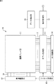
図1に示されるCMOSイメージセンサ10は、図示せぬ半導体基板上に形成された画素アレイ部11と、画素アレイ部11と同じ半導体基板上に集積された周辺回路部とを有する構成となっている。周辺回路部は、例えば、垂直駆動部12、カラム処理部13、水平駆動部14、およびシステム制御部15から構成されている。
A
さらに、CMOSイメージセンサ10は、信号処理部18およびデータ格納部19を備えている。
Further, the
画素アレイ部11は、受光した光量に応じた光電荷を生成し、蓄積する光電変換部を有する単位画素(以下、単に画素ともいう)が行方向および列方向に、すなわち、行列状に2次元配置された構成を採る。ここで、行方向とは画素行の画素の配列方向(水平方向)を表し、列方向とは画素列の画素の配列方向(垂直方向)を表している。画素アレイ部11には、複数の画素として、受光した被写体光に基づいて撮像画像を生成するための信号を生成する画素(撮像画素)と、焦点検出を行うための信号を生成する画素(位相差検出画素)とが配置される。
The
画素アレイ部11においては、行列状の画素配列に対して、画素行毎に画素駆動線16が行方向に沿って配線され、画素列毎に垂直信号線17が列方向に沿って配線されている。画素駆動線16は、画素から信号を読み出す際の駆動を行うための駆動信号を伝送する。図1では、画素駆動線16は1本の配線として示されているが、1本に限られるものではない。画素駆動線16の一端は、垂直駆動部12の各行に対応した出力端に接続されている。
In the
垂直駆動部12は、シフトレジスタやアドレスデコーダなどによって構成され、画素アレイ部11の各画素を全画素同時または行単位等で駆動する。すなわち、垂直駆動部12は、垂直駆動部12を制御するシステム制御部15とともに、画素アレイ部11の各画素を駆動する駆動部を構成している。垂直駆動部12は、その具体的な構成については図示を省略するが、一般的に、読出し走査系と掃出し走査系の2つの走査系を有する構成となっている。
The
読出し走査系は、単位画素から信号を読み出すために、画素アレイ部11の単位画素を行単位で順に選択走査する。単位画素から読み出される信号はアナログ信号である。掃出し走査系は、読出し走査系によって読出し走査が行われる読出し行に対して、その読出し走査よりもシャッタスピードの時間分だけ先行して掃出し走査を行う。
The readout scanning system selectively scans the unit pixels of the
この掃出し走査系による掃出し走査により、読出し行の単位画素の光電変換部から不要な電荷が掃出されることによって光電変換部がリセットされる。そして、この掃出し走査系による不要電荷の掃出す(リセットする)ことにより、電子シャッタ動作が行われる。ここで、電子シャッタ動作とは、光電変換部の光電荷を捨てて、新たに露光を開始する(光電荷の蓄積を開始する)動作のことをいう。 By the sweep scanning by the sweep scanning system, unnecessary charges are swept out from the photoelectric conversion unit of the unit pixel in the readout row, thereby resetting the photoelectric conversion unit. The electronic shutter operation is performed by sweeping (resetting) unnecessary charges by the sweep scanning system. Here, the electronic shutter operation refers to an operation in which the photoelectric charges in the photoelectric conversion unit are discarded and exposure is newly started (photocharge accumulation is started).
読出し走査系による読出し動作によって読み出される信号は、その直前の読出し動作または電子シャッタ動作以降に受光した光量に対応するものである。そして、直前の読出し動作による読出しタイミングまたは電子シャッタ動作による掃出しタイミングから、今回の読出し動作による読出しタイミングまでの期間が、単位画素における光電荷の露光期間となる。 The signal read by the reading operation by the reading scanning system corresponds to the amount of light received after the immediately preceding reading operation or electronic shutter operation. The period from the read timing by the immediately preceding read operation or the sweep timing by the electronic shutter operation to the read timing by the current read operation is the exposure period of the photo charge in the unit pixel.
垂直駆動部12によって選択走査された画素行の各単位画素から出力される信号は、画素列毎に垂直信号線17の各々を通してカラム処理部13に入力される。カラム処理部13は、画素アレイ部11の画素列毎に、選択行の各画素から垂直信号線17を通して出力される信号に対して所定の信号処理を行うとともに、信号処理後の画素信号を一時的に保持する。
A signal output from each unit pixel of the pixel row selectively scanned by the
具体的には、カラム処理部13は、信号処理として、少なくともノイズ除去処理、例えばCDS(Correlated Double Sampling)処理を行う。カラム処理部13によるCDS処理により、リセットノイズや画素内の増幅トランジスタの閾値ばらつき等の、画素固有の固定パターンノイズが除去される。カラム処理部13には、ノイズ除去処理以外に、例えば、AD(Analog-Digital)変換機能を持たせ、アナログの画素信号をデジタル信号に変換して出力させることも可能である。
Specifically, the
水平駆動部14は、シフトレジスタやアドレスデコーダなどによって構成され、カラム処理部13の画素列に対応する単位回路を順番に選択する。水平駆動部14による選択走査により、カラム処理部13において単位回路毎に信号処理された画素信号が順番に出力される。
The horizontal drive unit 14 includes a shift register, an address decoder, and the like, and sequentially selects unit circuits corresponding to the pixel columns of the
システム制御部15は、各種のタイミング信号を生成するタイミングジェネレータ等によって構成され、そのタイミングジェネレータで生成された各種のタイミング信号を基に、垂直駆動部12、カラム処理部13、および水平駆動部14等の駆動制御を行う。
The
信号処理部18は、少なくとも演算処理機能を有し、カラム処理部13から出力される画素信号に対して演算処理等の種々の信号処理を行う。データ格納部19は、信号処理部18での信号処理に必要なデータを一時的に格納する。
The
なお、信号処理部18およびデータ格納部19は、CMOSイメージセンサ10と同じ基板(半導体基板)上に搭載されても構わないし、CMOSイメージセンサ10とは別の基板上に配置されるようにしても構わない。また、信号処理部18およびデータ格納部19の各処理は、CMOSイメージセンサ10とは別の基板に設けられる外部信号処理部、例えば、DSP(Digital Signal Processor)回路やソフトウエアによる処理として実行されても構わない。
The
また、CMOSイメージセンサ10が裏面照射型のCMOSイメージセンサである場合、画素アレイ部11を含む半導体基板とロジック回路を含む半導体基板とを貼り合わせた、積層型のCMOSイメージセンサとして構成されるようにしてもよい。
When the
<画素アレイ部の画素配列>
次に、図2を参照して、画素アレイ部11の画素配置について説明する。
<Pixel array of pixel array section>
Next, the pixel arrangement of the
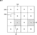
図2に示されるように、画素アレイ部11には、黒色の正方形で示される複数の撮像画素31が行列状に2次元配置されている。撮像画素31は、R画素、G画素、およびB画素からなり、これらは、ベイヤ配列に従い規則的に配置されている。
As shown in FIG. 2, in the
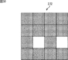
また、画素アレイ部11には、行列状に2次元配置される複数の撮像画素31の中に、白色の正方形で示される複数の位相差検出画素32が散在して配置されている。具体的には、位相差検出画素32は、画素アレイ部11における画素行のうちの所定の1行において、撮像画素31の一部を置き換えることで、特定のパターンで規則的に配置されている。なお、画素アレイ部11における撮像画素31および位相差検出画素32の配置は、これに限られるものではなく、他のパターンで配置されるようにしてもよい。
Further, in the
以下、画素アレイ部11における撮像画素31および位相差検出画素32の実施の形態について説明する。
Hereinafter, embodiments of the
<第1の実施の形態の画素の構成例>
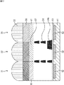
図3は、CMOSイメージセンサ10における第1の実施の形態の画素の構成例を示す断面図である。図3においては、CMOSイメージセンサ10における撮像画素31および位相差検出画素32の断面図が示されている。
<Configuration Example of Pixel of First Embodiment>
FIG. 3 is a cross-sectional view showing a configuration example of the pixel of the first embodiment in the
図3に示されるように、撮像画素31においては、半導体基板51に、入射した光を受光し光電変換を行う光電変換部52が形成され、半導体基板51の上層には、SiO等からなる絶縁層53が形成されている。絶縁層53の上には、CuやAlからなる複数の配線層54が形成されている。
As shown in FIG. 3, in the
配線層54の上には、感光性を有する高屈折率材料からなる高屈折率膜55が形成されている。感光性を有する高屈折率材料としては、例えば、TiO2,ZrO2,ZnO等が挙げられる。高屈折率膜55の屈折率は、1.5乃至2.0の間の値とされる。屈折率膜55の上には、撮像画素31それぞれに応じた分光特性を有するカラーフィルタ層56が形成され、カラーフィルタ層56の上には、マイクロレンズ57が形成されている。
On the
一方、位相差検出画素32においても、撮像画素31と同様に、半導体基板51、光電変換部52、絶縁層53、配線層54、カラーフィルタ層56、およびマイクロレンズ57が形成されている。
On the other hand, in the phase
さらに、位相差検出画素32においては、配線層54の一部が、光電変換部52に入射する光の一部を遮光する遮光膜54aとして、光電変換部52の受光領域の略半分の大きさの開口を有するように形成されている。また、配線層54とカラーフィルタ層56との間には、感光性を有しない低屈折率材料からなる低屈折率膜58が形成されている。感光性を有しない低屈折率材料としては、例えば、中空シリカ等が挙げられる。この低屈折率膜58は、撮像画素31における高屈折率膜55を覆うように形成され、カラーフィルタ層56が形成される際の平坦化膜を兼ねている。低屈折率膜58の屈折率は、1.1乃至1.5の間の値とされる。
Further, in the phase
なお、位相差検出画素32においては、カラーフィルタ層56に代えて、カラーフィルタ層56と同程度に入射光量を低減させるための減光フィルタが形成されるようにしてもよい。
In the phase
また、撮像画素31および位相差検出画素32において、マイクロレンズ57は一様に、すなわち、同一の形状、大きさで形成されており、同一の集光ポイントをもつものとするが、高屈折率膜55や低屈折率膜58の屈折率や膜厚が調整されることによって細かく設定されるようにすることができる。
Further, in the
すなわち、撮像画素31において、マイクロレンズ57の集光ポイントは、高屈折率膜55によって、光電変換部52の受光面に設定され、位相差検出画素32において、マイクロレンズ57の集光ポイントは、低屈折率膜58によって、遮光膜54aの上面に設定されるようにすることができる。
That is, in the
本実施の形態の構成によれば、撮像画素31において、光電変換部52より上に高屈折率膜55を設け、位相差検出画素32において、光電変換部52より上に低屈折率膜58を設けるようにしたので、撮像画素31においては、マイクロレンズ57の集光ポイントを光電変換部52の受光面としつつ、位相差検出画素32においては、マイクロレンズ57の集光ポイントを遮光膜54aの上面とすることができる。すなわち、撮像画素の感度と位相差検出画素のAF性能とを最適にすることが可能となる。
According to the configuration of the present embodiment, the
また、撮像画素31および位相差検出画素32においては、マイクロレンズ57が一様に形成されるので、マイクロレンズの形成プロセスを容易にすることができる。
Further, since the
<画素形成の流れについて>
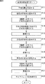
次に、図4乃至図6を参照して、本実施の形態の画素形成の流れについて説明する。図4は、画素形成処理について説明するフローチャートであり、図5および図6は、画素形成の工程を示す断面図である。
<Flow of pixel formation>
Next, the flow of pixel formation according to the present embodiment will be described with reference to FIGS. FIG. 4 is a flowchart for explaining the pixel formation process, and FIGS. 5 and 6 are cross-sectional views showing the pixel formation process.
以下においては、図5Aに示されるように、配線層54が形成された後の処理について説明する。
Hereinafter, as shown in FIG. 5A, a process after the
ステップS11において、図5Bに示されるように、配線層54の上に、感光性を有する高屈折率材料55aが塗布される。高屈折率材料55aの膜厚は、例えば400nmとされるが、マイクロレンズ57の集光ポイントに応じて調整される。また、高屈折率材料55aの屈折率は、例えば1.8とされるが、後述する低屈折率材料の屈折率と比べて0.1以上高ければよい。
In step S <b> 11, as shown in FIG. 5B, a photosensitive high
高屈折率材料55aが塗布された後、高屈折率材料55aの溶剤の除去および高屈折率材料55aの硬化のために、90℃での加熱が2分間行われる。
After the high
ステップS12において、フォトリソグラフィにより、撮像画素31の領域の高屈折率材料55aがパターン形成される。高屈折率材料55aは、例えば、画素サイズと略同じサイズ(画素サイズの±15%以内の範囲のサイズ)でパターン形成される。これにより、図5Cに示されるように、高屈折率膜55が形成されるようになる。
In step S12, the high
高屈折率膜55が形成された後、高屈折率膜55の硬化のために、200℃での加熱が5分間行われる。
After the high
ステップS13において、図6Dに示されるように、感光性を有しない低屈折率材料58aが、スピンコートにより、高屈折率膜55を覆うように塗布される。低屈折率材料58aの膜厚は、例えば600nmとされるが、マイクロレンズ57の集光ポイントに応じて調整される。また、低屈折率材料58aの屈折率は、例えば1.2とされるが、上述した高屈折率材料55aの屈折率と比べて0.1以上低ければよい。
In step S13, as shown in FIG. 6D, a low
これにより、位相差検出画素32の領域に、低屈折率膜58が形成されるようになる。なお、低屈折率材料58aは、高屈折率膜55を覆うように塗布されるので、低屈折率材料58aが、後段の処理で形成されるカラーフィルタ層56に対する平坦化膜として機能するようになる。
As a result, the low
低屈折率材料58aが塗布された後、低屈折率材料58aの溶剤の除去および低屈折率材料58aの硬化のために、230℃での加熱が5分間行われる。
After the low
ステップS14において、図6Eに示されるように、カラーフィルタ層56が、画素毎に形成される。
In step S14, as shown in FIG. 6E, the
そして、ステップS15において、図6Fに示されるように、マイクロレンズ57が、撮像画素31か位相差検出画素32かによらず一様に形成される。マイクロレンズ57は、マイクロレンズ材料が、スピンコートにより成膜され、フォトリソグラフィ工程を経て、マイクロレンズ材料がエッチバックされることで形成される。
In step S15, as shown in FIG. 6F, the
このようにして、撮像画素31と位相差検出画素32とが形成される。
In this way, the
以上の処理によれば、撮像画素31において、光電変換部52より上に高屈折率膜55が形成され、位相差検出画素32において、光電変換部52より上に低屈折率膜58が形成されるので、撮像画素31においては、マイクロレンズ57の集光ポイントを光電変換部52の受光面としつつ、位相差検出画素32においては、マイクロレンズ57の集光ポイントを遮光膜54aの上面とすることができる。すなわち、撮像画素の感度と位相差検出画素のAF性能とを最適にすることが可能となる。
According to the above process, the high
また、上述した処理においては、マイクロレンズは一様に形成されるので、集光特性のばらつきによる画像の劣化を抑えることが可能となる。 In the above-described processing, since the microlenses are formed uniformly, it is possible to suppress image degradation due to variations in light collection characteristics.
<画素の他の構成例>
なお、以上においては、撮像画素31における高屈折率膜55の断面形状は矩形であるものとしたが、フォトリソグラフィにより、図7に示されるように、高屈折率膜55の断面形状が、上凸型のレンズ形状に形成されるようにしてもよい。
<Other pixel configuration examples>
In the above description, the cross-sectional shape of the high-
<第2の実施の形態の画素の構成例>
次に、図8を参照して、第2の実施の形態の画素の構成例について説明する。
<Configuration Example of Pixel of Second Embodiment>
Next, a configuration example of the pixel according to the second embodiment will be described with reference to FIG.
なお、図8に示される撮像画素31および位相差検出画素32と、図3に示される撮像画素31および位相差検出画素32とで、同様にして形成される部分については、その説明を省略する。
The description of the portions formed in the same manner in the
図8に示されるように、撮像画素31において、配線層54とカラーフィルタ層56との間には、感光性を有しない高屈折率材料からなる高屈折率膜71が形成されている。感光性を有しない高屈折率材料としては、例えば、TiO2,ZrO2,ZnO等が挙げられる。この高屈折率膜71は、位相差検出画素32における低屈折率膜72を覆うように形成され、カラーフィルタ層56が形成される際の平坦化膜を兼ねている。
As shown in FIG. 8, in the
また、位相差検出画素32において、配線層54とカラーフィルタ層56との間には、感光性を有する低屈折率材料からなる低屈折率膜72が形成されている。感光性を有する低屈折率材料としては、例えば、中空シリカ等が挙げられる。図8においては、低屈折率膜72は、断面形状が上凸型のレンズ形状となるように形成されているが、矩形形状となるように形成されるようにしてもよい。
In the phase
本実施の形態においても、撮像画素31および位相差検出画素32において、マイクロレンズ57は一様に、すなわち、同一の形状、大きさで形成されており、同一の集光ポイントをもつものとするが、高屈折率膜71や低屈折率膜72の屈折率や膜厚が調整されることによって細かく設定されるようにすることができる。
Also in the present embodiment, in the
すなわち、撮像画素31において、マイクロレンズ57の集光ポイントは、高屈折率膜71によって、光電変換部52の受光面に設定され、位相差検出画素32において、マイクロレンズ57の集光ポイントは、低屈折率膜72によって、遮光膜54aの上面に設定されるようにすることができる。
That is, in the
本実施の形態の構成によれば、撮像画素31において、光電変換部52より上に高屈折率膜71を設け、位相差検出画素32において、光電変換部52より上に低屈折率膜72を設けるようにしたので、撮像画素31においては、マイクロレンズ57の集光ポイントを光電変換部52の受光面としつつ、位相差検出画素32においては、マイクロレンズ57の集光ポイントを遮光膜54aの上面とすることができる。すなわち、撮像画素の感度と位相差検出画素のAF性能とを最適にすることが可能となる。
According to the configuration of the present embodiment, the
<画素形成の流れについて>
次に、図9乃至図11を参照して、本実施の形態の画素形成の流れについて説明する。図9は、画素形成処理について説明するフローチャートであり、図10および図11は、画素形成の工程を示す断面図である。
<Flow of pixel formation>
Next, the flow of pixel formation according to the present embodiment will be described with reference to FIGS. FIG. 9 is a flowchart for explaining the pixel formation process, and FIGS. 10 and 11 are cross-sectional views showing the pixel formation process.
なお、以下においても、図10Aに示されるように、配線層54が形成された後の処理について説明する。
In the following, the process after the
ステップS31において、図10Bに示されるように、配線層54の上に、感光性を有する低屈折率材料72aが塗布される。低屈折率材料72aの膜厚は、例えば400nmとされるが、マイクロレンズ57の集光ポイントに応じて調整される。また、低屈折率材料72aの屈折率は、例えば1.4とされるが、後述する高屈折率材料の屈折率と比べて0.1以上低ければよい。
In step S31, as shown in FIG. 10B, a low
低屈折率材料72aが塗布された後、低屈折率材料72aの溶剤の除去および低屈折率材料72aの硬化のために、90℃での加熱が2分間行われる。
After the low
ステップS32において、フォトリソグラフィにより、図10Cに示されるように、位相差検出画素32の領域の低屈折率材料72aがパターン形成される。低屈折率材料72aは、例えば、画素サイズと略同じサイズ(画素サイズの±15%以内の範囲のサイズ)でパターン形成される。
In step S32, the low
ステップS33において、加熱が行われ、低屈折率材料72aがリフローされることで、低屈折率材料72aがレンズ形状に形成される。ここでは、例えば、140℃での加熱が2分間、175℃での加熱が2分間と、段階的に加熱が行われるようにする。これにより、図10Dに示されるように、断面形状が上凸型レンズ形状の低屈折率膜72が形成されるようになる。
In step S33, heating is performed and the low
レンズ形状が形成された後、低屈折率材料72aに含まれる感光材の分解と低屈折率材料72aの硬化のために、UV(Ultra Violet)光を照射させながら、250℃での加熱が行われる。
After the lens shape is formed, heating at 250 ° C. is performed while irradiating UV (Ultra Violet) light to decompose the photosensitive material contained in the low
ステップS34において、図11Eに示されるように、感光性を有しない高屈折率材料71aが、スピンコートにより、低屈折率膜72を覆うように塗布される。高屈折率材料71aの膜厚は、例えば600nmとされるが、マイクロレンズ57の集光ポイントに応じて調整される。また、高屈折率材料71aの屈折率は、例えば1.8とされるが、上述した低屈折率材料72aの屈折率と比べて0.1以上高ければよい。
In step S34, as shown in FIG. 11E, a high
これにより、撮像画素31の領域に、高屈折率膜71が形成されるようになる。なお、高屈折率材料71aは、低屈折率膜72を覆うように塗布されるので、高屈折率材料71aが、後段の処理で形成されるカラーフィルタ層56に対する平坦化膜として機能するようになる。
Thereby, the high
高屈折率材料71aが塗布された後、高屈折率材料71aの溶剤の除去および高屈折率材料71aの硬化のために、230℃での加熱が5分間行われる。
After the high
ステップS35において、図11Fに示されるように、カラーフィルタ層56が、画素毎に形成される。
In step S35, as shown in FIG. 11F, the
そして、ステップS36において、図11Gに示されるように、マイクロレンズ57が、第1の実施の形態と同様に、撮像画素31か位相差検出画素32かによらず一様に形成される。
In step S36, as shown in FIG. 11G, the
このようにして、撮像画素31と位相差検出画素32とが形成される。
In this way, the
以上の処理によれば、撮像画素31において、光電変換部52より上に高屈折率膜71が形成され、位相差検出画素32において、光電変換部52より上に低屈折率膜72が形成されるので、撮像画素31においては、マイクロレンズ57の集光ポイントを光電変換部52の受光面としつつ、位相差検出画素32においては、マイクロレンズ57の集光ポイントを遮光膜54aの上面とすることができる。すなわち、撮像画素の感度と位相差検出画素のAF性能とを最適にすることが可能となる。
According to the above processing, the high
また、上述した処理においても、マイクロレンズは一様に形成されるので、集光特性のばらつきによる画像の劣化を抑えることが可能となる。 Also, in the above-described processing, since the microlenses are formed uniformly, it is possible to suppress image degradation due to variations in light collection characteristics.
<第3の実施の形態の画素の構成例>
次に、図12を参照して、第3の実施の形態の画素の構成例について説明する。
<Configuration Example of Pixel of Third Embodiment>
Next, a configuration example of the pixel according to the third embodiment will be described with reference to FIG.
なお、図12に示される撮像画素31および位相差検出画素32と、図3に示される撮像画素31および位相差検出画素32とで、同様にして形成される部分については、その説明を省略する。
It should be noted that description of portions formed in the same manner in the
図12に示されるように、撮像画素31において、配線層54とカラーフィルタ層56との間には、感光性を有する高屈折率材料からなる高屈折率膜81が形成されている。感光性を有する高屈折率材料としては、例えば、TiO2,ZrO2,ZnO等が挙げられる。
As shown in FIG. 12, in the
また、位相差検出画素32において、配線層54とカラーフィルタ層56との間には、感光性を有する低屈折率材料からなる低屈折率膜82が形成されている。感光性を有する低屈折率材料としては、例えば、中空シリカ等が挙げられる。
In the phase
本実施の形態においても、撮像画素31および位相差検出画素32において、マイクロレンズ57は一様に、すなわち、同一の形状、大きさで形成されており、同一の集光ポイントをもつものとするが、高屈折率膜81や低屈折率膜82の屈折率や膜厚が調整されることによって細かく設定されるようにすることができる。
Also in the present embodiment, in the
すなわち、撮像画素31において、マイクロレンズ57の集光ポイントは、高屈折率膜81によって、光電変換部52の受光面に設定され、位相差検出画素32において、マイクロレンズ57の集光ポイントは、低屈折率膜82によって、遮光膜54aの上面に設定されるようにすることができる。
That is, in the
本実施の形態の構成によれば、撮像画素31において、光電変換部52より上に高屈折率膜81を設け、位相差検出画素32において、光電変換部52より上に低屈折率膜82を設けるようにしたので、撮像画素31においては、マイクロレンズ57の集光ポイントを光電変換部52の受光面としつつ、位相差検出画素32においては、マイクロレンズ57の集光ポイントを遮光膜54aの上面とすることができる。すなわち、撮像画素の感度と位相差検出画素のAF性能とを最適にすることが可能となる。
According to the configuration of the present embodiment, the
<画素形成の流れについて>
次に、図13乃至図15を参照して、本実施の形態の画素形成の流れについて説明する。図13は、画素形成処理について説明するフローチャートであり、図14および図15は、画素形成の工程を示す断面図である。
<Flow of pixel formation>
Next, the flow of pixel formation according to the present embodiment will be described with reference to FIGS. FIG. 13 is a flowchart for explaining the pixel formation process, and FIGS. 14 and 15 are cross-sectional views showing the pixel formation process.
なお、以下においても、図14Aに示されるように、配線層54が形成された後の処理について説明する。
In the following, the process after the
ステップS51において、図14Bに示されるように、配線層54の上に、感光性を有する低屈折率材料82aが、スピンコートにより塗布される。低屈折率材料82aの膜厚は、例えば400nmとされるが、マイクロレンズ57の集光ポイントに応じて調整される。また、低屈折率材料82aの屈折率は、例えば1.4とされるが、後述する高屈折率材料の屈折率と比べて0.1以上低ければよい。なお、低屈折率材料82aは、ネガ型のレジストであってもよいし、ポジ型のレジストであってもよい。
In step S51, as shown in FIG. 14B, a photosensitive low
ステップS52において、フォトリソグラフィにより露光、現像することで、位相差検出画素32の領域の低屈折率材料82aがパターン形成される。これにより、図14Cに示されるように、低屈折率膜82が形成されるようになる。
In step S52, the low
ここでは、現像後、低屈折率材料82aの溶剤の除去および低屈折率材料82aの硬化のために、200℃での加熱が10分間行われる。
Here, after development, heating at 200 ° C. is performed for 10 minutes in order to remove the solvent of the low
ステップS53において、図14Dに示されるように、感光性を有する高屈折率材料81aが、スピンコートにより、低屈折率膜82を覆うように塗布される。高屈折率材料81aの膜厚は、例えば400nmとされるが、マイクロレンズ57の集光ポイントに応じて調整される。また、高屈折率材料81aの屈折率は、例えば1.8とされるが、上述した低屈折率材料82aの屈折率と比べて0.1以上高ければよい。なお、高屈折率材料81aは、ネガ型のレジストであってもよいし、ポジ型のレジストであってもよい。
In step S53, as shown in FIG. 14D, a photosensitive high
ステップS54において、フォトリソグラフィにより露光、現像することで、撮像画素31の領域の高屈折率材料81aがパターン形成される。これにより、図15Eに示されるように、高屈折率膜81が形成されるようになる。
In step S54, the high
ここでは、現像後、高屈折率材料81aの溶剤の除去および高屈折率材料81aの硬化のために、200℃での加熱が10分間行われる。
Here, after the development, heating at 200 ° C. is performed for 10 minutes in order to remove the solvent of the high
ステップS55において、図15Fに示されるように、カラーフィルタ層56が、画素毎に形成される。
In step S55, as shown in FIG. 15F, the
そして、ステップS56において、図15Gに示されるように、マイクロレンズ57が、第1の実施の形態と同様に、撮像画素31か位相差検出画素32かによらず一様に形成される。
In step S56, as shown in FIG. 15G, the
このようにして、撮像画素31と位相差検出画素32とが形成される。
In this way, the
以上の処理によれば、撮像画素31において、光電変換部52より上に高屈折率膜81が形成され、位相差検出画素32において、光電変換部52より上に低屈折率膜82が形成されるので、撮像画素31においては、マイクロレンズ57の集光ポイントを光電変換部52の受光面としつつ、位相差検出画素32においては、マイクロレンズ57の集光ポイントを遮光膜54aの上面とすることができる。すなわち、撮像画素の感度と位相差検出画素のAF性能とを最適にすることが可能となる。
According to the above process, the high
また、上述した処理においても、マイクロレンズは一様に形成されるので、集光特性のばらつきによる画像の劣化を抑えることが可能となる。 Also, in the above-described processing, since the microlenses are formed uniformly, it is possible to suppress image degradation due to variations in light collection characteristics.
なお、上述した処理においては、低屈折率膜82が形成された後に、高屈折率膜81が形成されるようにしたが、高屈折率膜81が形成された後に、低屈折率膜82が形成されるようにしてもよい。
In the above-described processing, the high
<画素形成の流れの他の例>
ここで、図16乃至図18を参照して、本実施の形態の画素形成の流れについて説明する。図16は、画素形成処理について説明するフローチャートであり、図17および図18は、画素形成の工程を示す断面図である。
<Another example of pixel formation flow>
Here, with reference to FIG. 16 to FIG. 18, a flow of pixel formation of the present embodiment will be described. FIG. 16 is a flowchart for explaining the pixel formation process, and FIGS. 17 and 18 are cross-sectional views showing the pixel formation process.
なお、以下においても、図17Aに示されるように、配線層54が形成された後の処理について説明する。
In the following, the process after the
ステップS71において、図17Bに示されるように、配線層54の上に、感光性を有する高屈折率材料81aが、スピンコートにより塗布される。高屈折率材料81aの膜厚は、例えば500nmとされるが、マイクロレンズ57の集光ポイントに応じて調整される。また、高屈折率材料81aの屈折率は、例えば1.8とされるが、後述する低屈折率材料の屈折率と比べて0.1以上高ければよい。なお、高屈折率材料81aは、ネガ型のレジストであってもよいし、ポジ型のレジストであってもよい。
In step S71, as shown in FIG. 17B, a photosensitive high
ステップS72において、フォトリソグラフィにより露光、現像することで、撮像画素31の領域の高屈折率材料81aがパターン形成される。これにより、図17Cに示されるように、高屈折率膜81が形成されるようになる。
In step S72, the high
ここでは、現像後、高屈折率材料81aの溶剤の除去および高屈折率材料81aの硬化のために、200℃での加熱が10分間行われる。
Here, after the development, heating at 200 ° C. is performed for 10 minutes in order to remove the solvent of the high
ステップS73において、図17Dに示されるように、感光性を有する低屈折率材料82aが、スピンコートにより、高屈折率膜81を覆うように塗布される。低屈折率材料82aの膜厚は、例えば400nmとされるが、マイクロレンズ57の集光ポイントに応じて調整される。また、低屈折率材料82aの屈折率は、例えば1.2とされるが、上述した高屈折率材料81aの屈折率と比べて0.1以上低ければよい。なお、低屈折率材料82aは、ネガ型のレジストであってもよいし、ポジ型のレジストであってもよい。
In step S73, as shown in FIG. 17D, a low
ステップS74において、フォトリソグラフィにより露光、現像することで、位相差検出画素32の領域の低屈折率材料82aがパターン形成される。これにより、図18Eに示されるように、低屈折率膜82が形成されるようになる。
In step S74, the low
ここでは、現像後、低屈折率材料82aの溶剤の除去および低屈折率材料82aの硬化のために、200℃での加熱が10分間行われる。
Here, after development, heating at 200 ° C. is performed for 10 minutes in order to remove the solvent of the low
ステップS75において、図17Fに示されるように、カラーフィルタ層56が、画素毎に形成される。
In step S75, as shown in FIG. 17F, the
そして、ステップS76において、図17Gに示されるように、マイクロレンズ57が、第1の実施の形態と同様に、撮像画素31か位相差検出画素32かによらず一様に形成される。
In step S76, as shown in FIG. 17G, the
このようにしても、撮像画素31と位相差検出画素32とが形成される。
Even in this way, the
<第4の実施の形態の画素の構成例>
次に、図19を参照して、第4の実施の形態の画素の構成例について説明する。
<Example of Configuration of Pixel of Fourth Embodiment>
Next, a configuration example of the pixel according to the fourth embodiment will be described with reference to FIG.
なお、図19に示される撮像画素31および位相差検出画素32と、図3に示される撮像画素31および位相差検出画素32とで、同様にして形成される部分については、その説明を省略する。
In addition, the description is abbreviate | omitted about the part formed similarly in the
図19に示されるように、撮像画素31において、配線層54とカラーフィルタ層56との間には、感光性を有しない高屈折率材料からなる高屈折率膜91が形成されている。感光性を有しない高屈折率材料としては、例えば、TiO2,ZrO2,ZnO等が挙げられる。
As shown in FIG. 19, in the
また、位相差検出画素32において、配線層54とカラーフィルタ層56との間には、感光性を有する低屈折率材料からなる低屈折率膜92が形成されている。感光性を有する低屈折率材料としては、例えば、中空シリカ等が挙げられる。
In the phase
本実施の形態においても、撮像画素31および位相差検出画素32において、マイクロレンズ57は一様に、すなわち、同一の形状、大きさで形成されており、同一の集光ポイントをもつものとするが、高屈折率膜91や低屈折率膜92の屈折率や膜厚が調整されることによって細かく設定されるようにすることができる。
Also in the present embodiment, in the
すなわち、撮像画素31において、マイクロレンズ57の集光ポイントは、高屈折率膜91によって、光電変換部52の受光面に設定され、位相差検出画素32において、マイクロレンズ57の集光ポイントは、低屈折率膜92によって、遮光膜54aの上面に設定されるようにすることができる。
That is, in the
本実施の形態の構成によれば、撮像画素31において、光電変換部52より上に高屈折率膜91を設け、位相差検出画素32において、光電変換部52より上に低屈折率膜92を設けるようにしたので、撮像画素31においては、マイクロレンズ57の集光ポイントを光電変換部52の受光面としつつ、位相差検出画素32においては、マイクロレンズ57の集光ポイントを遮光膜54aの上面とすることができる。すなわち、撮像画素の感度と位相差検出画素のAF性能とを最適にすることが可能となる。
According to the configuration of the present embodiment, the
<画素形成の流れについて>
次に、図20乃至図22を参照して、本実施の形態の画素形成の流れについて説明する。図20は、画素形成処理について説明するフローチャートであり、図21および図22は、画素形成の工程を示す断面図である。
<Flow of pixel formation>
Next, the flow of pixel formation according to the present embodiment will be described with reference to FIGS. FIG. 20 is a flowchart for explaining the pixel formation process, and FIGS. 21 and 22 are cross-sectional views showing the pixel formation process.
なお、以下においても、図21Aに示されるように、配線層54が形成された後の処理について説明する。
In the following, as shown in FIG. 21A, the processing after the
ステップS91において、図21Bに示されるように、配線層54の上に、感光性を有しない高屈折率材料91aが、スピンコートにより塗布される。高屈折率材料91aの膜厚は、例えば500nmとされるが、マイクロレンズ57の集光ポイントに応じて調整される。また、高屈折率材料91aの屈折率は、例えば1.8とされるが、後述する低屈折率材料の屈折率と比べて0.1以上高ければよい。
In step S91, as shown in FIG. 21B, a high
高屈折率材料91aが塗布された後、高屈折率材料91aの溶剤の除去および高屈折率材料91aの硬化のために、200℃での加熱が10分間行われる。
After the high
ステップS92において、図21Cに示されるように、高屈折率材料91a上の位相差検出画素32以外の領域(すなわち、撮像画素31の領域)に、フォトレジスト101が形成される。
In step S92, as shown in FIG. 21C, the
ステップS93において、位相差検出画素32の領域の高屈折率材料91aが、ドライエッチングされる。これにより、図21Dに示されるように、高屈折率膜91が形成されるようになる。
In step S93, the high
ステップS94において、図22Eに示されるように、感光性を有する低屈折率材料92aが、スピンコートにより、高屈折率膜91を覆うように塗布される。低屈折率材料92aの膜厚は、例えば400nmとされるが、マイクロレンズ57の集光ポイントに応じて調整される。また、低屈折率材料92aの屈折率は、例えば1.4とされるが、上述した高屈折率材料91aの屈折率と比べて0.1以上低ければよい。なお、低屈折率材料92aは、ネガ型のレジストであってもよいし、ポジ型のレジストであってもよい。
In step S94, as shown in FIG. 22E, a low
ステップS95において、フォトリソグラフィにより露光、現像することで、位相差検出画素32の領域の低屈折率材料92aがパターン形成される。これにより、図22Fに示されるように、低屈折率膜92が形成されるようになる。
In step S95, the low
ここでは、位相差検出画素32の領域のみに、露光量5000J/m2、フォーカスオフセット0μmでi線露光が行われ、現像後、低屈折率材料92aの溶剤の除去および低屈折率材料82aの硬化のために、200℃での加熱が10分間行われるようにする。
Here, only the region of the phase
ステップS96において、図22Gに示されるように、カラーフィルタ層56が、画素毎に形成される。
In step S96, as shown in FIG. 22G, the
そして、ステップS97において、図22Hに示されるように、マイクロレンズ57が、第1の実施の形態と同様に、撮像画素31か位相差検出画素32かによらず一様に形成される。
In step S97, as shown in FIG. 22H, the
以上の処理によれば、撮像画素31において、光電変換部52より上に高屈折率膜91が形成され、位相差検出画素32において、光電変換部52より上に低屈折率膜92が形成されるので、撮像画素31においては、マイクロレンズ57の集光ポイントを光電変換部52の受光面としつつ、位相差検出画素32においては、マイクロレンズ57の集光ポイントを遮光膜54aの上面とすることができる。すなわち、撮像画素の感度と位相差検出画素のAF性能とを最適にすることが可能となる。
According to the above process, the high
以上においては、本技術を表面照射型のCMOSイメージセンサに適用した構成について説明してきたが、以下においては、本技術を裏面照射型のCMOSイメージセンサに適用した構成について説明する。 The configuration in which the present technology is applied to a front-illuminated CMOS image sensor has been described above, but the configuration in which the present technology is applied to a back-illuminated CMOS image sensor will be described below.
<第5の実施の形態の画素の構成例>
図23は、裏面照射型のCMOSイメージセンサ10における第5の実施の形態の画素の構成例を示す断面図である。図23においては、裏面照射型のCMOSイメージセンサ10における撮像画素31および位相差検出画素32の断面図が示されている。
<Configuration Example of Pixel of Fifth Embodiment>
FIG. 23 is a cross-sectional view illustrating a configuration example of a pixel according to the fifth embodiment of the backside illumination type
図23に示されるように、撮像画素31においては、半導体基板151に光電変換部152が形成され、半導体基板151の上層には、絶縁層153が形成されている。
As shown in FIG. 23, in the
絶縁層153の上には、高屈折率材料からなる高屈折率膜154が形成されている。高屈折率膜154は、感光性を有する高屈折率材料からなるようにしてもよいし、感光性を有しない高屈折率材料からなるようにしてもよい。高屈折率膜154の上には、カラーフィルタ層155が形成され、カラーフィルタ層155の上には、マイクロレンズ156が形成されている。
A high
一方、位相差検出画素32においても、撮像画素31と同様に、半導体基板151、光電変換部152、絶縁層153、カラーフィルタ層155、およびマイクロレンズ156が形成されている。
On the other hand, in the phase
さらに、位相差検出画素32においては、絶縁層153上に、遮光膜157が、光電変換部152の受光領域の略半分の大きさの開口を有するように形成されている。そして、カラーフィルタ層155の下には、低屈折率材料からなる低屈折率膜158が形成されている。低屈折率膜158は、感光性を有する低屈折率材料からなるようにしてもよいし、感光性を有しない低屈折率材料からなるようにしてもよい。
Further, in the phase
なお、位相差検出画素32においては、カラーフィルタ層155に代えて、カラーフィルタ層155と同程度に入射光量を低減させるための減光フィルタが形成されるようにしてもよい。
In the phase
また、裏面照射型のCMOSイメージセンサ10においては、マイクロレンズ156が形成される面とは逆の面に、配線層159が形成される。
Further, in the backside illumination type
本実施の形態においても、撮像画素31および位相差検出画素32において、マイクロレンズ156は一様に、すなわち、同一の形状、大きさで形成されており、同一の集光ポイントをもつものとするが、高屈折率膜154や低屈折率膜158の屈折率や膜厚が調整されることによって細かく設定されるようにすることができる。
Also in the present embodiment, in the
すなわち、撮像画素31において、マイクロレンズ156の集光ポイントは、高屈折率膜154によって、光電変換部152の受光面に設定され、位相差検出画素32において、マイクロレンズ156の集光ポイントは、低屈折率膜158によって、遮光膜157の上面に設定されるようにすることができる。
That is, in the
本実施の形態の構成によれば、撮像画素31において、光電変換部152より上に高屈折率膜154を設け、位相差検出画素32において、光電変換部152より上に低屈折率膜158を設けるようにしたので、撮像画素31においては、マイクロレンズ156の集光ポイントを光電変換部152の受光面としつつ、位相差検出画素32においては、マイクロレンズ156の集光ポイントを遮光膜157の上面とすることができる。すなわち、撮像画素の感度と位相差検出画素のAF性能とを最適にすることが可能となる。
According to the configuration of the present embodiment, the
上述した構成においては、撮像画素において、光電変換部より上に高屈折率膜を設け、位相差検出画素において、光電変換部より上に低屈折率膜を設けることで、撮像画素の感度を最適にしつつ、位相差検出画素の感度を低下させないようにしたが、他の構成によりこれを実現することも可能である。 In the configuration described above, the sensitivity of the imaging pixel is optimized by providing a high refractive index film above the photoelectric conversion unit in the imaging pixel and providing a low refractive index film above the photoelectric conversion unit in the phase difference detection pixel. However, the sensitivity of the phase difference detection pixel is not lowered, but this can be realized by other configurations.
なお、以下においては、図24に示されるように、ベイヤ配列に従い規則的に配置されている撮像画素31としての、R画素31R、G画素31G、およびB画素31Bのうちの、G画素31Gの一部が、位相差検出画素32に置き換えられた構成について説明する。
In the following, as shown in FIG. 24, the
<第6の実施の形態の画素の構成例>
図25は、CMOSイメージセンサ10における第6の実施の形態の画素の構成例を示す断面図である。図25においては、CMOSイメージセンサ10における撮像画素31のうちのG画素31Gおよび位相差検出画素32の断面図が示されている。
<Configuration Example of Pixel of Sixth Embodiment>
FIG. 25 is a cross-sectional view illustrating a configuration example of the pixel of the sixth embodiment in the
図25に示されるように、撮像画素31においては、半導体基板251に、入射した光を受光し光電変換を行う光電変換部252が形成され、半導体基板251の上層には、SiO等からなる絶縁層253が形成されている。絶縁層253の上には、CuやAlからなる複数の配線層254が形成されている。
As shown in FIG. 25, in the
配線層254の上には、平坦化膜255が形成され、平坦化膜255の上には、G画素31Gに応じた分光特性を有する緑色のカラーフィルタ256Gが形成されている。カラーフィルタ256Gの上には、マイクロレンズ257が形成されている。なお、図25の例では、カラーフィルタ256Gと同じ層に、赤色のカラーフィルタ256Rが形成されているので、R画素31Rが、G画素31Gに隣接して形成されていることになる。
A
一方、位相差検出画素32においても、G画素31Gと同様に、半導体基板251、光電変換部252、絶縁層253、配線層254、およびマイクロレンズ257が形成されている。
On the other hand, also in the phase
さらに、位相差検出画素32においては、配線層254の一部が、光電変換部252に入射する光の一部を遮光する遮光膜254aとして、光電変換部252の受光領域の略半分の大きさの開口を有するように形成されている。また、カラーフィルタ256Gと同じ層には、カラーフィルタ256G'が形成されている。カラーフィルタ256G'は、その膜厚がカラーフィルタ256Gより薄くなるように形成されている。
Further, in the phase
従来、例えば、G画素の一部を位相差検出画素に置き換えた固体撮像装置においては、G画素(撮像画素)の感度を最適にするように、緑色のカラーフィルタの膜厚が決められていた。しかしながら、位相差検出画素においては、遮光膜により、その感度がG画素の感度より低くなってしまっていた。 Conventionally, for example, in a solid-state imaging device in which part of a G pixel is replaced with a phase difference detection pixel, the thickness of the green color filter is determined so as to optimize the sensitivity of the G pixel (imaging pixel). . However, the sensitivity of the phase difference detection pixel is lower than that of the G pixel due to the light shielding film.
本実施の形態の構成によれば、位相差検出画素32が有するカラーフィルタ256G'が、その膜厚が、G画素31Gが有するカラーフィルタ256Gの膜厚より薄くなるように形成されるようにしたので、撮像画素の感度を最適にしつつ、位相差検出画素の感度を低下させないようすることができる。すなわち、撮像画素の感度と位相差検出画素のAF性能とを最適にすることが可能となる。
According to the configuration of the present embodiment, the
なお、撮像画素31および位相差検出画素32において、マイクロレンズ257の形状や大きさは、カラーフィルタ256Gやカラーフィルタ256G'の膜厚に応じて決定されるようにしてもよい。
In the
<画素形成の流れについて>
次に、図26乃至図28を参照して、本実施の形態の画素形成の流れについて説明する。図26は、画素形成処理について説明するフローチャートであり、図27および図28は、画素形成の工程を示す断面図である。
<Flow of pixel formation>
Next, with reference to FIGS. 26 to 28, the flow of pixel formation in this embodiment will be described. FIG. 26 is a flowchart for explaining the pixel formation process, and FIGS. 27 and 28 are cross-sectional views showing the pixel formation process.
以下においては、配線層254が形成された後の処理について説明する。
Hereinafter, a process after the
ステップS111において、図27Aに示されるように、配線層254の上に、平坦化膜255が形成される。
In step S111, as shown in FIG. 27A, a
ステップS112において、図27Bに示されるように、平坦化膜255の上に、緑色のカラーフィルタ(CF)材料256gが塗布される。ここでは、CF材料256gとして、ネガ型のフォトレジストが用いられるものとする。なお、CF材料256gとして、ポジ型のフォトレジストが用いられるようにすることもできるが、この場合、露光に用いられるレチクルの露光パターンは、後述するレチクルの露光パターンを反転させたものとなり、露光条件も逆にする必要がある。
In step S112, as shown in FIG. 27B, a green color filter (CF)
ステップS113において、図27Cに示されるように、レチクル271を用いることで、G画素31Gに対応するCF材料256gが、所定の露光条件(露光量、露光照度等)で露光される。レチクル271は、図29に示されるように、G画素31Gが形成される画素領域のみを露光する露光パターン(図中白色の部分)を有している。これにより、図27Cに示されるように、CF材料256gにおける領域H1のみが露光されるようになる。
In step S113, as shown in FIG. 27C, by using the
続いてステップS114において、図27Dに示されるように、レチクル272を用いることで、位相差検出画素32に対応するCF材料256gが、ステップS113における露光条件とは異なる露光条件、具体的には、より少ない露光量、より低い露光照度等で露光される。レチクル272は、図30に示されるように、位相差検出画素32が形成される画素領域のみを露光する露光パターン(図中白色の部分)を有している。これにより、図27Dに示されるように、CF材料256gにおける領域H2のみが露光されるようになる。
Subsequently, in step S114, as shown in FIG. 27D, by using the
なお、ステップS113の処理とステップS114の処理は、中断されることなく連続して行われるものとする。 Note that the processing in step S113 and the processing in step S114 are performed continuously without interruption.
ステップS115において、CF材料256gが現像される。具体的には、CF材料256gにおいて、ステップS113またはステップS114で露光されなかった領域が現像液で除去される。このとき、CF材料256gにおいて、ステップS113またはステップS114で露光された領域のうち、領域H2の膜厚は、領域H1の膜厚と比較して薄くなる。
In step S115, the
このようにして、図28Eに示されるように、位相差検出画素32が有するカラーフィルタ256G'が、その膜厚が、G画素31Gが有するカラーフィルタ256Gの膜厚より薄くなるように形成される。
In this way, as shown in FIG. 28E, the
ステップS116において、平坦化膜255の上に、赤色のCF材料256r(図示せず)が塗布される。
In step S116, a red CF material 256r (not shown) is applied on the
ステップS117において、図示はしないが、R画素31Rが形成される画素領域のみを露光する露光パターンを有するレチクルを用いることで、R画素31Rに対応するCF材料256rが、所定の露光条件で露光される。
In step S117, although not shown, the CF material 256r corresponding to the
ステップS118において、CF材料256rが現像される。これにより、図28Fに示されるように、R画素31Rが有するカラーフィルタ256Rが形成される。なお、カラーフィルタ256Rの膜厚は、G画素31Gが有するカラーフィルタ256Gの膜厚と同一とされる。
In step S118, the CF material 256r is developed. As a result, as shown in FIG. 28F, a
ステップS119において、平坦化膜255の上に、青色のCF材料256b(図示せず)が塗布される。
In step S119, a blue CF material 256b (not shown) is applied on the
ステップS120において、図示はしないが、B画素31Bが形成される画素領域のみを露光する露光パターンを有するレチクルを用いることで、B画素31Bに対応するCF材料256bが、所定の露光条件で露光される。
In step S120, although not shown, the CF material 256b corresponding to the
ステップS121において、CF材料256bが現像される。これにより、B画素31Bが有するカラーフィルタ256B(図示せず)が形成される。なお、カラーフィルタ256Bの膜厚もまた、G画素31Gが有するカラーフィルタ256Gの膜厚と同一とされる。
In step S121, the CF material 256b is developed. As a result, a color filter 256B (not shown) included in the
以上のようにして、カラーフィルタが画素毎に形成された後、ステップS122において、図28Gに示されるように、マイクロレンズ257が、画素毎に形成される。マイクロレンズ257は、マイクロレンズ材料が、スピンコートにより成膜され、フォトリソグラフィ工程を経て、マイクロレンズ材料がエッチバックされることで形成される。
As described above, after the color filter is formed for each pixel, in step S122, as shown in FIG. 28G, the
このようにして、撮像画素31と位相差検出画素32とが形成される。
In this way, the
以上の処理によれば、位相差検出画素32が有するカラーフィルタ256G'が、その膜厚が、G画素31Gが有するカラーフィルタ256Gの膜厚より薄くなるように形成されるので、撮像画素の感度を最適にしつつ、位相差検出画素の感度を低下させないようすることができる。すなわち、撮像画素の感度と位相差検出画素のAF性能とを最適にすることが可能となる。
According to the above processing, the
また、ステップS113の処理とステップS114の処理が、中断されることなく連続して行われるようにしたので、CF材料の塗布、露光、現像の流れを1工程としてみた場合、R画素、G画素、およびB画素がベイヤ配列で配置される一般的な画素の形成処理と同じ3工程で、撮像画素31と位相差検出画素32とを形成することができ、工程数の増加を避けることが可能となる。
In addition, since the process of step S113 and the process of step S114 are continuously performed without interruption, when the flow of CF material application, exposure, and development is considered as one process, R pixel and G pixel In addition, the
なお、上述した処理においては、G画素31Gが形成される画素領域の露光と、位相差検出画素32が形成される画素領域の露光とが別個に行われるようにしたが、一括して行われるようにしてもよい。
In the above-described processing, the exposure of the pixel region in which the
<画素形成の流れの他の例>
そこで、図31および図32を参照して、本実施の形態の画素形成の流れの他の例について説明する。図31は、画素形成処理について説明するフローチャートであり、図32は、画素形成の工程を示す断面図である。
<Another example of pixel formation flow>
Therefore, another example of the pixel formation flow of the present embodiment will be described with reference to FIGS. FIG. 31 is a flowchart for explaining pixel formation processing, and FIG. 32 is a cross-sectional view showing a pixel formation process.
なお、以下においても、配線層254が形成された後の処理について説明する。
In the following, the processing after the
ステップS131において、図32Aに示されるように、配線層254の上に、平坦化膜255が形成される。
In step S131, as shown in FIG. 32A, a
ステップS132において、図32Bに示されるように、平坦化膜255の上に、緑色のCF材料256gが塗布される。
In step S132, as shown in FIG. 32B, a
ステップS133において、図32Cに示されるように、グレースケールマスク281を用いることで、G画素31Gおよび位相差検出画素32に対応するCF材料256gが、所定の露光条件(露光量、露光照度等)で露光される。グレースケールマスク281は、図33に示されるように、G画素31Gが形成される画素領域を露光する第1の露光パターン(図中白色の部分)と、位相差検出画素32が形成される画素領域を露光する第2の露光パターン(図中薄い灰色の部分)とを有している。グレースケールマスク281において、第2の露光パターンの光透過率は、第1の露光パターンの光透過率と異なる(具体的には、第1の露光パターンの光透過率より低くなる)ようになされている。これにより、図32Cに示されるように、CF材料256gにおける領域H2は、領域H1より少ない露光量、少ない露光照度で露光されるようになる。
In step S133, as shown in FIG. 32C, the
ステップS134において、CF材料256gが現像される。具体的には、CF材料256gにおいて、ステップS133で露光されなかった領域が現像液で除去される。このとき、CF材料256gにおいて、ステップS133で露光された領域のうち、領域H2の膜厚は、領域H1の膜厚と比較して薄くなる。
In step S134, the
このようにして、図32Dに示されるように、位相差検出画素32が有するカラーフィルタ256G'が、その膜厚が、G画素31Gが有するカラーフィルタ256Gの膜厚より薄くなるように形成される。
In this way, as shown in FIG. 32D, the
なお、ステップS135以降の処理については、図26のフローチャートのステップS116以降の処理と同様であるので、その説明は省略する。 Since the processing after step S135 is the same as the processing after step S116 in the flowchart of FIG. 26, the description thereof will be omitted.
以上の処理によっても、位相差検出画素32が有するカラーフィルタ256G'が、その膜厚が、G画素31Gが有するカラーフィルタ256Gの膜厚より薄くなるように形成されるので、撮像画素の感度を最適にしつつ、位相差検出画素の感度を低下させないようすることができる。すなわち、撮像画素の感度と位相差検出画素のAF性能とを最適にすることが可能となる。
Also by the above processing, the
また、上述した処理においても、R画素、G画素、およびB画素がベイヤ配列で配置される一般的な画素の形成処理と同じ3工程で、撮像画素31と位相差検出画素32とを形成することができ、工程数の増加を避けることが可能となる。
Also in the above-described processing, the
以上においては、本技術を表面照射型のCMOSイメージセンサに適用した構成について説明してきたが、以下においては、本技術を裏面照射型のCMOSイメージセンサに適用した構成について説明する。 The configuration in which the present technology is applied to a front-illuminated CMOS image sensor has been described above, but the configuration in which the present technology is applied to a back-illuminated CMOS image sensor will be described below.
<第7の実施の形態の画素の構成例>
図34は、裏面照射型のCMOSイメージセンサ10における第7の実施の形態の画素の構成例を示す断面図である。図34においては、裏面照射型のCMOSイメージセンサ10における撮像画素31のうちのG画素31Gおよび位相差検出画素32の断面図が示されている。
<Configuration Example of Pixel of Seventh Embodiment>
FIG. 34 is a cross-sectional view illustrating a configuration example of a pixel according to the seventh embodiment in the backside illumination type
図34に示されるように、G画素31Gにおいては、半導体基板351に光電変換部352が形成され、半導体基板351の上層には、絶縁層353が形成されている。
As shown in FIG. 34, in the
絶縁層353の上には、平坦化膜354が形成され、平坦化膜354の上には、G画素31Gに応じた分光特性を有する緑色のカラーフィルタ355Gが形成されている。カラーフィルタ355Gの上には、マイクロレンズ356が形成されている。なお、図34の例でも、カラーフィルタ355Gと同じ層に、赤色のカラーフィルタ355Rが形成されているので、R画素31Rが、G画素31Gに隣接して形成されていることになる。
A
一方、位相差検出画素32においても、撮像画素31と同様に、半導体基板351、光電変換部352、絶縁層353、およびマイクロレンズ356が形成されている。
On the other hand, in the phase
さらに、位相差検出画素32においては、絶縁層353上に、遮光膜357が、光電変換部352の受光領域の略半分の大きさの開口を有するように形成されている。また、カラーフィルタ355Gと同じ層には、カラーフィルタ355G'が形成されている。カラーフィルタ355G'は、その膜厚がカラーフィルタ355Gより薄くなるように形成されている。
Further, in the phase
また、裏面照射型のCMOSイメージセンサ10においては、マイクロレンズ356が形成される面とは逆の面に、配線層358が形成される。
In the backside illumination type
本実施の形態においても、位相差検出画素32が有するカラーフィルタ355G'が、その膜厚が、G画素31Gが有するカラーフィルタ355Gの膜厚より薄くなるように形成されるようにしたので、撮像画素の感度を最適にしつつ、位相差検出画素の感度を低下させないようすることができる。すなわち、撮像画素の感度と位相差検出画素のAF性能とを最適にすることが可能となる。
Also in the present embodiment, the
<変形例>
以上においては、ベイヤ配列で配置されている撮像画素31であるR画素31R、G画素31G、およびB画素31Bのうちの、G画素31Gの一部が、位相差検出画素32に置き換えられた構成について説明してきたが、R画素31RやB画素31Bの一部が、位相差検出画素32に置き換えられるようにしてもよい。
<Modification>
In the above, a configuration in which a part of the
この場合、位相差検出画素32が有するカラーフィルタは、その膜厚が、R画素31Rが有するカラーフィルタ256Rや、B画素31Bが有するカラーフィルタ256Bの膜厚より薄くなるように形成されるようになる。
In this case, the color filter included in the phase
また、図35に示されるように、撮像画素31として、R画素31R、G画素31G、およびB画素31Bに加えて、白画素(W画素)31Wがベイヤ配列で配置されている場合、W画素31Wの一部が、位相差検出画素32に置き換えられるようにしてもよい。W画素31Wが有するカラーフィルタは、全可視光領域の光を透過する特性をもつため、位相差検出画素32の感度を向上させることができる。
In addition, as shown in FIG. 35, when the white pixel (W pixel) 31W is arranged in a Bayer array in addition to the
なお、W画素31Wの一部を位相差検出画素32に置き換えた場合、W画素31Wが有するカラーフィルタがもつ特性により、位相差検出画素32が受光する光量が大きくなりすぎて、位相差検出画素32に隣接する撮像画素31への光の漏れ込みが発生するおそれがある。
When a part of the
このような光の漏れ込みが許容されない場合には、R画素31R、G画素31G、およびB画素31Bのいずれかの一部を位相差検出画素32に置き換えることで、位相差検出画素32が有するカラーフィルタがもつ、特定の色の光のみを透過する特性により、位相差検出画素32に隣接する撮像画素31への光の漏れ込みを低減することが可能となる。
When such light leakage is not permitted, the phase
なお、位相差検出画素32が有するカラーフィルタは、上述したR画素、G画素、B画素、およびW画素と同じ色に限らず、撮像画素31が有するカラーフィルタの色のうちのいずれか1つと同じ色であればよい。
The color filter that the phase
<電子機器の構成例>
次に、図36を参照して、本技術を適用した電子機器の構成例について説明する。
<Configuration example of electronic equipment>
Next, a configuration example of an electronic device to which the present technology is applied will be described with reference to FIG.
図36に示される電子機器500は、光学レンズ501、シャッタ装置502、固体撮像装置503、駆動回路504、および信号処理回路505を備えている。図36においては、固体撮像装置503として、上述した実施の形態の画素を有するCMOSイメージセンサ10を電子機器(例えばデジタルスチルカメラ)に設けた場合の構成を示す。
An
光学レンズ501は、被写体からの像光(入射光)を固体撮像装置503の撮像面上に結像させる。これにより、固体撮像装置503内に一定期間信号電荷が蓄積される。シャッタ装置502は、固体撮像装置503に対する光照射期間および遮光期間を制御する。
The
駆動回路504は、固体撮像装置503の信号転送動作およびシャッタ装置502のシャッタ動作を制御する駆動信号を供給する。駆動回路504から供給される駆動信号(タイミング信号)により、固体撮像装置503は信号転送を行う。信号処理回路505は、固体撮像装置503から出力された信号に対して各種の信号処理を行う。信号処理が行われた映像信号は、メモリなどの記憶媒体に記憶されたり、モニタに出力される。
The
さらに、電子機器500は、光学レンズ501をその光軸方向に駆動するレンズ駆動部(図示せず)を備えている。レンズ駆動部は、光学レンズ501とともに、焦点の調節を行うフォーカス機構を構成している。そして、電子機器500においては、図示せぬシステムコントローラにより、フォーカス機構の制御や、上述した各構成要素の制御等、種々の制御が行われる。
Furthermore, the
フォーカス機構の制御に関しては、本技術の固体撮像装置における位相差検出画素から出力される焦点検出信号に基づいて、例えば信号処理回路505において、焦点のずれ方向およびずれ量を算出する演算処理が行われる。この演算結果を受けて、システムコントローラは、レンズ駆動部を介して光学レンズ501をその光軸方向に移動させることによって焦点(ピント)が合った状態にするフォーカス制御を行う。
Regarding the control of the focus mechanism, for example, the
本技術の実施の形態の電子機器500においては、固体撮像装置503において、撮像画素の感度と位相差検出画素のAF性能とを最適にすることができるため、結果として画質の向上が図られるようになる。
In the
なお、本技術の実施の形態は、上述した実施の形態に限定されるものではなく、本技術の要旨を逸脱しない範囲において種々の変更が可能である。 The embodiments of the present technology are not limited to the above-described embodiments, and various modifications can be made without departing from the gist of the present technology.
また、上述した構成とは別に、本技術は以下のような構成をとることもできる。
(1)
入射した光を受光する光電変換部、および、前記光電変換部より上に形成されたカラーフィルタを有する撮像画素と、
前記光電変換部、前記カラーフィルタ、および、前記光電変換部に入射する光の一部を遮光する遮光部を有する位相差検出画素と
を備え、
前記位相差検出画素が有する前記カラーフィルタは、その膜厚が、前記撮像画素が有する前記カラーフィルタの膜厚より薄くなるように形成された
固体撮像装置。
(2)
前記位相差検出画素が有する前記カラーフィルタは、前記撮像画素が有する前記カラーフィルタの色のうちのいずれか1つと同色のカラーフィルタとして形成される
(1)に記載の固体撮像装置。
(3)
前記位相差検出画素が有する前記カラーフィルタは、赤色カラーフィルタ、緑色カラーフィルタ、青色カラーフィルタのいずれか1つとして形成される
(2)に記載の固体撮像装置。
(4)
前記位相差検出画素が有する前記カラーフィルタは、白色カラーフィルタとして形成される
(2)に記載の固体撮像装置。
(5)
入射した光を受光する光電変換部と、前記光電変換部より上に形成されたカラーフィルタを有する撮像画素と、
前記光電変換部、前記カラーフィルタ、および、前記光電変換部に入射する光の一部を遮光する遮光部を有する位相差検出画素とを備える固体撮像装置の製造方法であって、
前記位相差検出画素が有する前記カラーフィルタを、その膜厚が、前記撮像画素が有する前記カラーフィルタの膜厚より薄くなるように形成する
ステップを含む固体撮像装置の製造方法。
(6)
前記撮像画素が形成される領域を露光する第1の露光パターンを有する第1のレチクルを用いて、カラーフィルタ材料を露光し、
前記位相差検出画素が形成される領域を露光する第2の露光パターンを有する第2のレチクルを用いて、前記第1のレチクルを用いた場合とは異なる露光条件で、前記カラーフィルタ材料を露光するステップを含む
(5)に記載の固体撮像装置の製造方法。
(7)
前記撮像画素が形成される領域を露光する第1の露光パターンと、前記位相差検出画素が形成される領域を露光する、前記第1の露光パターンと異なる光透過率の第2の露光パターンを有するグレースケールマスクを用いて、カラーフィルタ材料を露光するステップを含む
(5)に記載の固体撮像装置の製造方法。
(8)
入射した光を受光する光電変換部と、前記光電変換部より上に形成されたカラーフィルタを有する撮像画素と、
前記光電変換部、前記カラーフィルタ、および、前記光電変換部に入射する光の一部を遮光する遮光部を有する位相差検出画素と
を備え、
前記位相差検出画素が有する前記カラーフィルタは、その膜厚が、前記撮像画素が有する前記カラーフィルタの膜厚より薄くなるように形成された固体撮像装置
を備える電子機器。
In addition to the above-described configuration, the present technology may have the following configuration.
(1)
A photoelectric conversion unit that receives incident light; and an imaging pixel having a color filter formed above the photoelectric conversion unit;
The photoelectric conversion unit, the color filter, and a phase difference detection pixel having a light blocking unit that blocks a part of light incident on the photoelectric conversion unit,
The color filter of the phase difference detection pixel is formed so that a film thickness thereof is thinner than a film thickness of the color filter of the imaging pixel.
(2)
The solid-state imaging device according to (1), wherein the color filter included in the phase difference detection pixel is formed as a color filter having the same color as any one of the colors of the color filter included in the imaging pixel.
(3)
The solid-state imaging device according to (2), wherein the color filter included in the phase difference detection pixel is formed as any one of a red color filter, a green color filter, and a blue color filter.
(4)
The solid-state imaging device according to (2), wherein the color filter included in the phase difference detection pixel is formed as a white color filter.
(5)
A photoelectric conversion unit that receives incident light; an imaging pixel having a color filter formed above the photoelectric conversion unit;
A method of manufacturing a solid-state imaging device including the photoelectric conversion unit, the color filter, and a phase difference detection pixel having a light shielding unit that shields a part of light incident on the photoelectric conversion unit,
A method for manufacturing a solid-state imaging device, comprising: forming the color filter included in the phase difference detection pixel such that a film thickness thereof is thinner than a film thickness of the color filter included in the imaging pixel.
(6)
Using a first reticle having a first exposure pattern that exposes a region where the imaging pixels are formed, exposing a color filter material;
Using a second reticle having a second exposure pattern that exposes an area where the phase difference detection pixel is formed, the color filter material is exposed under exposure conditions different from those when the first reticle is used. (5) The manufacturing method of the solid-state imaging device according to (5).
(7)
A first exposure pattern that exposes an area where the imaging pixel is formed and a second exposure pattern that exposes an area where the phase difference detection pixel is formed and has a light transmittance different from that of the first exposure pattern. The method for producing a solid-state imaging device according to (5), further comprising: exposing a color filter material using a grayscale mask having the grayscale mask.
(8)
A photoelectric conversion unit that receives incident light; an imaging pixel having a color filter formed above the photoelectric conversion unit;
The photoelectric conversion unit, the color filter, and a phase difference detection pixel having a light blocking unit that blocks a part of light incident on the photoelectric conversion unit,
An electronic apparatus comprising: a solid-state imaging device formed so that a film thickness of the color filter included in the phase difference detection pixel is smaller than a film thickness of the color filter included in the imaging pixel.
10 CMOSイメージセンサ, 11 画素アレイ部, 31 撮像画素, 32 位相差検出画素, 51 半導体基板, 52 光電変換部, 54a 遮光膜, 55 高屈折率膜, 56 カラーフィルタ層, 57 マイクロレンズ, 58 低屈折率膜, 71 高屈折率膜, 72 低屈折率膜, 81 高屈折率膜, 82 低屈折率膜, 91 高屈折率膜, 92 低屈折率膜, 251 半導体基板, 252 光電変換部, 254a 遮光膜, 255 平坦化膜, 256G,256G' カラーフィルタ, 257 マイクロレンズ, 500 電子機器, 503 固体撮像装置
DESCRIPTION OF
Claims (10)
前記光電変換部と、前記光電変換部に入射する光の一部を遮光する遮光部とを有する位相差検出画素と
を備え、
前記撮像画素は、前記光電変換部より上に形成された断面形状が矩形である高屈折率膜をさらに有し、
前記位相差検出画素は、前記光電変換部より上に形成された断面形状が矩形である低屈折率膜をさらに有し、
前記撮像画素および前記位相差検出画素は、それぞれ、前記高屈折率膜および前記低屈折率膜の上層に形成されたカラーフィルタ層と、前記カラーフィルタ層の上に形成されたマイクロレンズとを有し、
前記高屈折率膜および前記低屈折率膜のいずれか一方または両方は、感光性を有する材料で形成され、
前記撮像画素において、前記マイクロレンズの集光ポイントは、前記高屈折率膜によって、前記光電変換部の受光面に設定され、
前記位相差検出画素において、前記マイクロレンズの集光ポイントは、前記低屈折率膜によって、前記遮光部の上面に設定される
固体撮像装置。 An imaging pixel having a photoelectric conversion unit for receiving incident light;
A phase difference detection pixel having the photoelectric conversion unit and a light blocking unit that blocks a part of light incident on the photoelectric conversion unit;
The imaging pixel further includes a high refractive index film having a rectangular cross-sectional shape formed above the photoelectric conversion unit,
The phase difference detection pixels may further have a low refractive index film sectional shape formed above the photoelectric conversion portion is a rectangle,
Each of the imaging pixel and the phase difference detection pixel includes a color filter layer formed on the high refractive index film and the low refractive index film, and a microlens formed on the color filter layer. And
One or both of the high refractive index film and the low refractive index film are formed of a photosensitive material,
In the imaging pixel, the condensing point of the microlens is set on the light receiving surface of the photoelectric conversion unit by the high refractive index film,
In the phase difference detection pixel, the condensing point of the microlens is set on the upper surface of the light shielding unit by the low refractive index film .
請求項1に記載の固体撮像装置。 Before Symbol high refractive index film or the low refractive index film, a solid-state imaging device according to claim 1 which is formed also functions as a planarizing film.
請求項2に記載の固体撮像装置。 The solid-state imaging device according to claim 2, wherein the low refractive index film is formed so as to cover the high refractive index film and also serves as the planarization film.
請求項2に記載の固体撮像装置。 The solid-state imaging device according to claim 2, wherein the high-refractive index film is formed so as to cover the low-refractive index film and also serves as the planarization film.
請求項1乃至4のいずれかに記載の固体撮像装置。 The solid-state imaging device according to claim 1, wherein a refractive index of the high refractive index film is 0.1 or more higher than a refractive index of the low refractive index film.
請求項5に記載の固体撮像装置。 The solid-state imaging device according to claim 5, wherein a refractive index of the high refractive index film is a value between 1.5 and 2.0.
請求項5に記載の固体撮像装置。 The solid-state imaging device according to claim 5, wherein a refractive index of the low refractive index film is a value between 1.1 and 1.5.
請求項1乃至7のいずれかに記載の固体撮像装置。 Before SL microlenses, the solid-state imaging device according to any one of claims 1 to 7 are uniformly formed in the image pickup pixel and the phase difference detection pixels.
前記光電変換部と、前記光電変換部に入射する光の一部を遮光する遮光部とを有する位相差検出画素とを備える固体撮像装置の製造方法であって、
前記撮像画素において、前記光電変換部より上に断面形状が矩形である高屈折率膜を形成し、
前記位相差検出画素において、前記光電変換部より上に断面形状が矩形である低屈折率膜を形成し、
前記撮像画素および前記位相差検出画素において、それぞれ、前記高屈折率膜および前記低屈折率膜の上層にカラーフィルタ層を形成し、前記カラーフィルタ層の上にマイクロレンズを形成する
ステップを含み、
前記高屈折率膜および前記低屈折率膜のいずれか一方または両方は、感光性を有する材料で形成され、
前記撮像画素において、前記マイクロレンズの集光ポイントは、前記高屈折率膜によって、前記光電変換部の受光面に設定され、
前記位相差検出画素において、前記マイクロレンズの集光ポイントは、前記低屈折率膜によって、前記遮光部の上面に設定される
固体撮像装置の製造方法。 An imaging pixel having a photoelectric conversion unit for receiving incident light;
A method of manufacturing a solid-state imaging device comprising: the photoelectric conversion unit; and a phase difference detection pixel having a light blocking unit that blocks a part of light incident on the photoelectric conversion unit,
In the imaging pixel, a high refractive index film having a rectangular cross section is formed above the photoelectric conversion unit,
In the phase difference detection pixel, a low refractive index film having a rectangular cross section is formed above the photoelectric conversion unit ,
In the image pickup pixels and the phase difference detection pixels, respectively, the high-refractive-index film and the forming a color filter layer on an upper layer of low refractive index film, viewing including the steps of forming a microlens on the color filter layer ,
One or both of the high refractive index film and the low refractive index film are formed of a photosensitive material,
In the imaging pixel, the condensing point of the microlens is set on the light receiving surface of the photoelectric conversion unit by the high refractive index film,
In the phase difference detection pixel, the condensing point of the microlens is set on the upper surface of the light shielding unit by the low refractive index film .
前記光電変換部と、前記光電変換部に入射する光の一部を遮光する遮光部とを有する位相差検出画素と
を備え、
前記撮像画素は、前記光電変換部より上に形成された断面形状が矩形である高屈折率膜をさらに有し、
前記位相差検出画素は、前記光電変換部より上に形成された断面形状が矩形である低屈折率膜をさらに有し、
前記撮像画素および前記位相差検出画素は、それぞれ、前記高屈折率膜および前記低屈折率膜の上層に形成されたカラーフィルタ層と、前記カラーフィルタ層の上に形成されたマイクロレンズとを有し、
前記高屈折率膜および前記低屈折率膜のいずれか一方または両方は、感光性を有する材料で形成され、
前記撮像画素において、前記マイクロレンズの集光ポイントは、前記高屈折率膜によって、前記光電変換部の受光面に設定され、
前記位相差検出画素において、前記マイクロレンズの集光ポイントは、前記低屈折率膜によって、前記遮光部の上面に設定される固体撮像装置
を備える電子機器。 An imaging pixel having a photoelectric conversion unit for receiving incident light;
A phase difference detection pixel having the photoelectric conversion unit and a light blocking unit that blocks a part of light incident on the photoelectric conversion unit;
The imaging pixel further includes a high refractive index film having a rectangular cross-sectional shape formed above the photoelectric conversion unit,
The phase difference detection pixels may further have a low refractive index film sectional shape formed above the photoelectric conversion portion is a rectangle,
Each of the imaging pixel and the phase difference detection pixel includes a color filter layer formed on the high refractive index film and the low refractive index film, and a microlens formed on the color filter layer. And
One or both of the high refractive index film and the low refractive index film are formed of a photosensitive material,
In the imaging pixel, the condensing point of the microlens is set on the light receiving surface of the photoelectric conversion unit by the high refractive index film,
In the phase difference detection pixel, an electronic apparatus including a solid-state imaging device in which a condensing point of the microlens is set on an upper surface of the light shielding unit by the low refractive index film .
Priority Applications (7)
| Application Number | Priority Date | Filing Date | Title |
|---|---|---|---|
| JP2014067809A JP6115787B2 (en) | 2013-12-18 | 2014-03-28 | Solid-state imaging device, manufacturing method thereof, and electronic apparatus |
| CN202010401447.5A CN111668246B (en) | 2013-12-18 | 2014-12-11 | Image pickup apparatus |
| CN201410766332.0A CN104733482B (en) | 2013-12-18 | 2014-12-11 | Solid-state imaging device, method for manufacturing solid-state imaging device, and electronic apparatus |
| US14/567,080 US9425230B2 (en) | 2013-12-18 | 2014-12-11 | Solid-state imaging device and manufacturing method of the same, and electronic apparatus |
| US15/169,992 US10559620B2 (en) | 2013-12-18 | 2016-06-01 | Solid-state imaging device with phase difference detection pixel and manufacturing method of the same, and electronic apparatus |
| US16/718,888 US11605666B2 (en) | 2013-12-18 | 2019-12-18 | Solid-state imaging device, manufacturing method of the same, and electronic apparatus having filters of different thicknesses |
| US18/176,708 US20230207603A1 (en) | 2013-12-18 | 2023-03-01 | Solid-state imaging device and manufacturing method of the same, and electronic apparatus |
Applications Claiming Priority (3)
| Application Number | Priority Date | Filing Date | Title |
|---|---|---|---|
| JP2013260785 | 2013-12-18 | ||
| JP2013260785 | 2013-12-18 | ||
| JP2014067809A JP6115787B2 (en) | 2013-12-18 | 2014-03-28 | Solid-state imaging device, manufacturing method thereof, and electronic apparatus |
Publications (3)
| Publication Number | Publication Date |
|---|---|
| JP2015135936A JP2015135936A (en) | 2015-07-27 |
| JP2015135936A5 JP2015135936A5 (en) | 2016-03-31 |
| JP6115787B2 true JP6115787B2 (en) | 2017-04-19 |
Family
ID=53369482
Family Applications (1)
| Application Number | Title | Priority Date | Filing Date |
|---|---|---|---|
| JP2014067809A Expired - Fee Related JP6115787B2 (en) | 2013-12-18 | 2014-03-28 | Solid-state imaging device, manufacturing method thereof, and electronic apparatus |
Country Status (3)
| Country | Link |
|---|---|
| US (4) | US9425230B2 (en) |
| JP (1) | JP6115787B2 (en) |
| CN (2) | CN111668246B (en) |
Families Citing this family (8)
| Publication number | Priority date | Publication date | Assignee | Title |
|---|---|---|---|---|
| JP6115787B2 (en) | 2013-12-18 | 2017-04-19 | ソニー株式会社 | Solid-state imaging device, manufacturing method thereof, and electronic apparatus |
| US9673239B1 (en) * | 2016-01-15 | 2017-06-06 | Taiwan Semiconductor Manufacturing Company, Ltd. | Image sensor device and method |
| CN108364966B (en) * | 2018-02-06 | 2021-03-02 | 德淮半导体有限公司 | Image sensor and forming method thereof |
| KR102520487B1 (en) * | 2018-02-21 | 2023-04-12 | 에스케이하이닉스 주식회사 | Image sensing device |
| CN110211982B (en) * | 2019-06-13 | 2021-12-07 | 芯盟科技有限公司 | Dual-core focusing image sensor and manufacturing method thereof |
| KR20220010891A (en) | 2020-07-20 | 2022-01-27 | 삼성전자주식회사 | Image sensor and electronic device |
| KR20220097772A (en) * | 2020-12-31 | 2022-07-08 | 삼성디스플레이 주식회사 | Display panel, display device including the same, and method for manufacturing the display panel |
| KR20220124333A (en) * | 2021-03-03 | 2022-09-14 | 삼성전자주식회사 | Image sensor |
Family Cites Families (26)
| Publication number | Priority date | Publication date | Assignee | Title |
|---|---|---|---|---|
| JPH06132502A (en) * | 1992-10-15 | 1994-05-13 | Matsushita Electron Corp | Solid-state image sensing device |
| CN100449764C (en) * | 2003-11-18 | 2009-01-07 | 松下电器产业株式会社 | Photodetector |
| CN100470815C (en) * | 2004-09-09 | 2009-03-18 | 松下电器产业株式会社 | Solid-state image sensor |
| WO2006115142A1 (en) * | 2005-04-22 | 2006-11-02 | Matsushita Electric Industrial Co., Ltd. | Solid-state image pickup element, method for manufacturing such solid-state image pickup element and light guide forming device |
| US7638804B2 (en) * | 2006-03-20 | 2009-12-29 | Sony Corporation | Solid-state imaging device and imaging apparatus |
| JP4915126B2 (en) * | 2006-04-10 | 2012-04-11 | 株式会社ニコン | Solid-state imaging device and electronic camera |
| JP4968893B2 (en) * | 2006-09-14 | 2012-07-04 | キヤノン株式会社 | Imaging device and imaging system |
| KR20080058549A (en) * | 2006-12-22 | 2008-06-26 | 동부일렉트로닉스 주식회사 | Image sensor and method of manufacturing image sensor |
| JP5157436B2 (en) * | 2007-10-11 | 2013-03-06 | 株式会社ニコン | Solid-state imaging device and imaging apparatus |
| JP2009244382A (en) * | 2008-03-28 | 2009-10-22 | Sharp Corp | Functional film and display apparatus |
| JP4741015B2 (en) * | 2009-03-27 | 2011-08-03 | 富士フイルム株式会社 | Image sensor |
| JP5278165B2 (en) * | 2009-05-26 | 2013-09-04 | ソニー株式会社 | Focus detection device, imaging device, and electronic camera |
| JP2010282992A (en) * | 2009-06-02 | 2010-12-16 | Sony Corp | Solid-state imaging device and method of manufacturing the same, and electronic apparatus |
| JP2011210981A (en) * | 2010-03-30 | 2011-10-20 | Sony Corp | Solid-state image pickup device, method for manufacturing the same, and electronic apparatus |
| CN103081457B (en) * | 2010-08-24 | 2016-04-13 | 富士胶片株式会社 | Solid state image pickup device |
| WO2012042963A1 (en) * | 2010-09-29 | 2012-04-05 | 富士フイルム株式会社 | Solid-state image pickup element and image pickup apparatus |
| JP5956718B2 (en) * | 2011-01-20 | 2016-07-27 | キヤノン株式会社 | Imaging device and imaging apparatus |
| JP2013021168A (en) * | 2011-07-12 | 2013-01-31 | Sony Corp | Solid-state imaging device, manufacturing method of solid-state imaging device, and electronic apparatus |
| JP5563166B2 (en) * | 2011-08-30 | 2014-07-30 | 富士フイルム株式会社 | Solid-state imaging device and digital camera |
| CN104205332B (en) * | 2012-03-30 | 2016-05-18 | 富士胶片株式会社 | Imaging apparatus and camera head |
| CN104508808B (en) * | 2012-07-27 | 2017-05-17 | 夏普株式会社 | Semiconductor device and method for producing same |
| JP2015005619A (en) * | 2013-06-20 | 2015-01-08 | キヤノン株式会社 | Solid state imaging device, method for producing the same, and camera |
| JP6103301B2 (en) * | 2013-07-03 | 2017-03-29 | ソニー株式会社 | Solid-state imaging device, manufacturing method thereof, and electronic apparatus |
| JP2015026675A (en) * | 2013-07-25 | 2015-02-05 | ソニー株式会社 | Solid state image sensor, manufacturing method thereof and electronic apparatus |
| JP2015032640A (en) * | 2013-07-31 | 2015-02-16 | 株式会社東芝 | Solid-state imaging apparatus, and manufacturing method of solid-state imaging apparatus |
| JP6115787B2 (en) | 2013-12-18 | 2017-04-19 | ソニー株式会社 | Solid-state imaging device, manufacturing method thereof, and electronic apparatus |
-
2014
- 2014-03-28 JP JP2014067809A patent/JP6115787B2/en not_active Expired - Fee Related
- 2014-12-11 US US14/567,080 patent/US9425230B2/en active Active
- 2014-12-11 CN CN202010401447.5A patent/CN111668246B/en active Active
- 2014-12-11 CN CN201410766332.0A patent/CN104733482B/en active Active
-
2016
- 2016-06-01 US US15/169,992 patent/US10559620B2/en active Active
-
2019
- 2019-12-18 US US16/718,888 patent/US11605666B2/en active Active
-
2023
- 2023-03-01 US US18/176,708 patent/US20230207603A1/en active Pending
Also Published As
| Publication number | Publication date |
|---|---|
| US9425230B2 (en) | 2016-08-23 |
| US11605666B2 (en) | 2023-03-14 |
| CN104733482B (en) | 2020-05-19 |
| CN111668246A (en) | 2020-09-15 |
| JP2015135936A (en) | 2015-07-27 |
| US20150171126A1 (en) | 2015-06-18 |
| CN104733482A (en) | 2015-06-24 |
| US10559620B2 (en) | 2020-02-11 |
| US20230207603A1 (en) | 2023-06-29 |
| US20200127036A1 (en) | 2020-04-23 |
| CN111668246B (en) | 2023-09-15 |
| US20160276398A1 (en) | 2016-09-22 |
Similar Documents
| Publication | Publication Date | Title |
|---|---|---|
| JP6115787B2 (en) | Solid-state imaging device, manufacturing method thereof, and electronic apparatus | |
| US11119252B2 (en) | Solid-state imaging device, method of manufacturing the same, and electronic apparatus | |
| JP6721511B2 (en) | Solid-state image sensor, manufacturing method thereof, and electronic device | |
| JP6789820B2 (en) | Solid-state image sensor, its manufacturing method, and electronic equipment | |
| KR102210008B1 (en) | Solid-state imaging-pickup device, method for producing same, and electronic equipment | |
| JP5845856B2 (en) | Solid-state imaging device, manufacturing method thereof, and electronic device | |
| CN104517984B (en) | Solid-state imaging device, method for manufacturing solid-state imaging device, and electronic apparatus | |
| JP2015076475A (en) | Solid-state imaging device, method of manufacturing the same, and electronic apparatus | |
| JP2011096732A (en) | Solid-state imaging device, method of manufacturing the same, and electronic apparatus | |
| JP2010239077A (en) | Solid-state imaging device, method of manufacturing the same and electronic device | |
| JP5532599B2 (en) | Solid-state imaging device manufacturing method and imaging apparatus | |
| JP4957564B2 (en) | Solid-state imaging device and imaging apparatus using the same | |
| JP2006261238A (en) | Solid-state imaging apparatus and manufacturing method thereof | |
| JP2009152414A (en) | Patterning method for resist film, and manufacturing method of solid-state imaging device |
Legal Events
| Date | Code | Title | Description |
|---|---|---|---|
| A521 | Request for written amendment filed |
Free format text: JAPANESE INTERMEDIATE CODE: A523 Effective date: 20160210 |
|
| A621 | Written request for application examination |
Free format text: JAPANESE INTERMEDIATE CODE: A621 Effective date: 20160210 |
|
| A977 | Report on retrieval |
Free format text: JAPANESE INTERMEDIATE CODE: A971007 Effective date: 20161215 |
|
| A131 | Notification of reasons for refusal |
Free format text: JAPANESE INTERMEDIATE CODE: A131 Effective date: 20161222 |
|
| A521 | Request for written amendment filed |
Free format text: JAPANESE INTERMEDIATE CODE: A523 Effective date: 20170210 |
|
| TRDD | Decision of grant or rejection written | ||
| A01 | Written decision to grant a patent or to grant a registration (utility model) |
Free format text: JAPANESE INTERMEDIATE CODE: A01 Effective date: 20170223 |
|
| A61 | First payment of annual fees (during grant procedure) |
Free format text: JAPANESE INTERMEDIATE CODE: A61 Effective date: 20170308 |
|
| R151 | Written notification of patent or utility model registration |
Ref document number: 6115787 Country of ref document: JP Free format text: JAPANESE INTERMEDIATE CODE: R151 |
|
| R250 | Receipt of annual fees |
Free format text: JAPANESE INTERMEDIATE CODE: R250 |
|
| LAPS | Cancellation because of no payment of annual fees |