JP6110141B2 - Method for determining offset time of fractional frequency division PLL synthesizer signal, and synthesizer, signal processing apparatus and GNSS receiver for executing the method - Google Patents
Method for determining offset time of fractional frequency division PLL synthesizer signal, and synthesizer, signal processing apparatus and GNSS receiver for executing the method Download PDFInfo
- Publication number
- JP6110141B2 JP6110141B2 JP2013000066A JP2013000066A JP6110141B2 JP 6110141 B2 JP6110141 B2 JP 6110141B2 JP 2013000066 A JP2013000066 A JP 2013000066A JP 2013000066 A JP2013000066 A JP 2013000066A JP 6110141 B2 JP6110141 B2 JP 6110141B2
- Authority
- JP
- Japan
- Prior art keywords
- signal
- synthesizer
- frequency
- phase
- cycle
- Prior art date
- Legal status (The legal status is an assumption and is not a legal conclusion. Google has not performed a legal analysis and makes no representation as to the accuracy of the status listed.)
- Active
Links
- 238000000034 method Methods 0.000 title claims description 26
- 230000000737 periodic effect Effects 0.000 claims description 7
- 238000006243 chemical reaction Methods 0.000 claims description 3
- 239000000284 extract Substances 0.000 claims description 3
- 238000000605 extraction Methods 0.000 claims 1
- 230000036962 time dependent Effects 0.000 claims 1
- 230000010363 phase shift Effects 0.000 description 15
- 230000000630 rising effect Effects 0.000 description 10
- 230000008030 elimination Effects 0.000 description 6
- 238000003379 elimination reaction Methods 0.000 description 6
- 238000010586 diagram Methods 0.000 description 5
- 238000005070 sampling Methods 0.000 description 5
- 238000001228 spectrum Methods 0.000 description 4
- 230000003321 amplification Effects 0.000 description 2
- 238000003199 nucleic acid amplification method Methods 0.000 description 2
- 238000010897 surface acoustic wave method Methods 0.000 description 2
- 230000002238 attenuated effect Effects 0.000 description 1
- 239000003990 capacitor Substances 0.000 description 1
- 239000013078 crystal Substances 0.000 description 1
- 238000001514 detection method Methods 0.000 description 1
- 238000005516 engineering process Methods 0.000 description 1
- 238000001914 filtration Methods 0.000 description 1
- 239000000203 mixture Substances 0.000 description 1
- 239000004065 semiconductor Substances 0.000 description 1
- 230000006641 stabilisation Effects 0.000 description 1
- 238000011105 stabilization Methods 0.000 description 1
- 238000010408 sweeping Methods 0.000 description 1
Images


Classifications
-
- H—ELECTRICITY
- H03—ELECTRONIC CIRCUITRY
- H03L—AUTOMATIC CONTROL, STARTING, SYNCHRONISATION, OR STABILISATION OF GENERATORS OF ELECTRONIC OSCILLATIONS OR PULSES
- H03L7/00—Automatic control of frequency or phase; Synchronisation
- H03L7/06—Automatic control of frequency or phase; Synchronisation using a reference signal applied to a frequency- or phase-locked loop
- H03L7/16—Indirect frequency synthesis, i.e. generating a desired one of a number of predetermined frequencies using a frequency- or phase-locked loop
- H03L7/18—Indirect frequency synthesis, i.e. generating a desired one of a number of predetermined frequencies using a frequency- or phase-locked loop using a frequency divider or counter in the loop
- H03L7/197—Indirect frequency synthesis, i.e. generating a desired one of a number of predetermined frequencies using a frequency- or phase-locked loop using a frequency divider or counter in the loop a time difference being used for locking the loop, the counter counting between numbers which are variable in time or the frequency divider dividing by a factor variable in time, e.g. for obtaining fractional frequency division
- H03L7/1974—Indirect frequency synthesis, i.e. generating a desired one of a number of predetermined frequencies using a frequency- or phase-locked loop using a frequency divider or counter in the loop a time difference being used for locking the loop, the counter counting between numbers which are variable in time or the frequency divider dividing by a factor variable in time, e.g. for obtaining fractional frequency division for fractional frequency division
- H03L7/1976—Indirect frequency synthesis, i.e. generating a desired one of a number of predetermined frequencies using a frequency- or phase-locked loop using a frequency divider or counter in the loop a time difference being used for locking the loop, the counter counting between numbers which are variable in time or the frequency divider dividing by a factor variable in time, e.g. for obtaining fractional frequency division for fractional frequency division using a phase accumulator for controlling the counter or frequency divider
-
- G—PHYSICS
- G01—MEASURING; TESTING
- G01S—RADIO DIRECTION-FINDING; RADIO NAVIGATION; DETERMINING DISTANCE OR VELOCITY BY USE OF RADIO WAVES; LOCATING OR PRESENCE-DETECTING BY USE OF THE REFLECTION OR RERADIATION OF RADIO WAVES; ANALOGOUS ARRANGEMENTS USING OTHER WAVES
- G01S19/00—Satellite radio beacon positioning systems; Determining position, velocity or attitude using signals transmitted by such systems
- G01S19/01—Satellite radio beacon positioning systems transmitting time-stamped messages, e.g. GPS [Global Positioning System], GLONASS [Global Orbiting Navigation Satellite System] or GALILEO
- G01S19/13—Receivers
- G01S19/24—Acquisition or tracking or demodulation of signals transmitted by the system
- G01S19/29—Acquisition or tracking or demodulation of signals transmitted by the system carrier including Doppler, related
Description
本発明は、分数分周PLLシンセサイザ信号(Fractional-N PLL Systhesizer signal)のオフセット期間を決定する方法に関する。本発明に係る方法は、具体的には携帯電話及びGNSS受信器のようなGSSS信号受信器である受信器などに使用される。また、本発明は、その方法を実行するシンセサイザに関し、シンセサイザを有する信号処理装置及びそのような信号処理装置を有するGNSS受信器に関する。 The present invention relates to a method for determining an offset period of a fractional-frequency PLL synthesizer signal. The method according to the present invention is used for a receiver which is a GSSS signal receiver such as a mobile phone and a GNSS receiver. The invention also relates to a synthesizer for carrying out the method, to a signal processing device comprising a synthesizer and a GNSS receiver comprising such a signal processing device.
PLL(phase-locked loop、位相同期回路)ドライバのフィードバックパスにおいて分周器が基準信号よりも高い周波数を有するシンセサイザ信号を抽出するPLLシンセサイザが種々の装置で使用される。分数分周器(fractional-N frequency divider)を使用して、シンセサイザ信号の周波数を基準信号の周波数に関連付けることによって、分数の分周比が可能になり、周波数チャネルを比較的狭い空間にできる。従来、この種のフィードバックパスは、異なる2以上の整数の分周比の間で定期的に切り替えるカウンタを有する分周器を使用して実行される。例えば、いわゆるデュアル・モジュラス分数分周シンセサイザ(dual-modulus fractional-N synthesizers)において、分周器は、K倍したシンセサイザ信号の周波数を、整数N+1で除算し、L>Kとして(L−K)倍したシンセサイザ信号の周波数をNで除算するように構成できる。したがって、平均分周比Nfは、(N+K)/L又は(NL+K)/L、すなわち分数、非整数である分周比である。シンセサイザ信号の周波数が基準信号の周波数のNf倍であるとき、出力信号の周波数は、パラメータN、L及びKを選択することによって、広い帯域に亘って変更可能であり、且つ解像度を高くできる。具体的には、分周器はシグマ―デルタ変調器で制御できるが、分数分周器は、他の装置でも実施可能である。 A PLL synthesizer in which a frequency divider extracts a synthesizer signal having a higher frequency than a reference signal in a feedback path of a PLL (phase-locked loop) driver is used in various apparatuses. By using a fractional-N frequency divider to associate the frequency of the synthesizer signal with the frequency of the reference signal, a fractional division ratio is possible and the frequency channel can be in a relatively narrow space. Conventionally, this type of feedback path is performed using a frequency divider having a counter that periodically switches between two or more different integer division ratios. For example, in a so-called dual-modulus fractional-N synthesizer, the frequency divider divides the frequency of the synthesizer signal multiplied by K by an integer N + 1, where L> K (LK) The frequency of the multiplied synthesizer signal can be divided by N. Therefore, the average frequency division ratio Nf is (N + K) / L or (NL + K) / L, that is, a frequency division ratio that is a fraction or a non-integer. When the frequency of the synthesizer signal is Nf times the frequency of the reference signal, the frequency of the output signal can be changed over a wide band and the resolution can be increased by selecting the parameters N, L and K. Specifically, the frequency divider can be controlled by a sigma-delta modulator, but the fractional frequency divider can also be implemented by other devices.
整数分周器を採用するPLLシンセサイザにはなく、分数分周器を採用するPLLシンセサイザに存在する課題は、PLLがクローズしてロックが確立するロック状態期間が、ロックが喪失されるロック喪失期間によって分離されるときはいつでも、2つのロック状態期間のシンセサイザ信号の部分は、概して位相が一致していないことである。言い換えると、第1期間の阻害されていないシンセサイザ信号の仮想の連続、すなわち、ロック喪失が生じないで連続した場合のシンセサイザ信号に対して、第2期間の間のシンセサイザ信号の部分に位相シフトがあることである。この状況は、同一の装置から安定してデータを抽出するなどの応用では、受信信号の処理において著しく生ずる。この課題に対して種々の提案がされている。 A problem that exists in PLL synthesizers that employ fractional frequency dividers, not PLL synthesizers that employ integer dividers, is that the lock state period during which the PLL is closed and the lock is established is the lock loss period during which the lock is lost When separated by, the portion of the synthesizer signal during the two lock states is generally out of phase. In other words, there is a phase shift in the portion of the synthesizer signal during the second period relative to the virtual series of uninhibited synthesizer signals during the first period, that is, when the synthesizer signal is continuous without loss of lock. That is. This situation occurs remarkably in the processing of received signals in applications such as stably extracting data from the same device. Various proposals have been made for this problem.
クレーム1の包括部に従う方法が米国特許公報2009/0224974号公報に記載されている。ここで、シンセサイザ信号と、クロック信号から抽出される基準信号との間の位相関係は、回路が低消費電力モードになり、PLLの機能がクロックから離れて一時停止する中断時間の前後で決定される。ダウンタイム前後のシンセサイザ信号の間の位相オフセットは、中断時間前後のシンセサイザ信号と基準信号との間の差異により決定される。
A method according to the inclusive part of
米国特許公報2009/0224974号公報で提案されている方法は、複雑である。また、この方法は、シンセサイザ信号の周波数よりも高い周波数を有する基準信号に依存する。シンセサイザ信号は、周波数を低下させることが一般に要求される。シンセサイザ信号と基準信号との間の位相関係は、制限された精度のみによって決定され、実際には、シンセサイザ信号と基準信号との間の位相関係は、精度の上方又は下方で決定される。 The method proposed in US Patent Publication No. 2009/0224974 is complex. This method also relies on a reference signal having a higher frequency than the frequency of the synthesizer signal. Synthesizer signals are generally required to be reduced in frequency. The phase relationship between the synthesizer signal and the reference signal is determined only by limited accuracy, and in practice, the phase relationship between the synthesizer signal and the reference signal is determined above or below the accuracy.
米国特許第6107843号には、先にN、L及びKとして示されたパラメータのいくつか又は全てを種々の値の間で切り替えることによって、分周比を変動できる方法が記載される。位相が一致している状態を維持するために、パラメータの種々のセットの間の切り換えは、基準信号のサイクル数がLの倍数である場合か、種々の値のLを使用したときに、それらの値の最小公倍数である場合にのみ可能になる。この方法では、他のパラメータセットに転換する前に、待機時間が要求されることが一般的である。このため、予期せずロックが突然に喪失したときに生じる位相のオフセットを決定することは容易でない。 US Pat. No. 6,107,843 describes a method in which the division ratio can be varied by switching some or all of the parameters previously indicated as N, L and K between various values. In order to keep the phase in phase, switching between different sets of parameters is possible when the number of cycles of the reference signal is a multiple of L or when different values of L are used. Only possible if it is the least common multiple of the values of. In this method, a waiting time is generally required before switching to another parameter set. For this reason, it is not easy to determine the phase offset that occurs when a lock is unexpectedly lost suddenly.
米国特許第6556082号及び米国特許7463710号において、同様な方法が開示される。また、米国特許7463710号では、上述のLに対応するパラメータを一時的に補正することによってPLLシンセサイザ信号の位相を調整することが開示される。 Similar methods are disclosed in US Pat. No. 6,556,082 and US Pat. No. 7,463,710. U.S. Pat. No. 7,463,710 discloses that the phase of a PLL synthesizer signal is adjusted by temporarily correcting a parameter corresponding to L described above.
本発明は、分数分周PLLシンセサイザにおけるロックの一時的な喪失の全ての場合に確実に動作する汎用的な方法を提供することを目的とする。この目的は、クレーム1の特徴部分によって実現される。
The present invention seeks to provide a universal method that operates reliably in all cases of temporary loss of lock in a fractional frequency division PLL synthesizer. This object is achieved by the features of
本発明に係る方法では、ロックが喪失する前後のシンセサイザ信号の位相関係は、予期しない突然の事象、すなわち異なるフィードバックパスへの中間切り替え、同調コンデンサの切り替え、電源電圧上昇、又はPLLに接続される回路の一部の電源喪失などの事象によりロックが喪失した場合でも、原則的且つ正確に評価され、補償される。 In the method according to the invention, the phase relationship of the synthesizer signal before and after the loss of lock is connected to an unexpected sudden event, i.e. intermediate switching to a different feedback path, switching of the tuning capacitor, supply voltage rise or PLL Even if the lock is lost due to an event such as power loss of a part of the circuit, it is evaluated and compensated in principle and accurately.
本発明に係る方法は、簡明且つ容易に実行される。種々の分周比の間の切り替えは、時間的に制限されない。本発明に係る方法は、分周器の実装方法に依存せず、上述の先行技術に関連して説明された型のものにする必要はない。 The method according to the invention is carried out simply and easily. Switching between the various division ratios is not limited in time. The method according to the present invention does not depend on the frequency divider implementation and need not be of the type described in relation to the prior art described above.
また、本発明は、本発明に係る方法を実行するシンセサイザを提供することを目的とする。請求項6に係るシンセサイザは、この目的のために適切なものである。このシンセサイザの構造は、簡明であり、機能は信頼性がある。 Another object of the present invention is to provide a synthesizer for executing the method according to the present invention. The synthesizer according to claim 6 is suitable for this purpose. The structure of this synthesizer is simple and the function is reliable.
さらに、本発明は、デジタル信号の位相を補正するために使用可能な本発明に係るシンセサイザを有する信号処理装置を提供することを目的とする。 Furthermore, an object of the present invention is to provide a signal processing apparatus having a synthesizer according to the present invention that can be used to correct the phase of a digital signal.
さらに、本発明は、本発明に係る信号処理装置を有するGNSS受信器を提供することを目的とする。 Furthermore, this invention aims at providing the GNSS receiver which has the signal processing apparatus which concerns on this invention.
以下、本発明は、実施形態が示される図面を参照してより詳細に説明される。 Hereinafter, the present invention will be described in more detail with reference to the drawings in which embodiments are shown.
以下、本発明に係る信号処理装置を有し、GPS(Global Positioning System、グローバル・ポジショニング・システム)に適したGNSS(Global Navigation Satellite System、全地球的航法衛星システム)受信器が説明される。GNSS受信器とは別に、本発明に係る信号処理装置は、携帯電話受信器のようなDSSS(Direct Signal Spread Spectrum)受信器などの他の環境で使用してもよい。GLONASS(Global Navigation Satellite System、全地球的航法衛星システム、グロナス)又はGALILEOのような他のGNSSシステムが使用される場合、又は本発明が携帯電話技術など異なる環境に採用される場合などでは、必要な補正は容易に行われる。 Hereinafter, a GNSS (Global Navigation Satellite System) receiver having a signal processing apparatus according to the present invention and suitable for GPS (Global Positioning System) will be described. Apart from the GNSS receiver, the signal processing apparatus according to the present invention may be used in other environments such as a DSSS (Direct Signal Spread Spectrum) receiver such as a mobile phone receiver. Necessary when other GNSS systems such as GLONASS (Global Navigation Satellite System, Global) or GALILEO are used, or when the present invention is employed in different environments such as mobile phone technology Correction is easy.
図1に示す受信器は、アンテナ1と、アンテナ1に接続される無線周波数部2と、帯域通過フィルタ3と、受信器用クロックなどを生成するTCXO(Temperature Compensated Crystal Oscillator、温度補償型水晶発振器)4と、ベースバンド部5(図2に示す)とを有する。無線周波数部2とベースバンド部5とは、単一の半導体チップに実装されることが好ましいが、他の形態でもよい。
The receiver shown in FIG. 1 includes an
一般的にはSAW(Surface Acoustic Wave、弾性表面波)である帯域通過フィルタ3は、別個の素子である。同様に別個の素子であるTCXO4は、例えば26MHzなど19MHzと40MHzとの間の基本周波数を提供する。TCXO4から提供された基本周波数は、無線周波数部2及びベースバンド部5に供給される。無線周波数部2において、TCXO4の出力信号はフロントエンドシンセサイザ6を制御して、互いに位相が90度シフトした半分の周波数(1572MHz)を有する2つダウンコンバート信号から3144MHzのクロック信号を生成する。
The band-
無線周波数部2のアンテナ入力には、低雑音増幅器7が接続される。低雑音増幅器7は、外部の帯域通過フィルタ3と制御可能RF増幅器8とを介してアナログミキサ9a及び9bに接続される。また、アナログミキサ9a及び9bは、フロントエンドシンセサイザ6からダウンコンバート信号を受信する。アナログミキサ9a及び9bは、約3MHzの中間周波数にシフトダウンされた複素アナログ信号のI成分及びQ成分を提供する。アナログミキサ9a及び9bはそれぞれ、カットオフ周波数が約20kHzであるハイパスフィルタ10a及び10bと、カットオフ周波数が約7.5MHzである制御可能なローパスフィルタ11a及び11bと、プログラマブル利得増幅器12a及び12bとを介してベースバンド部5に接続される。
A low noise amplifier 7 is connected to the antenna input of the
また、TCXO4の出力信号は、ベースバンド部5に供給され、ベースバンドシンセサイザ13に接続されるとともに、PLLシンセサイザに供給される。ベースバンドシンセサイザ13は、96MHzの周波数を有するクロック信号を生成し、生成されたクロック信号は、ベースバンドシンセサイザ13に接続される分周器14で24MHzに分周される。ベースバンド部5において、それぞれ5ビットの解像度を有するA/D変換器(analog-to-digital Converters)15a及び15bを使用して、24MHzのサンプリングレートを有する可変利得増幅器12a及び12bからの信号をサンプリングして、複素デジタル中間信号を生成する。生成された複素デジタル中間信号は、複素デジタルミキサ16に供給され、ベースバンドに落とされる。また、生成された複素デジタル中間信号は、周波数アナライザ17a及び17bに供給される。波数アナライザ17a及び17bの出力は、無線周波数部2のローパスフィルタ11a及び11bを制御する制御ユニット18に接続される。複素ミキサ16は、3MHzのカットオフ周波数を有するデシメーションフィルタ19a及び19bと、ダウンサンプラー20a及び20bとに接続される。A/D変換器15a及び15b、複素ミキサ16、周波数アナライザ17a及び17b、デシメーションフィルタ19a及び19b並びにダウンサンプラー20a及び20bは、分周器14からのクロック信号で制御される。
The output signal of the
連続する波干渉を除去することで、加工されていないデジタル信号をフィルタリングする帯域消去フィルタ21と、フィルタリングされたデジタル信号を6ビットから3ビットに低下させるデジメータ(decimator)22とは、周波数アナライザ23に接続される。周波数アナライザ23の出力信号は制御ユニット18で使用されて、帯域消去フィルタ21を制御する。また、デジメータ22は、ダウンサンプラー24a及び24bを介して、GNSSシステムの特定の衛星から放射された信号の成分を識別する取得ユニット25に接続される。また、デジメータ22は、信号成分を継続的にトラッキングし、信号成分の時間遅延を解析し、信号成分からデータビットを抽出するトラッキングユニット26に接続される。
A
分周器27は、帯域消去フィルタ21と、周波数アナライザ23と、ダウンサンプラー24a及び24bと、トラッキングユニット26とを制御する8MHzクロック信号を、分周器14の24MHz信号出力から生成する。更なる分周器28は、取得ユニット25に2MHzクロック信号を提供する。また、取得ユニット25は、ベースバンドシンセサイザ13から96MHzのクロック信号を受信する。制御ユニット18は、衛星から放射された暦データ及び天体暦データを含む信号の時間遅延が取り除かれたデータをトラッキングユニット26から受信する。このデータから制御ユニット18は、GNSS受信器の位置を計算する。この計算は、受信器に記憶される付加的なデータ及びいくつかの付加的な接続を介して受信器に伝送される付加的なデータを含んでよく、公知の方法で実行される。また、制御ユニット18は、取得ユニット25及びトラッキングユニット26を制御する。
The
複素ミキサ16はNCO(numerically controlled oscillator、数値制御発振器)29によって制御される。NCO29は、分周器14の出力信号と、オフセット計算ユニット30からの位相補正信号とを受信する。オフセット計算ユニット30は、フロントエンドシンセサイザ6のカウント出力のサイクルから受信するサイクルカウント信号によって制御される。これらは、後に詳細に説明される。
The
図1に示すアンテナによって受信されたアナログ信号が低雑音増幅器7によって増幅された後、信号のスペクトルは、帯域通過フィルタ3によって1575.42MHzのGPS周波数を中心とする30MHz帯に低減される。さらに増幅された後に、ミキシングしたDC成分はハイパスフィルタ10a及び10bによって除去され、高周波数は、アンチエイリアスのためにローパスフィルタ11a及び11bによって抑制される。ローパスフィルタ11a及び11bは、3MHzの基準周波数の信号に応じて、信号が7.5MHzで−3dB、12MHzで−12dBに減衰する。すなわちローパスフィルタ11a及び11bは、ベースバンド部5の入力においてA/D変換器15a及び15bのサンプリングレートが半分に減衰するように周波数アナライザ17a及び17bの出力に基づいて制御ユニット18(図2参照)によって制御される。プログラマブル利得増幅器12a及び12bは、A/D変換器15a及び15bの入力ダイナミックレンジに信号を調整する。
After the analog signal received by the antenna shown in FIG. 1 is amplified by the low noise amplifier 7, the spectrum of the signal is reduced by the
次いで、増幅し且つフィルタリングされた複素アナログ信号は、ベースバンド部5のA/Dコンバータ15a及び15bによって、複素デジタル信号に変換され、複素デジタルミキサ16によって、非回転、すなわち実質的にゼロにシフトされる。デシメーションフィルタ19a及び19bによって、スペクトルが3MHz周波数帯に低減された後に、スペクトルのサンプリングレートは、ダウンサンプラー20a及び20bによって、8MHzに低減される。−3MHzから3MHzまで広がる、加工されず固定された単一の周波数帯に限定されたデジタル信号は、帯域消去フィルタ21に供給されてフィルタリングされる。いくつかの連続波干渉器(Continuous Wave Interferer)は、加工されていないデジタル信号の無視できるひずみを抑制して、加工していない信号の周波数帯と一致するフィルタリングされた信号の周波数帯に制限されたフィルタリングデジタル信号を生成する。次のステップにおいて、フィルタリングされたデジタル信号は、非線形デシメーションテーブルを使用してデシメータ22で6ビットから3ビットに再量子化される。この結果により得られたデジタル信号は、周波数アナライザ23と、トラッキングユニット26と、サンプリング周波数を2MHzに低減するダウンサンプラー24a及び24bを介して取得ユニット25に並列に供給される。
Then, the amplified and filtered complex analog signal is converted into a complex digital signal by the A /
取得ユニット25において、この入力信号から抽出された信号は、種々のドップラー周波数で種々のコード位相シフトによって、内部で生成されたGNSS衛星の特有のシーケンスに従って補正される。比較的低い2MHzのサンプル周波数によって、信号の効果的な処理が可能となり、その結果として、受信した衛星信号の迅速な検出が可能になる。 In the acquisition unit 25, the signal extracted from this input signal is corrected according to a specific sequence of internally generated GNSS satellites by various code phase shifts at various Doppler frequencies. The relatively low 2 MHz sample frequency allows for effective processing of the signal, and as a result, allows rapid detection of received satellite signals.
一方、取得ユニット25で有効な補正値を生じるシーケンス、ドップラー周波数及びコード位相シフトが適用されるトラッキングユニット26において、より高い8MHzのサンプル周波数によって、補正のピーク位置及び衛星信号に関連する位相を非常に正確に決定することが可能になる。これによって、受信器の位置の正確な計算が可能になる。スキャン周波数が変動するチャネルと一定のシーケンスを使用するトラッキングユニット26の一部にしてもよい周波数アナライザ23からの成果物は、連続する波干渉の検出及び、干渉周波数の決定に採用される。決定された干渉周波数を使用して制御ユニット18は、干渉周波数を抑制するように帯域消去フィルタ21を制御する。干渉周波数は、加工していない信号周波数帯を通して1kHzごとに周期的にスイープし、周波数帯全体に亘って平均で個々のエネルギ密度を比較することによって、識別できる。
On the other hand, in the tracking unit 26 to which the acquisition unit 25 produces a valid correction value, the Doppler frequency and the code phase shift are applied, the correction peak position and the phase associated with the satellite signal are greatly reduced by the higher 8 MHz sample frequency. It becomes possible to determine accurately. This allows an accurate calculation of the receiver position. The product from the
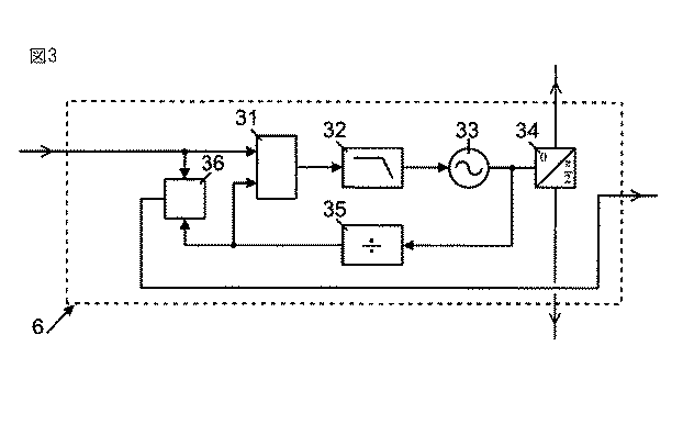
図3に詳細に示されるフロントエンドシンセサイザ6は、分数分周PLLシンセサイザである。 The front end synthesizer 6 shown in detail in FIG. 3 is a fractional frequency division PLL synthesizer.
チャージポンプを含む位相検出器として実装される位相検出器31は、固定された基準周波数frを有する基準信号をTCXO4から周期的に受信する第1入力と、第2入力とを有する。位相検出器31の出力は、ローパスフィルタであるループフィルタ32を介してVCO(Voltage-Controlled Oscillator、電圧制御発振器)33に接続される。VCO33によって生成されるシンセサイザ信号は、シンセサイザ周波数fsを有する周期的な信号であり、位相シフタ34によって2つの周期的なダウンコンバート信号に変換される。2つの周期的なダウンコンバート信号の周波数fdは、シンセサイザ信号の周波数fsの半分である。2つの周期的なダウンコンバート信号の一方は、2つの周期的なダウンコンバート信号の他方に対してπ/2すなわち90度シフトされる。また、2つの信号は、単一の複素ダウンコンバート信号として考えてもよい。上述のように、2つの周期的なダウンコンバート信号のそれぞれは、アナログミキサ9a及び9bの1つに供給される。また、VCO33の出力は、分周器35を有するフィードバックパスを介して位相検出器31の第2入力に接続される。
分周器35は分数分周器である。分周器35は、1よりも大きい分数の分周比Nfでシンセサイザ信号の周波数fsを分周して、分周信号を提供する。分周器35は、公知技術で構成され、N≧1であり且つL>Kである整数N、L、Kによって、KをN−1倍しL−KをN倍して、シンセサイザ信号の周波数を分周するように構成される。平均分周比は、N+K/L、すなわち(NL+K)/Lとなり、分数分周比、すなわち非整数分周比になる。具体的には、分周器35は、シグマ−デルタモジュレータで制御されてもよい。しかしながら、分数分周器35をどうように実装するかは重要ではない。多くの場合、分周信号(d)の周波数ffdと、シンセサイザ周波数fsとの関係は式(1)で示される。
(1) ffd = fs/Nf
The
(1) f fd = f s / Nf
アップダウンカウンタ36として実装されるサイクル検出器36は、位相検出器31の第1入力と並列にフロントエンドシンセサイザ6の入力に接続され、且つ分周器35の出力に接続される。フロントエンドシンセサイザ6のサイクルカウント出力において、アップダウンカウンタ36は、サイクルカウント信号を生成する。上述のように、生成されたサイクルカウント信号は、オフセット計算ユニット30に提供される。
A
図5は、いくつかのパラメータのタイミング図である。図5において、時間は(a)で示される基準信号の周期で測定される。なお、図5に示すタイミング図は一例であり、分周比及びGNSS回路で使用される他のパラメータを反映するものではない。 FIG. 5 is a timing diagram of several parameters. In FIG. 5, the time is measured in the period of the reference signal indicated by (a). Note that the timing diagram shown in FIG. 5 is an example and does not reflect the frequency division ratio and other parameters used in the GNSS circuit.
フロントエンドシンセサイザ6がロックされると、位相検出器31は、基準信号(a)の位相と分周信号(d)の位相との間の位相差が一定になるように、また好適にはゼロになるようにVCOを制御する。その結果として、分周信号(d)の周波数ffdは、基準信号(a)の周波数frと等しくなる。式(1)から式(2)が導かれる。
(2) fs = Nf・fr
When the front-end synthesizer 6 is locked, the
(2) f s = Nf · f r
この結果は、図5のロック状態期間Iに示される。 This result is shown in the lock state period I in FIG.
ロックが喪失すると、基準信号(a)の位相と分周信号(d)の位相との間の位相差が一定でなくなり変動し、図5のロック喪失期間IIに示すように、分周信号(d)の周波数は、基準信号(a)の周波数と異なるようになる(一例では大きくなる)。図5の第2ロック状態期間IIIに示すように、図5のロックが回復すると、シンセサイザ信号の周波数fsは式(2)の関係を満たす。しかしながら、ロック喪失期間IIの前方に位置するロック状態期間Iのシンセサイザ信号の部分と、ロック喪失期間IIの後方に位置するロック状態期間IIIのシンセサイザ信号の部分とは一般に同一の位相を有さない。これは、図5のシンセサイザ信号(b)と(c)とを比較することによって明らかになる。すなわち、シンセサイザ信号(c)は、ロック喪失期間IIによる影響を受けずに続いている仮想のシンセサイザ信号である。すなわち、シンセサイザ信号(c)は、ロック喪失が生じない場合のシンセサイザ信号である。実際のシンセサイザ信号(b)は、仮想のシンセサイザ信号(c)から位相オフセットψだけ異なっていることは明らかである。 When the lock is lost, the phase difference between the phase of the reference signal (a) and the frequency of the frequency-divided signal (d) becomes non-constant and fluctuates. As shown in the lock-loss period II in FIG. The frequency of d) becomes different from the frequency of the reference signal (a) (in one example, it becomes larger). As shown in the second lock state period III in FIG. 5, when the lock in FIG. 5 is restored, the frequency f s of the synthesizer signal satisfies the relationship of Expression (2). However, the portion of the synthesizer signal in the lock state period I located in front of the lock loss period II and the portion of the synthesizer signal in the lock state period III located behind the lock loss period II generally do not have the same phase. . This becomes clear by comparing the synthesizer signals (b) and (c) of FIG. That is, the synthesizer signal (c) is a virtual synthesizer signal that continues without being affected by the lock loss period II. That is, the synthesizer signal (c) is a synthesizer signal when no lock loss occurs. It is clear that the actual synthesizer signal (b) differs from the virtual synthesizer signal (c) by a phase offset ψ.
したがって、以下に詳細に説明するように、補正時間は、NCO29を適切に制御することによって位相オフセットを補償することが可能になるように決定される。このために、アップダウンカウンタ36は、図5の基準信号(a)及び分周信号(d)のサイクルに応答する。すなわち、アップダウンカウンタ36は、分周信号(d)の立ち上がりエッジを検出するとカウントアップし、基準信号(a)の立ち上がりエッジを検出するとカウントダウンする。フロントエッジシンセサイザ6が第1ロック状態期間Iの間にロックされている限り、基準信号(a)及び分周信号(d)のエッジは事実上一致している。したがって、信号(e)に示すように、アップダウンカウンタ36はゼロのままである。
Therefore, as will be described in detail below, the correction time is determined so that the phase offset can be compensated by appropriately controlling the NCO 29. For this purpose, the up / down
ロック喪失期間IIの間、分周信号(d)の立ち上がりエッジは、分周信号(d)の周波数が高くなるので、基準信号(a)の立ち上がりエッジに先行する。この結果、アップダウンカウンタ36は、分周信号(d)及び基準信号(a)の立ち上がりエッジを検知し、それに応じてアップダウンする。設定した時間の後、ロックが十分に回復する状態、すなわち、第2ロック状態期間IIIでは、基準信号(a)及び分周信号(d)のエッジは再び一致しているので、カウントは一定になる。カウントが安定することを使用して、ロック状態が回復したことを確認することができる。
During the lock loss period II, the rising edge of the divided signal (d) precedes the rising edge of the reference signal (a) because the frequency of the divided signal (d) is increased. As a result, the up / down
カウント(e)は、分周信号(d)のサイクルCfdの数と基準信号(a)のサイクルCrの数とのサイクル差Dを示す。すなわち、サイクル差Dは式(3)で示される。
(3) D = Cfd−Cr
Count (e) shows a cycle difference D between the number of cycles C r of the number of reference signal cycles C fd of the frequency-divided signal (d) (a). That is, the cycle difference D is expressed by equation (3).
(3) D = C fd −C r
ロック喪失期間IIの間に、サイクル差Dは増加する。サイクル差Dはサイクルカウント信号によって符号化される。 During the lock loss period II, the cycle difference D increases. The cycle difference D is encoded by a cycle count signal.
周波数の関係を示す式(1)は通常、シンセサイザがロックされているか否かに有効なので、ロック喪失の間の実際のシンセサイザ信号(b)と仮想のシンセサイザ信号(c)との間で増加する位相オフセットを反映するオフセット時間は、オフセット計算ユニット30において、式(4)のように決定できる。
(4) d = Nf・Dr
Equation (1) showing the frequency relationship is usually valid for whether or not the synthesizer is locked, so it increases between the actual synthesizer signal (b) and the virtual synthesizer signal (c) during the loss of lock. The offset time reflecting the phase offset can be determined by the offset calculation unit 30 as shown in Equation (4).
(4) d = Nf · D r
分周比及びロック喪失期間IIの端部におけるサイクル差によって生成される。 Generated by the division ratio and the cycle difference at the end of the lock loss period II.
シンセサイザ信号(b)の実際の位相オフセットψは、2πdである。この周波数がシンセサイザ信号(b)の周波数fsの半分の周波数であるため、ダウンコンバート信号の位相シフトがδ=ψ/2になるためである。 The actual phase offset ψ of the synthesizer signal (b) is 2πd. This is because this frequency is half the frequency f s of the synthesizer signal (b), so that the phase shift of the down-convert signal is δ = ψ / 2.
ダウンコンバート信号の周期性により、位相は、2πの余剰演算のみで規定されるので、位相シフトは、式(5)のように再度規定される。
(5) δ = mod(ψ/2,2π)
Due to the periodicity of the down-converted signal, the phase is defined only by a 2π surplus operation, so that the phase shift is defined again as shown in Equation (5).
(5) δ = mod (ψ / 2, 2π)
対応する補正時間−δは、オフセット計算ユニット30で計算される。以下で説明するように、対応する補正時間−δを使用して、NCO29を制御する。d/2の分数部に直接作用させることは、同等であり、且つより便利である。すなわち、
(6) d´ = mod(d/2,1)
The corresponding correction time −δ is calculated by the offset calculation unit 30. As described below, the NCO 29 is controlled using the corresponding correction time -δ. Directly acting on the fractional part of d / 2 is equivalent and more convenient. That is,
(6) d ′ = mod (d / 2, 1)
そして位相シフトは式(7)で示される。
(7) δ = 2πd´
The phase shift is expressed by equation (7).
(7) δ = 2πd ′
位相シフトが計算された後で、アップダウンカウンタ36はゼロにリセットされる。
After the phase shift is calculated, the up / down
図5に示す例において、分周比Nfは3.25であり、ロック喪失期間IIの分周信号(d)の立ち上がりエッジCfdの数は9であり、ロック喪失期間IIの基準信号(a)の立ち上がりエッジCrの数は4である。このため、ロック喪失期間IIの端部におけるサイクル差D(e)は5であり、オフセット時間d=Nf・Dは16.25である。これから、周期性、及びπ/4すなわち45度のダウンコンバート信号の位相シフトのためにπ/2すなわち90度に低減されるシンセサイザ信号の位相オフセットψは32.5πとなる。また、この結果は、式(6)を使用してより直接的に抽出できる。すなわち、d´=mod(d/2,1)=0.125及び式(7)により算出される。この補正時間は−π/4であり、位相シフトδの負である。 In the example shown in FIG. 5, the frequency division ratio Nf is 3.25, the number of rising edges C fd of the frequency division signal (d) in the lock loss period II is 9, and the reference signal (a the number of rising edges C r) of the 4. Therefore, the cycle difference D (e) at the end of the lock loss period II is 5, and the offset time d = Nf · D is 16.25. From this, the phase offset ψ of the synthesizer signal that is reduced to π / 2 or 90 degrees due to the periodicity and the phase shift of the down-converted signal of π / 4 or 45 degrees is 32.5π. This result can also be extracted more directly using equation (6). That is, d ′ = mod (d / 2, 1) = 0.125 and the equation (7). This correction time is −π / 4 and is negative of the phase shift δ.
分周信号の立ち上がりエッジでカウントダウンし、且つ基準信号の立ち上がりエッジでカウントアップするアップダウンカウンタを使用することができることは当然である。また、立ち下がりエッジで動作するアップダウンカウンタを使用してもよい。また、サイクル検出器は、アップダウンカウンタをサイクルカウンタとして使用する代わりに他の方法で実施してもよい。例えば、分周信号(d)のサイクルと基準信号(a)のサイクルとをそれぞれカウントする2つのアップカウンタを有してもよい。次いで、サイクルカウント信号は、双方のカウントの結果を符号化して、サイクル差Dは、オフセット計算ユニット30のロック喪失期間の端部におけるカウントの差として決定し、アップカウントがリセットされる。さらに、サイクル検出器は、分周信号及び基準信号の立ち上がりエッジ等を単に記憶し、記憶した情報をサイクル信号に符号化する単なるレジスタにしてもよい。実際のカウントはオフセット計算ユニットで実行してもよい。 Of course, it is possible to use an up / down counter that counts down at the rising edge of the divided signal and counts up at the rising edge of the reference signal. Further, an up / down counter that operates at a falling edge may be used. The cycle detector may be implemented in other ways instead of using the up / down counter as a cycle counter. For example, you may have two up counters which respectively count the cycle of the frequency-divided signal (d) and the cycle of the reference signal (a). The cycle count signal then encodes the results of both counts, the cycle difference D is determined as the difference in count at the end of the lock loss period of the offset calculation unit 30, and the upcount is reset. Further, the cycle detector may be a simple register that simply stores the divided signal, the rising edge of the reference signal, and the like, and encodes the stored information into the cycle signal. The actual count may be performed by an offset calculation unit.
アンテナ1で受信した対象とする信号の成分は式(8)で示される。
(8) S(t) = M(t)cos2πfct
The component of the target signal received by the
(8) S (t) = M (t) cos2πf c t
fcは搬送周波数を示し、M(t)は+1と−1の値である変調器符号化データである。アナログミキサ9a及び9bによるダウンコンバートは、変調器符号化データとフロントエンドシンセサイザ6で生成されるダウンコンバート信号cos2πfdt及びsin2πfdtとをそれぞれミックスし、複素アナログダウンコンバート信号を生成する。フィルタ10a及び10b並びに11a及び11bによるフィルタリングと、可変利得増幅器12a及び12bによる増幅と、A/D変換器15a及び15bによるA/D変換によって、複素デジタル中間信号を生じる。
(11) fi = fc−fd
f c indicates a carrier frequency, and M (t) is modulator encoded data having values of +1 and −1. Down-converted by the
(11) f i = f c −f d
中間周波数は、受信信号S(t)のキャリアと、絶対値1の複素定数によって乗算されるダウンコンバート信号との間の最初の位相シフトであってここでは無視される位相シフトとは異なる。
The intermediate frequency is the first phase shift between the carrier of the received signal S (t) and the down-converted signal multiplied by a complex constant of
第1ロック状態期間Iの間の中間信号が(10)で示され、ロック喪失期間IIの間のフロントエンドシンセサイザ6のロック喪失により位相オフセットψがシンセサイザ信号に取り込まれる場合、第2ロック状態期間IIIにおける中間信号は式(12)に示されるようになる。
ここで、δ=ψ/2は、位相オフセットにより生じるダウンコンバート信号の位相シフトである。 Here, δ = ψ / 2 is the phase shift of the down-conversion signal caused by the phase offset.
次いで、中間信号は、非回転信号、複素デジタル指数関数信号
(13) Sb I(t) = M(t)
The intermediate signal is then a non-rotating signal, a complex digital exponential signal
(13) S b I (t) = M (t)
そして、第2ロック状態期間IIIにおけるベースバンド信号部は式(14)に示す。
(14) Sb III(t) = M(t)eiδ
And the baseband signal part in the 2nd lock state period III is shown in Formula (14).
(14) S b III (t) = M (t) e iδ
この位相シフトを補償するために、式(4)、(6)及び(7)で示されるオフセット時間dから位相シフトδを計算したオフセット計算部30は第2ロック状態期間IIIの間に、複素ミキサ16に提供される非回転信号が、補正時間−δによって決定される位相補正に従うように、NCO29を制御する。ここで、中間信号は、ベースバンド信号部Sb IIIとeiδとを乗することによって得られる位相補正非回転信号
(15) Sb I´(t) = Sb I(t) = M(t)
In order to compensate for this phase shift, the offset calculation unit 30 that has calculated the phase shift δ from the offset time d expressed by the equations (4), (6), and (7) is complex during the second lock state period III. The NCO 29 is controlled so that the non-rotating signal provided to the
(15) S b I ′ (t) = S b I (t) = M (t)
第2ロック状態期間IIIの信号の補正部分は式(16)で示される。ここでは位相は一致している。
(16) Sb III´(t) = e-iδSb III(t) = M(t)
The correction part of the signal in the second lock state period III is expressed by equation (16). Here, the phases match.
(16) S b III '( t) = e -iδ S b III (t) = M (t)
ロック状態期間を分離するロック喪失事象のシーケンスがある場合、上述の位相補正は、全てのロック喪失期間の後に採用して、ロック状態期間に亘って位相が一致している位相補正ベースバンド信号を提供してもよい。NCO29及びミキサ16を上述のように使用することによって、位相シフトの補償が容易になる。しかしながら、位相補正を他の方法で実施してもよく、位相補正を信号処理工程のいくつかの点を変更することによって実施してもよいことは当然である。
If there is a sequence of lock loss events that separate the lock state periods, the above phase correction is employed after every lock loss period to obtain a phase correction baseband signal that is in phase over the lock state period. May be provided. Using the NCO 29 and the
図4は、本発明に係るシンセサイザの第2実施形態を示す図である。図4に示すシンセサイザは、信号処理装置の他の部分は適用し、図3のシンセサイザの変わりにフロントエンドシンセサイザとして使用して、GNSS受信器がGPS信号及びGLONASS信号を交互に使用できることになる。このため、フロントエンドシンセサイザ6´は、第1の分数分周器35aを有する第1フィードバックパスと、第2分数分周器35bを有する第2フィードバックパスとを有する。第2分周器35bの分周比Nfbは、第1分周器35aの分周比Nfaと相違する。第1分周器35aの出力と、フロントエンドシンセサイザ6´の入力とを接続する第1アップダウンカウンタ36aに加えて、第2分周器35bの出力と、フロントエンドシンセサイザ6´の入力とを接続する第2アップダウンカウンタ36bが提供される。このように、それぞれにフィードバックパスには対応するサイクルカウンタが含まれる。
FIG. 4 is a diagram showing a second embodiment of the synthesizer according to the present invention. The synthesizer shown in FIG. 4 applies the other parts of the signal processing apparatus, and can be used as a front-end synthesizer instead of the synthesizer of FIG. 3 so that the GNSS receiver can alternately use the GPS signal and the GLONASS signal. For this reason, the front-end synthesizer 6 ′ has a first feedback path having a first
フィードバックスイッチ37は、第1分周器35aの入力又は第2分周器35bの出力の何れかを、位相検出器31の第2入力に接続する。出力スイッチ38は、第1分周器35aの出力又は第2分周器35bの出力の何れかを、フロントエンドシンセサイザ6´の入力に接続して、オフセット計算ユニット30にサイクルカウント信号を提供する。
The
第1分周比Nfaを第1期間に最初に使用する場合、フィードバックスイッチ37は、第1分周器35aの出力を位相検出器31の第2入力に接続し、出力スイッチ38は、第1分周器35aの出力を、フロントエンドシンセサイザ6´の入力に接続する。第1フィードバックパスはロックされ、シンセサイザ信号の周波数fsはNfa・frに等しい。第2フィードバックパスはロック喪失状態である。
When using the first division ratio Nf a first in first period, the
第1期間が終了した後に、第2周比Nfbを第2期間に使用する場合、フィードバックスイッチ37は、第2分周器35bの出力を位相検出器31の第2入力に接続し、出力スイッチ38は、第2分周器35bの出力を、フロントエンドシンセサイザ6´の入力に接続する。設定時間が終了した後に、第2フィードバックパスはロックされ、第1フィードバックパスはロック喪失状態になる。第2サイクルカウンタのサイクル差Dbは、通常ゼロではなく、補正時間が計算し使用されることになるが、第2フィードバックパスが前に使用されていない場合にはその必要はない。
When the second frequency ratio Nf b is used for the second period after the first period ends, the
しかしながら、第2期間が終了した後に第1分周比Nfaを再度使用する場合、スイッチは先の状態に戻り、第1サイクルカウンタ36aのサイクル差Daは、オフセット時間及び補正時間を計算するためにオフセット計算ユニット30に提供される。計算されたオフセット時間及び補正時間をNCO29で使用して位相を補正して、第1期間のベースバンド信号の位相が一致する状態を確立する。
However, when the second period again using the first division ratio Nf a after finishing, the switch returns to the previous state, the cycle difference D a of the
このように、2つの異なる分周比Nfa及びNfbを有するフロントエンドシンセサイザ6´を交互に使用することにより、適切なフィードバックパスをそれぞれの場合に採用することになる。1つのフィードバックパスのみが一度にロックされる。したがって、ロック状態期間は、必然的に他のフィードバックパスのロック喪失期間になる。しかしながら、それぞれのフィードバックパスのロック喪失期間の間に形成される位相オフセットを計算し使用して、再びロックするときに位相が一致する状態を確立するので、分周比Nfa及びNfbそれぞれについて、対応するロック状態期間の全てに亘って位相が一致することになる。 Thus, by using the front-end synthesizer 6 'with two different division ratios Nf a and Nf b alternately it will employ the appropriate feedback path in each case. Only one feedback path is locked at a time. Therefore, the lock state period is necessarily a lock loss period of another feedback path. However, since the phase offset formed during the loss of lock period of each feedback path is calculated and used to establish a phase match when locking again, for each of the division ratios Nf a and Nf b , The phases will be consistent throughout the corresponding lock state period.
本発明の概念を2つ以上のフィードバックパスに拡張する方法は容易に理解されるので、本発明は、3つ以上の異なる分周比に交互に使用することは可能である。他のフィードバックバスがロックされているときはいずれも、所与のフィードバックパスのロックは維持できない。しかしながら、ロック喪失の間、対応するサイクルカウンタによってサイクルカウントが実行されているので、フィードバックパスが再び閉じてロックが回復するときはいつでも位相が一致する状態を速やかに確立できる。 Since it is easy to understand how to extend the concept of the present invention to more than one feedback path, the present invention can be used alternately for more than two different division ratios. The lock on a given feedback path cannot be maintained whenever the other feedback bus is locked. However, during the loss of lock, the cycle count is performed by the corresponding cycle counter so that a phase match can be quickly established whenever the feedback path closes again and lock is restored.
1 アンテナ
2 無線周波数部
3 バンドパスフィルタ
4 TCXO
5 ベースバンド部
6、6´ フロントエンドシンセサイザ
7 低雑音増幅器
8 制御可能RF増幅器
9a、9b アナログミキサ
10a、10b ハイパスフィルタ
11a、11b ローパスフィルタ
12a、12b 可変利得増幅器
13 ベースバンドシンセサイザ
14 分周器
15a、15b A/D変換器
16 デジタル複素ミキサ
17a、17b 周波数アナライザ
18 制御ユニット
19a、19b デシメーションフィルタ
20a、20b ダウンサンプラー
21 帯域消去ユニット
22 デジメータ
23 周波数アナライザ
24a、24b ダウンサンプラー
25 取得ユニット
26 トラッキングユニット
27 分周器
28 分周器
29 NCO
30 オフセット計算ユニット
31 位相検出器
32 ループフィルタ
33 VCO
34 位相シフタ
35a、35b 分周器
36a、36b サイクルカウンタ
37 フィードバックスイッチ
38 出力スイッチ
DESCRIPTION OF
DESCRIPTION OF
30 Offset
34
Claims (12)
前記ロック喪失期間(II)の間の前記基準信号のサイクル数と前記フィードバックパスの前記分周信号のサイクル数との間のサイクル差が評価され、前記フィードバックパスのシンセサイザ信号(b)のオフセット時間は、前記分周比と前記サイクル差とによる生成物に比例する数値として決定される、ことを特徴とする方法。 A fractional frequency division PLL during the second lock state period (III) after the lock loss period (II) with respect to the phase of the synthesizer signal during the first lock state period (I) before the lock loss period (II) In the method of determining the offset time of the synthesizer signal (b), during the lock state period (I and III), the synthesizer signal (b) is locked to the reference signal (a) by a feedback path, and the reference signal The phase relationship between the reference signal (a) and the frequency-divided signal (d) is kept constant so that the frequency of the signal (a) becomes equal to the frequency after frequency-dividing by the fractional frequency division ratio. A method,
A cycle difference between the number of cycles of the reference signal during the loss of lock period (II) and the number of cycles of the divided signal of the feedback path is evaluated, and the offset time of the synthesizer signal (b) of the feedback path Is determined as a numerical value proportional to the product due to the division ratio and the cycle difference.
前記アナログ入力信号は、前記シンセサイザ信号(b)から抽出されたダウンコンバート信号とミックスされることによりダウンコンバートされ、
前記ダウンコンバートされたアナログ信号は、デジタル信号に変換され、
前記位相補正デジタル信号は、前記デジタル信号から抽出され、前記抽出は、前記ロック喪失期間(II)の後に、補正時間が前記オフセット時間から抽出され、前記第2ロック状態期間(III)のデジタル信号の位相が前記補正時間に応じて補正されることを含む、請求項1に記載の方法。 The phase correction digital signal is an analog input such that the phase correction digital signal portion of the second lock state period (III) is in phase with the phase correction digital signal portion of the first lock state period (I). Generated from the signal,
The analog input signal is down-converted by being mixed with the down-convert signal extracted from the synthesizer signal (b),
The down-converted analog signal is converted into a digital signal,
The phase correction digital signal is extracted from the digital signal, and the extraction is extracted from the offset time after the lock loss period (II), and the digital signal of the second lock state period (III) The method according to claim 1, further comprising: correcting the phase of the input signal according to the correction time.
前記位相検出器により制御され、シンセサイザ信号(b)を生成する発振器と、
前記発振器の出力に接続される入力を備える分周器(35)であって、周波数が分数分周比で分周されたシンセサイザ信号(b)の周波数に等しい分周信号を出力で生成する分周器(35)を有し、前記分周器(35)の出力は、前記フィードバックパスを閉じるために前記位相検出器(31)の第2入力に接続され、又は接続可能にされるフィードバックパスと、を有する分数分周PLLシンセサイザであって、
前記位相検出器(31)の第1入力と、前記分周器(35)の出力とに接続され、前記基準信号(a)及び前記分周信号(d)のサイクルに応じて、前記分数分周PLLシンセサイザのサイクルカウント出力にサイクルカウント信号を提供するサイクル検出器を有する、請求項1〜5の何れか一項に記載の方法を実行する分数分周PLLシンセサイザ。 A phase detector (31) having a first input for receiving a periodic reference signal (a);
An oscillator controlled by the phase detector to generate a synthesizer signal (b);
A frequency divider (35) having an input connected to the output of the oscillator, wherein a frequency dividing signal equal to the frequency of the synthesizer signal (b) divided by a fractional frequency dividing ratio is generated at the output. A feedback path comprising a frequency divider (35), the output of the frequency divider (35) being connected to or made connectable to a second input of the phase detector (31) to close the feedback path A fractional frequency division PLL synthesizer comprising:
Connected to the first input of the phase detector (31) and the output of the frequency divider (35), depending on the cycle of the reference signal (a) and the frequency-divided signal (d), the fractional minutes 6. A fractional frequency division PLL synthesizer for performing the method of any one of claims 1-5, comprising a cycle detector that provides a cycle count signal to the cycle count output of the circumferential PLL synthesizer.
個々のフィードバックパスを閉じるために、前記位相検出器(31)の第2入力に前記分周器(35a、35b)の出力のそれぞれを交互に接続可能なフィードバックスイッチ(37)と、
フィードバックパスそれぞれにおいて、前記位相検出器(31)の第1入力と、前記分周器(35a、35b)の出力とに接続され、前記基準信号(a)と前記分周信号(d)とに応答するサイクル検出器と、
前記分数分周PLLシンセサイザのサイクルカウント出力に前記サイクル検出器の出力を交互に接続可能な出力スイッチ(38)と、を有する、請求項6〜8の何れか一項に記載の分数分周PLLシンセサイザ。 A frequency divider (35a, 35b) having an input connected to the output of the oscillator, wherein the frequency is the frequency of the synthesizer signal divided by a non-integer division ratio (Nfa, Nfb) specific to the feedback path. Two or more feedback paths each having a frequency divider that generates an associated frequency-divided signal at the output;
A feedback switch (37) capable of alternately connecting each of the outputs of the frequency dividers (35a, 35b) to a second input of the phase detector (31) to close the individual feedback paths;
In each feedback path, the first input of the phase detector (31) and the output of the frequency divider (35a, 35b) are connected to the reference signal (a) and the frequency-divided signal (d). A responding cycle detector;
The fractional frequency division PLL according to any one of claims 6 to 8, further comprising: an output switch (38) capable of alternately connecting the output of the cycle detector to a cycle count output of the fractional frequency division PLL synthesizer. Synthesizer .
複素ダウンコンバートアナログ信号をアナログ入力信号から抽出するために、前記第1ダウンコンバート信号を受信する第1アナログミキサ(9a)及び前記第2ダウンコンバート信号を受信する第2アナログミキサ(9b)と、
複素デジタル中間信号を前記複素ダウンコンバートアナログ信号から抽出するA/D変換器(15a、15b)と、
前記サイクルカウント信号に依存する補正時間に従って位相補正がされる複素デジタル指数を提供するように構成されるNCO(29)によって制御される複素ミキサ(16)と、を更に有する、信号処理装置。 A signal processing apparatus having a fractional frequency division PLL synthesizer according as the front end synthesizer (6, 6 ') in claim 8 or 8 and 9,
The complex down-conversion analog signals in order to extract from the analog input signal, said first analog mixer (9a) and a second analog mixer for receiving the second down-converted signal to the first receiving downconverted signal and (9b),
An A / D converter (15a, 15b) for extracting a complex digital intermediate signal from the complex down-converted analog signal;
And a complex mixer (16) controlled by an NCO (29) configured to provide a complex digital exponent that is phase-corrected according to a correction time dependent on the cycle count signal.
Applications Claiming Priority (2)
| Application Number | Priority Date | Filing Date | Title |
|---|---|---|---|
| EP12405002.2 | 2012-01-06 | ||
| EP20120405002 EP2613442B1 (en) | 2012-01-06 | 2012-01-06 | A method for determining an offset term for a fractional-N PLL synthesizer signal, a synthesizer for carrying out the method, a signal processing device and a GNSS receiver |
Publications (2)
| Publication Number | Publication Date |
|---|---|
| JP2013143773A JP2013143773A (en) | 2013-07-22 |
| JP6110141B2 true JP6110141B2 (en) | 2017-04-05 |
Family
ID=45562928
Family Applications (1)
| Application Number | Title | Priority Date | Filing Date |
|---|---|---|---|
| JP2013000066A Active JP6110141B2 (en) | 2012-01-06 | 2013-01-04 | Method for determining offset time of fractional frequency division PLL synthesizer signal, and synthesizer, signal processing apparatus and GNSS receiver for executing the method |
Country Status (4)
| Country | Link |
|---|---|
| US (1) | US8644783B2 (en) |
| EP (1) | EP2613442B1 (en) |
| JP (1) | JP6110141B2 (en) |
| CN (1) | CN103199858B (en) |
Families Citing this family (9)
| Publication number | Priority date | Publication date | Assignee | Title |
|---|---|---|---|---|
| US8692594B2 (en) * | 2011-12-19 | 2014-04-08 | Ati Technologies Ulc | Phase-locked loop frequency stepping |
| US9618625B2 (en) | 2012-07-06 | 2017-04-11 | Apple Inc. | System and method for continuous carrier wave reconstruction |
| US9360557B1 (en) | 2012-07-06 | 2016-06-07 | Apple Inc. | Systems, methods, devices and subassemblies for rapid-acquisition access to high-precision positioning, navigation and/or timing solutions |
| WO2015153335A1 (en) * | 2014-04-03 | 2015-10-08 | Coherent Navigation, Inc. | System and method for continuous carrier wave reconstruction |
| CN105915216B (en) * | 2016-04-06 | 2019-01-25 | 上海交通大学 | LO decimal frequency divider is adjusted in medium-high frequency multimode frequency dividing ratio |
| US10965027B2 (en) * | 2017-09-20 | 2021-03-30 | Kymeta Corporation | RF ripple correction in an antenna aperture |
| WO2019075414A1 (en) | 2017-10-12 | 2019-04-18 | Synaptics Incorporated | Phase locked loop sampler and restorer |
| US11601307B2 (en) | 2018-12-17 | 2023-03-07 | U-Blox Ag | Estimating one or more characteristics of a communications channel |
| CN114070308B (en) * | 2022-01-17 | 2022-11-22 | 中国电子科技集团公司第二十九研究所 | Broadband low-phase-noise frequency synthesis circuit |
Family Cites Families (19)
| Publication number | Priority date | Publication date | Assignee | Title |
|---|---|---|---|---|
| JPH0774626A (en) * | 1993-09-01 | 1995-03-17 | Fujitsu Ltd | Pll circuit |
| FR2763196B1 (en) | 1997-05-07 | 1999-07-30 | Thomson Csf | CONSISTENT FREQUENCY SYNTHESIZER WITH PHASE LOOP AND NOT FRACTIONAL |
| WO1999013582A1 (en) * | 1997-09-09 | 1999-03-18 | Advanced Fibre Communications, Inc. | Perturbation tolerant digital phase-locked loop employing phase-frequency detector |
| JPH11225072A (en) * | 1998-02-05 | 1999-08-17 | Fujitsu Ltd | Spurious suppressing device, its method and fractional n synthesizer |
| US6914935B2 (en) * | 2001-02-21 | 2005-07-05 | Freescale Semiconductor, Inc. | Fractional N synthesizer with reduced fractionalization spurs |
| US6456164B1 (en) * | 2001-03-05 | 2002-09-24 | Koninklijke Philips Electronics N.V. | Sigma delta fractional-N frequency divider with improved noise and spur performance |
| US7003065B2 (en) * | 2001-03-09 | 2006-02-21 | Ericsson Inc. | PLL cycle slip detection |
| US6553089B2 (en) * | 2001-03-20 | 2003-04-22 | Gct Semiconductor, Inc. | Fractional-N frequency synthesizer with fractional compensation method |
| US6556086B2 (en) * | 2001-05-31 | 2003-04-29 | Analog Devices, Inc. | Fractional-N synthesizer and method of synchronization of the output phase |
| US6556082B1 (en) | 2001-10-12 | 2003-04-29 | Eic Corporation | Temperature compensated current mirror |
| US6823033B2 (en) * | 2002-03-12 | 2004-11-23 | Qualcomm Inc. | ΣΔdelta modulator controlled phase locked loop with a noise shaped dither |
| KR100475091B1 (en) * | 2002-08-30 | 2005-03-10 | 삼성전자주식회사 | Data slicer and Data slicing method in optical disc system |
| US7463710B2 (en) | 2003-06-27 | 2008-12-09 | Analog Devices, Inc. | Fractional-N synthesizer and method of programming the output phase |
| KR100990484B1 (en) * | 2004-03-29 | 2010-10-29 | 삼성전자주식회사 | Transmission clock signal generator for serial bus communication |
| WO2007091516A1 (en) * | 2006-02-07 | 2007-08-16 | Mitsubishi Electric Corporation | Phase synchronization loop type frequency synthesizer of fractional n-type, and phase shift circuit with frequency converting function |
| JP4649362B2 (en) * | 2006-04-19 | 2011-03-09 | 株式会社東芝 | Oscillator control device |
| US20090224974A1 (en) | 2008-03-04 | 2009-09-10 | Navasic Corporation | Power efficient global positioning system receiver |
| US8368480B2 (en) * | 2009-06-24 | 2013-02-05 | Mediatek Inc. | Phase locked loop circuits and gain calibration methods thereof |
| CN101741380B (en) * | 2009-12-22 | 2014-07-30 | 北京中星微电子有限公司 | Method and system for locking detection of phase-locked loop and phase-locked loop circuit |
-
2012
- 2012-01-06 EP EP20120405002 patent/EP2613442B1/en active Active
- 2012-03-19 US US13/424,245 patent/US8644783B2/en active Active
- 2012-12-26 CN CN201210575334.2A patent/CN103199858B/en active Active
-
2013
- 2013-01-04 JP JP2013000066A patent/JP6110141B2/en active Active
Also Published As
| Publication number | Publication date |
|---|---|
| EP2613442B1 (en) | 2015-05-13 |
| CN103199858A (en) | 2013-07-10 |
| US20130176059A1 (en) | 2013-07-11 |
| CN103199858B (en) | 2017-05-31 |
| EP2613442A1 (en) | 2013-07-10 |
| JP2013143773A (en) | 2013-07-22 |
| US8644783B2 (en) | 2014-02-04 |
Similar Documents
| Publication | Publication Date | Title |
|---|---|---|
| JP6110141B2 (en) | Method for determining offset time of fractional frequency division PLL synthesizer signal, and synthesizer, signal processing apparatus and GNSS receiver for executing the method | |
| US10236923B2 (en) | Method of processing a digital signal derived from an analog input signal of a GNSS receiver, a GNSS receiver base band circuit for carrying out the method and a GNSS receiver | |
| JP4955769B2 (en) | Reference signal generation for multiple communication systems | |
| US8229460B2 (en) | Demodulation apparatus and receiving apparatus | |
| EP3701631B1 (en) | Digital-to-time converter (dtc) assisted all digital phase locked loop (adpll) circuit | |
| US20030186666A1 (en) | Frequency-timing control loop for wireless communication systems | |
| KR101030950B1 (en) | Dual mode satellite signal receiver and method thereof | |
| US20120069884A1 (en) | Digital phase detector and digital phase-locked loop | |
| WO2017052876A1 (en) | Calibration of dynamic error in high resolution digital-to-time converters | |
| WO1999057929A1 (en) | Gsm cellular telephone and gps receiver combination | |
| US8280330B2 (en) | Crystal-less clock generation for radio frequency receivers | |
| US7573348B2 (en) | Arrangement and method for determining a gradient factor for a digitally controlled oscillator, and phase locked loop | |
| US9791574B2 (en) | Method and system for repurposing of a global navigation satellite system receiver for receiving low-earth orbit communication satellite signals | |
| US20160025861A1 (en) | Method and system for indoor global navigation satellite system detection utilizing low-earth orbit satellite signals | |
| US8489053B2 (en) | Compensation of local oscillator phase jitter | |
| US20060279365A1 (en) | Digital phase locked loop and method for correcting interference components in a phase locked loop | |
| US9194956B2 (en) | Amelioration of frequency errors and/or their effects | |
| US20130187810A1 (en) | Method And System For An Embedded And Hosted Architecture For A Medium Earth Orbit Satellite And Low Earth Orbit Satellite Positioning Engine | |
| RU2159448C1 (en) | Device for receiving signals from satellite radio navigation systems | |
| JP2013026969A (en) | Radio receiver |
Legal Events
| Date | Code | Title | Description |
|---|---|---|---|
| A621 | Written request for application examination |
Free format text: JAPANESE INTERMEDIATE CODE: A621 Effective date: 20151113 |
|
| A977 | Report on retrieval |
Free format text: JAPANESE INTERMEDIATE CODE: A971007 Effective date: 20160815 |
|
| A131 | Notification of reasons for refusal |
Free format text: JAPANESE INTERMEDIATE CODE: A131 Effective date: 20160830 |
|
| A601 | Written request for extension of time |
Free format text: JAPANESE INTERMEDIATE CODE: A601 Effective date: 20161129 |
|
| A521 | Request for written amendment filed |
Free format text: JAPANESE INTERMEDIATE CODE: A523 Effective date: 20170120 |
|
| TRDD | Decision of grant or rejection written | ||
| A01 | Written decision to grant a patent or to grant a registration (utility model) |
Free format text: JAPANESE INTERMEDIATE CODE: A01 Effective date: 20170207 |
|
| A61 | First payment of annual fees (during grant procedure) |
Free format text: JAPANESE INTERMEDIATE CODE: A61 Effective date: 20170309 |
|
| R150 | Certificate of patent or registration of utility model |
Ref document number: 6110141 Country of ref document: JP Free format text: JAPANESE INTERMEDIATE CODE: R150 |
|
| S533 | Written request for registration of change of name |
Free format text: JAPANESE INTERMEDIATE CODE: R313533 |
|
| R350 | Written notification of registration of transfer |
Free format text: JAPANESE INTERMEDIATE CODE: R350 |
|
| R250 | Receipt of annual fees |
Free format text: JAPANESE INTERMEDIATE CODE: R250 |
|
| R250 | Receipt of annual fees |
Free format text: JAPANESE INTERMEDIATE CODE: R250 |
|
| R250 | Receipt of annual fees |
Free format text: JAPANESE INTERMEDIATE CODE: R250 |
|
| R250 | Receipt of annual fees |
Free format text: JAPANESE INTERMEDIATE CODE: R250 |
|
| R250 | Receipt of annual fees |
Free format text: JAPANESE INTERMEDIATE CODE: R250 |