US10965027B2 - RF ripple correction in an antenna aperture - Google Patents
RF ripple correction in an antenna aperture Download PDFInfo
- Publication number
- US10965027B2 US10965027B2 US16/134,197 US201816134197A US10965027B2 US 10965027 B2 US10965027 B2 US 10965027B2 US 201816134197 A US201816134197 A US 201816134197A US 10965027 B2 US10965027 B2 US 10965027B2
- Authority
- US
- United States
- Prior art keywords
- antenna
- ripple
- voltage
- array
- voltages
- Prior art date
- Legal status (The legal status is an assumption and is not a legal conclusion. Google has not performed a legal analysis and makes no representation as to the accuracy of the status listed.)
- Active, expires
Links
- 238000012937 correction Methods 0.000 title claims abstract description 105
- 239000004973 liquid crystal related substance Substances 0.000 claims abstract description 136
- 238000000034 method Methods 0.000 claims abstract description 90
- 238000012360 testing method Methods 0.000 claims description 43
- 230000004044 response Effects 0.000 claims description 23
- 238000005259 measurement Methods 0.000 claims description 13
- 230000015654 memory Effects 0.000 claims description 9
- 230000007613 environmental effect Effects 0.000 claims description 5
- 238000012545 processing Methods 0.000 description 67
- 230000008569 process Effects 0.000 description 48
- 210000000554 iris Anatomy 0.000 description 38
- 210000004027 cell Anatomy 0.000 description 37
- 230000003287 optical effect Effects 0.000 description 29
- 239000004020 conductor Substances 0.000 description 24
- 230000005540 biological transmission Effects 0.000 description 23
- 239000000758 substrate Substances 0.000 description 23
- 239000011521 glass Substances 0.000 description 17
- 238000004891 communication Methods 0.000 description 15
- 239000011159 matrix material Substances 0.000 description 15
- 239000002184 metal Substances 0.000 description 15
- 229910052751 metal Inorganic materials 0.000 description 15
- 230000008859 change Effects 0.000 description 14
- 125000006850 spacer group Chemical group 0.000 description 13
- 238000010586 diagram Methods 0.000 description 11
- 230000005284 excitation Effects 0.000 description 8
- 230000007704 transition Effects 0.000 description 8
- 230000003247 decreasing effect Effects 0.000 description 7
- 238000003491 array Methods 0.000 description 6
- 239000003990 capacitor Substances 0.000 description 6
- 230000000694 effects Effects 0.000 description 6
- 239000000463 material Substances 0.000 description 6
- 230000000295 complement effect Effects 0.000 description 5
- 230000008878 coupling Effects 0.000 description 5
- 238000010168 coupling process Methods 0.000 description 5
- 238000005859 coupling reaction Methods 0.000 description 5
- 230000007423 decrease Effects 0.000 description 5
- 230000010287 polarization Effects 0.000 description 5
- 238000009825 accumulation Methods 0.000 description 4
- 230000001066 destructive effect Effects 0.000 description 4
- 230000006870 function Effects 0.000 description 4
- 230000007246 mechanism Effects 0.000 description 4
- 230000000737 periodic effect Effects 0.000 description 4
- 230000005855 radiation Effects 0.000 description 4
- 238000013459 approach Methods 0.000 description 3
- 230000015556 catabolic process Effects 0.000 description 3
- 238000006243 chemical reaction Methods 0.000 description 3
- 238000006731 degradation reaction Methods 0.000 description 3
- 230000001419 dependent effect Effects 0.000 description 3
- 238000013461 design Methods 0.000 description 3
- 238000005516 engineering process Methods 0.000 description 3
- 238000013507 mapping Methods 0.000 description 3
- 239000000203 mixture Substances 0.000 description 3
- 230000009467 reduction Effects 0.000 description 3
- 239000010409 thin film Substances 0.000 description 3
- RYGMFSIKBFXOCR-UHFFFAOYSA-N Copper Chemical compound [Cu] RYGMFSIKBFXOCR-UHFFFAOYSA-N 0.000 description 2
- 239000006096 absorbing agent Substances 0.000 description 2
- 238000004590 computer program Methods 0.000 description 2
- 238000011109 contamination Methods 0.000 description 2
- 229910052802 copper Inorganic materials 0.000 description 2
- 239000010949 copper Substances 0.000 description 2
- 238000001093 holography Methods 0.000 description 2
- 238000004519 manufacturing process Methods 0.000 description 2
- 230000004048 modification Effects 0.000 description 2
- 238000012986 modification Methods 0.000 description 2
- 230000009897 systematic effect Effects 0.000 description 2
- 230000009471 action Effects 0.000 description 1
- 230000004075 alteration Effects 0.000 description 1
- 230000003321 amplification Effects 0.000 description 1
- 230000008901 benefit Effects 0.000 description 1
- 230000015572 biosynthetic process Effects 0.000 description 1
- 239000000470 constituent Substances 0.000 description 1
- 239000000356 contaminant Substances 0.000 description 1
- 230000001808 coupling effect Effects 0.000 description 1
- 210000002858 crystal cell Anatomy 0.000 description 1
- 239000007857 degradation product Substances 0.000 description 1
- 238000001514 detection method Methods 0.000 description 1
- 230000005684 electric field Effects 0.000 description 1
- 238000001914 filtration Methods 0.000 description 1
- 239000006260 foam Substances 0.000 description 1
- -1 for example Substances 0.000 description 1
- AMGQUBHHOARCQH-UHFFFAOYSA-N indium;oxotin Chemical compound [In].[Sn]=O AMGQUBHHOARCQH-UHFFFAOYSA-N 0.000 description 1
- 238000002955 isolation Methods 0.000 description 1
- 238000005297 material degradation process Methods 0.000 description 1
- 238000001465 metallisation Methods 0.000 description 1
- 238000003199 nucleic acid amplification method Methods 0.000 description 1
- 150000007524 organic acids Chemical class 0.000 description 1
- 235000005985 organic acids Nutrition 0.000 description 1
- 238000012856 packing Methods 0.000 description 1
- 230000002085 persistent effect Effects 0.000 description 1
- 230000000644 propagated effect Effects 0.000 description 1
- 230000001902 propagating effect Effects 0.000 description 1
- 230000004043 responsiveness Effects 0.000 description 1
- 230000011218 segmentation Effects 0.000 description 1
- 230000035945 sensitivity Effects 0.000 description 1
- 238000000926 separation method Methods 0.000 description 1
- 230000008054 signal transmission Effects 0.000 description 1
- 239000000126 substance Substances 0.000 description 1
- 230000002459 sustained effect Effects 0.000 description 1
- 208000024891 symptom Diseases 0.000 description 1
- 230000036962 time dependent Effects 0.000 description 1
- 230000009466 transformation Effects 0.000 description 1
Images


Classifications
-
- H—ELECTRICITY
- H01—ELECTRIC ELEMENTS
- H01Q—ANTENNAS, i.e. RADIO AERIALS
- H01Q3/00—Arrangements for changing or varying the orientation or the shape of the directional pattern of the waves radiated from an antenna or antenna system
- H01Q3/26—Arrangements for changing or varying the orientation or the shape of the directional pattern of the waves radiated from an antenna or antenna system varying the relative phase or relative amplitude of energisation between two or more active radiating elements; varying the distribution of energy across a radiating aperture
- H01Q3/28—Arrangements for changing or varying the orientation or the shape of the directional pattern of the waves radiated from an antenna or antenna system varying the relative phase or relative amplitude of energisation between two or more active radiating elements; varying the distribution of energy across a radiating aperture varying the amplitude
-
- H—ELECTRICITY
- H01—ELECTRIC ELEMENTS
- H01Q—ANTENNAS, i.e. RADIO AERIALS
- H01Q21/00—Antenna arrays or systems
- H01Q21/06—Arrays of individually energised antenna units similarly polarised and spaced apart
- H01Q21/061—Two dimensional planar arrays
- H01Q21/064—Two dimensional planar arrays using horn or slot aerials
-
- G—PHYSICS
- G01—MEASURING; TESTING
- G01R—MEASURING ELECTRIC VARIABLES; MEASURING MAGNETIC VARIABLES
- G01R29/00—Arrangements for measuring or indicating electric quantities not covered by groups G01R19/00 - G01R27/00
- G01R29/08—Measuring electromagnetic field characteristics
- G01R29/10—Radiation diagrams of antennas
-
- H—ELECTRICITY
- H01—ELECTRIC ELEMENTS
- H01Q—ANTENNAS, i.e. RADIO AERIALS
- H01Q1/00—Details of, or arrangements associated with, antennas
- H01Q1/36—Structural form of radiating elements, e.g. cone, spiral, umbrella; Particular materials used therewith
- H01Q1/38—Structural form of radiating elements, e.g. cone, spiral, umbrella; Particular materials used therewith formed by a conductive layer on an insulating support
-
- H—ELECTRICITY
- H01—ELECTRIC ELEMENTS
- H01Q—ANTENNAS, i.e. RADIO AERIALS
- H01Q13/00—Waveguide horns or mouths; Slot antennas; Leaky-waveguide antennas; Equivalent structures causing radiation along the transmission path of a guided wave
- H01Q13/10—Resonant slot antennas
- H01Q13/103—Resonant slot antennas with variable reactance for tuning the antenna
-
- H—ELECTRICITY
- H01—ELECTRIC ELEMENTS
- H01Q—ANTENNAS, i.e. RADIO AERIALS
- H01Q17/00—Devices for absorbing waves radiated from an antenna; Combinations of such devices with active antenna elements or systems
- H01Q17/001—Devices for absorbing waves radiated from an antenna; Combinations of such devices with active antenna elements or systems for modifying the directional characteristic of an aerial
-
- H—ELECTRICITY
- H01—ELECTRIC ELEMENTS
- H01Q—ANTENNAS, i.e. RADIO AERIALS
- H01Q21/00—Antenna arrays or systems
- H01Q21/0006—Particular feeding systems
- H01Q21/0012—Radial guide fed arrays
-
- H—ELECTRICITY
- H01—ELECTRIC ELEMENTS
- H01Q—ANTENNAS, i.e. RADIO AERIALS
- H01Q21/00—Antenna arrays or systems
- H01Q21/06—Arrays of individually energised antenna units similarly polarised and spaced apart
- H01Q21/061—Two dimensional planar arrays
- H01Q21/065—Patch antenna array
-
- H—ELECTRICITY
- H01—ELECTRIC ELEMENTS
- H01Q—ANTENNAS, i.e. RADIO AERIALS
- H01Q3/00—Arrangements for changing or varying the orientation or the shape of the directional pattern of the waves radiated from an antenna or antenna system
- H01Q3/005—Arrangements for changing or varying the orientation or the shape of the directional pattern of the waves radiated from an antenna or antenna system using remotely controlled antenna positioning or scanning
-
- H—ELECTRICITY
- H01—ELECTRIC ELEMENTS
- H01Q—ANTENNAS, i.e. RADIO AERIALS
- H01Q3/00—Arrangements for changing or varying the orientation or the shape of the directional pattern of the waves radiated from an antenna or antenna system
- H01Q3/24—Arrangements for changing or varying the orientation or the shape of the directional pattern of the waves radiated from an antenna or antenna system varying the orientation by switching energy from one active radiating element to another, e.g. for beam switching
- H01Q3/247—Arrangements for changing or varying the orientation or the shape of the directional pattern of the waves radiated from an antenna or antenna system varying the orientation by switching energy from one active radiating element to another, e.g. for beam switching by switching different parts of a primary active element
-
- H—ELECTRICITY
- H01—ELECTRIC ELEMENTS
- H01Q—ANTENNAS, i.e. RADIO AERIALS
- H01Q3/00—Arrangements for changing or varying the orientation or the shape of the directional pattern of the waves radiated from an antenna or antenna system
- H01Q3/26—Arrangements for changing or varying the orientation or the shape of the directional pattern of the waves radiated from an antenna or antenna system varying the relative phase or relative amplitude of energisation between two or more active radiating elements; varying the distribution of energy across a radiating aperture
- H01Q3/30—Arrangements for changing or varying the orientation or the shape of the directional pattern of the waves radiated from an antenna or antenna system varying the relative phase or relative amplitude of energisation between two or more active radiating elements; varying the distribution of energy across a radiating aperture varying the relative phase between the radiating elements of an array
- H01Q3/34—Arrangements for changing or varying the orientation or the shape of the directional pattern of the waves radiated from an antenna or antenna system varying the relative phase or relative amplitude of energisation between two or more active radiating elements; varying the distribution of energy across a radiating aperture varying the relative phase between the radiating elements of an array by electrical means
- H01Q3/36—Arrangements for changing or varying the orientation or the shape of the directional pattern of the waves radiated from an antenna or antenna system varying the relative phase or relative amplitude of energisation between two or more active radiating elements; varying the distribution of energy across a radiating aperture varying the relative phase between the radiating elements of an array by electrical means with variable phase-shifters
-
- H—ELECTRICITY
- H03—ELECTRONIC CIRCUITRY
- H03D—DEMODULATION OR TRANSFERENCE OF MODULATION FROM ONE CARRIER TO ANOTHER
- H03D3/00—Demodulation of angle-, frequency- or phase- modulated oscillations
- H03D3/007—Demodulation of angle-, frequency- or phase- modulated oscillations by converting the oscillations into two quadrature related signals
- H03D3/008—Compensating DC offsets
-
- G—PHYSICS
- G01—MEASURING; TESTING
- G01R—MEASURING ELECTRIC VARIABLES; MEASURING MAGNETIC VARIABLES
- G01R29/00—Arrangements for measuring or indicating electric quantities not covered by groups G01R19/00 - G01R27/00
- G01R29/08—Measuring electromagnetic field characteristics
- G01R29/0864—Measuring electromagnetic field characteristics characterised by constructional or functional features
- G01R29/0892—Details related to signal analysis or treatment; presenting results, e.g. displays; measuring specific signal features other than field strength, e.g. polarisation, field modes, phase, envelope, maximum value
-
- G—PHYSICS
- G01—MEASURING; TESTING
- G01R—MEASURING ELECTRIC VARIABLES; MEASURING MAGNETIC VARIABLES
- G01R31/00—Arrangements for testing electric properties; Arrangements for locating electric faults; Arrangements for electrical testing characterised by what is being tested not provided for elsewhere
- G01R31/28—Testing of electronic circuits, e.g. by signal tracer
- G01R31/282—Testing of electronic circuits specially adapted for particular applications not provided for elsewhere
- G01R31/2822—Testing of electronic circuits specially adapted for particular applications not provided for elsewhere of microwave or radiofrequency circuits
Definitions
- Embodiments of the present invention relate to the field of radio frequency (RF) devices having liquid crystals (LCs); more particularly, embodiments of the present invention relate to the driving and control of radio frequency (RF) devices having liquid crystals (LCs) for which RF ripple, flicker or other observations have been made.
- RF radio frequency
- Display devices using liquid crystals typically use a drive method that inverts the polarity of the drive voltage applied across the LC at regular intervals. These intervals are typically called time frames or frames. This is done to prevent or minimize trapping of charges within the LC device that can result in a storage of a voltage within the LC device. These charges arise from numerous sources, mostly coming from contamination or a degradation of materials in the LC device. A persistent application of a given polarity separates the charges of contaminants (such as organic acids), and moves them to the boundaries of the LC device, where they may stick. By inverting the polarity of the applied voltage, the separation and transport of these charged species can be reduced. However, inverting the voltage symmetrically is difficult to do, and thus a “net DC offset” results.
- LC liquid crystals
- a condition called “flicker” can also occur, which is caused when there is a sufficient difference between the absolute value of the voltage applied during a positive frame and that applied during a negative frame such that the optical properties of the LC in positive and negative frames are different and visible by a human eye. In a display, these may be seen or detected by a light sensing device. Over time, the asymmetry between the positive and negative frames that caused flicker results in storage charge. Stored charge within the device can create differences between the voltage that is intended to be applied to the LC, and the voltage that is actually applied. This can result in a reduction in the root mean squared (RMS) voltage applied to the elements.
- RMS root mean squared
- Another symptom of this problem referred to herein as “image sticking”, can occur, which is an influence of a previously applied image pattern upon the next image pattern.
- the DC offset between the absolute value of voltage applied to the LC device during the one interval of the drive polarity and the absolute value of the voltage applied during the next interval of opposite drive polarity be as close to zero as possible.
- adjustment of the DC offset may be done by compensating the voltage value sent to each element for each polarity at every gray level.
- the amount of the compensation voltage at each polarity at chosen gray levels may be determined optically and is selected to null the flicker. That is, a voltage difference between the positive and negative polarity of frames results in an optical flicker, which can be observed by an optical sensor or array of sensors (camera) and nulled using a correction algorithm in an automated test setup. Then, those correction values can be stored and used for minimizing the offset.
- a DC offset problem is described above for LC displays.
- the same phenomenon is observed in LC RF antenna since LC driving mechanism is the same as displays.
- the effect of this phenomenon is observed as RF ripple in the antenna performance which degrades the carrier to noise (C/N) ratio at the receiver.
- DC offset correction methods used in LC displays cannot be applied to the current state of the LC RF antenna because the antenna structure blocks the path for optical measurements of the LC response.
- the antenna comprises: an array of antenna elements having liquid crystal (LC); drive circuitry coupled to the array and having a plurality of drivers, each driver of the plurality of drivers coupled to an antenna element of the array and operable to apply a drive voltage to the antenna element; and radio-frequency (RF) ripple correction logic coupled to the drive circuitry to adjust drive voltages to compensate for ripple.
- LC liquid crystal
- RF radio-frequency
- FIG. 1 is a block diagram of one embodiment of voltage adjustment apparatus.
- FIG. 2 illustrates the transmission parameter S 21 over time without radio-frequency (RF) ripple.
- FIG. 3 illustrates the transmission parameter S 21 over time with RF ripple.
- FIG. 4 illustrates driving voltages for an RF unit cell in an LC antenna aperture.
- FIG. 5 illustrates data (source) driver output control using gamma voltages.
- FIG. 6 is a flow diagram of an embodiment of a RF ripple correction process.
- FIGS. 7A and 7D illustrate an example of voltage adjustments using one embodiment of the RF ripple correction process.
- FIG. 8 is a flow diagram of another embodiment of a RF ripple correction process.
- FIG. 9 illustrates an example of a transmission versus voltage curve.
- FIG. 10 is a flow diagram of a one embodiment of a process to determine DC offset correction values.
- FIG. 11 illustrates one embodiment of routing for a single test structure located outside of the waveguide area.
- FIG. 12 illustrates one embodiment of a test structure.
- FIG. 13 illustrates one example of gate and source line routing for optically transparent test structures.
- FIGS. 14 and 15 illustrate examples of patch glass (substrate) and iris glass (substrate) structures, respectively, that form the patch and iris for the antenna aperture.
- FIGS. 16 and 17 illustrate examples of routing on the patch glass substrate and iris glass substrate, respectively.
- FIG. 18 illustrates the schematic of one embodiment of a cylindrically fed holographic radial aperture antenna.
- FIG. 19 illustrates a perspective view of one row of antenna elements that includes a ground plane and a reconfigurable resonator layer.
- FIG. 20 illustrates one embodiment of a tunable resonator/slot.
- FIG. 21 illustrates a cross section view of one embodiment of a physical antenna aperture.
- FIGS. 22A-D illustrate one embodiment of the different layers for creating the slotted array.
- FIG. 23 illustrates a side view of one embodiment of a cylindrically fed antenna structure.
- FIG. 24 illustrates another embodiment of the antenna system with an outgoing wave.
- FIG. 25 illustrates one embodiment of the placement of matrix drive circuitry with respect to antenna elements.
- FIG. 26 illustrates one embodiment of a TFT package.
- FIG. 27 is a block diagram of one embodiment of a communication system having simultaneous transmit and receive paths.
- the antenna comprises a flat panel antenna, such as described, for example, but not limited to, antenna embodiments described below. Note that the techniques described herein are not limited to such an antenna.
- the drive scheme involves the selection of voltage values for controlling antenna elements in an antenna.
- the antenna elements are RF radiating antenna elements; however, the techniques disclosed herein are not limited to such antenna elements.
- the RF radiating antenna elements are metamaterial liquid crystal-based antenna elements.
- the metamaterial antenna elements are surface scattering metamaterial antenna elements, such as those, for example, but not limited to, those disclosed in more detail below.
- the drive scheme for an antenna is modified based on observations made with respect to the antenna.
- the observations may be obtained by test equipment, test structures, and sensors.
- the observations include observations regarding radio-frequency (RF) ripple, flicker, and/or environmental changes (e.g., temperature changes, pressure changes, etc.).
- RF radio-frequency
- one or more changes to the drive scheme involve adjusting one or more voltages that control the operation of some portion of the antenna.
- the adjustment is made to one or more of gamma voltages, gate, source and/or drain voltages of a transistor (e.g., a thin film transistor (TFT)), a reference, or common, voltage (e.g., Vcom), etc.
- TFT thin film transistor
- Vcom common, voltage
- the techniques disclosed herein adjust voltage values that are specified to controlling antenna elements, including the drivers for such antenna elements.
- gamma voltage values are adjusted.
- a common voltage, e.g., Vcom, value is adjusted. Note that the voltage adjustments are not limited to these voltages.
- FIG. 1 is a block diagram of one embodiment of voltage adjustment apparatus.
- the apparatus is part of an antenna.
- the apparatus is used by the antenna but is separate from the antenna.
- parts of the apparatus are distributed such that a portion is part of an antenna and another part is separate from but used by an antenna.
- voltage adjustment component 100 receives one or more drive/control voltage values 101 (e.g., gamma voltage values, gate, source and/or drain voltages of a transistor (e.g., a thin film transistor (TFT)), a reference, or common, voltage (e.g., Vcom), etc.) and observation data 102 related to observations made with respect to an antenna.
- drive/control voltage values 101 e.g., gamma voltage values, gate, source and/or drain voltages of a transistor (e.g., a thin film transistor (TFT)), a reference, or common, voltage (e.g., Vcom), etc.
- observation data 102 comprises one or more of RF ripple measurements or information, flicker measurements or information, environmental measurements, etc. These may be obtained from testers, test structures, sensors, etc.
- voltage adjustment component 100 performs voltage adjustments to the drive and/or control voltages used by the antenna. In one embodiment, voltage adjustment component 100 performs voltage adjustments in response to RF ripple that has been observed. In another embodiment, voltage adjustment component 100 performs voltage adjustments in response to a flicker that has been observed. In yet another embodiment, voltage adjustment component 100 performs voltage adjustments in response to RF ripple and flicker that has been observed.
- voltage adjustment component 100 performs voltage adjustments in response to RF ripple that has been observed using an RF ripple correction component 100 A. In another embodiment, voltage adjustment component 100 performs voltage adjustments in response to a flicker that has been observed using a DC offset correction component 100 B. In yet another embodiment, voltage adjustment component 100 performs voltage adjustments in response to RF ripple and flicker that has been observed using a combined RF ripple and DC offset correction component in which RF ripple correction component 100 A and DC offset correction component 100 B are combined or work in series. In one embodiment, the two methods are combined such that the optical DC offset correction/detection method ( 100 B) is used to establish expected gamma voltage correction amounts and then a finer correction with RF ripple method ( 100 A) is performed around those expected values.
- voltage adjustment component 100 comprises a reference or common voltage Vcom adjustment component 100 C to adjust the common voltage. This adjustment may be made based on one or more observations (e.g., RF ripple, flicker, etc.).
- Voltage adjustment component 100 outputs one or more new, or updated, drive/control voltage values 110 that are stored in memory 103 (e.g., a look up table (LUT)) for access by an antenna controller 104 , which uses the voltage values for use in driving and controlling antenna elements in an array 105 in a manner well-known in the art.
- memory 103 e.g., a look up table (LUT)
- LUT look up table
- an LC-based antenna aperture uses a driving scheme that inverts the polarity of the differential voltage applied on the liquid crystal (LC) periodically.
- the LC-based antenna aperture is, for example, but not limited to, an antenna aperture described in more detail below.
- the polarity of the LC differential voltage is inverted in regular time intervals referred to herein as frames. Voltage polarity inversion is applied to prevent accumulation of charges in LC on the electrode surfaces (e.g., patch electrodes in a patch/slot pairs of LC-based antenna elements (e.g., surface scattering antenna elements described below)). This accumulation causes a buildup of a voltage within the LC layer and interfere with the device characteristics.
- the inversion of the voltage polarity in each frame prevents that accumulation as it's moving the charges around in each frame.
- Those charges are present in the LC mostly due to contamination or material degradation products. For example, there may be degradation of the LC material that results from exposure to UV in the antenna aperture segment assembly process, reaction of the LC with unintentionally exposed metal, reaction of the LC and alignment layers, etc.
- the difference in applied voltage is observed as a difference in optical property of LC between a positive frame and a negative frame.
- Another effect, RF ripple is observed in the LC antenna aperture when there is a noticeable difference between differential voltage applied on LC in a positive frame and a negative frame.
- RF ripple in an antenna aperture having antenna elements with liquid crystal is analogous to flicker in liquid crystal displays (LCDs).
- the difference in applied voltage is observed as a difference in the LC dielectric property and eventually the antenna frequency.
- the difference in the applied differential LC voltage may be due to differences in leakage through transistor or LC, RC delay in the array, cross-talk between elements and difference of “kickback” (or feedthrough) voltage between positive and negative frames.
- This difference in antenna frequency causes an antenna response which is varying periodically in time. It can be observed that the center frequency of the antenna, the frequency where the highest gain is observed, is changing periodically.
- a testing tool can measure the RF ripple effect.
- the RF ripple phenomenon is more clearly observed in time domain, continuous wave (CW) measurements performed at the center frequency.
- the transmission parameter (S 21 ) should be constant over time as shown in FIG. 2 for one embodiment of an LC-based antenna aperture.
- a time dependent periodic change in S 21 is observed as shown in FIG. 3 for one embodiment of an LC-based antenna aperture.
- the periodic change in applied voltage changes the center frequency, which causes a periodic change in the transmission parameter measured at a constant frequency.
- the voltage correction techniques disclosed herein correct for RF ripple in an RF antenna aperture.
- a voltage correction process is used to automate gamma voltage correction, using an RF free space test tool, such as, for example, but not limited to the tool disclosed in U.S. application Ser. No. 15/596,370, filed on May 16, 2017 and entitled “Free Space Segment Tester (FSST)”.
- the automation of gamma voltage correction is used for the purposes of reducing, minimizing and/or eliminating the phenomenon of RF ripple. Note that this process may be performed one or more times. In one embodiment, the process is repeated when a significant change has occurred, such as, for example, a drastic environmental change captured using, for example, one or both of temperature sensors and/or pressures sensors.
- the voltage correction unit performs a voltage adjustment method.
- the method reduces, and potentially minimizes, the RF ripple by readjusting the driving voltages to apply the same differential voltage in both a positive and a negative frame.
- the voltage adjustment method for RF ripple correction is applied in a free space test (FST) measurement system.
- the RF response of the antenna is observed in both frequency and time domain.
- Gamma voltage values are used for creating the “Data” voltages are employed to readjust the driving voltage.
- the gamma voltage controls the output “Data” voltage as shown in FIG. 4 for a typical “Data” driver chip.
- the driving voltages for an RF unit cell in an LC antenna aperture include a reference, or common, voltage Vcom 402 that is coupled to the RF element 412 and storage capacitor 411 .
- RF element 412 and storage capacitor 411 are also coupled to the drain of transistor 410 .
- transistor 410 is a thin film transistor (TFT).
- Gate 402 of transistor 410 receives a scan voltage from a scan/gate driver 420 .
- Data/source 401 of transistor 410 is coupled to receive the output data voltage from a data driver 421 , which is controlled by a gamma voltage from gamma voltage reference generator 422 .
- the gamma voltage driver “linearizes”/“corrects” the measured power vs voltage response for the desired frequencies for the segments. For each gray level/polarity, a new gamma voltage is calculated using the ⁇ Vcom found for that gray level/polarity. These values are then placed into a look up table in memory (e.g., an EEPROM) on a controller board. In one embodiment, timing controller 430 is the controller board. These values are used to set up the gamma voltage generator 422 .
- Gamma voltage generator 422 inputs into a resistor ladder in data driver 421 , with the gamma voltages going to nodes on the resistor ladder. With this gamma chip info, and the gray level data from the controller board, data driver 421 writes the corrected source voltages to each source line as the “row” (gate) lines scan, thereby updating new information for each frame.
- a timing controller 430 is coupled to control data driver 421 and scan/gate driver 420 .
- timing controller 430 controls the timing of the data voltage driving, as well as spitting data out to the data driver, which is using the gamma voltage generator to output the proper analog voltages to the source lines.
- the data driver chip output is defined at each gray shade level for both a negative and a positive frame.
- N gamma voltage levels there are N/2 gray shade levels directly controlled with gamma voltage.
- RF ripple correction is performed at those N/2 gray shade levels.
- the RF ripple correction is performed by gamma voltage correction logic 423 .
- gamma voltage correction logic 423 comprises circuitry executing software.
- gamma voltage correction logic 423 comprises hardware, software, firmware or a combination of two or more of these.
- the RF ripple is measured using a free space tester (FST), and gamma voltage correction logic 423 determines the ⁇ Vcom using software being executed by circuitry (e.g., a processor, controller, digital logic, etc.), calculates the gamma voltage using the software and sends the new gamma voltage values to gamma voltage generator 422 using the software.
- FST free space tester
- an initial set of gamma voltages is determined.
- FIG. 5 illustrates an example of such gamma voltage curves.
- the voltage curves are symmetric with respect to a voltage level in the middle, referred to as hAVDD.
- that voltage level is also used as the initial value for the common voltage (Vcom).
- Vcom common voltage
- the highest gray shade is set to achieve the largest voltage range possible and the lowest gray shade is set to achieve a 0V differential LC voltage.
- the RF response of the LC-based antenna element is observed in FST and the RF ripple is measured for the center frequency. If ripple amount is larger than the criteria, Vcom is increased or decreased until ripple amount is below the criteria. At that Vcom value, the center frequency is determined again in the frequency domain. The ripple measurement in the time domain is repeated at the new center frequency. If ripple amount is below the criteria, this Vcom value is established as the new Vcom value (Vcom_adj). Otherwise, the Vcom adjustment process is repeated until ripple amount is below the criteria.
- the Vcom adjustment process is repeated for the remaining (N/2) ⁇ 1 gray shade levels with a minor modification.
- the RF response and center frequency are measured.
- the ripple amount is measured in the time domain and Vcom is increased or decreased to match the ripple criteria.
- the criterion is a threshold in which RF ripple above the threshold distorts the signal or otherwise affects the carrier to noise (C/N) at the receiver.
- the threshold is set to 0.10 dB.
- RF response measurement is repeated to measure the new center frequency.
- the ripple is remeasured at the new center frequency. This process is repeated until the ripple amount satisfies the criteria.
- This difference is subtracted from the gamma voltage values for this gray shade level to calculate the new gamma voltage for this gray shade level.
- ⁇ Vcom is subtracted from both gamma voltage values, related to the positive and negative frames, used in that gray shade to calculate the new gamma voltage values for this gray shade level.
- 2* ⁇ Vcom is subtracted from one of the gamma voltage values in that gray shade.
- the Vcom level is set prior to the RF ripple correction and only temporary Vcom readjustment is allowed. Then, the gamma voltage adjustment described in the previous paragraph is also used for the highest gray shade level.
- This adjustment process is repeated for the remaining gray shade levels to calculate ⁇ Vcom and updated gamma voltage values.
- the updated gamma voltage set is used with Vcom_adj as the new Vcom level to measure the ripple amount again at new center frequency for each gray shade level to confirm the ripple criteria. If the measured ripple amount satisfies the ripple criteria, the RF ripple correction process is considered as complete. Otherwise, the gamma voltage adjustment process is repeated until the RF ripple criteria are satisfied.
- FIG. 6 illustrates one embodiment of a flow diagram of the above RF ripple correction process performed as part of one embodiment of an RF ripple correction unit.
- the process is performed by processing logic that may comprise hardware, software, firmware, or a combination of the three.
- FIGS. 7A-7D illustrate one embodiment of a voltage adjustment process for a pseudo half Vdd drive mode for an antenna.
- the Vsource voltage is between 0V-7V along with the Vcom voltage. This is referred to herein as a 7V Half Vdd (True Half Vdd) driving mode.
- the LC voltage e.g., the voltage on the patch of a patch/slot antenna element
- the two voltages are symmetric about 0V.
- FIG. 7B illustrates the situation where two voltage levels are not symmetric about a voltage.
- the voltage on the source, Vsource is between 0V and 6.5V and the range of the voltage is between 6.5V and ⁇ 7V.
- the RF correction unit increases the common voltage Vcom (as shown in FIG. 7C ) or decreases Vcom (as shown in FIG. 7D ).
- Vcom common voltage
- FIG. 7D the RF ripple correction unit determines that the voltage adjustment is going in the wrong direction moves to adjust Vcom by decreasing it. If the results of decreasing Vcom causes a reduction in ripple, then the RF ripple correction unit continues to decrease Vcom until RF ripple no longer decreases. Note that Vcom may be increased if the decreasing Vcom results in an increase in RF ripple.
- the step size used in adjusting Vcom may be the same throughout the RF ripple correction process.
- the step size used in adjusting Vcom may change throughout the RF ripple correction process.
- the step size may initially be uniform; however, as the amount of ripple has been decreasing (e.g., due to adjusting Vcom downward) and suddenly increases as a result of an adjustment in Vcom, the size of the adjustment may be made smaller in the opposite direction (e.g., an adjustment in Vcom upward) as the process of identifying a Vcom that results in no RF ripple or a predetermined amount of RF ripple (e.g., RF ripple being under a predetermined level) has been obtained.
- a defined RF ripple correction process can be used for adjustment of gamma voltages on each segment of an antenna aperture (where the segments are coupled together to form a single aperture).
- RF ripple correction process calculates an appropriate gamma voltage set using adjustment results on a small number of samples from each lot/batch of antenna elements being evaluated.
- 9V Half Vdd Pseudo Half Vdd driving mode
- 7V Half Vdd THz Half Vdd driving mode
- Vcom is switching between VcomH and VcomL in 9V mode and Vcom is a constant voltage in 7V mode.
- FIG. 8 is a flow diagram of another embodiment of a RF ripple correction process. The process is performed by processing logic that may comprise hardware, software, firmware, or a combination of the three. In one embodiment, operations set forth in FIG. 8 are performed by an RF ripple correction unit.
- the process begins by processing logic checking whether adjustment of Vcom is allowed (processing block 801 ). If it's allowed, then the process transitions to processing block 802 . If not, the process transitions to processing block 804 .
- processing logic generates initial gamma voltages for a symmetric voltage curve for positive and negative frames.
- the highest and lowest gamma voltage values are typically determined by driving chip specifications.
- processing logic also determines an initial Vcom value as the close as possible to generate 0V on the LC for the lowest gray shade level.
- processing logic goes to highest gray shade level, corresponding to highest and lowest gamma voltages, and readjusts Vcom to meet ripple criteria (processing block 803 A).
- processing logic readjusts Vcom, checks the new center frequency (CF), checks the ripple at the new CF, readjusts Vcom, and if needed, repeats checking the center frequency and ripple.
- CF center frequency
- processing logic After readjusting Vcom, processing logic replaces the initial Vcom value for the rest of the measurement with the adjusted Vcom (Vcom_adj) value. Thereafter, the process transitions to processing block 806 A.
- processing logic generates the initial gamma voltages for a symmetric voltage curve for positive and negative frames around Vcom.
- the highest and lowest gamma voltage values are typically determined by driving chip specifications.
- processing logic sets gamma voltages in the middle of the highest and lowest gamma voltage values as close as possible to generate 0V on LC for the lowest gray shade level.
- processing logic goes to the highest gray shade level, measures ripple and readjusts Vcom (processing block 805 B).
- processing logic checks the new center frequency (CF) and checks the ripple at the new CF.
- CF center frequency
- Vcom_adj the nominal Vcom
- Vcom_temp the nominal Vcom
- processing logic goes to the next gray shade level, measures ripple with Vcom_adj and readjusts Vcom (processing block 806 B).
- processing logic checks the new center frequency (CF) and checks the ripple at the new CF. Temporarily readjust Vcom to meet the ripple criteria. This Vcom value is referred to herein as Vcom_temp. The Vcom is again readjusted if the ripple doesn't meet the criteria, and processing logic repeats checking and updates Vcom_temp.
- CF center frequency
- processing logic After handling the current gray shade level, processing logic changes the Vcom value back to its initial value (processing block 806 C) and the process transitions to processing block 807 .
- the steps above from FIG. 8 are for the gamma voltage correction in a true half Vdd mode where Vcom is not switching.
- pseudo half Vdd where Vcom is switching between Vcom High and Vcom Low levels as seen in FIGS. 7A-7D
- the process of FIG. 8 can be modified so that RF ripple correction is performed by changing Vcom High and Vcom Low levels until the RF ripple is below the threshold.
- processing logic checks whether all gray shade levels have been completed. If not, the process transitions to processing block 806 A and the process continues there for the remaining gray shade levels. If all the gray shade levels have been completed, processing transitions to processing block 808 .
- processing logic updates a gamma voltage table that contains the gamma voltages for the gray shade levels with new values (processing block 808 ).
- processing logic repeats the RF ripple measurement (processing block 809 ) and check whether the RF ripple criteria is met (processing block 810 ). If it isn't met, then repeat, then the process transitions to processing block 805 A for gray shade levels not meeting the criteria, and the process repeats from there until the criteria is met for all gray shade levels. If the criteria are met (processing block 810 ), then the process ends.
- Embodiments of the invention include a technique to correct for direct current (DC) offsets in an RF antenna aperture.
- DC direct current
- the charging ratios, kickback voltages, and charge leakages are typically not equal between positive and negative frames, and additionally, these values may change with gray level.
- Embodiments of the invention include structures and methods for optically observing flicker in selected places in the RF TFT aperture, to enable using a correction technique to reduce the DC offset in RF TFT apertures.
- Embodiments of the invention take advantage of the fact that, besides having an anisotropy in permittivity to RF radiation, the liquid crystals used to build RF TFT apertures also have an optical anisotropy measured by the difference between the index of refraction of the fast (short) and slow (long) axis of the LC molecules.
- the delta n of LC used for RF TFT aperture purposes is larger than the delta n of an LC whose properties have been optimized for a display.
- the electro-optic curve of an RF optimized LC will show several maxima and minima from 0 to 7.5 Vrms.
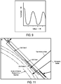
- FIG. 9 illustrates an example of a transmission versus voltage curve.
- the optical delta n of this LC is much larger than in an LC optimized for an LCD.
- the transmission versus voltage curve would look something like the plot in FIG. 9 .
- An optical transmission difference between the positive and negative frames are accentuated in parts of the optical transmission curve where the change in transmission with voltage is rapid (steep slope). Those regions should be used for determining correction voltages for gray levels.
- optical states for the positive and negative frames on the electro-optic curve will be different due to the DC offset. This difference between optical transmission values will be observed as a “flicker”.
- these optical states for the positive and negative frames on the electro-optic curve are used to correct the DC offset.
- the DC offset correction techniques disclosed herein generate a DC offset correction voltage that can be determined by nulling the “flicker”.
- the net DC offset is adjusted by adjusting the Vcom voltage. This may be for different driving modes. For example, in one embodiment, at a gross level, for a 1 ⁇ 2 VDD mode of driving (in which the voltage range between the positive and negative frames is 1 ⁇ 2 VDD), the net DC offset is adjusted by adjusting the Vcom voltage.
- the DC offset correction is performed by DC offset correction logic. In one embodiment, such logic comprises circuitry executing software and is coupled to circuitry such as shown in FIG. 4 to adjust the Vcom voltage. Alternatively, DC offset correction logic comprises hardware, software, firmware or a combination of two or more of these.
- the frame rate (lengthen the frame time) to increase the time the LC has to respond to the voltages of the positive and negative frames. This is because LC has a response time and one needs to wait for that response time to observe the optical response to voltage change. If the frame time isn't long enough to observe the LC response, the frame time used during DC offset calibration can be increased. However, the frame rate cannot be simply lengthened because the length of the frame time may affect key components of the DC offset, such as, for example, the charging ratio and voltage leakage.
- increasing the time the LC has to respond to the voltages of the positive and negative frames is accomplished by a drive mode where the frame times are kept at the same length, but multiple frames of positive voltage are written in a row, followed by an equal number of negative frames, and so on, until the null measurement is completed.
- the DC offset calibration is performed with that increased frame time but the initial frame time is still used for the antenna operation.
- FIG. 10 is a flow diagram of a one embodiment of a process to determine DC offset correction values.
- the process is performed by processing logic that may comprise hardware, software, firmware, or a combination of the three.
- operations set forth in FIG. 8 are performed by DC offset correction logic or a DC offset correction unit.
- the DC offset correction unit or logic is in a testing and calibration equipment used in the production line of an antenna.
- the process of FIG. 10 relies on observations related to the difference in optical transmission between the positive and negative frames.
- the optical transmission in the positive and negative frames is captured using optical structures.
- these optical structures are also used to test functionality of matrix row and column drivers for RF radiating antenna elements (e.g., surface scattering metamaterial antenna elements, such as, for example, described below).
- the process for obtaining correction values begins by processing logic driving the TFT/window test element at a gray level (processing block 1001 ) and observing the difference in optical transmission between the positive and negative frames (processing block 1002 ).
- Processing logic then nulls the flicker between frames by adjusting Vcom (processing block 1003 ).
- processing logic After adjusting Vcom to a level that nulls the flicker, processing logic converts the Vcom value to adjusted positive frame voltage Vpos and negative frame voltage Vneg (processing block 1004 ).
- processing logic applies the adjusted voltage to positive and negative frames (processing block 1005 ) and checks for flicker (processing block 1006 ).
- processing logic stores adjusted positive and negative frame voltages in correction look up table (processing block 1007 ).
- the process transitions back to processing block 1003 and the process repeats.
- processing logic moves to the next gray level and the process repeats (processing block 1008 ).
- the process is performed to null flicker for one element and after the process is completed for that element, the process moves to the next element and repeats until all the elements are tested.
- the corrections determined for RF TFT elements that were measured are used to determine corrections of unmeasured RF TFT elements.
- the DC offset correction unit interpolates the corrections for measured TFT/window test elements to unmeasured RF TFT elements. These unmeasured RF TFT elements may be located between the tested RF TFT elements and/or near the tested RF TFT elements.
- optically transparent test structures are used to observe flicker and determine the DC offset to null the flicker.
- these structures are located outside of the RF TFT element array and contain equivalent circuits the same or very similar as those found in the RF TFT aperture array in the aperture segment.
- Antenna segments are combined to form the entire antenna array.
- the optical characteristics of such structures are used to estimate and create correction values to reduce the DC offset in RF element array.
- the Gate 0 and Source 0 lines associated with voltages for the test structure are added outside of the waveguide region (e.g., a waveguide of FIG. 23 of the aperture where additional holes in the waveguide do not impact performance.
- FIG. 11 illustrates one embodiment of routing for a single test structure located outside of the waveguide area. Referring to FIG. 11 , Gate 0 , Source 0 and Vcom routing for voltages for the test structure are shown outside of the area the waveguide.
- FIG. 12 illustrates one embodiment of a test structure.
- the equivalent circuit of the test structure is designed to have the equivalent circuit of an RF element in the array.
- the capacitance of the device at the drain is sized to match the capacitance of the overlap of a patch element with the iris element.
- an optically transparent conductor layer such as, but not limited to, indium-tin-oxide (ITO), is used as an electrode on both sides of that capacitor. Observation windows are created in metal layers for optical response of the LC.
- ITO indium-tin-oxide
- TFT box 1252 includes a TFT and storage cap, such as, for example, but not limited to, FIG. 4 .
- Gate metal 1251 is for the gate voltage of the TFT
- source 1254 is for the source voltage of the TFT
- drain 1255 is for the drain voltage of the TFT that is coupled to a test antenna element (e.g., a surface scattering metamaterial antenna element).
- the gate and source are coupled to Gate 0 and Source 0 of FIG. 11 .
- the routing 1253 for Vcom is also shown coupled to the TFT 1252 .
- a hole 1258 in the iris metal is used as a window to view flicker using ITO 1256 on the iris (slot) substrate and ITO 1257 on the patch substrate, such as the patch and iris substrates described in more detail below.
- Gate 0 and Source 0 lines for the test structure are also added outside the waveguide region of the aperture.
- Gate 0 lines cross all of the source lines as the source lines cross from the source driver outside of the aperture segment to the inside of the segment (e.g., inside being the inside the border seal where the LC resides.)
- the Gate 0 can be extended to cross all of the Source lines, and the Source 0 can be extended to cross all of the Gate lines.
- Optically transparent test structures can be created where Gate 0 crosses the source lines and Source 0 crosses the gate lines
- FIG. 13 illustrates one example of gate and source line routing for optically transparent test structures.
- the routing is moved as far as possible outside of the waveguide region and spaces created in the fan out for TFT/window test elements.
- a TFT/window test structure similar to the one shown in FIG. 12 is placed at each source/Gate 0 junction, where the source could be Source 0 , Source 1 , . . . Source N (source of the last test transistor).
- gate driver 1301 provides the gate voltages for Gates 0 -N and source driver 1302 provides the source voltage for Sources 0 -N, where N designates the last of the gates and sources, respectively.
- gate driver 1301 and source driver 1302 are at the edge of the antenna aperture segment.
- FIGS. 14 and 15 illustrate examples of patch glass (substrate) and iris glass (substrate) structures, respectively, that form the patch and iris for the antenna aperture.
- An example of the glass and iris substrates are described in greater detail below.
- patch glass substrate 1470 for an antenna aperture segment includes antenna element aperture boundary 1471 that represents the boundary of the antenna element array (with antenna elements to the left of boundary 1471 ).
- antenna element aperture boundary 1471 that represents the boundary of the antenna element array (with antenna elements to the left of boundary 1471 ).
- optically transparent test structures e.g., ITO holes, or windows
- TFTs and storage capacitor
- FIG. 15 illustrates iris glass substrate 1501 with a ring of holes 1502 in the iris metal layer corresponding to the ITO drains on the patch glass substrate.
- ITO pads 1503 over openings in the iris metal layer correspond to the ITO on the patch glass substrate ITO is connected to Vcom.
- the DC offset in the RF element waveform is optically nulled in these structures and the resulting “null” values are used to set Vcom and correct the DC offset in RF elements in the array.
- these structures are also used to test the functionality of the source and gate drivers at the beginning of the array via an optical mechanism.
- a Source 0 is routed to cross the gate lines as they enter the segment.
- the gate routing is moved and spaces are created to place a TFT/window test element at each Gate/Source 0 junction.
- FIGS. 16 and 17 illustrate examples of this routing on the patch glass substrate and iris glass substrate, respectively.
- patch glass substrate 1601 includes an antenna element aperture 1602 with an antenna aperture boundary 1603 .
- Test structures 1604 with their TFT (with storage capacitor) and their ITO hole (window) are coupled to gate driver 1605 and source driver 1606 .
- Gate and Vcom routing continue from test structures 1604 into antenna element aperture 1602 .
- iris glass substrate 1701 is shown with a ring of windows (openings) 1703 in the iris metal layer (corresponding to ITO drains on the patch glass substrate) with ITO pads 1704 over the iris metal openings. Pads 1704 are connected to Vcom.
- the DC offset in the RF element waveform is optically nulled in these structures and the resulting “null” values used to set Vcom and correct the DC offset in RF elements in the array.
- these structures are also used to test the functionality of the source and gate drivers at the beginning of the array by an optical mechanism.
- the optically transparent test structures are not limited to being outside the antenna element array.
- the TFT/optical window test element replaces some RF TFT elements in the antenna array. Due to the holographic nature of forming a beam, an aperture with some small number of elements missing can form beams with a negligible decrease in performance compared to antennas with fully functioning RF element arrays.
- RF elements in certain locations are replaced with TFT/window test elements.
- the voltage values used to optically null these the TFT/window test elements are used to create a mapping of corrections, which is used to interpolate correction values for the RF element array. In one embodiment, this mapping is stored in a look up table.
- these TFT/window test elements are not placed in the RF element array according to their geometric position, but are placed according to their position as an equivalent circuit of the array.
- the “first” and “last” elements for example, in frame inversion, the first scanned and last scanned, will not have the same bias over the TFT for the same lengths of time.
- the RC time constant to the TFT is not the same, etc.
- Some places may be more highly contaminated (fill opening). Therefore, the DC offset may be different in these places.
- the placement location is the location from an electronic point of view and not a geometric point of view. This might mean an element of the first source and first gate line, an element of the first source and the last gate lines, an element of the last source and first gate, an element of the last source and last gate, etc.
- the techniques described herein are not limited to such a mode.
- the LC optical response is observed using a reflective LC mode instead of a transmissive LC mode.
- the RF ripple correction, DC offset correction and voltage adjustment techniques described above may be used in a number of antenna embodiments, including, but not limited to, flat panel antennas.
- Embodiments of such flat panel antennas are disclosed.
- the flat panel antennas include one or more arrays of antenna elements on an antenna aperture.
- the antenna elements comprise liquid crystal cells.
- the flat panel antenna is a cylindrically fed antenna that includes matrix drive circuitry to uniquely address and drive each of the antenna elements that are not placed in rows and columns. In one embodiment, the elements are placed in rings.
- the antenna aperture having the one or more arrays of antenna elements is comprised of multiple segments coupled together. When coupled together, the combination of the segments form closed concentric rings of antenna elements. In one embodiment, the concentric rings are concentric with respect to the antenna feed.
- the flat panel antenna is part of a metamaterial antenna system.
- a metamaterial antenna system for communications satellite earth stations are described.
- the antenna system is a component or subsystem of a satellite earth station (ES) operating on a mobile platform (e.g., aeronautical, maritime, land, etc.) that operates using either Ka-band frequencies or Ku-band frequencies for civil commercial satellite communications.
- ES satellite earth station
- mobile platform e.g., aeronautical, maritime, land, etc.
- embodiments of the antenna system also can be used in earth stations that are not on mobile platforms (e.g., fixed or transportable earth stations).
- the antenna system uses surface scattering metamaterial technology to form and steer transmit and receive beams through separate antennas.
- the antenna systems are analog systems, in contrast to antenna systems that employ digital signal processing to electrically form and steer beams (such as phased array antennas).
- the antenna system is comprised of three functional subsystems: (1) a wave guiding structure consisting of a cylindrical wave feed architecture; (2) an array of wave scattering metamaterial unit cells that are part of antenna elements; and (3) a control structure to command formation of an adjustable radiation field (beam) from the metamaterial scattering elements using holographic principles.
- a wave guiding structure consisting of a cylindrical wave feed architecture
- an array of wave scattering metamaterial unit cells that are part of antenna elements
- a control structure to command formation of an adjustable radiation field (beam) from the metamaterial scattering elements using holographic principles.
- FIG. 18 illustrates the schematic of one embodiment of a cylindrically fed holographic radial aperture antenna.
- the antenna aperture has one or more arrays 654 of antenna elements 653 that are placed in concentric rings around an input feed 652 of the cylindrically fed antenna.
- antenna elements 653 are radio frequency (RF) resonators that radiate RF energy.
- antenna elements 653 comprise both Rx and Tx irises that are interleaved and distributed on the whole surface of the antenna aperture. Examples of such antenna elements are described in greater detail below. Note that the RF resonators described herein may be used in antennas that do not include a cylindrical feed.
- the antenna includes a coaxial feed that is used to provide a cylindrical wave feed via input feed 652 .
- the cylindrical wave feed architecture feeds the antenna from a central point with an excitation that spreads outward in a cylindrical manner from the feed point. That is, a cylindrically fed antenna creates an outward travelling concentric feed wave. Even so, the shape of the cylindrical feed antenna around the cylindrical feed can be circular, square or any shape. In another embodiment, a cylindrically fed antenna creates an inward travelling feed wave. In such a case, the feed wave most naturally comes from a circular structure.
- antenna elements 653 comprise irises and the aperture antenna of FIG. 18 is used to generate a main beam shaped by using excitation from a cylindrical feed wave for radiating irises through tunable liquid crystal (LC) material.
- the antenna can be excited to radiate a horizontally or vertically polarized electric field at desired scan angles.
- the antenna elements comprise a group of patch antennas.
- This group of patch antennas comprises an array of scattering metamaterial elements.
- each scattering element in the antenna system is part of a unit cell that consists of a lower conductor, a dielectric substrate and an upper conductor that embeds a complementary electric inductive-capacitive resonator (“complementary electric LC” or “CELC”) that is etched in or deposited onto the upper conductor.
- CELC complementary electric inductive-capacitive resonator
- LC in the context of CELC refers to inductance-capacitance, as opposed to liquid crystal.
- a liquid crystal is disposed in the gap around the scattering element. This LC is driven by the direct drive embodiments described above.
- liquid crystal is encapsulated in each unit cell and separates the lower conductor associated with a slot from an upper conductor associated with its patch.
- Liquid crystal has a permittivity that is a function of the orientation of the molecules comprising the liquid crystal, and the orientation of the molecules (and thus the permittivity) can be controlled by adjusting the bias voltage across the liquid crystal.
- the liquid crystal integrates an on/off switch for the transmission of energy from the guided wave to the CELC. When switched on, the CELC emits an electromagnetic wave like an electrically small dipole antenna. Note that the teachings herein are not limited to having a liquid crystal that operates in a binary fashion with respect to energy transmission.
- the feed geometry of this antenna system allows the antenna elements to be positioned at forty-five-degree (45°) angles to the vector of the wave in the wave feed. Note that other positions may be used (e.g., at 40° angles). This position of the elements enables control of the free space wave received by or transmitted/radiated from the elements.
- the antenna elements are arranged with an inter-element spacing that is less than a free-space wavelength of the operating frequency of the antenna. For example, if there are four scattering elements per wavelength, the elements in the 30 GHz transmit antenna will be approximately 2.5 mm (i.e., 1 ⁇ 4th the 10 mm free-space wavelength of 30 GHz).
- the two sets of elements are perpendicular to each other and simultaneously have equal amplitude excitation if controlled to the same tuning state. Rotating them +/ ⁇ 45 degrees relative to the feed wave excitation achieves both desired features at once. Rotating one set 0 degrees and the other 90 degrees would achieve the perpendicular goal, but not the equal amplitude excitation goal. Note that 0 and 90 degrees may be used to achieve isolation when feeding the array of antenna elements in a single structure from two sides.
- the amount of radiated power from each unit cell is controlled by applying a voltage to the patch (potential across the LC channel) using a controller. Traces to each patch are used to provide the voltage to the patch antenna. The voltage is used to tune or detune the capacitance and thus the resonance frequency of individual elements to effectuate beam forming. The voltage required is dependent on the liquid crystal mixture being used.
- the voltage tuning characteristic of liquid crystal mixtures is mainly described by a threshold voltage at which the liquid crystal starts to be affected by the voltage and the saturation voltage, above which an increase of the voltage does not cause major tuning in liquid crystal. These two characteristic parameters can change for different liquid crystal mixtures.
- a matrix drive is used to apply voltage to the patches in order to drive each cell separately from all the other cells without having a separate connection for each cell (direct drive). Because of the high density of elements, the matrix drive is an efficient way to address each cell individually.
- the control structure for the antenna system has 2 main components: the antenna array controller, which includes drive electronics, for the antenna system, is below the wave scattering structure, while the matrix drive switching array is interspersed throughout the radiating RF array in such a way as to not interfere with the radiation.
- the drive electronics for the antenna system comprise commercial off-the shelf LCD controls used in commercial television appliances that adjust the bias voltage for each scattering element by adjusting the amplitude or duty cycle of an AC bias signal to that element.
- the antenna array controller also contains a microprocessor executing the software.
- the control structure may also incorporate sensors (e.g., a GPS receiver, a three-axis compass, a 3-axis accelerometer, 3-axis gyro, 3-axis magnetometer, etc.) to provide location and orientation information to the processor.
- sensors e.g., a GPS receiver, a three-axis compass, a 3-axis accelerometer, 3-axis gyro, 3-axis magnetometer, etc.
- the location and orientation information may be provided to the processor by other systems in the earth station and/or may not be part of the antenna system.
- the antenna array controller controls which elements are turned off and those elements turned on and at which phase and amplitude level at the frequency of operation.
- the elements are selectively detuned for frequency operation by voltage application.
- a controller supplies an array of voltage signals to the RF patches to create a modulation, or control pattern.
- the control pattern causes the elements to be turned to different states.
- multistate control is used in which various elements are turned on and off to varying levels, further approximating a sinusoidal control pattern, as opposed to a square wave (i.e., a sinusoid gray shade modulation pattern).
- some elements radiate more strongly than others, rather than some elements radiate and some do not.
- Variable radiation is achieved by applying specific voltage levels, which adjusts the liquid crystal permittivity to varying amounts, thereby detuning elements variably and causing some elements to radiate more than others.
- the generation of a focused beam by the metamaterial array of elements can be explained by the phenomenon of constructive and destructive interference.
- Individual electromagnetic waves sum up (constructive interference) if they have the same phase when they meet in free space and waves cancel each other (destructive interference) if they are in opposite phase when they meet in free space.
- the slots in a slotted antenna are positioned so that each successive slot is positioned at a different distance from the excitation point of the guided wave, the scattered wave from that element will have a different phase than the scattered wave of the previous slot. If the slots are spaced one quarter of a guided wavelength apart, each slot will scatter a wave with a one fourth phase delay from the previous slot.
- the number of patterns of constructive and destructive interference that can be produced can be increased so that beams can be pointed theoretically in any direction plus or minus ninety degrees (90°) from the bore sight of the antenna array, using the principles of holography.
- the antenna can change the direction of the main beam.
- the time required to turn the unit cells on and off dictates the speed at which the beam can be switched from one location to another location.
- the antenna system produces one steerable beam for the uplink antenna and one steerable beam for the downlink antenna.
- the antenna system uses metamaterial technology to receive beams and to decode signals from the satellite and to form transmit beams that are directed toward the satellite.
- the antenna systems are analog systems, in contrast to antenna systems that employ digital signal processing to electrically form and steer beams (such as phased array antennas).
- the antenna system is considered a “surface” antenna that is planar and relatively low profile, especially when compared to conventional satellite dish receivers.
- FIG. 19 illustrates a perspective view of one row of antenna elements that includes a ground plane and a reconfigurable resonator layer.
- Reconfigurable resonator layer 1230 includes an array of tunable slots 1210 .
- the array of tunable slots 1210 can be configured to point the antenna in a desired direction.
- Each of the tunable slots can be tuned/adjusted by varying a voltage across the liquid crystal.
- Control module 1280 is coupled to reconfigurable resonator layer 1230 to modulate the array of tunable slots 1210 by varying the voltage across the liquid crystal in FIG. 20 .
- Control module 1280 may include a Field Programmable Gate Array (“FPGA”), a microprocessor, a controller, System-on-a-Chip (SoC), or other processing logic.
- control module 1280 includes logic circuitry (e.g., multiplexer) to drive the array of tunable slots 1210 .
- control module 1280 receives data that includes specifications for a holographic diffraction pattern to be driven onto the array of tunable slots 1210 .
- the holographic diffraction patterns may be generated in response to a spatial relationship between the antenna and a satellite so that the holographic diffraction pattern steers the downlink beams (and uplink beam if the antenna system performs transmit) in the appropriate direction for communication.
- a control module similar to control module 1280 may drive each array of tunable slots described in the figures of the disclosure.
- Radio Frequency (“RF”) holography is also possible using analogous techniques where a desired RF beam can be generated when an RF reference beam encounters an RF holographic diffraction pattern.
- the reference beam is in the form of a feed wave, such as feed wave 1205 (approximately 20 GHz in some embodiments).
- feed wave 1205 approximately 20 GHz in some embodiments.
- an interference pattern is calculated between the desired RF beam (the object beam) and the feed wave (the reference beam).
- the interference pattern is driven onto the array of tunable slots 1210 as a diffraction pattern so that the feed wave is “steered” into the desired RF beam (having the desired shape and direction).
- the feed wave encountering the holographic diffraction pattern “reconstructs” the object beam, which is formed according to design requirements of the communication system.
- FIG. 20 illustrates one embodiment of a tunable resonator/slot 1210 .
- Tunable slot 1210 includes an iris/slot 1212 , a radiating patch 1211 , and liquid crystal 1213 disposed between iris 1212 and patch 1211 .
- radiating patch 1211 is co-located with iris 1212 .
- FIG. 21 illustrates a cross section view of one embodiment of a physical antenna aperture.
- the antenna aperture includes ground plane 1245 , and a metal layer 1236 within iris layer 1233 , which is included in reconfigurable resonator layer 1230 .
- the antenna aperture of FIG. 21 includes a plurality of tunable resonator/slots 1210 of FIG. 20 .
- Iris/slot 1212 is defined by openings in metal layer 1236 .
- a feed wave, such as feed wave 1205 of FIG. 20 may have a microwave frequency compatible with satellite communication channels. The feed wave propagates between ground plane 1245 and resonator layer 1230 .
- Reconfigurable resonator layer 1230 also includes gasket layer 1232 and patch layer 1231 .
- Gasket layer 1232 is disposed between patch layer 1231 and iris layer 1233 .
- a spacer could replace gasket layer 1232 .
- iris layer 1233 is a printed circuit board (“PCB”) that includes a copper layer as metal layer 1236 .
- PCB printed circuit board
- iris layer 1233 is glass. Iris layer 1233 may be other types of substrates.
- Openings may be etched in the copper layer to form slots 1212 .
- iris layer 1233 is conductively coupled by a conductive bonding layer to another structure (e.g., a waveguide) in FIG. 21 . Note that in an embodiment the iris layer is not conductively coupled by a conductive bonding layer and is instead interfaced with a non-conducting bonding layer.
- Patch layer 1231 may also be a PCB that includes metal as radiating patches 1211 .
- gasket layer 1232 includes spacers 1239 that provide a mechanical standoff to define the dimension between metal layer 1236 and patch 1211 .
- the spacers are 75 microns, but other sizes may be used (e.g., 3-200 mm).
- the antenna aperture of FIG. 21 includes multiple tunable resonator/slots, such as tunable resonator/slot 1210 includes patch 1211 , liquid crystal 1213 , and iris 1212 of FIG. 20 .
- the chamber for liquid crystal 1213 is defined by spacers 1239 , iris layer 1233 and metal layer 1236 . When the chamber is filled with liquid crystal, patch layer 1231 can be laminated onto spacers 1239 to seal liquid crystal within resonator layer 1230 .
- a voltage between patch layer 1231 and iris layer 1233 can be modulated to tune the liquid crystal in the gap between the patch and the slots (e.g., tunable resonator/slot 1210 ). Adjusting the voltage across liquid crystal 1213 varies the capacitance of a slot (e.g., tunable resonator/slot 1210 ). Accordingly, the reactance of a slot (e.g., tunable resonator/slot 1210 ) can be varied by changing the capacitance. The resonant frequency of slot 1210 also changes according to the equation
- f 1 2 ⁇ ⁇ ⁇ LC , where f is the resonant frequency of slot 1210 and L and C are the inductance and capacitance of slot 1210 , respectively.
- the resonant frequency of slot 1210 affects the energy radiated from feed wave 1205 propagating through the waveguide. As an example, if feed wave 1205 is 20 GHz, the resonant frequency of a slot 1210 may be adjusted (by varying the capacitance) to 17 GHz so that the slot 1210 couples substantially no energy from feed wave 1205 . Or, the resonant frequency of a slot 1210 may be adjusted to 20 GHz so that the slot 1210 couples energy from feed wave 1205 and radiates that energy into free space.
- tunable slots in a row are spaced from each other by ⁇ /5. Other spacings may be used. In one embodiment, each tunable slot in a row is spaced from the closest tunable slot in an adjacent row by ⁇ /2, and, thus, commonly oriented tunable slots in different rows are spaced by ⁇ /4, though other spacings are possible (e.g., ⁇ /5, ⁇ /6.3). In another embodiment, each tunable slot in a row is spaced from the closest tunable slot in an adjacent row by ⁇ /3.
- Embodiments use reconfigurable metamaterial technology, such as described in U.S. patent application Ser. No. 14/550,178, entitled “Dynamic Polarization and Coupling Control from a Steerable Cylindrically Fed Holographic Antenna”, filed Nov. 21, 2014 and U.S. patent application Ser. No. 14/610,502, entitled “Ridged Waveguide Feed Structures for Reconfigurable Antenna”, filed Jan. 30, 2015.
- FIGS. 22A-D illustrate one embodiment of the different layers for creating the slotted array.
- the antenna array includes antenna elements that are positioned in rings, such as the example rings shown in FIG. 18 . Note that in this example the antenna array has two different types of antenna elements that are used for two different types of frequency bands.
- FIG. 22A illustrates a portion of the first iris board layer with locations corresponding to the slots.
- the circles are open areas/slots in the metallization in the bottom side of the iris substrate, and are for controlling the coupling of elements to the feed (the feed wave). Note that this layer is an optional layer and is not used in all designs.
- FIG. 22B illustrates a portion of the second iris board layer containing slots.
- FIG. 22C illustrates patches over a portion of the second iris board layer.
- FIG. 22D illustrates a top view of a portion of the slotted array.
- FIG. 23 illustrates a side view of one embodiment of a cylindrically fed antenna structure.
- the antenna produces an inwardly travelling wave using a double layer feed structure (i.e., two layers of a feed structure).
- the antenna includes a circular outer shape, though this is not required. That is, non-circular inward travelling structures can be used.
- the antenna structure in FIG. 23 includes a coaxial feed, such as, for example, described in U.S. Publication No. 2015/0236412, entitled “Dynamic Polarization and Coupling Control from a Steerable Cylindrically Fed Holographic Antenna”, filed on Nov. 21, 2014.
- a coaxial pin 1601 is used to excite the field on the lower level of the antenna.
- coaxial pin 1601 is a 50 ⁇ coax pin that is readily available.
- Coaxial pin 1601 is coupled (e.g., bolted) to the bottom of the antenna structure, which is conducting ground plane 1602 .
- interstitial conductor 1603 Separate from conducting ground plane 1602 is interstitial conductor 1603 , which is an internal conductor.
- conducting ground plane 1602 and interstitial conductor 1603 are parallel to each other.
- the distance between ground plane 1602 and interstitial conductor 1603 is 0.1-0.15′′. In another embodiment, this distance may be ⁇ /2, where ⁇ is the wavelength of the travelling wave at the frequency of operation.
- Ground plane 1602 is separated from interstitial conductor 1603 via a spacer 1604 .
- spacer 1604 is a foam or air-like spacer.
- spacer 1604 comprises a plastic spacer.
- dielectric layer 1605 On top of interstitial conductor 1603 is dielectric layer 1605 .
- dielectric layer 1605 is plastic.
- the purpose of dielectric layer 1605 is to slow the travelling wave relative to free space velocity. In one embodiment, dielectric layer 1605 slows the travelling wave by 30% relative to free space.
- the range of indices of refraction that are suitable for beam forming are 1.2-1.8, where free space has by definition an index of refraction equal to 1.
- Other dielectric spacer materials such as, for example, plastic, may be used to achieve this effect. Note that materials other than plastic may be used as long as they achieve the desired wave slowing effect.
- a material with distributed structures may be used as dielectric 1605 , such as periodic sub-wavelength metallic structures that can be machined or lithographically defined, for example.
- An RF-array 1606 is on top of dielectric 1605 .
- the distance between interstitial conductor 1603 and RF-array 1606 is 0.1-0.15′′. In another embodiment, this distance may be ⁇ eff /2, where ⁇ eff is the effective wavelength in the medium at the design frequency.
- the antenna includes sides 1607 and 1608 .
- Sides 1607 and 1608 are angled to cause a travelling wave feed from coax pin 1601 to be propagated from the area below interstitial conductor 1603 (the spacer layer) to the area above interstitial conductor 1603 (the dielectric layer) via reflection.
- the angle of sides 1607 and 1608 are at 45° angles.
- sides 1607 and 1608 could be replaced with a continuous radius to achieve the reflection. While FIG. 23 shows angled sides that have angle of 45 degrees, other angles that accomplish signal transmission from lower level feed to upper level feed may be used.
- the 45° angles are replaced with a single step.
- the steps on one end of the antenna go around the dielectric layer, interstitial the conductor, and the spacer layer. The same two steps are at the other ends of these layers.
- the wave In operation, when a feed wave is fed in from coaxial pin 1601 , the wave travels outward concentrically oriented from coaxial pin 1601 in the area between ground plane 1602 and interstitial conductor 1603 .
- the concentrically outgoing waves are reflected by sides 1607 and 1608 and travel inwardly in the area between interstitial conductor 1603 and RF array 1606 .
- the reflection from the edge of the circular perimeter causes the wave to remain in phase (i.e., it is an in-phase reflection).
- the travelling wave is slowed by dielectric layer 1605 . At this point, the travelling wave starts interacting and exciting with elements in RF array 1606 to obtain the desired scattering.
- a termination 1609 is included in the antenna at the geometric center of the antenna.
- termination 1609 comprises a pin termination (e.g., a 50 ⁇ pin).
- termination 1609 comprises an RF absorber that terminates unused energy to prevent reflections of that unused energy back through the feed structure of the antenna. These could be used at the top of RF array 1606 .
- FIG. 24 illustrates another embodiment of the antenna system with an outgoing wave.
- two ground planes 1610 and 1611 are substantially parallel to each other with a dielectric layer 1612 (e.g., a plastic layer, etc.) in between ground planes.
- RF absorbers 1619 e.g., resistors
- a coaxial pin 1615 e.g., 50 ⁇ feeds the antenna.
- An RF array 1616 is on top of dielectric layer 1612 and ground plane 1611 .
- a feed wave is fed through coaxial pin 1615 and travels concentrically outward and interacts with the elements of RF array 1616 .
- the cylindrical feed in both the antennas of FIGS. 23 and 24 improves the service angle of the antenna.
- the antenna system has a service angle of seventy-five degrees (75°) from the bore sight in all directions.
- the overall antenna gain is dependent on the gain of the constituent elements, which themselves are angle-dependent.
- the overall antenna gain typically decreases as the beam is pointed further off bore sight. At 75 degrees off bore sight, significant gain degradation of about 6 dB is expected.
- Embodiments of the antenna having a cylindrical feed solve one or more problems. These include dramatically simplifying the feed structure compared to antennas fed with a corporate divider network and therefore reducing total required antenna and antenna feed volume; decreasing sensitivity to manufacturing and control errors by maintaining high beam performance with coarser controls (extending all the way to simple binary control); giving a more advantageous side lobe pattern compared to rectilinear feeds because the cylindrically oriented feed waves result in spatially diverse side lobes in the far field; and allowing polarization to be dynamic, including allowing left-hand circular, right-hand circular, and linear polarizations, while not requiring a polarizer.
- RF array 1606 of FIG. 23 and RF array 1616 of FIG. 24 include a wave scattering subsystem that includes a group of patch antennas (e.g., surface scatterers) that act as radiators.
- This group of patch antennas comprises an array of scattering metamaterial elements.
- each scattering element in the antenna system is part of a unit cell that consists of a lower conductor, a dielectric substrate and an upper conductor that embeds a complementary electric inductive-capacitive resonator (“complementary electric LC” or “CELL”) that is etched in or deposited onto the upper conductor.
- a complementary electric inductive-capacitive resonator (“complementary electric LC” or “CELL”) that is etched in or deposited onto the upper conductor.
- a liquid crystal is injected in the gap around the scattering element.
- Liquid crystal is encapsulated in each unit cell and separates the lower conductor associated with a slot from an upper conductor associated with its patch.
- Liquid crystal has a permittivity that is a function of the orientation of the molecules comprising the liquid crystal, and the orientation of the molecules (and thus the permittivity) can be controlled by adjusting the bias voltage across the liquid crystal. Using this property, the liquid crystal acts as an on/off switch for the transmission of energy from the guided wave to the CELC. When switched on, the CELC emits an electromagnetic wave like an electrically small dipole antenna.
- Controlling the thickness of the LC increases the beam switching speed.
- a fifty percent (50%) reduction in the gap between the lower and the upper conductor results in a fourfold increase in speed.
- the thickness of the liquid crystal results in a beam switching speed of approximately fourteen milliseconds (14 ms).
- the LC is doped in a manner well-known in the art to improve responsiveness so that a seven millisecond (7 ms) requirement can be met.
- the CELC element is responsive to a magnetic field that is applied parallel to the plane of the CELC element and perpendicular to the CELC gap complement.
- a voltage is applied to the liquid crystal in the metamaterial scattering unit cell, the magnetic field component of the guided wave induces a magnetic excitation of the CELC, which, in turn, produces an electromagnetic wave in the same frequency as the guided wave.
- the phase of the electromagnetic wave generated by a single CELC can be selected by the position of the CELC on the vector of the guided wave.
- Each cell generates a wave in phase with the guided wave parallel to the CELC. Because the CELCs are smaller than the wave length, the output wave has the same phase as the phase of the guided wave as it passes beneath the CELC.
- the cylindrical feed geometry of this antenna system allows the CELC elements to be positioned at forty-five-degree (45°) angles to the vector of the wave in the wave feed. This position of the elements enables control of the polarization of the free space wave generated from or received by the elements.
- the CELCs are arranged with an inter-element spacing that is less than a free-space wavelength of the operating frequency of the antenna. For example, if there are four scattering elements per wavelength, the elements in the 30 GHz transmit antenna will be approximately 2.5 mm (i.e., 1 ⁇ 4th the 10 mm free-space wavelength of 30 GHz).
- the CELCs are implemented with patch antennas that include a patch co-located over a slot with liquid crystal between the two.
- the metamaterial antenna acts like a slotted (scattering) wave guide. With a slotted wave guide, the phase of the output wave depends on the location of the slot in relation to the guided wave.
- the antenna elements are placed on the cylindrical feed antenna aperture in a way that allows for a systematic matrix drive circuit.
- the placement of the cells includes placement of the transistors for the matrix drive.
- FIG. 25 illustrates one embodiment of the placement of matrix drive circuitry with respect to antenna elements.
- row controller 1701 is coupled to transistors 1711 and 1712 , via row select signals Row 1 and Row 2 , respectively, and column controller 1702 is coupled to transistors 1711 and 1712 via column select signal Column 1 .
- Transistor 1711 is also coupled to antenna element 1721 via connection to patch 1731
- transistor 1712 is coupled to antenna element 1722 via connection to patch 1732 .
- the cells are placed on concentric rings and each of the cells is connected to a transistor that is placed beside the cell and acts as a switch to drive each cell separately.
- the matrix drive circuitry is built in order to connect every transistor with a unique address as the matrix drive approach requires. Because the matrix drive circuit is built by row and column traces (similar to LCDs) but the cells are placed on rings, there is no systematic way to assign a unique address to each transistor. This mapping problem results in very complex circuitry to cover all the transistors and leads to a significant increase in the number of physical traces to accomplish the routing. Because of the high density of cells, those traces disturb the RF performance of the antenna due to coupling effect. Also, due to the complexity of traces and high packing density, the routing of the traces cannot be accomplished by commercially available layout tools.
- the matrix drive circuitry is predefined before the cells and transistors are placed. This ensures a minimum number of traces that are necessary to drive all the cells, each with a unique address. This strategy reduces the complexity of the drive circuitry and simplifies the routing, which subsequently improves the RF performance of the antenna.
- the cells are placed on a regular rectangular grid composed of rows and columns that describe the unique address of each cell.
- the cells are grouped and transformed to concentric circles while maintaining their address and connection to the rows and columns as defined in the first step.
- a goal of this transformation is not only to put the cells on rings but also to keep the distance between cells and the distance between rings constant over the entire aperture. In order to accomplish this goal, there are several ways to group the cells.
- a TFT package is used to enable placement and unique addressing in the matrix drive.
- FIG. 26 illustrates one embodiment of a TFT package. Referring to FIG. 26 , a TFT and a hold capacitor 1803 is shown with input and output ports. There are two input ports connected to traces 1801 and two output ports connected to traces 1802 to connect the TFTs together using the rows and columns. In one embodiment, the row and column traces cross in 90° angles to reduce, and potentially minimize, the coupling between the row and column traces. In one embodiment, the row and column traces are on different layers.
- FIG. 27 is a block diagram of an embodiment of a communication system having simultaneous transmit and receive paths. While only one transmit path and one receive path are shown, the communication system may include more than one transmit path and/or more than one receive path.
- antenna 1401 includes two spatially interleaved antenna arrays operable independently to transmit and receive simultaneously at different frequencies as described above.
- antenna 1401 is coupled to diplexer 1445 .
- the coupling may be by one or more feeding networks.
- diplexer 1445 combines the two signals and the connection between antenna 1401 and diplexer 1445 is a single broad-band feeding network that can carry both frequencies.
- Diplexer 1445 is coupled to a low noise block down converter (LNB) 1427 , which performs a noise filtering function and a down conversion and amplification function in a manner well-known in the art.
- LNB 1427 is in an out-door unit (ODU).
- ODU out-door unit
- LNB 1427 is integrated into the antenna apparatus.
- LNB 1427 is coupled to a modem 1460 , which is coupled to computing system 1440 (e.g., a computer system, modem, etc.).
- Modem 1460 includes an analog-to-digital converter (ADC) 1422 , which is coupled to LNB 1427 , to convert the received signal output from diplexer 1445 into digital format. Once converted to digital format, the signal is demodulated by demodulator 1423 and decoded by decoder 1424 to obtain the encoded data on the received wave. The decoded data is then sent to controller 1425 , which sends it to computing system 1440 .
- ADC analog-to-digital converter
- Modem 1460 also includes an encoder 1430 that encodes data to be transmitted from computing system 1440 .
- the encoded data is modulated by modulator 1431 and then converted to analog by digital-to-analog converter (DAC) 1432 .
- DAC digital-to-analog converter
- the analog signal is then filtered by a BUC (up-convert and high pass amplifier) 1433 and provided to one port of diplexer 1445 .
- BUC 1433 is in an out-door unit (ODU).
- Diplexer 1445 operating in a manner well-known in the art provides the transmit signal to antenna 1401 for transmission.
- Controller 1450 controls antenna 1401 , including the two arrays of antenna elements on the single combined physical aperture.
- the communication system would be modified to include the combiner/arbiter described above. In such a case, the combiner/arbiter after the modem but before the BUC and LNB.
- the full duplex communication system shown in FIG. 27 has a number of applications, including but not limited to, internet communication, vehicle communication (including software updating), etc.
- Example 1 is an antenna comprising: an array of antenna elements having liquid crystal (LC); drive circuitry coupled to the array and having a plurality of drivers, each driver of the plurality of drivers coupled to an antenna element of the array and operable to apply a drive voltage to the antenna element; and radio-frequency (RF) ripple correction logic coupled to the drive circuitry to adjust drive voltages to compensate for ripple.
- LC liquid crystal
- RF radio-frequency
- Example 2 is the antenna of example 1 that may optionally include that the RF ripple correction logic is operable to readjust driving voltages for antenna elements of the array to apply a same differential voltage in both a positive frame and a negative frame.
- Example 3 is the antenna of example 2 that may optionally include that each driver of the plurality of drivers has an output defined at each gray shade level, of a plurality of gray shade levels, for both negative and positive frames and a gamma voltage controls the output.
- Example 4 is the antenna of example 3 that may optionally include that the RF ripple correction logic is operable to perform RF ripple correction at N/2 gray shade levels for N gamma voltage levels, where N is an integer.
- Example 5 is the antenna of example 1 that may optionally include that a common voltage is applied to antenna elements in the array, and further wherein the RF ripple correction logic is operable to adjust the common voltage to compensate for ripple.
- Example 6 is the antenna of example 1 that may optionally include a controller coupled to the drive circuitry to invert polarity of a differential voltage applied on the LC of the antenna elements periodically.
- Example 7 is the antenna of example 6 that may optionally include that the controller is operable to cause the drive circuitry to invert polarity of a differential voltage applied on the LC of antenna elements every frame.
- Example 8 is the antenna of example 1 that may optionally include that the RF ripple correction logic is operable to apply voltage adjustments as applied in a free space test (FST) measurement system.
- FST free space test
- Example 9 is the antenna of example 1 that may optionally include that the RF ripple correction logic is operable to apply voltage adjustments in response to environmental sensors coupled to the array.
- Example 10 is a method comprising: determining an initial set of driving voltages for drivers for antenna elements in an array of antenna elements in an antenna; and performing RF ripple correction for antenna elements in the array by adjusting driving voltages in the set of driving voltages.
- Example 11 is the method of example 10 that may optionally include applying RF ripple corrected voltages to the antenna elements in the array during operation.
- Example 12 is the method of example 11 that may optionally include that voltages in the initial set of voltages are symmetric with respect to an initial value for a common voltage.
- Example 13 is the method of example 12 that may optionally include that performing RF ripple correction for antenna elements in the array comprises: (a) measuring RF ripple using a first voltage level; (b) adjusting the common voltage based on a relationship between measured RF ripple and predetermined criteria; (c) repeating (a) and (b) until measured RF ripple satisfies the predetermined criteria; and (d) setting the common voltage to the adjusted common voltage.
- Example 14 is the method of example 13 that may optionally include that the first voltage level is based on a highest and lowest gray shade levels.
- Example 15 is the method of example 13 that may optionally include that the predetermined criteria are an RF ripple threshold and further wherein adjusting the common voltage is repeated until the RF ripple is below the threshold.
- Example 16 is the method of example 13 that may optionally include repeating adjustments to the common voltage for other gray shade levels.
- Example 17 is the method of example 10 that may optionally include that the drive voltages are the differential voltages across liquid crystal (LC) in the antenna elements.
- the drive voltages are the differential voltages across liquid crystal (LC) in the antenna elements.
- Example 18 is the method of example 10 that may optionally include producing adjusted drive voltages by: determining a differential of the common voltage; calculating source voltage corrections based on the differential; and applying the source voltage corrections by adjusting one or more gamma voltage levels.
- Example 19 is a non-transitory computer readable storage media having instructions stored thereupon which, when executed by a system having at least a processor and a memory therein, cause the system to perform a method comprising: determining an initial set of driving voltages for drivers for antenna elements in an array of antenna elements in an antenna; and performing RF ripple correction for antenna elements in the array by adjusting driving voltages in the set of driving voltages.
- Example 20 is the computer readable storage media of example 19 that may optionally include applying RF ripple corrected voltages to the antenna elements in the array during operation.
- Example 21 is the computer readable storage media of example 19 that may optionally include that voltages in the initial set of voltages are symmetric with respect to an initial value for a common voltage.
- Example 22 is the computer readable storage media of example 19 that may optionally include that performing RF ripple correction for antenna elements in the array comprises: (a) measuring RF ripple using a first voltage level; (b) adjusting the common voltage based on a relationship between measured RF ripple and predetermined criteria; (c) repeating (a) and (b) until measured RF ripple satisfies the predetermined criteria; and (d) setting the common voltage to the adjusted common voltage.
- Example 23 is the computer readable storage media of example 22 that may optionally include that the first voltage level is based on a highest and lowest gray shade levels.
- Example 24 is the computer readable storage media of example 22 that may optionally include that the predetermined criteria comprise an RF ripple threshold and further wherein adjusting the common voltage is repeated until the RF ripple is below the threshold.
- Example 25 is the computer readable storage media of example 19 that may optionally include repeating adjustments to the common voltage for other gray shade levels.
- the present invention also relates to apparatus for performing the operations herein.
- This apparatus may be specially constructed for the required purposes, or it may comprise a general-purpose computer selectively activated or reconfigured by a computer program stored in the computer.
- a computer program may be stored in a computer readable storage medium, such as, but is not limited to, any type of disk including floppy disks, optical disks, CD-ROMs, and magnetic-optical disks, read-only memories (ROMs), random access memories (RAMs), EPROMs, EEPROMs, magnetic or optical cards, or any type of media suitable for storing electronic instructions, and each coupled to a computer system bus.
- a machine-readable medium includes any mechanism for storing or transmitting information in a form readable by a machine (e.g., a computer).
- a machine-readable medium includes read only memory (“ROM”); random access memory (“RAM”); magnetic disk storage media; optical storage media; flash memory devices; etc.
Abstract
Description
ΔVcom=Vcom_ temp−Vcom_ adj
ΔVcom=Vcom_temp−Vcom_adj
gamma_positive_new=gamma_positive−2*ΔVcom
ΔVcom=Vcom_temp−Vcom_adj
gamma_positive_new=gamma_positive−ΔVcom, and
gamma_negative_new=gamma_negative−ΔVcom
Note that in one embodiment, the difference is applied only on one side:
gamma_(positive or negative)_new=gamma_(positive or negative)−2*ΔVcom
gamma_positive_new=gamma_positive−(Vcom_low_temp−Vcom_low_adj)
gamma_negative_new=gamma_negative−(Vcom_high_temp−Vcom_high_adj)
Vcom_high_adj and Vcom_low_adj, similar to Vcom_adj, are Vcom High/Low levels obtained in the adjustment step. Vcom_high_temp and Vcom_low_temp, similar to Vcom_temp, are temporary Vcom High/Low levels used in RF ripple correction step. In the other case, process described in
where f is the resonant frequency of
Claims (22)
Priority Applications (6)
| Application Number | Priority Date | Filing Date | Title |
|---|---|---|---|
| US16/134,197 US10965027B2 (en) | 2017-09-20 | 2018-09-18 | RF ripple correction in an antenna aperture |
| TW107133040A TWI773829B (en) | 2017-09-20 | 2018-09-19 | Rf ripple correction in an antenna aperture |
| CN201880061452.7A CN111133632B (en) | 2017-09-20 | 2018-09-19 | RF ripple correction in antenna aperture |
| PCT/US2018/051811 WO2019060453A1 (en) | 2017-09-20 | 2018-09-19 | Rf ripple correction in an antenna aperture |
| KR1020207009578A KR102515712B1 (en) | 2017-09-20 | 2018-09-19 | RF Ripple Compensation at the Antenna Aperture |
| JP2020516635A JP7219269B2 (en) | 2017-09-20 | 2018-09-19 | RF ripple correction at antenna aperture |
Applications Claiming Priority (3)
| Application Number | Priority Date | Filing Date | Title |
|---|---|---|---|
| US201762561110P | 2017-09-20 | 2017-09-20 | |
| US201762564877P | 2017-09-28 | 2017-09-28 | |
| US16/134,197 US10965027B2 (en) | 2017-09-20 | 2018-09-18 | RF ripple correction in an antenna aperture |
Publications (2)
| Publication Number | Publication Date |
|---|---|
| US20190089050A1 US20190089050A1 (en) | 2019-03-21 |
| US10965027B2 true US10965027B2 (en) | 2021-03-30 |
Family
ID=65720682
Family Applications (2)
| Application Number | Title | Priority Date | Filing Date |
|---|---|---|---|
| US16/134,197 Active 2039-02-19 US10965027B2 (en) | 2017-09-20 | 2018-09-18 | RF ripple correction in an antenna aperture |
| US16/134,221 Active 2039-10-22 US11217890B2 (en) | 2017-09-20 | 2018-09-18 | DC offset correction in an antenna aperture |
Family Applications After (1)
| Application Number | Title | Priority Date | Filing Date |
|---|---|---|---|
| US16/134,221 Active 2039-10-22 US11217890B2 (en) | 2017-09-20 | 2018-09-18 | DC offset correction in an antenna aperture |
Country Status (6)
| Country | Link |
|---|---|
| US (2) | US10965027B2 (en) |
| JP (2) | JP7219269B2 (en) |
| KR (2) | KR102515712B1 (en) |
| CN (2) | CN111316502B (en) |
| TW (2) | TWI776958B (en) |
| WO (2) | WO2019060453A1 (en) |
Families Citing this family (7)
| Publication number | Priority date | Publication date | Assignee | Title |
|---|---|---|---|---|
| US11205843B2 (en) | 2018-05-01 | 2021-12-21 | Phase Sensitive Innovations, Inc. | Phased-array radio frequency receiver and methods of operation |
| US20210351512A1 (en) * | 2020-04-02 | 2021-11-11 | Kymeta Corporation | Routing and layout in an antenna |
| US11837785B2 (en) * | 2020-08-04 | 2023-12-05 | Sony Group Corporation | Holographic antenna and holographic antenna arrangement |
| CN113516937A (en) * | 2021-06-23 | 2021-10-19 | 惠科股份有限公司 | Driving method and display device |
| CN114111601B (en) * | 2021-12-07 | 2024-01-30 | 合肥工业大学智能制造技术研究院 | Method for detecting position offset of assembly hole by utilizing linear array CCD technology |
| CN116859133A (en) * | 2021-12-21 | 2023-10-10 | 中国科学院光电技术研究所 | Super-surface testing device and PB phase testing method |
| US20230353139A1 (en) * | 2022-03-30 | 2023-11-02 | Innolux Corporation | Electronic device and setting method for electronic device |
Citations (7)
| Publication number | Priority date | Publication date | Assignee | Title |
|---|---|---|---|---|
| US20030184476A1 (en) | 2000-09-15 | 2003-10-02 | Sikina Thomas V. | Microelectromechanical phased array antenna |
| US20110109387A1 (en) | 2009-11-10 | 2011-05-12 | Samsung Electronics Co., Ltd. | Power amplification apparatus for envelope modulation of high frequency signal and method for controlling the same |
| US20130106378A1 (en) | 2011-10-26 | 2013-05-02 | Rf Micro Devices, Inc. | Rf switching converter with ripple correction |
| US20160056982A1 (en) | 2014-08-20 | 2016-02-25 | Huawei Technologies Co., Ltd. | Phase Control Method, Array Antenna, and System |
| CN205451751U (en) | 2015-12-31 | 2016-08-10 | 昆山龙腾光电有限公司 | Gamma voltage regulation device and have its gamma voltage regulation system |
| US20160233588A1 (en) | 2015-02-11 | 2016-08-11 | Adam Bily | Combined antenna apertures allowing simultaneous multiple antenna functionality |
| WO2017130489A1 (en) | 2016-01-29 | 2017-08-03 | シャープ株式会社 | Scanning antenna |
Family Cites Families (13)
| Publication number | Priority date | Publication date | Assignee | Title |
|---|---|---|---|---|
| US7031669B2 (en) * | 2002-09-10 | 2006-04-18 | Cognio, Inc. | Techniques for correcting for phase and amplitude offsets in a MIMO radio device |
| US20040046705A1 (en) | 2002-09-20 | 2004-03-11 | Minolta Co., Ltd. | Liquid crystal display apparatus |
| JP4510530B2 (en) * | 2004-06-16 | 2010-07-28 | 株式会社 日立ディスプレイズ | Liquid crystal display device and driving method thereof |
| US7590392B2 (en) | 2005-10-31 | 2009-09-15 | Intel Corporation | Transmitter compensation |
| EP2613442B1 (en) | 2012-01-06 | 2015-05-13 | u-blox AG | A method for determining an offset term for a fractional-N PLL synthesizer signal, a synthesizer for carrying out the method, a signal processing device and a GNSS receiver |
| US9385435B2 (en) * | 2013-03-15 | 2016-07-05 | The Invention Science Fund I, Llc | Surface scattering antenna improvements |
| CN103576399B (en) | 2013-09-26 | 2016-06-01 | 西安空间无线电技术研究所 | A kind of liquid crystal optical phased array antenna implementation method |
| KR20170091139A (en) | 2014-12-01 | 2017-08-08 | 가부시키가이샤 한도오따이 에네루기 켄큐쇼 | Display device, display module having said display device, and electronic device having said display device or said display module |
| US9887455B2 (en) | 2015-03-05 | 2018-02-06 | Kymeta Corporation | Aperture segmentation of a cylindrical feed antenna |
| US10720701B2 (en) | 2015-10-09 | 2020-07-21 | Sharp Kabushiki Kaisha | Scanning antenna and method for driving same |
| US10403984B2 (en) | 2015-12-15 | 2019-09-03 | Kymeta Corporation | Distributed direct drive arrangement for driving cells |
| CN106299627B (en) | 2016-10-18 | 2023-06-02 | 京东方科技集团股份有限公司 | Liquid crystal antenna and communication equipment |
| CN106374170B (en) | 2016-11-29 | 2021-11-05 | 河北工业大学 | Liquid crystal microwave modulation device and modulation method thereof |
-
2018
- 2018-09-18 US US16/134,197 patent/US10965027B2/en active Active
- 2018-09-18 US US16/134,221 patent/US11217890B2/en active Active
- 2018-09-19 TW TW107133039A patent/TWI776958B/en active
- 2018-09-19 WO PCT/US2018/051811 patent/WO2019060453A1/en active Application Filing
- 2018-09-19 CN CN201880061471.XA patent/CN111316502B/en active Active
- 2018-09-19 WO PCT/US2018/051810 patent/WO2019060452A1/en active Application Filing
- 2018-09-19 KR KR1020207009578A patent/KR102515712B1/en active IP Right Grant
- 2018-09-19 KR KR1020207009579A patent/KR102464062B1/en active IP Right Grant
- 2018-09-19 JP JP2020516635A patent/JP7219269B2/en active Active
- 2018-09-19 JP JP2020516565A patent/JP7219268B2/en active Active
- 2018-09-19 CN CN201880061452.7A patent/CN111133632B/en active Active
- 2018-09-19 TW TW107133040A patent/TWI773829B/en active
Patent Citations (7)
| Publication number | Priority date | Publication date | Assignee | Title |
|---|---|---|---|---|
| US20030184476A1 (en) | 2000-09-15 | 2003-10-02 | Sikina Thomas V. | Microelectromechanical phased array antenna |
| US20110109387A1 (en) | 2009-11-10 | 2011-05-12 | Samsung Electronics Co., Ltd. | Power amplification apparatus for envelope modulation of high frequency signal and method for controlling the same |
| US20130106378A1 (en) | 2011-10-26 | 2013-05-02 | Rf Micro Devices, Inc. | Rf switching converter with ripple correction |
| US20160056982A1 (en) | 2014-08-20 | 2016-02-25 | Huawei Technologies Co., Ltd. | Phase Control Method, Array Antenna, and System |
| US20160233588A1 (en) | 2015-02-11 | 2016-08-11 | Adam Bily | Combined antenna apertures allowing simultaneous multiple antenna functionality |
| CN205451751U (en) | 2015-12-31 | 2016-08-10 | 昆山龙腾光电有限公司 | Gamma voltage regulation device and have its gamma voltage regulation system |
| WO2017130489A1 (en) | 2016-01-29 | 2017-08-03 | シャープ株式会社 | Scanning antenna |
Non-Patent Citations (3)
| Title |
|---|
| Chinese Office Action on the Patentability of Application No. 201880061452.7, dated Sep. 30, 2020, 18 pages. |
| International Preliminary Report on Patentability for Application No. PCT/US2018/051811 dated Apr. 2, 2020, 11 pages. |
| International Search Report and Written Opinion received for PCT Patent Application No. PCT/US2018/051811, dated Jan. 11, 2019, 18 pages. |
Also Published As
| Publication number | Publication date |
|---|---|
| TW201921800A (en) | 2019-06-01 |
| KR102464062B1 (en) | 2022-11-04 |
| KR20200045553A (en) | 2020-05-04 |
| CN111133632A (en) | 2020-05-08 |
| TWI776958B (en) | 2022-09-11 |
| JP7219268B2 (en) | 2023-02-07 |
| WO2019060453A1 (en) | 2019-03-28 |
| US20190089305A1 (en) | 2019-03-21 |
| KR102515712B1 (en) | 2023-03-30 |
| CN111316502A (en) | 2020-06-19 |
| KR20200045552A (en) | 2020-05-04 |
| TW201933680A (en) | 2019-08-16 |
| JP2020535699A (en) | 2020-12-03 |
| CN111316502B (en) | 2021-09-28 |
| CN111133632B (en) | 2021-12-07 |
| WO2019060452A1 (en) | 2019-03-28 |
| JP7219269B2 (en) | 2023-02-07 |
| US20190089050A1 (en) | 2019-03-21 |
| TWI773829B (en) | 2022-08-11 |
| US11217890B2 (en) | 2022-01-04 |
| JP2020534758A (en) | 2020-11-26 |
Similar Documents
| Publication | Publication Date | Title |
|---|---|---|
| US10965027B2 (en) | RF ripple correction in an antenna aperture | |
| US10985457B2 (en) | Method and apparatus for monitoring and compensating for environmental and other conditions affecting radio frequency liquid crystal | |
| US10707585B2 (en) | Free space segment tester (FSST) | |
| US20170170572A1 (en) | Distributed direct drive arrangement for driving cells | |
| US20200081048A1 (en) | Localized free space tester | |
| US20210351512A1 (en) | Routing and layout in an antenna | |
| US11264691B2 (en) | Ground plane heater | |
| US11715871B2 (en) | Iris heater structure for uniform heating | |
| US20230358795A1 (en) | Rf metamaterial antenna frequency matching method |
Legal Events
| Date | Code | Title | Description |
|---|---|---|---|
| FEPP | Fee payment procedure |
Free format text: ENTITY STATUS SET TO UNDISCOUNTED (ORIGINAL EVENT CODE: BIG.); ENTITY STATUS OF PATENT OWNER: SMALL ENTITY |
|
| FEPP | Fee payment procedure |
Free format text: ENTITY STATUS SET TO SMALL (ORIGINAL EVENT CODE: SMAL); ENTITY STATUS OF PATENT OWNER: SMALL ENTITY |
|
| STPP | Information on status: patent application and granting procedure in general |
Free format text: DOCKETED NEW CASE - READY FOR EXAMINATION |
|
| AS | Assignment |
Owner name: KYMETA CORPORATION, WASHINGTON Free format text: ASSIGNMENT OF ASSIGNORS INTEREST;ASSIGNORS:VAREL, CAGDAS;STEVENSON, RYAN;SEVERSON, MICHAEL;SIGNING DATES FROM 20190125 TO 20190226;REEL/FRAME:048481/0728 |
|
| STPP | Information on status: patent application and granting procedure in general |
Free format text: NON FINAL ACTION MAILED |
|
| STPP | Information on status: patent application and granting procedure in general |
Free format text: RESPONSE AFTER FINAL ACTION FORWARDED TO EXAMINER |
|
| STPP | Information on status: patent application and granting procedure in general |
Free format text: PUBLICATIONS -- ISSUE FEE PAYMENT VERIFIED |
|
| STCF | Information on status: patent grant |
Free format text: PATENTED CASE |