JP6109962B2 - Negative current sensing feedback for reverse boost mode - Google Patents
Negative current sensing feedback for reverse boost mode Download PDFInfo
- Publication number
- JP6109962B2 JP6109962B2 JP2015555217A JP2015555217A JP6109962B2 JP 6109962 B2 JP6109962 B2 JP 6109962B2 JP 2015555217 A JP2015555217 A JP 2015555217A JP 2015555217 A JP2015555217 A JP 2015555217A JP 6109962 B2 JP6109962 B2 JP 6109962B2
- Authority
- JP
- Japan
- Prior art keywords
- inductor
- current
- voltage
- sensing
- negative current
- Prior art date
- Legal status (The legal status is an assumption and is not a legal conclusion. Google has not performed a legal analysis and makes no representation as to the accuracy of the status listed.)
- Expired - Fee Related
Links
Images


Classifications
-
- G—PHYSICS
- G05—CONTROLLING; REGULATING
- G05F—SYSTEMS FOR REGULATING ELECTRIC OR MAGNETIC VARIABLES
- G05F1/00—Automatic systems in which deviations of an electric quantity from one or more predetermined values are detected at the output of the system and fed back to a device within the system to restore the detected quantity to its predetermined value or values, i.e. retroactive systems
- G05F1/10—Regulating voltage or current
- G05F1/46—Regulating voltage or current wherein the variable actually regulated by the final control device is dc
- G05F1/618—Regulating voltage or current wherein the variable actually regulated by the final control device is dc using semiconductor devices in series and in parallel with the load as final control devices
-
- H—ELECTRICITY
- H02—GENERATION; CONVERSION OR DISTRIBUTION OF ELECTRIC POWER
- H02M—APPARATUS FOR CONVERSION BETWEEN AC AND AC, BETWEEN AC AND DC, OR BETWEEN DC AND DC, AND FOR USE WITH MAINS OR SIMILAR POWER SUPPLY SYSTEMS; CONVERSION OF DC OR AC INPUT POWER INTO SURGE OUTPUT POWER; CONTROL OR REGULATION THEREOF
- H02M3/00—Conversion of dc power input into dc power output
- H02M3/02—Conversion of dc power input into dc power output without intermediate conversion into ac
- H02M3/04—Conversion of dc power input into dc power output without intermediate conversion into ac by static converters
- H02M3/10—Conversion of dc power input into dc power output without intermediate conversion into ac by static converters using discharge tubes with control electrode or semiconductor devices with control electrode
- H02M3/145—Conversion of dc power input into dc power output without intermediate conversion into ac by static converters using discharge tubes with control electrode or semiconductor devices with control electrode using devices of a triode or transistor type requiring continuous application of a control signal
- H02M3/155—Conversion of dc power input into dc power output without intermediate conversion into ac by static converters using discharge tubes with control electrode or semiconductor devices with control electrode using devices of a triode or transistor type requiring continuous application of a control signal using semiconductor devices only
- H02M3/156—Conversion of dc power input into dc power output without intermediate conversion into ac by static converters using discharge tubes with control electrode or semiconductor devices with control electrode using devices of a triode or transistor type requiring continuous application of a control signal using semiconductor devices only with automatic control of output voltage or current, e.g. switching regulators
- H02M3/1563—Conversion of dc power input into dc power output without intermediate conversion into ac by static converters using discharge tubes with control electrode or semiconductor devices with control electrode using devices of a triode or transistor type requiring continuous application of a control signal using semiconductor devices only with automatic control of output voltage or current, e.g. switching regulators without using an external clock
-
- H—ELECTRICITY
- H02—GENERATION; CONVERSION OR DISTRIBUTION OF ELECTRIC POWER
- H02M—APPARATUS FOR CONVERSION BETWEEN AC AND AC, BETWEEN AC AND DC, OR BETWEEN DC AND DC, AND FOR USE WITH MAINS OR SIMILAR POWER SUPPLY SYSTEMS; CONVERSION OF DC OR AC INPUT POWER INTO SURGE OUTPUT POWER; CONTROL OR REGULATION THEREOF
- H02M1/00—Details of apparatus for conversion
- H02M1/0003—Details of control, feedback or regulation circuits
- H02M1/0009—Devices or circuits for detecting current in a converter
Description
[0001] 本国際出願は、「NEGATIVE CURRENT SENSE FEEDBACK FOR REVERSE BOOST MODE」と題され、2013年1月18日に出願された、米国非仮出願番号第13/752,197号の優先権を主張し、それらの全内容は、参照により本明細書に明示的に組み込まれている。 [0001] This international application is entitled "NEGATIVE CURRENT SENSE FEEDBACK FOR REVERSE BOOST MODE" and claims priority from US Non-Provisional Application No. 13 / 752,197 filed on January 18, 2013 The entire contents of which are expressly incorporated herein by reference.
[0002] 本開示は、バックコンバータにおける負電流感知フィードバックを利用するための技法に関する。 [0002] The present disclosure relates to techniques for utilizing negative current sensing feedback in a buck converter.
[0003] バックコンバータは通常、電子デバイスにおいて第1のレベルから(例えば、バッテリソースから)より低い第2のレベルへと電圧を降圧させるために使用される。典型的なアプリケーションでは、バックコンバータは負荷に電流を供給(source)しており、通常は、負荷から電流を下げるようには構成されていない。これらのアプリケーションにおいて、バックコンバータの目標出力電圧レベルを下げることが所望されるとき、バックコンバータは、負荷に供給された電流を低減させるか、または負荷に電流を提供するのを止める可能性があり、そのため、最終的に所望された値に出力電圧を放電するために負荷に依存する(relying on)。負荷抵抗が小さい場合、出力電圧がより低い目標レベルまで放電されるのに長い時間がかかり得る。 [0003] Buck converters are typically used in electronic devices to step down a voltage from a first level (eg, from a battery source) to a lower second level. In a typical application, the buck converter is sourcing current to the load and is usually not configured to reduce current from the load. In these applications, when it is desired to reduce the target output voltage level of the buck converter, the buck converter may reduce the current delivered to the load or stop providing current to the load. Therefore, it relies on the load to finally discharge the output voltage to the desired value. If the load resistance is small, it can take a long time for the output voltage to be discharged to a lower target level.
[0004] 電流モードのバックコンバータの1つの先行技術の実装(例えば、連続状態モード(continuous condition mode)を強いるもの、すなわちCCM)では、インダクタ電流は、「リバースブーストモード(reverse boost mode)」中に、負となることが可能である。リバースブーストモードでは、インダクタは、負荷から電流を引き離すことができ、それにより、バックコンバータが負荷をより素早く放電することを可能にする。しかしながら、このような先行技術の実装では、インダクタ電流は、際限なくますます負になり得る。加えて、出力電圧がより低い目標レベルに到達するとき、負のインダクタ電流は、負荷を駆動するためにさらに正のレベルに戻る必要があり得る。これは、望ましくないアンダーシュートを発生させ、またシステムのセトリング時間を長引かせる。 [0004] In one prior art implementation of a current mode buck converter (eg, forcing a continuous condition mode, ie CCM), the inductor current is in “reverse boost mode”. In addition, it can be negative. In reverse boost mode, the inductor can draw current away from the load, thereby allowing the buck converter to discharge the load more quickly. However, in such prior art implementations, the inductor current can become increasingly negative indefinitely. In addition, when the output voltage reaches a lower target level, the negative inductor current may need to return to a more positive level to drive the load. This causes undesirable undershoot and prolongs system settling time.
[0005] 目標レベルへの遷移中に、出力電圧のアンダーシュートおよびセトリング時間を低減させるためにリバースブーストモードでバックコンバータを構成するための技法を提供することが望ましいだろう。 [0005] It would be desirable to provide a technique for configuring a buck converter in reverse boost mode to reduce output voltage undershoot and settling time during a transition to a target level.
[0016] 本開示の様々な態様は、添付の図面を参照して下記でさらに十分に説明される。しかしながら、本開示は、多くの異なる形態で具現化され得、本開示全体を通して提示される任意の特定の構成または機能に制限されるものと解釈されるべきではない。むしろ、これらの態様は、本開示が、徹底的かつ完全なものとなるように、また当業者に本開示の範囲を十分に伝えるように提供される。本明細書での教示に基づいて、当業者は、本開示の範囲が、本開示の任意の他の態様から独立して実装されようと、それらと組み合わされて実現されようと、本明細書に開示された開示の任意の態様をカバーすることが意図されるものであると理解するべきである。例えば、本明細書で説明される任意の数の態様を使用して、装置が実現されることができ、方法が実現されることができる。加えて、本開示の範囲は、他の構造、機能、または、本明細書で説明される開示の様々な態様に追加された、またはそれ以外の構造および機能を使用して実施される、そのような装置または方法をカバーすることが意図されている。本明細書に開示された開示の任意の態様は、請求項に関する1つまたは複数のエレメントによって具現化され得ることが理解されるべきである。 [0016] Various aspects of the disclosure are described more fully hereinafter with reference to the accompanying drawings. However, this disclosure can be embodied in many different forms and should not be construed as limited to any particular configuration or function presented throughout this disclosure. Rather, these aspects are provided so that this disclosure will be thorough and complete, and will fully convey the scope of the disclosure to those skilled in the art. Based on the teachings herein, one of ordinary skill in the art will understand, whether the scope of the disclosure is implemented independently of any other aspect of the disclosure, or implemented in combination therewith. It should be understood that it is intended to cover any aspect of the disclosure disclosed in. For example, an apparatus can be implemented and a method can be implemented using any number of aspects described herein. In addition, the scope of the present disclosure may include other structures, functions, or additions to various aspects of the disclosure described herein, or implemented using other structures and functions, It is intended to cover such an apparatus or method. It should be understood that any aspect of the disclosure disclosed herein may be embodied by one or more elements related to a claim.
[0017] 添付図面に関連して下記で説明される詳細な説明は、本発明の例示的な態様の説明として意図されるものであり、本発明が実施され得る唯一の例示的な態様を表すことが意図されるものではない。本明細書の全体にわたって使用される「例示的な(exemplary)」という用語は、「例、事例、または例示の役割を果たすこと」を意味し、他の例示的な態様に対して、必ずしも好ましいまたは有利であると解釈されるべきではない。詳細な説明は、本発明の例示的な態様の完全な理解を提供することを目的とした特定の詳細を含む。本発明の例示的な態様は、これらの特定の詳細を用いずに実施され得ることが当業者に対して明らかになるだろう。いくつかの事例では、周知の構造およびデバイスが、本明細書で提示される例示的な態様の新規性を曖昧にするのを避けるために、ブロック図形式で示される。本明細書および請求項では、「モジュール」および「ブロック」という用語は、説明される動作を行うように構成されるエンティティを表すように置き換えて使用され得る。 [0017] The detailed description set forth below in connection with the accompanying drawings is intended as a description of exemplary embodiments of the invention and represents the only exemplary embodiments in which the invention may be practiced. It is not intended. The term “exemplary” as used throughout this specification means “serving an example, instance, or illustration” and is not necessarily preferred over other exemplary aspects. Or should not be construed as advantageous. The detailed description includes specific details for the purpose of providing a thorough understanding of the exemplary aspects of the invention. It will be apparent to those skilled in the art that the exemplary aspects of the invention may be practiced without these specific details. In some instances, well-known structures and devices are shown in block diagram form in order to avoid obscuring the novelty of the exemplary aspects presented herein. In the present specification and claims, the terms “module” and “block” may be used interchangeably to represent an entity configured to perform the operations described.
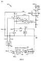
[0018] 図1は、バックコンバータ100の従来技術の実装を図示する。図1は、例示の目的のみのために示され、本開示の範囲を制限することが意図されるものではないことに留意されたい。例えば、本開示の技法が、代替のタイプのスイッチ、回路トポロジ、フィードバック構成などを組み込む他のバックコンバータの実装(図示されない)に容易に適用され得ることが理解されるだろう。このような代替の例示的な実施形態は、本開示の範囲内であることが意図される。 FIG. 1 illustrates a prior art implementation of a buck converter 100. It should be noted that FIG. 1 is shown for illustrative purposes only and is not intended to limit the scope of the present disclosure. For example, it will be appreciated that the techniques of this disclosure may be readily applied to other buck converter implementations (not shown) that incorporate alternative types of switches, circuit topologies, feedback configurations, and the like. Such alternative exemplary embodiments are intended to be within the scope of this disclosure.
[0019] 図1では、バックコンバータ100は、例えば電圧レベルVbattを生成するバッテリなどの入力と、インダクタLを交互に充電および放電するためのスイッチ制御ブロック140によって構成されるスイッチングトランジスタP1およびN1とを含む。インダクタは、負荷ZLに結合され、インダクタLからの電流は、負荷における出力電圧Voutをサポートする。P1を通る電流は、I_P1と表示されており、またN1を通る電流は、I_N1と表示されている。正電流センサ102はさらに、I_P1の正成分I_P1pを感知するために提供され、ここで、「正の」I_P1は、図1に表示されるように、P1のソースからP1のドレインの方向に流れるものとして本明細書で定義される。P1のドレインとN1とを結合するノードは、スイッチング電圧VSWをサポートする。スイッチ制御ブロック140は、下記でさらに説明されるように、例えば、制御ループのメカニズムに従ってVoutから導出される入力信号130aに基づいて、スイッチN1、P1を制御する。
In FIG. 1, the buck converter 100 includes switching transistors P1 and N1 configured by an input such as a battery that generates a voltage level Vbatt, and a
[0020] 特に、電圧感知ブロック105は、出力電圧Voutを感知し、信号105a(すなわち、「Vfb」)を生成する。増幅器110は、増幅された出力誤差信号110a(すなわち、「Verr」)を生成するために、基準電圧VrefからVfbを差し引く。Verrは、信号120a(すなわち、「ループフィルタ出力(Loop filter output)」)を生成するために、ループフィルタ120によってフィルタリングされる。ループフィルタ出力は、PWM比較器130によって、項「Ramp」と比較される。P1がオンのとき、Rampは、下記のように計算され得る(式1)。
In particular, the
Ramp=(I_P1p・Rsns1)+Slope comp+Offset
ここで、I_P1pは、P1を通る感知された正電流であり、Rsns 1は、抵抗(図1では図示されない)であり、Slope compはスロープ補償項であり、Offsetはランプオフセット項である。
Ramp = (I_P1p · Rsns1) + Slope comp + Offset
Where I_P1p is the sensed positive current through P1,
[0021] 各周期中に、P1がオフであるとき、制御ブロック140は、Rampの値をOffsetにリセットし得ることに留意されたい。特に、P1がオフであるとき、Slope comp項が制御ブロック140によって手動で(manually)リセットされ得る一方、I_P1pは自動的にゼロとなる。比較器130の出力信号130aは、パルス幅変調(PWM:pulse-width modulated)出力電圧、すなわちV_PWMでありうる。V_PWMは、スイッチ制御ブロック140に提供され、それは、それぞれトランジスタスイッチをオンおよびオフにするために、P1およびN1に関するゲート制御電圧P_ctrlおよびN_ctrlを生成する。
[0021] Note that during each cycle, when P1 is off, the
[0022]バックコンバータ出力電圧Voutは、例えば、適切に、ブロック105において分割比率を調整することによって、または基準電圧Vrefを設定することによって、目標電圧レベルに近づくように構成され得ることが理解されるだろう。Rampは、感知されたP1の電流I_P1に部分的に基づいて(例えば、式1に示されるI_P1の正成分I_P1pを通して)生成され、バックコンバータ100の制御は、「電流モード制御」のタイプとも呼ばれ得ることに留意されたい。
[0022] It is understood that the buck converter output voltage Vout may be configured to approach the target voltage level, for example, by appropriately adjusting the division ratio in
[0023] 図2は、Vfb≒Vrefのとき、例えば、バックコンバータの定常動作中に、バックコンバータ100に存在する例示的な信号波形を図示する。図2は、1つの起こりうる時間間隔中の、および1つの起こりうる動作の一定の型に対応しているバックコンバータの動作を図示することのみが意図されるものであり、示される信号間の固定のまたは通常の関係のいずれかのタイプを示唆することが意図されるものではないことに留意されたい。 FIG. 2 illustrates exemplary signal waveforms present in the buck converter 100 when Vfb≈Vref, eg, during steady state operation of the buck converter. FIG. 2 is intended only to illustrate the operation of a buck converter during one possible time interval and corresponding to a certain type of possible operation, between the signals shown. Note that it is not intended to suggest any type of fixed or normal relationship.
[0024] 図2では、バックコンバータ100はクロック信号CLKに同期され、またP1は第1の周期の始めのt1にイネーブルにされる。時間t1からt2まで、P1はオンであり、N1はオフである。この時間間隔は、TONの継続期間を有し、また、この時間中に、正電流ILを用いてインダクタを充電するために(Vbatt−Vout)の正電圧低下がLの両端に期待されるため、「充電段階(charging phase)」とも表される。充電段階中、信号Rampは、増加するインダクタ電流と、Slope compのランピング特性(ramping characteristics)のために、t1におけるレベルOffsetからt2におけるループフィルタ出力まで増加するのが見受けられる。図1を参照すると、時間t2において、Rampがループフィルタ出力未満ではなくなったとき、V_PWMは、低い電圧から高い電圧へと切り替えを行うのが見受けられる。 In FIG. 2, the buck converter 100 is synchronized with the clock signal CLK, and P1 is enabled at t1 at the beginning of the first period. From time t1 to t2, P1 is on and N1 is off. This time interval has a duration of TON, and during this time a positive voltage drop of (Vbatt−Vout) is expected across L to charge the inductor with positive current IL. , Also referred to as “charging phase”. During the charging phase, the signal Ramp is seen to increase from the level Offset at t1 to the loop filter output at t2 due to the increasing inductor current and ramping characteristics of the Slope comp. Referring to FIG. 1, at time t2, it can be seen that V_PWM switches from a low voltage to a high voltage when Ramp is no longer less than the loop filter output.
[0025] V_PWMのこの切り替えに応じて、スイッチ制御ブロック140は、N1がオンとなりP1がオフとなるように、スイッチP1、N1を再構成し、t2においてスタートする。時間t2からt3までの間隔は、TOFFの継続期間を有し且つ「放電段階(discharging phase)」に対応し、ここで、Lを通る電流ILが低下し、すなわち、ILがN1を介して接地を通って放電される。時間t2からt3までの間隔は、RampがOffsetにリセットされる間隔に対応し得ることに留意されたい。t3において、CLKの新しい周期が開始し、放電段階は、充電段階に遷移する。
In response to this switching of V_PWM, the
[0026] 図3は、図1に示されるバックコンバータ100の例示的な実装100.1を図示する。図3は、例示の目的のみのために示され、本開示の範囲を、示される正電流感知ブロックまたはバックコンバータの任意の特定の実装に限定することが意図されるものではないことに留意されたい。 [0026] FIG. 3 illustrates an exemplary implementation 100.1 of the buck converter 100 shown in FIG. It is noted that FIG. 3 is shown for illustrative purposes only and is not intended to limit the scope of the present disclosure to any particular implementation of the positive current sensing block or buck converter shown. I want.
[0027] 図3では、P1を通る正電流I_P1pを感知するために、正電流センサ102.1が提供される。特に、センサ102.1は、P1がオンにされるとき、増幅器301の負(−)の入力に正の電源電圧を結合するフィードスルーPMOSトランジスタPE1を含む。増幅器301の正(+)の入力は、P1のドレイン電圧(VSW)に結合される。この方法では、増幅器301は、PMOSトランジスタP2のゲートにおいて(VSW−Vbatt)に比例して電圧を生成する。P1を介する正のソース−ドレイン電圧低下(例えば、P1の直列のオン抵抗(series on-resistance)のため)は、そのため、301で増幅され且つP2のゲートに結合され、それは、P1を通る正電流I_P1pの関数であるドレイン電流I(I_P1p)を生成し得る。
In FIG. 3, a positive current sensor 102.1 is provided to sense a positive current I_P1p through P1. In particular, sensor 102.1 includes a feedthrough PMOS transistor PE1 that couples a positive supply voltage to the negative (-) input of
[0028] センサ102.1からの、生成された電流I(I_P1p)は、R1とR2を介する電圧V1を生成するために、電流Offsetと結合する。V1は、キャパシタC1の第1のプレートに結合される。同時に、電流ソースSlope compは、C1の第2のプレートで電圧V2を生成する。C1の第2のプレートと接地との間の電圧V2もまた、図3において「Ramp」と表示され、PWM比較器130に提供され得る電圧Rampに対応する。例えば、ブロック140によって生成された制御信号(図示されない)に基づいて、S1が各周期の開始までリセットを抑止し得るなどのように、リセットスイッチS1は、C1を介して電圧を定期的にリセットするように提供されることに留意されたい。
[0028] The generated current I (I_P1p) from the sensor 102.1 is combined with the current Offset to generate a voltage V1 through R1 and R2. V1 is coupled to the first plate of capacitor C1. At the same time, the current source Slope comp generates a voltage V2 on the second plate of C1. The
[0029] 増幅器110において基準電圧Vrefを設定することによって、またはブロック105において分割比率を感知する電圧を調整することによって、TOFFに関連するTONの継続期間は、Voutが所望された目標レベルに達するように構成されるように、調整され得ることが理解されるだろう。特に、Voutを減少させることが所望されるとき、TONは減少され得(且つTOFFは増加される)、これにより各周期で負荷へ運ばれた電流ILを減少させる。逆に、Voutが増加することが所望されるとき、TONは増加され得(且つTOFFは減少される)、これにより各周期で負荷へ運ばれた電流ILを増加させる。
[0029] By setting the reference voltage Vref at the
[0030] Voutを急速に低減させるために、N1は、Voutを放電することを可能にされる。特定の場合には、インダクタを介して印加された大きな負電圧が存在し得、それは、インダクタ電流が急速にランプダウンすることを引き起こす。N1が十分に長い継続期間にイネーブルにされる際、インダクタ電流の流れは、最終的に結局は負になり得る。バックコンバータの特定の実装では、インダクタLを通る負電流の流れを避けるために、一旦電流ILが負になると、N1は自動的にディセーブルにされ、ポイントP1およびN1は両方ともオフにされる。このイベントでは、出力電圧Voutをさらに低減させることが所望される際、他の有効な電流放電経路が利用可能でないので、出力電圧Voutを放電するために、負荷ZLが依存される(relied upon)。負荷インピーダンスZLが小さい場合、Voutが最終的な目標値に到達するには長い時間がかかり得ることに留意されたい。 [0030] In order to rapidly reduce Vout, N1 is allowed to discharge Vout. In certain cases, there can be a large negative voltage applied through the inductor, which causes the inductor current to ramp down rapidly. When N1 is enabled for a sufficiently long duration, the inductor current flow may eventually become negative eventually. In a specific implementation of the buck converter, to avoid negative current flow through inductor L, once current IL goes negative, N1 is automatically disabled and points P1 and N1 are both turned off. . In this event, when it is desired to further reduce the output voltage Vout, the load ZL is relied upon to discharge the output voltage Vout because no other effective current discharge path is available. . Note that it can take a long time for Vout to reach the final target value when the load impedance ZL is small.
[0031] 特定の実装では、Voutが低減され得るレートを増加させるために、インダクタ電流ILは、負になることを可能にされ得る。すなわち、インダクタLは、接地を通る負荷ZLからの電流ILを下げ得る。この動作のモードはまた、バックコンバータの「リバースブーストモード」または「強制的な連続状態モード(CCM:forced continuous condition mode)」として知られている。リバースブーストモード中、N1がオンであるとき、ILは、接地を通りN1を介してZLから流れ得ることに留意されたい。さらに、P1がオンであるとき、ILは、VoutからP1を通りVbattへと流れ得る。実際、N1がオンでありP1がオフであるとき、インダクタ電流は負になり、エネルギーは負荷からインダクタに搬送される。その後、N1がオフでありP1がオンであるとき、インダクタに格納されたエネルギーは、例えば、バッテリなどの入力に戻る。 [0031] In certain implementations, the inductor current IL can be allowed to become negative in order to increase the rate at which Vout can be reduced. That is, the inductor L can reduce the current IL from the load ZL passing through the ground. This mode of operation is also known as “reverse boost mode” or “forced continuous condition mode (CCM)” of the buck converter. Note that during reverse boost mode, when N1 is on, IL may flow from ZL through N1 through ground. Furthermore, when P1 is on, IL can flow from Vout through P1 to Vbatt. In fact, when N1 is on and P1 is off, the inductor current is negative and energy is transferred from the load to the inductor. Thereafter, when N1 is off and P1 is on, the energy stored in the inductor returns to the input of a battery, for example.
[0032] 図4は、Voutが第1のレベルV1から、V1を下回る第2のレベルV2に低減されるシナリオに関連付けられた過渡期間中のバックコンバータ100に存在する例示的な信号波形を図示する。特に、Vrefは、サンプリングされた電圧Vfbを下回る値に設定され、ループフィルタ出力がRampを下回るようにさせる。この場合、充電段階は、t1’からt2’までの最小継続期間TON’の間のみ継続し、この時間の間、P1がオンにされN1がオフにされるだろう。示されるこれらの事例では、TON’は、Rampとループフィルタ出力との間の関係に関わらず、P1が各周期中に常にオンであるゼロでない最小の時間間隔であることに留意されたい。 [0032] FIG. 4 illustrates an exemplary signal waveform present in the buck converter 100 during a transient period associated with a scenario where Vout is reduced from a first level V1 to a second level V2 below V1. To do. In particular, Vref is set to a value below the sampled voltage Vfb, causing the loop filter output to fall below Ramp. In this case, the charging phase will only last for a minimum duration TON 'from t1' to t2 ', during which time P1 will be turned on and N1 will be turned off. Note that in these cases shown, TON 'is the smallest non-zero time interval in which P1 is always on during each period, regardless of the relationship between Ramp and the loop filter output.
[0033] 放電段階は、t2’において始まり、t3’までの継続期間TOFF’の間、継続する。ループフィルタ出力がRampを下回るとしても、図4で示されるバックコンバータの実装100は全ての周期間で最小のオン時間TON’を課すため、TON’中はP1がオンにされることに留意されたい。図4の最小のオン時間TON’がゼロでない時間間隔であると示される一方、代替の例示的な実施形態では、ループフィルタ出力がRampを下回る全体の時間をP1がオフにされ得る場合、最小継続期間TON’はゼロになり得ることに留意されたい。さらに、図4の波形は規模(scale)に従って描かれており、またさらに、最小のオン時間TON’と周期継続期間との間の任意の特定の関係を暗示するものではないことに留意されたい。 [0033] The discharge phase begins at t2 'and continues for a duration TOFF' up to t3 '. Note that even if the loop filter output is below Ramp, the buck converter implementation 100 shown in FIG. 4 imposes a minimum on-time TON ′ between all periods, so that P1 is turned on during TON ′. I want. While the minimum on-time TON ′ of FIG. 4 is shown to be a non-zero time interval, in an alternative exemplary embodiment, if P1 can be turned off the entire time that the loop filter output falls below Ramp, the minimum Note that the duration TON ′ can be zero. Furthermore, it should be noted that the waveform of FIG. 4 is drawn according to scale and does not imply any particular relationship between the minimum on-time TON ′ and the period duration. .
[0034] 図5は、Voutの目標値が、第1のレベルV1から、V1を大幅に下回る第2のレベルV2へと減少する遷移中にバックコンバータ100に存在する例示的な電圧および電流の波形を図示する。図5の波形は、例示の目的のみのために示され、信号波形が、必ずしも示されたプロファイルを有すると示唆することが意図されるものではないことに留意されたい。 [0034] FIG. 5 illustrates exemplary voltages and currents present in the buck converter 100 during a transition in which the target value for Vout decreases from a first level V1 to a second level V2 that is significantly below V1. The waveform is illustrated. Note that the waveform of FIG. 5 is shown for illustrative purposes only and is not intended to suggest that the signal waveform necessarily has the indicated profile.
[0035] 図5では、時間T1の前に、始めに電流ILは正の値I1を有しており、対応する出力電圧Voutは第1の値V1を有している。T1において、例えば、V1からより低いレベルV2へと減少するVoutの設定ポイントに応じて、ILが減少し始める。ILは、減少するにつれて最終的に負になり、時間T2においてゼロ電流と交差する。ILが負になるとき(負荷電流がゼロであると仮定すると)、T2において、Voutは対応して減少し始める。T2の後に、対応するVoutが一旦V2を下回ると、最終的にILは増加し始め(I3と同じ位まで低く減少した後)、再度正になり得る。合わせて、Voutもまた減少し始め、最終的に時間T3周辺のその目標レベル近くに落ち着く。その後、ILおよびVoutは、Voutの目標値において、次の変化までそれらの定常レベルに(例えば、ILはI2に、またVoutはV2に)落ち着くだろう。 In FIG. 5, before the time T1, the current IL initially has a positive value I1, and the corresponding output voltage Vout has a first value V1. At T1, for example, IL begins to decrease in response to a set point of Vout that decreases from V1 to a lower level V2. IL eventually becomes negative as it decreases and crosses zero current at time T2. When IL goes negative (assuming the load current is zero), at T2, Vout begins to decrease correspondingly. After T2, once the corresponding Vout falls below V2, eventually IL begins to increase (after decreasing as low as I3) and can become positive again. Together, Vout also begins to decrease and eventually settles near its target level around time T3. IL and Vout will then settle to their steady-state level (eg, IL at I2 and Vout at V2) at the target value of Vout until the next change.
[0036] Voutを急速に低減させるためにリバースブーストモードを使用することに関連付けられる少なくとも2つの問題が存在することが、上記の説明から理解されるだろう。第1に、リバースブーストモード中、N1を通る電流ILは、際限なくますます負になり得、それは、システムの制限された電力処理能力のために、不都合な結果となり得る。第2に、下記でさらに説明されるように、システムのアンダーシュート特性のために、Voutを目標レベルまでもっていくのにかなりの追加の時間がかかり得る。 [0036] It will be appreciated from the above description that there are at least two problems associated with using the reverse boost mode to rapidly reduce Vout. First, during reverse boost mode, the current IL through N1 can become increasingly negative indefinitely, which can have adverse consequences due to the limited power handling capability of the system. Second, as will be explained further below, due to the undershoot characteristics of the system, it can take considerable additional time to bring Vout to the target level.
[0037] 特に、図5では、T1の後に、一度時間T2.1において、また再度T3において、VoutのレベルがV2の目標値と2回交差するのが見受けられる。T2.1とT3との間の継続期間では、Voutは「アンダーシュート」の状態であるとみなされることができ、ここで、Voutの過度値(transient value)は、一時的にV2の目標値を下回り、後にまたV2へと増加する。例えば、T2.1とT3との間で、再度増加し始める前に、Voutは、V3と同じ位まで低く減少し得る。このアンダーシュートは、少なくとも部分的に、T2の後に確立された大きな負電流ILのためであると見受けられる。インダクタLからの負電流を放電し、目標出力電圧V2を維持するために、正の、定常状態の電流に戻ってLを再充電するのに、かなりの時間が必要とされる。前述のシナリオは、リバースブーストモード中の電流モードのバックコンバータに関して、早くセトリング時間を得るための障害となることが理解されるだろう。 In particular, in FIG. 5, it can be seen that after T1, once at time T2.1 and again at T3, the level of Vout crosses the target value of V2 twice. In the duration between T2.1 and T3, Vout can be considered to be in an “undershoot” state, where the transient value of Vout is temporarily the target value of V2. Below and later increases to V2. For example, before starting to increase again between T2.1 and T3, Vout may decrease as low as V3. This undershoot appears to be due, at least in part, to the large negative current IL established after T2. In order to discharge the negative current from the inductor L and maintain the target output voltage V2, considerable time is required to recharge L back to the positive, steady state current. It will be appreciated that the above scenario is an obstacle to obtaining fast settling time for a current mode buck converter during reverse boost mode.
[0038] 制御ループにインダクタ電流ILについての情報をフィードバックし、また特に、アンダーシュートとセトリング時間を低減させるためにVoutが目標電圧に近づくように、ILを通る負電流の量を引き下げるための技法を提供することが望ましいだろう。 [0038] Techniques for feeding back information about the inductor current IL to the control loop and, in particular, reducing the amount of negative current through the IL so that Vout approaches the target voltage to reduce undershoot and settling time. Would be desirable to provide.
[0039] 図6は、本開示の例示的な実施形態を図示し、ここで、PMOSスイッチP1を通る負電流の流れは、バックコンバータ600の制御ループに感知およびフィードバックされる。図1および6で同様に表示されたエレメントは、特に記載されない限り、同様の機能を有するエレメントに対応し得ることに留意されたい。図6では、P1を通る負電流I_P1nの大きさを感知するために、負電流センサ602が提供される(本明細書で採用される決まりに従って、I_P1に関する負の測定された値は、正のI_P1nに対応し得る)。示された例示的な実施形態では、負電流センサ602の出力I_P1nは、比較器130のための「Adjusted ramp」信号を生成するために使用され、ここで、Adjusted rampは、P1がオンであるときに下記のように定義される(式2)。
[0039] FIG. 6 illustrates an exemplary embodiment of the present disclosure, where the negative current flow through the PMOS switch P1 is sensed and fed back to the control loop of the
Adjusted ramp=(I_P1p・Rsns 1)−(I_P1n・Rsns 2)+Slope comp+Offset
ここで、I_P1nはP1を通る感知された負電流であり、Rsns 2は抵抗(図6で図示されない)である。式2と式1との比較から、インダクタ電流ILが正であるとき、Adjusted rampは、Rampと等しいことが理解されるだろう。しかしながら、ILが負であるとき、Adjusted rampは、項(I_P1n・Rsns2)のために、Rampよりも小さくなり得る。加えて、Adjusted rampは、ILがより負になるにつれて、Rampをますます下回り得る。
Adjusted ramp = (I_P1p · Rsns 1) − (I_P1n · Rsns 2) + Slope comp + Offset
Where I_P1n is the sensed negative current through P1, and
[0040] 従って、図6から、比較器130の正(+)の入力端子におけるAdjusted rampのより低い値は、Rampの対応する値よりもより長いTON/より短いTOFFでPWM出力電圧130aを生成し得ることが理解されるだろう。言い換えると、式2でAdjusted rampを使用することで、PMOSのオン時間は、インダクタ電流ILがますます負になるにつれて次第に増加し、それは結果として、ILがさらに際限なくますます負になることを回避する。
Thus, from FIG. 6, a lower value of Adjusted ramp at the positive (+) input terminal of the
[0041] 図7は、VoutがV1からV2へ遷移する期間中にバックコンバータ600に存在する例示的な信号波形を図示し、ここで、P1を通る負電流は、上述された制御ループへフィードバックとして提供される。図7は、例示の目的のためのみに示され、本開示の範囲を、示される任意の例示的な信号波形に制限することが意図されるものではないことに留意されたい。
[0041] FIG. 7 illustrates an exemplary signal waveform present in the
[0042] 図7では、Adjusted rampが破線で示されている。示される時間間隔(例えば、t1*の前からt6*の後まで)は、VoutがV1からV2へ遷移している時間の期間に対応し、特に、負電流は、インダクタLを通って流れる。これらの時間中、P1がオンであるとき、I_P1nは正の大きさ(positive magnitude)を有し(負のILが検出されるため)、そのため、Adjusted rampは、式2に従って、対応して低減され得る。例えば、図7では、時間t1*とt2*との間の継続期間TON*について、P1はオンであり、Adjusted rampは、t1*の前のループフィルタ出力を上回るレベルOffsetから、t1*におけるループフィルタ出力を下回るレベルまで減少するのが見受けられる。t2*の後に、t2*とt3*との間の継続期間TOFF*の間、P1はオフであり、N1はオンである。t3*において、この周期が繰り返される。
In FIG. 7, Adjusted ramp is indicated by a broken line. The time interval shown (eg, from before t1 * to after t6 * ) corresponds to the period of time during which Vout transitions from V1 to V2, and in particular, negative current flows through inductor L. During these times, when P1 is on, I_P1n has a positive magnitude (because negative IL is detected), so Adjusted ramp is correspondingly reduced according to
[0043] 図8は、VoutにおけるV1からV2への遷移中にバックコンバータ600に存在する例示的な電圧および電流の波形を図示し、ここで、P1を通る負電流は、本開示に従った制御ループを調整するように使用される。図8の波形は、例示の目的のみのために示され、信号波形が、必ずしも示されたプロファイルを有すると示唆することが意図されるものではないことに留意されたい。図5および8で同様に表示された変数は、特に記載されない限り、同様の値を有し得ることに留意されたい。例えば、図8のV1およびV2の例示的なレベルは、図5を参照して説明される同じレベルに対応し得る。
[0043] FIG. 8 illustrates exemplary voltage and current waveforms present in the
[0044] 図8では、図5と同様に、T1において始めに電流ILは正の値I1を有しており、対応する出力電圧Voutは第1の値V1を有している。T1において、例えば、V1からより低いレベルV2へと減少するVoutの設定ポイントに応じて、ILが減少し始める。ILは、減少するにつれて最終的に負になり、時間T2においてゼロと交差する。ILが負になるとき、センサ602によって感知されるようなI_P1nは、正であり得る。上記で初めに説明されるように、正のI_P1nは、Rampに関連するAdjusted rampを減少させ、そのため、図5でプロファイリングされた実装に関連する、P1がオンにされる時間TON*を増加させる。ILは、I2へと再度増加する前に、I3*と同じ位まで低く減少する。
In FIG. 8, similarly to FIG. 5, at time T1, the current IL has a positive value I1, and the corresponding output voltage Vout has the first value V1. At T1, for example, IL begins to decrease in response to a set point of Vout that decreases from V1 to a lower level V2. IL eventually becomes negative as it decreases and crosses zero at time T2. When IL goes negative, I_P1n as sensed by
[0045] Adjusted rampにおける項I_P1nの存在のために、I3*は、図5で示される負電流I3を大幅に上回る(すなわち、それより負ではない)ことが理解されるだろう。これに対応して、Voutは、時間T3*においてV2の目標値に落ち着くのが見受けられ、それは、図5に描かれた実装に対応する時間T3よりも、大幅に早いものである。そのため、V1からV2への遷移に必要とされる時間は、バックコンバータ100に関してよりも、バックコンバータ600に関しての方が、かなり短くなり得ることが上記の説明から理解されるだろう。
[0045] It will be appreciated that due to the presence of the term I_P1n in the Adjusted ramp, I3 * is significantly greater (ie, less negative) than the negative current I3 shown in FIG. Correspondingly, Vout is seen to settle to the target value of V2 at time T3 * , which is significantly faster than time T3 corresponding to the implementation depicted in FIG. Thus, it will be appreciated from the above description that the time required for the transition from V1 to V2 can be significantly shorter for the
[0046] 本明細書で説明される技法の利点は、説明される方法において式2でAdjusted rampを生成するために負のP1電流I_P1nを組み込むことによって、例えばスイッチ制御ブロック140などによって組み込まれた同じ制御ロジックが最小の修正で再利用されることができ、それにより制御システムに対してもたらす追加の複雑さが最小であることであると理解されるだろう。特に、線形かつ連続した制御技法は、バックコンバータ100に採用され得る。さらに、有利なことに、制御システムは、「フォワードバック(forward buck)」と「リバースブースト」との別個の状態の間でスイッチングを適応させることを必要としておらず、それにより、システムの安定性を改善している。
[0046] The advantages of the techniques described herein were incorporated by, for example,
[0047] 図9は、バックコンバータ600の例示的な実装600.1を図示する。図9は、例示の目的のみのために示され、本開示の範囲を、図6で示されたバックコンバータ600の例示的な実施形態のみに制限することが意図されるものではないことに留意されたい。
[0047] FIG. 9 illustrates an exemplary implementation 600.1 of the
[0048] 図9では、図6のセンサ602が、VSWを増幅器910の正(+)の入力に結合するフィードスルーPMOSトランジスタPE2を含む回路602.1を使用して実装される。増幅器910の負(−)の入力は、Vbattに結合される。この方法では、増幅器910は、ドレインがPE2のドレインに結合されるNMOSトランジスタN2のゲートにおいて(VSW−Vbatt)に比例して電圧を生成する。N2のゲート電圧はさらに、NMOSトランジスタN3に提供され、ドレインがノード699にも結合され、また「負電流」トランジスタを意味している。ノード699は、結果として、R2を介してV3’に結合され、ここで、V3’はまた、正電流センサ102.1の出力に結合される。ノード699はさらに、R3を介してV1’に結合され、V1’は、Offset電流ソース、C1およびスイッチS1に結合される。
In FIG. 9, the
[0049] 特に、リバースブーストモード中、VSWは、P1がオンであるとき、Vbattを上回ることが予期され、そのため、N3がオンにされることが予期され、指示された極性を有する、負のP1電流の一次関数(linear function)であるドレイン電流(I_P1n)を生成する。I(I_P1n)は、そうでなければレジスタR1およびR2を通って流れ得るI(I_P1p)および電流Offsetから差し引かれるのが見受けられ、そのため、キャパシタC1の第1のプレートにおける電圧V1’は、I(I_P1n)の結果に対応して低くなることが予期される。 [0049] In particular, during reverse boost mode, VSW is expected to exceed Vbatt when P1 is on, so N3 is expected to be turned on and has the indicated polarity, negative A drain current (I_P1n) that is a linear function of the P1 current is generated. It can be seen that I (I_P1n) is subtracted from I (I_P1p) and current Offset, which can otherwise flow through resistors R1 and R2, so that the voltage V1 ′ on the first plate of capacitor C1 is I It is expected to decrease corresponding to the result of (I_P1n).
[0050] 図10は、本開示に従った方法1000の例示的な実施形態を図示する。方法1000は、例示の目的のみのために示され、本開示の範囲を限定することが意図されるものではないことに留意されたい。
[0050] FIG. 10 illustrates an exemplary embodiment of a
[0051] ブロック1010において、インダクタの第1のノードが電源電圧に選択的に結合される。
[0051] At
[0052] ブロック1020において、インダクタの第1のノードが接地に選択的に結合される。
[0052] At
[0053] ブロック1030において、この選択的な結合が、インダクタの第2のノードに結合される負荷における出力電力を設定するように構成される。この構成は、フィルタリングされた誤差電圧を調整されたランプ電圧と比較することを備え得る。
[0053] At
[0054] ブロック1040において、負電流は、インダクタを通って感知され、ここで、調整されたランプ電圧は、感知された負電流に応じて調整されたランプ電圧を低減させる付加的な項を備える。
[0054] In
[0055] PMOSトランジスタがVbattにインダクタLを結合する充電スイッチ(例えば、図6の例示的な実施形態600において)として使用される、例示的な実施形態が上記で説明されている一方、説明された技法は、充電スイッチに関してPMOSトランジスタ以外のエレメントを用いる代替の例示的な実施形態において容易に利用され得ることに留意されたい。例えば、代替の例示的な実施形態(図示されない)ではまた、NMOSスイッチが利用され、NMOS(充電)スイッチを通る負電流が本明細書で説明される技法で感知および利用され得る。このような代替の例示的な実施形態は、本開示の範囲内であることが意図される。
[0055] While an exemplary embodiment is described above, a PMOS transistor is used as a charge switch (eg, in the
[0056] バックコンバータを組み込む任意のアプリケーションのタイプが本開示の技法を利用し得ることが理解されるだろう。例えば、特定の例示的な実施形態では、本開示で説明された技法に組み込まれるバックコンバータは、従来技術において周知である、平均電力追跡(APT:average power tracking)スキーム、スイッチモードバッテリチャージャ(SMBC:switched-mode battery chargers)、および高速過渡供給(FTS:fast transient supply)スキームに適用され得る。このような例示的な実施形態は、本開示の範囲内であることが意図される。 [0056] It will be appreciated that any type of application that incorporates a buck converter may utilize the techniques of this disclosure. For example, in certain exemplary embodiments, a buck converter that is incorporated into the techniques described in this disclosure is an average power tracking (APT) scheme, switch mode battery charger (SMBC), which is well known in the prior art. : Switched-mode battery chargers) and fast transient supply (FTS) schemes. Such exemplary embodiments are intended to be within the scope of this disclosure.
[0057] 本明細書および請求項では、エレメントが別のエレメントに「接続される」または「結合される」と記載されるとき、それが他のエレメントに直接接続または結合されることができるか、または介在するエレメントが存在し得ることが理解されるだろう。対照的に、エレメントが別のエレメントに「直接接続される」または「直接結合される」と記載されるとき、介在するエレメントは存在しない。加えて、エレメントが別のエレメントに「電気的に結合される」と記載されるとき、それは、低い抵抗の経路がこのようなエレメント間で存在することを表す一方、エレメントが別のエレメントと単に「結合される」と記載されるとき、このようなエレメント間に低い抵抗の経路が存在するかしないかはわからない。 [0057] In this specification and claims, when an element is described as "connected" or "coupled" to another element, can it be directly connected or coupled to the other element? It will be understood that there may be intervening elements. In contrast, when an element is described as being “directly connected” or “directly coupled” to another element, there are no intervening elements present. In addition, when an element is described as “electrically coupled” to another element, it represents that a low resistance path exists between such elements, while the element is simply connected to another element. When described as “coupled”, it is not known whether there is a low resistance path between such elements.
[0058] 当業者は、情報および信号が、様々な異なる技術および技法のいずれかを使用して表され得ることを理解するだろう。例えば、上記の説明を通して参照されうるデータ、命令、コマンド、情報、信号、ビット、シンボル、およびチップは、電圧、電流、電磁波、磁界または磁気粒子、光学界または光学粒子、あるいはそれらの任意の組み合わせによって表わされうる。 [0058] Those of skill in the art will understand that information and signals may be represented using any of a variety of different technologies and techniques. For example, data, instructions, commands, information, signals, bits, symbols, and chips that may be referred to throughout the above description are voltages, currents, electromagnetic waves, magnetic fields or magnetic particles, optical fields or optical particles, or any combination thereof Can be represented by
[0059] 当業者はさらに、本明細書に開示された例示的な態様に関連して説明された様々な例示的な論理ブロック、モジュール、回路、およびアルゴリズムステップが、電子ハードウェア、コンピュータソフトウェア、または両方の組み合わせとして実装されうることを理解するだろう。ハードウェアおよびソフトウェアのこの互換性を明確に例示するために、様々な例示的コンポーネント、ブロック、モジュール、回路、およびステップが、一般にそれらの機能の観点から上記で説明されている。このような機能が、ハードウェアとして実装されるか、またはソフトウェアとして実装されるかは、特定のアプリケーションおよびシステム全体に課せられる設計制約に依存する。当業者は、各特定のアプリケーションに関して、様々な方法で、説明された機能を実装し得るが、このような実装の決定は、本発明の例示的な態様の範囲から逸脱を引き起こしていると解釈されるべきではない。 [0059] Those skilled in the art further understand that the various exemplary logic blocks, modules, circuits, and algorithm steps described in connection with the exemplary aspects disclosed herein are electronic hardware, computer software, It will be understood that or may be implemented as a combination of both. To clearly illustrate this interchangeability of hardware and software, various illustrative components, blocks, modules, circuits, and steps have been described above generally in terms of their functionality. Whether such functionality is implemented as hardware or software depends upon the particular application and design constraints imposed on the overall system. One skilled in the art may implement the described functionality in a variety of ways for each particular application, but such implementation decisions are interpreted as causing deviations from the scope of the exemplary aspects of the invention. Should not be done.
[0060] 本明細書に開示された例示的な実施形態に関連して説明される様々な実例となる論理ブロック、モジュール、および回路は、汎用プロセッサ、デジタル信号プロセッサ(DSP)、特定用途向け集積回路(ASIC)、フィールドプログラマブルゲートアレイ(FPGA)、または他のプログラマブル論理デバイス、ディスクリートゲートまたはトランジスタロジック、ディスクリートハードウェアコンポーネント、あるいは本明細書で説明される機能を実行するように設計されたこれらの任意の組み合わせで、実装または実行されうる。汎用プロセッサはマイクロプロセッサであり得るが、代替としてプロセッサは任意の従来のプロセッサ、コントローラ、マイクロコントローラ、またはステートマシンであり得る。プロセッサはまた、例えば、DSPと、1つのマクロプロセッサ、複数のマイクロプロセッサ、DSPコアに結合した1つまたは複数のマイクロプロセッサ、あるいは任意の他のこれらの構成との組み合わせなどの、計算デバイスの組み合わせとして実装されうる。 [0060] Various illustrative logic blocks, modules, and circuits described in connection with the exemplary embodiments disclosed herein are general purpose processors, digital signal processors (DSPs), application specific integrations. Circuit (ASIC), field programmable gate array (FPGA), or other programmable logic device, discrete gate or transistor logic, discrete hardware components, or these designed to perform the functions described herein It can be implemented or implemented in any combination. A general purpose processor may be a microprocessor, but in the alternative, the processor may be any conventional processor, controller, microcontroller, or state machine. A processor is also a combination of computing devices, such as, for example, a combination of a DSP with one macro processor, a plurality of microprocessors, one or more microprocessors coupled to a DSP core, or any other of these configurations. Can be implemented as
[0061] 本明細書で開示された例示的な態様に関連して説明された方法またはアルゴリズムのステップは、直接ハードウェアにおいて、プロセッサによって実行されるソフトウェアモジュールにおいて、またはこれら2つの組み合わせにおいて、具現化されうる。ソフトウェアモジュールは、ランダムアクセスメモリ(RAM)、フラッシュメモリ、読み出し専用メモリ(ROM)、電気的プログラマブルROM(EPROM)、電気的消去可能プログラマブルROM(EEPROM(登録商標))、レジスタ、ハードディスク、リムーバルディスク、CD−ROM、または当該技術分野において周知である任意の他の形状の記憶媒体において存在しうる。例示的な記憶媒体は、プロセッサがこの記憶媒体から情報を読み取り、またこの記憶媒体に情報を書き込むことができるように、プロセッサに結合される。代替として、記憶媒体はプロセッサに統合され得る。プロセッサおよび記憶媒体は、ASICに存在し得る。ASICは、ユーザ端末に存在し得る。代替として、プロセッサおよび記憶媒体は、ユーザ端末において個別の構成要素として存在し得る。 [0061] Method or algorithm steps described in connection with the exemplary aspects disclosed herein may be implemented directly in hardware, in software modules executed by a processor, or in a combination of the two. Can be realized. Software modules include random access memory (RAM), flash memory, read only memory (ROM), electrically programmable ROM (EPROM), electrically erasable programmable ROM (EEPROM (registered trademark)), registers, hard disk, removable disk, It may be present on a CD-ROM or any other form of storage medium well known in the art. An exemplary storage medium is coupled to the processor such that the processor can read information from, and write information to, the storage medium. In the alternative, the storage medium may be integral to the processor. A processor and a storage medium may reside in the ASIC. The ASIC may exist in the user terminal. In the alternative, the processor and the storage medium may reside as discrete components in a user terminal.
[0062] 1つまたは複数の例示的な態様では、説明された機能は、ハードウェア、ソフトウェア、ファームウェア、またはこれらの任意の組み合わせで実装されうる。ソフトウェアで実装される場合、機能は、コンピュータ読取可能媒体上で、1つまたは複数の命令またはコードとして送信または記憶されうる。コンピュータ読取可能媒体は、1つの場所から別の場所へのコンピュータプログラムの転送を容易にする任意の媒体を含む通信媒体とコンピュータ記憶媒体との両方を含む。記憶媒体は、コンピュータによってアクセスできる任意の利用可能な媒体であり得る。限定ではなく例として、このようなコンピュータ読取可能媒体は、RAM、ROM、EEPROM、CD−ROMまたは他の光ディスク記憶装置、磁気ディスク記憶装置またはその他の磁気記憶デバイス、あるいは、データ構造または命令の形式で所望されたプログラムコードを記憶または搬送するために使用可能であり、かつコンピュータによってアクセスされることができる任意の他の媒体を備え得る。また、任意の接続は、コンピュータ読み取り可能な媒体と厳密には称されうる。例えば、ソフトウェアが、同軸ケーブル、光ファイバーケーブル、ツイストペア、デジタル加入者回線(DSL)、または赤外線、無線、およびマイクロ波のようなワイヤレス技術を使用して、ウェブサイト、サーバ、または他の遠隔ソースから送信される場合、同軸ケーブル、光ファイバーケーブル、ツイストペア、DSL、または赤外線、無線、およびマイクロ波のようなワイヤレス技術は、媒体の定義に含まれる。本明細書で使用される場合、ディスク(disk)およびディスク(disc)は、コンパクトディスク(CD)、レーザーディスク(登録商標)、光ディスク、デジタル多目的ディスク(DVD)、フロッピー(登録商標)ディスクおよびブルーレイ(登録商標)ディスクを含み、ここで、ディスク(disks)が通常磁気的にデータを再生する一方、ディスク(discs)は、レーザーを用いて光学的にデータを再生する。上記の組み合わせもまた、コンピュータ読取可能な媒体の範囲内に含まれるべきである。 [0062] In one or more exemplary aspects, the functions described may be implemented in hardware, software, firmware, or any combination thereof. If implemented in software, the functions may be transmitted or stored as one or more instructions or code on a computer-readable medium. Computer-readable media includes both communication media and computer storage media including any medium that facilitates transfer of a computer program from one place to another. A storage media may be any available media that can be accessed by a computer. By way of example, and not limitation, such computer-readable media may be RAM, ROM, EEPROM, CD-ROM or other optical disk storage device, magnetic disk storage device or other magnetic storage device, or data structure or form of instructions Any other medium that can be used to store or carry the desired program code and that can be accessed by a computer may be provided. Also, any connection may be strictly referred to as a computer readable medium. For example, software can use a coaxial cable, fiber optic cable, twisted pair, digital subscriber line (DSL), or wireless technology such as infrared, wireless, and microwave from a website, server, or other remote source When transmitted, coaxial technologies, fiber optic cables, twisted pair, DSL, or wireless technologies such as infrared, radio, and microwave are included in the definition of media. As used herein, disk and disc are compact disc (CD), laser disc (registered trademark), optical disc, digital multipurpose disc (DVD), floppy disc and Blu-ray. (Registered trademark) discs, where the discs normally reproduce data magnetically, while the discs optically reproduce data using a laser. Combinations of the above should also be included within the scope of computer-readable media.
[0063] 開示された例示的な態様の上記説明は、いずれの当業者も、本発明の製造または使用が可能であるように提供される。これらの例示的な態様への様々な修正は、当業者にとって容易に明らかであり、本明細書に定義された一般的な原理は、本発明の精神または範囲から逸脱することなく、他の例示的な態様にも適用され得る。したがって、本開示は、本明細書に示された態様に制限されることが意図されるものではなく、本明細書に開示される原理および新規の特徴と一致する最も広い範囲を与えられるべきものである。
以下に本願発明の当初の特許請求の範囲に記載された発明を付記する。
[C1]
装置であって、
電源電圧にインダクタの第1のノードを選択的に結合するように構成された充電スイッチと、
接地に前記インダクタの前記第1のノードを選択的に結合するように構成された放電スイッチと、
前記インダクタの第2のノードに結合された負荷における出力電圧を設定するために前記充電スイッチおよび前記放電スイッチを制御するように構成された制御ブロックと、ここで、前記制御ループは、フィルタリングされた誤差電圧を調整されたランプ電圧と比較する比較器を備える、
前記インダクタを通る負電流を感知するように構成された負電流感知ブロックと、
を備え、
前記調整されたランプ電圧は、感知された負電流に応じて前記調整されたランプ電圧を低減させる付加的な項を備える、装置。
[C2]
前記インダクタを通る正電流を感知するための正電流感知ブロックをさらに備え、前記調整されたランプ電圧はさらに、感知された正電流に応じて前記調整されたランプ電圧を増加させる付加的な項を備える、C1に記載の装置。
[C3]
前記充電スイッチは、PMOSトランジスタを備え、前記放電スイッチは、NMOSトランジスタを備える、C1に記載の装置。
[C4]
前記負電流感知ブロックは、前記充電スイッチを通る負電流を感知するように構成される、C1に記載の装置。
[C5]
前記負電流感知ブロックは、負のインダクタ電流に対応する、前記充電スイッチの両端の電圧低下を感知するように構成された増幅器を備える、C4に記載の装置。
[C6]
前記負電流感知ブロックはさらに、
前記充電スイッチの制御電圧に結合されるフィードスルートランジスタと、ここにおいて、前記増幅器は、前記フィードスルートランジスタに結合される入力端子を有し、
負電流トランジスタに結合された前記増幅器の前記出力と、
を備え、
前記負電流トランジスタは、前記調整されたランプ電圧に比例する電流を生成するための回路に結合されるドレインを有する、
C5に記載の装置。
[C7]
前記調整されたランプ電圧に比例する電流を生成するための前記回路は、オフセット電流ソース、キャパシタC1、およびスロープ補償電流ソースを備える、C6に記載の装置。
[C8]
前記充電スイッチは、NMOSトランジスタを備える、C1に記載の装置。
[C9]
前記制御ブロックは、前記出力電圧を設定するために、線形かつ連続した制御ループシステムを実装するように構成される、C1に記載の装置。
[C10]
前記スイッチ、制御ブロック、および負電流感知ブロックは、バックコンバータに組み込まれ、前記バックコンバータは、平均電力追跡スキーム、スイッチモード充電器に使用されるか、または高速過渡供給バックコンバータとして使用される、C1に記載の装置。
[C11]
方法であって、
電源電圧にインダクタの第1のノードを選択的に結合することと、
接地に前記インダクタの前記第1のノードを選択的に結合することと、
前記インダクタの第2のノードに結合された負荷における出力電圧を設定するために前記選択的な結合を構成することと、ここで、前記構成することは、フィルタリングされた誤差電圧を調整されたランプ電圧と比較することを備える、
前記インダクタを通る負電流を感知することと、
を備え、
前記調整されたランプ電圧は、感知された負電流に応じて低減される、方法。
[C12]
前記インダクタを通る正電流を感知すること
をさらに備え、
前記調整されたランプ電圧は、感知された正電流に応じて増加される、C11に記載の方法。
[C13]
前記インダクタを通る前記負電流を前記感知することは、前記電源電圧に前記インダクタの前記第1のノードを選択的に結合するために充電スイッチを通る負電流を感知することを備える、C11に記載の方法。
[C14]
前記負電流を感知することは、前記充電スイッチの両端の電圧低下を感知することを備える、C13に記載の方法。
[C15]
前記充電スイッチは、PMOSトランジスタを備える、C13に記載の方法。
[C16]
前記充電スイッチが前記電源電圧に前記インダクタの前記第1のノードを結合することを可能にする時間間隔の間に、充電スイッチを通る前記負電流を前記感知することが実行される、C13に記載の方法。
[C17]
装置であって、
電源電圧にインダクタの第1のノードを選択的に結合するための手段と、
接地に前記インダクタの前記第1のノードを選択的に結合するための手段と、
前記インダクタの第2のノードに結合された負荷における出力電圧を設定するために前記選択的な結合を構成するための手段と、ここで、前記構成することは、フィルタリングされた誤差電圧を調整されたランプ電圧と比較することを備える、
前記インダクタを通る負電流を感知するための手段と
を備える、装置。
[C18]
前記インダクタを通る正電流を感知するための手段をさらに備える、C17に記載の装置。
[C19]
前記インダクタを通る負電流を感知するための前記手段は、前記充電スイッチを通る負電流を感知するための手段をさらに備える、C17に記載の装置。
[C20]
前記充電スイッチを通る負電流を感知するための前記手段は、前記充電スイッチの両端の電圧低下を感知するための手段を備える、C19に記載の装置。
[0063] The previous description of the disclosed exemplary embodiments is provided to enable any person skilled in the art to make or use the present invention. Various modifications to these exemplary embodiments will be readily apparent to those skilled in the art, and the generic principles defined herein may be used in other examples without departing from the spirit or scope of the invention. It can also be applied to other aspects. Accordingly, this disclosure is not intended to be limited to the embodiments shown herein but is to be accorded the widest scope consistent with the principles and novel features disclosed herein. It is.
The invention described in the scope of the claims of the present invention is appended below.
[C1]
A device,
A charge switch configured to selectively couple the first node of the inductor to a power supply voltage;
A discharge switch configured to selectively couple the first node of the inductor to ground;
A control block configured to control the charge switch and the discharge switch to set an output voltage at a load coupled to a second node of the inductor, wherein the control loop is filtered Comprising a comparator for comparing the error voltage with the adjusted lamp voltage;
A negative current sensing block configured to sense negative current through the inductor;
With
The adjusted lamp voltage comprises an additional term that reduces the adjusted lamp voltage in response to a sensed negative current.
[C2]
The method further comprises a positive current sensing block for sensing a positive current through the inductor, the regulated lamp voltage further comprising an additional term that increases the regulated lamp voltage in response to the sensed positive current. The apparatus of C1, comprising.
[C3]
The apparatus according to C1, wherein the charge switch comprises a PMOS transistor and the discharge switch comprises an NMOS transistor.
[C4]
The apparatus of C1, wherein the negative current sensing block is configured to sense a negative current through the charge switch.
[C5]
The apparatus of C4, wherein the negative current sensing block comprises an amplifier configured to sense a voltage drop across the charge switch corresponding to a negative inductor current.
[C6]
The negative current sensing block further includes
A feedthrough transistor coupled to a control voltage of the charge switch, wherein the amplifier has an input terminal coupled to the feedthrough transistor;
The output of the amplifier coupled to a negative current transistor;
With
The negative current transistor has a drain coupled to a circuit for generating a current proportional to the regulated lamp voltage;
The device according to C5.
[C7]
The apparatus of C6, wherein the circuit for generating a current proportional to the adjusted ramp voltage comprises an offset current source, a capacitor C1, and a slope compensation current source.
[C8]
The apparatus according to C1, wherein the charge switch comprises an NMOS transistor.
[C9]
The apparatus of C1, wherein the control block is configured to implement a linear and continuous control loop system to set the output voltage.
[C10]
The switch, control block, and negative current sensing block are incorporated into a buck converter, which is used for an average power tracking scheme, a switch mode charger, or used as a fast transient supply buck converter. The device according to C1.
[C11]
A method,
Selectively coupling the first node of the inductor to the power supply voltage;
Selectively coupling the first node of the inductor to ground;
Configuring the selective coupling to set an output voltage at a load coupled to a second node of the inductor, wherein the configuring comprises a filtered ramp with a filtered error voltage Comprising comparing with voltage,
Sensing negative current through the inductor;
With
The adjusted lamp voltage is reduced in response to a sensed negative current.
[C12]
Sensing positive current through the inductor
Further comprising
The method of C11, wherein the regulated lamp voltage is increased in response to a sensed positive current.
[C13]
The sensing of the negative current through the inductor comprises sensing a negative current through a charge switch to selectively couple the first node of the inductor to the power supply voltage. the method of.
[C14]
The method of C13, wherein sensing the negative current comprises sensing a voltage drop across the charge switch.
[C15]
The method of C13, wherein the charge switch comprises a PMOS transistor.
[C16]
C13, wherein the sensing is performed for the negative current through a charge switch during a time interval that allows the charge switch to couple the first node of the inductor to the power supply voltage. the method of.
[C17]
A device,
Means for selectively coupling the first node of the inductor to a power supply voltage;
Means for selectively coupling the first node of the inductor to ground;
Means for configuring the selective coupling to set an output voltage at a load coupled to a second node of the inductor, wherein the configuring is adjusted for a filtered error voltage. Comparing with the lamp voltage
Means for sensing negative current through the inductor;
An apparatus comprising:
[C18]
The apparatus of C17, further comprising means for sensing a positive current through the inductor.
[C19]
The apparatus of C17, wherein the means for sensing negative current through the inductor further comprises means for sensing negative current through the charge switch.
[C20]
The apparatus of C19, wherein the means for sensing a negative current through the charge switch comprises means for sensing a voltage drop across the charge switch.
Claims (17)
電源電圧にインダクタの第1のノードを選択的に結合するように構成された充電スイッチと、
接地に前記インダクタの前記第1のノードを選択的に結合するように構成された放電スイッチと、
ランプ電圧を生成するように構成された回路と、
前記ランプ電圧に基づいて前記インダクタの第2のノードに結合された負荷における出力電圧を設定するために前記充電スイッチおよび前記放電スイッチを制御するように構成された制御ブロックと、
前記インダクタを通る正電流を感知するための正電流感知ブロックと、ここにおいて、前記回路は、感知された前記正電流に基づいて前記ランプ電圧を生成するように構成される、
前記インダクタを通る負電流を感知するように構成された負電流感知ブロックと、ここにおいて、前記回路は、前記インダクタを通る前記負電流の感知に応じて前記ランプ電圧を調整するようにさらに構成される、
を備え、前記回路は、第1の端子および第2の端子を有する一連のレジスタを備え、前記回路は、前記第1の端子を介して前記正電流感知ブロックの出力を結合し、前記第2の端子を介して前記負電流感知ブロックの出力を結合するように構成される、装置。 A device,
A charge switch configured to selectively couple the first node of the inductor to a power supply voltage;
A discharge switch configured to selectively couple the first node of the inductor to ground;
A circuit configured to generate a ramp voltage;
A control block configured to control the charge switch and the discharge switch to set an output voltage at a load coupled to a second node of the inductor based on the lamp voltage ;
A positive current sensing block for sensing a positive current through the inductor, wherein the circuit is configured to generate the lamp voltage based on the sensed positive current;
A negative current sensing block configured to sense negative current through the inductor , wherein the circuit is further configured to adjust the lamp voltage in response to sensing the negative current through the inductor. The
The circuit comprises a series of registers having a first terminal and a second terminal , the circuit coupling the output of the positive current sensing block via the first terminal, and the second Ru is configured via the terminals to couple the output of the negative current sensing block device.
前記充電スイッチの制御電圧に結合されるフィードスルートランジスタ、ここにおいて、前記増幅器は、前記フィードスルートランジスタに結合される入力端子を有する、
を備え、前記増幅器の出力は、負電流トランジスタに結合され、
前記負電流トランジスタは、前記調整されたランプ電圧に比例する電流を生成するための回路に結合されるドレインを有する、請求項4に記載の装置。 The negative current sensing block further includes
Feed scan route Rungis data that is coupled to the control voltage of the charging switch, wherein the amplifier is closed the input terminal coupled to the feed-through transistor,
The output of the amplifier is coupled to a negative current transistor ;
The apparatus of claim 4 , wherein the negative current transistor has a drain coupled to a circuit for generating a current proportional to the regulated ramp voltage.
電源電圧にインダクタの第1のノードを選択的に結合することと、
接地に前記インダクタの前記第1のノードを選択的に結合することと、
第1の端子および第2の端子を有する一連のレジスタを介してランプ電圧を生成することと、
前記ランプ電圧に基づいて前記インダクタの第2のノードに結合された負荷における出力電圧を設定するために前記選択的な結合を構成することと、
前記インダクタを通る負電流を感知することと、
前記インダクタを通る正電流を感知することと、
前記感知された正電流に基づく第1の電流を前記第1の端子に結合することと、
前記感知された負電流に基づく第2の電流を前記第2の端子に結合することと、
前記インダクタを通る前記負電流の前記感知に応じて前記ランプ電圧を調整することと
を備える、方法。 A method,
Selectively coupling the first node of the inductor to the power supply voltage;
Selectively coupling the first node of the inductor to ground;
Generating a ramp voltage through a series of resistors having a first terminal and a second terminal;
Configuring the selective coupling to set an output voltage at a load coupled to a second node of the inductor based on the ramp voltage ;
Sensing negative current through the inductor;
Sensing a positive current through the inductor;
Coupling a first current based on the sensed positive current to the first terminal;
Coupling a second current based on the sensed negative current to the second terminal;
Adjusting the lamp voltage in response to the sensing of the negative current through the inductor ;
Ru with a, way.
充電スイッチを通る電源電圧にインダクタの第1のノードを選択的に結合するための手段と、
接地に前記インダクタの前記第1のノードを選択的に結合するための手段と、
第1の端子および第2の端子を有する一連のレジスタを介してランプ電圧を生成するための手段と、
前記ランプ電圧に基づいて前記インダクタの第2のノードに結合された負荷における出力電圧を設定するために前記選択的な結合を構成するための手段と、
前記インダクタを通る正電流を感知し、前記第1の端子に結合された第1の電流を出力するための手段と、
前記インダクタを通る負電流を感知し、前記第2の端子に結合された第2の電流を出力するための手段と、ここにおいて、前記ランプ電圧を前記生成するための手段は、前記インダクタを通る前記負電流の感知に応じて前記ランプ電圧を調整する、
を備える、装置。 A device,
Means for selectively coupling the first node of the inductor to a power supply voltage through the charge switch ;
Means for selectively coupling the first node of the inductor to ground;
Means for generating a ramp voltage through a series of resistors having a first terminal and a second terminal;
Means for configuring the selective coupling to set an output voltage at a load coupled to a second node of the inductor based on the ramp voltage ;
Means for sensing a positive current through the inductor and outputting a first current coupled to the first terminal;
Means for sensing a negative current through the inductor and outputting a second current coupled to the second terminal , wherein the means for generating the ramp voltage passes through the inductor. Adjusting the lamp voltage in response to sensing the negative current;
An apparatus comprising:
Applications Claiming Priority (3)
| Application Number | Priority Date | Filing Date | Title |
|---|---|---|---|
| US13/752,197 US9442503B2 (en) | 2013-01-28 | 2013-01-28 | Negative current sense feedback for reverse boost mode |
| US13/752,197 | 2013-01-28 | ||
| PCT/US2014/012392 WO2014116607A1 (en) | 2013-01-28 | 2014-01-21 | Negative current sense feedback for reverse boost mode |
Publications (3)
| Publication Number | Publication Date |
|---|---|
| JP2016504909A JP2016504909A (en) | 2016-02-12 |
| JP2016504909A5 JP2016504909A5 (en) | 2016-12-15 |
| JP6109962B2 true JP6109962B2 (en) | 2017-04-05 |
Family
ID=50064798
Family Applications (1)
| Application Number | Title | Priority Date | Filing Date |
|---|---|---|---|
| JP2015555217A Expired - Fee Related JP6109962B2 (en) | 2013-01-28 | 2014-01-21 | Negative current sensing feedback for reverse boost mode |
Country Status (6)
| Country | Link |
|---|---|
| US (1) | US9442503B2 (en) |
| EP (1) | EP2949031B1 (en) |
| JP (1) | JP6109962B2 (en) |
| KR (1) | KR101749292B1 (en) |
| CN (1) | CN104956577B (en) |
| WO (1) | WO2014116607A1 (en) |
Families Citing this family (7)
| Publication number | Priority date | Publication date | Assignee | Title |
|---|---|---|---|---|
| KR101574300B1 (en) | 2014-12-11 | 2015-12-04 | 동국대학교 산학협력단 | Buck converter |
| DE102014226719B3 (en) * | 2014-12-19 | 2016-03-31 | Dialog Semiconductor (Uk) Limited | Power converter with ability for negative power and low quiescent current consumption |
| US10033284B2 (en) * | 2016-06-10 | 2018-07-24 | Power Integrations, Inc. | Power supply with power factor correction and output-referenced energy reservoir |
| US10389163B2 (en) | 2017-10-20 | 2019-08-20 | Qualcomm Incorporated | Enhanced reverse boosting detection in a wireless charging scheme |
| JP7026531B2 (en) * | 2018-02-23 | 2022-02-28 | ルネサスエレクトロニクス株式会社 | Semiconductor devices, semiconductor systems, and control systems |
| US11349381B2 (en) * | 2020-06-30 | 2022-05-31 | Alpha And Omega Semiconductor International Lp | Phase redundant power supply with ORing FET current sensing |
| CN117240095A (en) * | 2023-11-16 | 2023-12-15 | 苏州华太电子技术股份有限公司 | Buck power stage circuit of APT power supply and APT power supply |
Family Cites Families (30)
| Publication number | Priority date | Publication date | Assignee | Title |
|---|---|---|---|---|
| US3417321A (en) | 1968-12-17 | Nasa | Increasing efficiency of switching-type regulator circuits | |
| IL125022A (en) | 1998-06-21 | 2001-09-13 | Israel Bar David | Methods and apparatus for adaptive adjustment of feed-forward linearized amplifiers |
| WO2001067598A1 (en) | 2000-03-10 | 2001-09-13 | Paragon Communications Ltd. | Method and apparatus for improving the efficiency of power amplifiers, operating under a large peak-to-average ratio |
| US6492867B2 (en) | 2000-03-10 | 2002-12-10 | Paragon Communications Ltd. | Method and apparatus for improving the efficiency of power amplifiers, operating under a large peak-to-average ratio |
| IL150007A0 (en) | 2002-06-03 | 2002-12-01 | Paragon Comm Ltd | Efficient supply enhancement circuitry for power amplifiers |
| IL150006A0 (en) | 2002-06-03 | 2002-12-01 | Paragon Comm Ltd | Apparatus for detecting the envelope of rf power signals |
| US6985039B2 (en) | 2003-04-25 | 2006-01-10 | Paragon Communications Ltd. | Method and apparatus for providing a stable power output of power amplifiers, operating under unstable supply voltage conditions |
| EP1658671A1 (en) | 2003-06-16 | 2006-05-24 | Paragon Communications Ltd. | Method and apparatus for dynamically regulating the supply voltage of a power amplifier |
| US7282894B2 (en) * | 2004-08-25 | 2007-10-16 | Matsushita Electric Industrial Co., Ltd. | Method and apparatus for performing lossless sensing and negative inductor currents in a high side switch |
| WO2006114792A1 (en) | 2005-04-27 | 2006-11-02 | Paragon Communications Ltd. | Transformer-capacitor enhancement circuitry for power amplifiers |
| US8611835B2 (en) | 2005-05-20 | 2013-12-17 | Qualcomm Incorporated | Method and apparatus for sensing the envelope of high level multi frequency band RF signals |
| GB2440702B (en) | 2005-05-20 | 2009-07-08 | Paragon Comm Ltd | Method for implementation and parameter settings of a voltage enhancement circuit for amplifiers as an integrated circuit (IC) |
| WO2007010543A1 (en) | 2005-07-20 | 2007-01-25 | Paragon Communications Ltd. | A method and apparatus for increasing the efficiency of low power amplifiers |
| WO2007034500A1 (en) | 2005-09-26 | 2007-03-29 | Paragon Communications Ltd. | Method and apparatus for improving the performance of mimo wireless systems |
| GB2446351B (en) | 2005-11-28 | 2011-07-20 | Paragon Comm Ltd | Method and apparatus for optimizing current consumption of amplifiers with power control |
| US7902654B2 (en) * | 2006-05-10 | 2011-03-08 | Qualcomm Incorporated | System and method of silicon switched power delivery using a package |
| US8193860B2 (en) | 2006-11-21 | 2012-06-05 | Qualcomm, Incorporated | Method and apparatus for automatically controlling an XNN® enhancement circuitry feeding a power amplifier |
| CN101536298B (en) * | 2007-01-25 | 2013-11-20 | 半导体元件工业有限责任公司 | Dc-dc converter controller having optimized load transient response and method thereof |
| US7936160B1 (en) | 2007-04-25 | 2011-05-03 | National Semiconductor Corporation | Apparatus and method for valley emulated current mode control |
| JP5071138B2 (en) * | 2008-02-13 | 2012-11-14 | 富士電機株式会社 | Negative current feedback circuit and DC-DC converter using the same |
| JP5169333B2 (en) * | 2008-03-07 | 2013-03-27 | 株式会社リコー | Current mode control switching regulator |
| US7928713B2 (en) * | 2008-03-28 | 2011-04-19 | Monolithic Power Systems, Inc. | Method and apparatus for synchronous buck with active negative current modulation |
| US9246390B2 (en) | 2008-04-16 | 2016-01-26 | Enpirion, Inc. | Power converter with controller operable in selected modes of operation |
| US8085026B2 (en) * | 2008-11-24 | 2011-12-27 | Intersil Americas Inc. | Current sense cascode amplifier |
| GB0912745D0 (en) * | 2009-07-22 | 2009-08-26 | Wolfson Microelectronics Plc | Improvements relating to DC-DC converters |
| US8248044B2 (en) | 2010-03-24 | 2012-08-21 | R2 Semiconductor, Inc. | Voltage regulator bypass resistance control |
| WO2012109680A2 (en) | 2011-02-11 | 2012-08-16 | De Vries Ian Douglas | Hysteretic current mode controller for a bidirectional converter with lossless inductor current sensing |
| US8975885B2 (en) | 2011-02-18 | 2015-03-10 | Intersil Americas Inc. | System and method for improving regulation accuracy of switch mode regulator during DCM |
| TWI465011B (en) * | 2011-06-02 | 2014-12-11 | Richtek Technology Corp | Control circuit and method for a pwm voltage regulator |
| US8823352B2 (en) | 2011-07-11 | 2014-09-02 | Linear Technology Corporation | Switching power supply having separate AC and DC current sensing paths |
-
2013
- 2013-01-28 US US13/752,197 patent/US9442503B2/en active Active
-
2014
- 2014-01-21 CN CN201480005857.0A patent/CN104956577B/en active Active
- 2014-01-21 WO PCT/US2014/012392 patent/WO2014116607A1/en active Application Filing
- 2014-01-21 KR KR1020157022831A patent/KR101749292B1/en active IP Right Grant
- 2014-01-21 JP JP2015555217A patent/JP6109962B2/en not_active Expired - Fee Related
- 2014-01-21 EP EP14703013.4A patent/EP2949031B1/en active Active
Also Published As
| Publication number | Publication date |
|---|---|
| US20140210433A1 (en) | 2014-07-31 |
| KR101749292B1 (en) | 2017-06-20 |
| KR20150111969A (en) | 2015-10-06 |
| JP2016504909A (en) | 2016-02-12 |
| EP2949031B1 (en) | 2020-04-01 |
| CN104956577B (en) | 2017-11-14 |
| US9442503B2 (en) | 2016-09-13 |
| CN104956577A (en) | 2015-09-30 |
| EP2949031A1 (en) | 2015-12-02 |
| WO2014116607A1 (en) | 2014-07-31 |
Similar Documents
| Publication | Publication Date | Title |
|---|---|---|
| JP6109962B2 (en) | Negative current sensing feedback for reverse boost mode | |
| US10250135B2 (en) | Fast response control circuit and control method thereof | |
| US9130457B2 (en) | Control logic for switches coupled to an inductor | |
| TWI632764B (en) | A dc-dc voltage converter and associated control method | |
| US9559542B2 (en) | Battery powered circuit and method | |
| US20160254746A1 (en) | Multi-level switching regulator circuits and methods with finite state machine control | |
| CN100514813C (en) | DC-DC converter and dc-dc converter control method | |
| US9154031B2 (en) | Current mode DC-DC conversion device with fast transient response | |
| TWI581547B (en) | A device, a modulator, and a method for limiting current in a converter | |
| JP6356214B2 (en) | System and method for 100 percent duty cycle in a switching regulator | |
| TW201743552A (en) | Current mode 3-state buck-boost PWM control architecture | |
| TW201351861A (en) | Method of controlling a power converting device and related circuit | |
| TW201324116A (en) | Control system and method for shared inductor regulator | |
| CN104917370A (en) | Voltage reduction conversion controller | |
| US20140176095A1 (en) | Method and apparatus for controlling programmable power converter | |
| US20140340066A1 (en) | Timing generator and timing signal generation method for power converter | |
| US20190267981A1 (en) | Constant-on-time pulse generator circuit for a dc-dc converter | |
| TWI784455B (en) | Buck-Boost Converter Control System | |
| JP6272442B2 (en) | Switching power supply device, semiconductor device, TV | |
| KR20230071036A (en) | Charge integrated circuit including bidirectional switching converter, and electronic device including same | |
| JP5928184B2 (en) | Power supply device, control circuit, electronic device, and power supply control method | |
| CN112748757A (en) | DAC control logic for controlling a DAC |
Legal Events
| Date | Code | Title | Description |
|---|---|---|---|
| A521 | Request for written amendment filed |
Free format text: JAPANESE INTERMEDIATE CODE: A523 Effective date: 20161026 |
|
| A621 | Written request for application examination |
Free format text: JAPANESE INTERMEDIATE CODE: A621 Effective date: 20161026 |
|
| A871 | Explanation of circumstances concerning accelerated examination |
Free format text: JAPANESE INTERMEDIATE CODE: A871 Effective date: 20161026 |
|
| A975 | Report on accelerated examination |
Free format text: JAPANESE INTERMEDIATE CODE: A971005 Effective date: 20161207 |
|
| TRDD | Decision of grant or rejection written | ||
| A01 | Written decision to grant a patent or to grant a registration (utility model) |
Free format text: JAPANESE INTERMEDIATE CODE: A01 Effective date: 20170207 |
|
| A61 | First payment of annual fees (during grant procedure) |
Free format text: JAPANESE INTERMEDIATE CODE: A61 Effective date: 20170308 |
|
| R150 | Certificate of patent or registration of utility model |
Ref document number: 6109962 Country of ref document: JP Free format text: JAPANESE INTERMEDIATE CODE: R150 |
|
| R250 | Receipt of annual fees |
Free format text: JAPANESE INTERMEDIATE CODE: R250 |
|
| R250 | Receipt of annual fees |
Free format text: JAPANESE INTERMEDIATE CODE: R250 |
|
| LAPS | Cancellation because of no payment of annual fees |