JP6108398B2 - Light modulation system control method, light modulation system, and optical body used therefor - Google Patents
Light modulation system control method, light modulation system, and optical body used therefor Download PDFInfo
- Publication number
- JP6108398B2 JP6108398B2 JP2013521600A JP2013521600A JP6108398B2 JP 6108398 B2 JP6108398 B2 JP 6108398B2 JP 2013521600 A JP2013521600 A JP 2013521600A JP 2013521600 A JP2013521600 A JP 2013521600A JP 6108398 B2 JP6108398 B2 JP 6108398B2
- Authority
- JP
- Japan
- Prior art keywords
- refractive index
- light
- layer
- variable layer
- wavelength
- Prior art date
- Legal status (The legal status is an assumption and is not a legal conclusion. Google has not performed a legal analysis and makes no representation as to the accuracy of the status listed.)
- Expired - Fee Related
Links
Images


Classifications
-
- G—PHYSICS
- G02—OPTICS
- G02F—OPTICAL DEVICES OR ARRANGEMENTS FOR THE CONTROL OF LIGHT BY MODIFICATION OF THE OPTICAL PROPERTIES OF THE MEDIA OF THE ELEMENTS INVOLVED THEREIN; NON-LINEAR OPTICS; FREQUENCY-CHANGING OF LIGHT; OPTICAL LOGIC ELEMENTS; OPTICAL ANALOGUE/DIGITAL CONVERTERS
- G02F1/00—Devices or arrangements for the control of the intensity, colour, phase, polarisation or direction of light arriving from an independent light source, e.g. switching, gating or modulating; Non-linear optics
- G02F1/01—Devices or arrangements for the control of the intensity, colour, phase, polarisation or direction of light arriving from an independent light source, e.g. switching, gating or modulating; Non-linear optics for the control of the intensity, phase, polarisation or colour
- G02F1/09—Devices or arrangements for the control of the intensity, colour, phase, polarisation or direction of light arriving from an independent light source, e.g. switching, gating or modulating; Non-linear optics for the control of the intensity, phase, polarisation or colour based on magneto-optical elements, e.g. exhibiting Faraday effect
Description
本発明は光変調システムの制御方法、光変調システム及びそれに用いる光学体に関する。 The present invention relates to a method for controlling a light modulation system, a light modulation system, and an optical body used therefor.
情報記録媒体の高密度化に伴い、記録媒体の書き込み速度の高速化が求められている。最近、磁気記録媒体内の情報書き込み速度を飛躍的に高めることが可能な、光磁気書き込み方式が提案・実証されている。これはフェトム秒からピコ秒オーダーのパルス光によって記録媒体中の磁化反転を行い、ビット書き込みを行う方式であるが、書き込み時に使用する光の偏光状態によって、記録媒体の磁化方向の制御が可能となる。すなわち、右円偏光か左円偏光か(即ち、回転楕円率の符号の如何)によって磁化の反転の制御が可能となる。更には、回転方向の割合に応じた濃淡を記録媒体に書き込むこともできる。このような高速化が可能な光磁気書き込み方式を実現するために、光の偏光状態を素早く制御する光変調システムが不可欠となる。
本発明に関連する技術を開示する文献として特許文献1〜特許文献4を参照されたい。With the increase in the density of information recording media, it is required to increase the writing speed of the recording media. Recently, a magneto-optical writing method that can dramatically increase the information writing speed in a magnetic recording medium has been proposed and demonstrated. This is a method to perform bit writing by reversing the magnetization in the recording medium with pulsed light in the order of femtoseconds to picoseconds, but the magnetization direction of the recording medium can be controlled by the polarization state of the light used at the time of writing. Become. That is, the reversal of magnetization can be controlled depending on whether it is right circularly polarized light or left circularly polarized light (that is, depending on the sign of the rotation ellipticity). Furthermore, it is also possible to write the light and shade according to the rotation direction ratio on the recording medium. In order to realize such a magneto-optical writing method capable of increasing the speed, an optical modulation system that quickly controls the polarization state of light is indispensable.
See
しかしながら、現状においては、上記記録媒体への書き込みに適するような、小型かつ小電力で駆動し、右円偏光と左円偏光とを高速で切替え可能なデバイスは知られていない。 However, at present, there is no known device capable of switching between right circularly polarized light and left circularly polarized light at high speed, which is suitable for writing to the recording medium and is driven with a small size and low power.
本発明者らは、かかる課題を解決すべく鋭意検討を重ねてきところ、特許文献1に開示のデバイス(光学体)に注目した。
この光学体は、直線偏光光の偏光角度を任意に調節可能とするものであり、以下のように構成される。
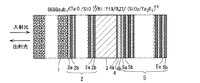
この光学体は、図1に示すように、SGGG(ガリウム・ガドリニウム・ガーネット基板)1の上へ、酸化タンタル2aと酸化シリコン2bとが交互に9層積層された第一の反射層2がブラッグミラーとして形成されている。そして、第一の反射層2の上には、ビスマス・イットリウム・ガーネットからなる磁気光学材料層3が形成されている。さらに、この磁気光学材料層3の上には透明性電極(ITO)4a、4bに両側から挟まれたPLZTからなる屈折率可変層5が積層されている。そして、さらに外側には酸化タンタル6aと酸化シリコン6bとが交互に18層積層された第二の反射層6がブラッグミラーとして形成されている。The inventors of the present invention have made extensive studies in order to solve such problems, and have focused on the device (optical body) disclosed in
This optical body can arbitrarily adjust the polarization angle of linearly polarized light, and is configured as follows.
As shown in FIG. 1, the optical body includes a first
このように構成された光学体では、直線偏光光であるレーザ光を入射光として第一の層1側から入射すると、ビスマス・イットリウム・ガーネットからなる磁気光学材料層3を通過して右回り円偏光光と左回りの円偏光光とに変換される。ここで右円偏光光と左円偏光光とには位相差がある。屈折率可変層5にかける電界を制御することにより、この位相差を変更できる。さらには、入射された光は第一の層1と第二の層6の間で多重反射させるため、当該位相差が増幅される。
In the optical body configured as described above, when laser light, which is linearly polarized light, is incident as incident light from the
したがって、磁気光学材料層3の磁気光学効果により生じた右円偏光光と左円偏光光との位相差が僅かなものであっても、第一の層1から出射する際には当該位相差は有意な大きさとなる。このように増幅された右円偏光光と左円偏光光との位相差は磁気光学材料層3を通過するときに直線偏光光に戻り、その偏光面の角度は当該位相差に応じて回転する。したがって、入射光に対して出射光は偏光面の回転角度が変調されたこととなる。
Therefore, even when the phase difference between the right circularly polarized light and the left circularly polarized light generated by the magneto-optical effect of the magneto-
ここにおいて、屈折率可変層5の屈折率を制御すれば、入射光に対する出射光の偏光面の回転角度変調を大きな範囲において、任意に制御可能となる。この光学体を用いて光変調システムを構築した場合、光の偏光状態を極めて速く制御することができる。このため、前述した光磁気書き込み方式のように、光の偏光状態の極めて速い変調を必要とする書き込み方式には適した光変調システムとなりうる。
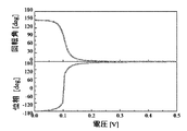
この光学体の特性(電圧−回転角特性)を図2及び図3(特許文献1の図11及び図9)に示す。Here, if the refractive index of the refractive
The characteristics (voltage-rotation angle characteristics) of this optical body are shown in FIGS. 2 and 3 (FIGS. 11 and 9 of Patent Document 1).
かかる光学体を詳細に検討した結果、以下の特性に気がついた。
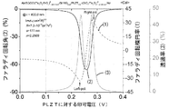
屈折率可変層へ印加する電圧を変化させると、回転角とともに回転楕円率(回転方向は一方向)も変化し、その変化に極大点(ピーク:絶対値の最大値)が存在した。このピークを生じる電圧に対応する回転角は小さいので、ピークを生じる電圧及びその前後の電圧の範囲は、直線偏光光の偏光面の回転角度を制御する際には一般的には使用しない。本発明者らは、かかる電圧の範囲を詳細に検討した結果、既述した回転楕円率にピークが存在することと、ゼロ電圧から当該ピークに対応する電圧まで屈折率可変層へ印加する電圧を掃引すると、回転楕円率がリニアに変化することに気がついた。なお、ゼロ電圧では回転楕円率はゼロであった。
かかる回転楕円率の特性(電圧−回転楕円率)において、回転楕円率はそのピークからゼロ電圧に対応する回転楕円率(=0)にかけてその絶対値が減少するので、この減少傾向をさらに進めれば、回転楕円率の符号が逆転するのではないかと考えた。
そこで、特許文献1に記載の光学体の層構成、特に回転角のピーク波長を変更してみた。具体的には、入射光の波長λ1に対して、回転角のピーク波長λ2(光学体内での共振波長)を僅かに大きくした。ちなみに、特許文献1に記載の光学体では入射光の波長λ1と回転角のピーク波長λ2とを一致させている。ピーク波長λ2の前後において回転角が大きく変化するからである。
入射光の波長λ1<回転角のピーク波長λ2としたときの特性を図5に示す。
なお、この特性はマトリックスアプローチ法に基づくシミュレートにより得た。このシミュレート計算については、M.Inoue,T.Fujii,"A theoretical analysis of magneto-optical Faraday effect of YIG films with random multilayer structure",Appl.Phys.81,317(1997).を参照されたい。そしてこの文献はこの明細書の一部として取り入れられる。
具体的な光学体の層構成については後述する。As a result of detailed examination of such an optical body, the following characteristics were noticed.
When the voltage applied to the refractive index variable layer was changed, the rotation ellipticity (rotation direction was one direction) also changed with the rotation angle, and there was a maximum point (peak: maximum absolute value) in the change. Since the rotation angle corresponding to the voltage causing the peak is small, the voltage causing the peak and the range of the voltages before and after the peak are generally not used when controlling the rotation angle of the polarization plane of the linearly polarized light. As a result of examining the range of such voltages in detail, the present inventors have found that there is a peak in the above-described rotational ellipticity, and the voltage applied to the refractive index variable layer from zero voltage to the voltage corresponding to the peak. I noticed that when I swept, the rotation ellipticity changed linearly. At zero voltage, the ellipticity of rotation was zero.
In such spheroid characteristics (voltage-rotational ellipticity), the absolute value of the rotational ellipticity decreases from the peak to the rotational ellipticity (= 0) corresponding to zero voltage, and this decreasing tendency can be further promoted. I thought that the sign of the rotation ellipticity might be reversed.
Therefore, the layer structure of the optical body described in
FIG. 5 shows the characteristics when the wavelength λ1 of the incident light is smaller than the peak wavelength λ2 of the rotation angle.
This characteristic was obtained by simulation based on the matrix approach. See M. Inoue, T. Fujii, “A theoretical analysis of magneto-optical Faraday effect of YIG films with random multilayer structure”, Appl. Phys. 81, 317 (1997). This document is then incorporated as part of this specification.
A specific layer structure of the optical body will be described later.
図5の結果から、電圧を変化させたとき、回転角のピークを境にして回転楕円率の符号が逆転することがわかる。即ち、回転の方向が逆転する。
更には、それぞれの符号においても(即ち、それぞれの回転方向においても)ピークが存在する。このピークを利用したとき、各回転方向の影響を記録媒体へ効率良く反映させられることはもとより、各ピークにおいて透過率も最大値を示しているので、高い出力を確保できる。From the results of FIG. 5, it can be seen that when the voltage is changed, the sign of the rotation ellipticity is reversed at the peak of the rotation angle. That is, the direction of rotation is reversed.
Furthermore, there is a peak in each code (that is, in each rotation direction). When this peak is used, the effect of each rotation direction can be efficiently reflected on the recording medium, and since the transmittance also shows the maximum value at each peak, a high output can be secured.
この発明は、本発明者らが見出した上記の知見に基づきなされたものであり、その第1の局面は次のように規定される。
第1の波長λ1の第1の光を放射する光源と、
前記第1の光を入射光とし、第2の波長λ2において偏光面の回転角度のピークを有し、第2の光を出力光として出力する光学体であって、一対の反射層、該一対の反射層の間に存在する屈折率可変層及び磁気光学材料層を有する光学体と、
前記屈折率可変層の屈折率を第1の屈折率と第2の屈折率とに制御しうる屈折率制御部と、を備えてなる光変調システムの制御方法であって、
前記光学体の回転角度のピークに対応する前記第2の波長λ2を前記入射光の波長λ1より大きくするとともに、
前記第1の屈折率では前記第2の光を第1の方向の楕円偏光光とし、前記第2の屈折率では前記第2の光を第2の方向の楕円偏光光とするように前記屈折率可変層の屈折率を制御する光変調システムの制御方法。The present invention has been made based on the above findings found by the present inventors, and the first aspect thereof is defined as follows.
A light source that emits first light of a first wavelength λ1,
An optical body that uses the first light as incident light, has a peak of the rotation angle of the polarization plane at the second wavelength λ2, and outputs the second light as output light. An optical body having a variable refractive index layer and a magneto-optical material layer present between the reflective layers of
A method of controlling a light modulation system comprising: a refractive index control unit capable of controlling a refractive index of the refractive index variable layer to a first refractive index and a second refractive index;
While making the second wavelength λ2 corresponding to the peak of the rotation angle of the optical body larger than the wavelength λ1 of the incident light,
In the first refractive index, the second light is elliptically polarized light in a first direction, and in the second refractive index, the second light is elliptically polarized light in a second direction. A method for controlling an optical modulation system for controlling a refractive index of a variable-index layer.
このように規定される第1の局面の光変調システムによれば、本発明者らが今回見出した新たな特性(図5参照)から明らかなように、電圧を調整して屈折率可変層の屈折率を第1の屈折率としたとき出力光(第2の光)を第1の方向の楕円偏光光とし、電圧を変化させて屈折率可変層の屈折率を第2の屈折率としたとき出力光(第2の光)を第1の方向と異なる符号の、即ち第1の方向と異なる回転方向(第2の回転方向)とすることができる。
屈折率可変層の屈折率の変更は電圧切換えで行えるので、出力光の回転方向を高速で切換えられる。According to the optical modulation system of the first aspect defined as described above, as is clear from the new characteristic found by the present inventors (see FIG. 5), the voltage is adjusted to adjust the refractive index variable layer. When the refractive index is the first refractive index, the output light (second light) is elliptically polarized light in the first direction, and the refractive index of the refractive index variable layer is changed to the second refractive index by changing the voltage. Sometimes, the output light (second light) may have a different sign from the first direction, that is, a rotation direction (second rotation direction) different from the first direction.
Since the refractive index of the refractive index variable layer can be changed by voltage switching, the rotation direction of the output light can be switched at high speed.
ここに、図5から明らかな通り、第1の方向と第2の方向においてそれぞれピーク(極大点)が存在するので、この両ピークの回転楕円率を利用できるように、光学体の回転角のピークに対応する波長λ2を定めることが好ましい。
勿論、回転楕円率のピーク値以外においても、異なる回転方向を得られる(回転楕円率の符号の異なる)領域を用いることにより、記録媒体にその違いを書き込むことができる。更には、回転楕円率がリニアに変化しているので、電圧(即ち屈折率)を適宜選択することにより、記憶媒体に対して2方向の回転に加えて、その中間値(濃淡)を書き込むこともできる。Here, as is apparent from FIG. 5, since there are peaks (maximum points) in the first direction and the second direction, the rotation angle of the optical body can be used so that the rotation ellipticity of both peaks can be used. It is preferable to define the wavelength λ2 corresponding to the peak.
Of course, the difference can be written on the recording medium by using regions where different rotation directions can be obtained (different signs of the rotation ellipticity) other than the peak value of the rotation ellipticity. Furthermore, since the rotation ellipticity changes linearly, by selecting the voltage (that is, the refractive index) as appropriate, in addition to the rotation in two directions, the intermediate value (light / dark) is written to the storage medium. You can also.
図5に示された特性より、電圧の変化に伴い、回転角度と回転楕円率とがともに変化していることを新たに見出した。更に詳細にいえば、回転楕円率がゼロからそのピークの電圧範囲において、回転楕円率と回転角度がともにリニアに変化している。
かかる特性の存在は、特許文献1に記載の光学体へ一般的な使用範囲(回転角度がゼロ近くまで)を超えて電圧を掃引してはじめて知り得るものである。この特性は、光学体の回転角度のピークに対応した波長λ2と入力光の波長λ1とを等しくしたときにも得られる。
以上の知見に基づき、この発明の他の第2の局面は次のように規定される。
一対の反射層、該一対の反射層の間に存在する屈折率可変層及び磁気光学材料層を有する光学体を備える光変調部と、
前記屈折率可変層の屈折率を第1の屈折率と第2の屈折率に制御しうる屈折率制御部と、を備えてなる光変調システムの制御方法であって、
前記第2の光の偏光面の回転角度と楕円率とをともに変化させるように屈折率可変層の屈折率を制御する光変調システムの制御方法。
この光変調システムの制御方法では、屈折率可変層の屈折率を変化させることにより、第2の光の偏光面の回転角度と楕円率とをともに変化させられる。From the characteristics shown in FIG. 5, it was newly found that both the rotation angle and the rotation ellipticity change with the change of voltage. More specifically, both the rotation ellipticity and the rotation angle change linearly in the voltage range from zero to its peak.
The existence of such characteristics can be known only after the voltage is swept beyond the general use range (up to a rotation angle close to zero) in the optical body described in
Based on the above knowledge, another second aspect of the present invention is defined as follows.
A light modulator comprising an optical body having a pair of reflective layers, a refractive index variable layer and a magneto-optical material layer existing between the pair of reflective layers;
A method of controlling an optical modulation system comprising: a refractive index control unit capable of controlling a refractive index of the refractive index variable layer to a first refractive index and a second refractive index;
A control method of a light modulation system for controlling a refractive index of a refractive index variable layer so as to change both a rotation angle and an ellipticity of a polarization plane of the second light.
In this light modulation system control method, both the rotation angle and ellipticity of the polarization plane of the second light can be changed by changing the refractive index of the refractive index variable layer.
なお、特許文献1に記載の光学体では、直線偏光光である入射光に対して出力光も直線偏光光としてその偏光面の回転角度を制御していた。この発明の光学体も基本的な層構成は特許文献1に記載の光学体のそれと同一であるが、一対の反射層の反射率を調整することにより、入射光の入射面と反対側の面より円偏光された出力光を取り出せるようにしている。
In the optical body described in
以下、本発明の光変調システムについて詳細に説明する。
この光変調システムは、図4に示すように、光学体10、光源20及び屈折率制御部30を備えてなる。
光学体10は基板11上に、第一の反射層12、磁気光学材料層13、透光性電極14a、14bに挟持された屈折率可変層14及び第二の反射層15を順次積層した構成である。
基板11の材質は任意に選択可能であるが、従来例(図1参照)と同様にSGGGを採用可能である。
第一の反射層12及び第二の反射層15にはともに誘電体多層膜からなるブラッグミラー層や金属膜を採用することができる。
反射層としてブラックミラー層を採用する場合、誘電体多層膜の繰り返し単位を構成する誘電体層のペアの材質及び膜厚はブラッグの反射条件(d=λ/4:ここに、λは各層の光学波長、dは各層の膜厚)を満足することを条件に、入射光の波長や用途に応じて任意に選択できる。具体的には、誘電体層のペアとして酸化シリコン(SiO2)と酸化タンタル(Ta2O5)との組合せ、酸化シリコン(SiO2)とシリコン(Si)、酸化シリコン(SiO2)と酸化アルミニウム(Al2O3)等が挙げられる。Hereinafter, the light modulation system of the present invention will be described in detail.
As shown in FIG. 4, the light modulation system includes an
The
Although the material of the board | substrate 11 can be selected arbitrarily, SGGG is employable similarly to a prior art example (refer FIG. 1).
Both the first
When a black mirror layer is employed as the reflection layer, the material and film thickness of the dielectric layer pair constituting the repeating unit of the dielectric multilayer film are Bragg reflection conditions (d = λ / 4: where λ is the value of each layer The optical wavelength, d can be arbitrarily selected according to the wavelength of the incident light and the application, provided that the film thickness satisfies the condition (d is the film thickness of each layer). Specifically, a combination of silicon oxide (SiO 2 ) and tantalum oxide (Ta 2 O 5 ) as a pair of dielectric layers, silicon oxide (SiO 2 ) and silicon (Si), silicon oxide (SiO 2 ) and oxide aluminum (Al 2 O 3), and the like.
誘電体層ペアの繰返し数も任意に選択可能であるが、第一の反射層と第二の反射層とで同じ誘電体ペアを採用するときは、第一の反射層の繰返し数より第二の反射層の繰返し数が大きいものとする。誘電体層のペアとして酸化シリコン(SiO2) と酸化タンタル(Ta2O5)との組合せを採用したときは、第一の反射層は3ペア以上、第二の反射層は5ペア以上とすることが好ましい。更に好ましくは、第一の反射層は5ペア以上、第二の反射層は7ペア以上とする。
また金属層としては、アルミニウム、白金、金、銀及びこれらの合金の単層膜若しくは複層膜を挙げることができる。The number of repetitions of the dielectric layer pair can be arbitrarily selected. However, when the same dielectric pair is adopted for the first reflection layer and the second reflection layer, the second number of repetitions is determined by the number of repetitions of the first reflection layer. It is assumed that the number of repetitions of the reflective layer is large. When a combination of silicon oxide (SiO 2 ) and tantalum oxide (Ta 2 O 5 ) is adopted as a pair of dielectric layers, the first reflective layer is 3 pairs or more, and the second reflective layer is 5 pairs or more. It is preferable to do. More preferably, the first reflective layer is 5 pairs or more, and the second reflective layer is 7 pairs or more.
Examples of the metal layer include a single layer film or a multilayer film of aluminum, platinum, gold, silver, and alloys thereof.
この光学体では入射光を第一の反射層12へ入射し、第二の反射層15側から透過した光を出力光としている。この出力光は楕円偏光光となる。
In this optical body, incident light is incident on the first
第一の層と第二の層との間隔は、m×λ/2(ここに、mは自然数、λは第一の層と第二の層との間の光学波長)とする。これにより、第一の層と第二の層との間隔が光学波長の節の幅と一致する。
ここに光学波長はλ0/nで規定される。λ0は真空における入射光の波長、nは実効屈折率である。第一の層と第二の層との間に1種類の材料層のみが介在されるとき、実効屈折率nは当該材料の屈折率に等しい。第一の層と第二の層との間に複数の材料層が介在するときは、複数の異なる材料が連続する層を1つの材料の1つの層と見なしたときの屈折率である。例えば、連続する2層の片方の屈折率と膜厚をn1、d1とし、もう片方をn2、d2としたとき、(n1×d1+n2×d2)/(d1+n2)が連続する2層の実効屈折率となる。The distance between the first layer and the second layer is m × λ / 2 (where m is a natural number and λ is an optical wavelength between the first layer and the second layer). Thereby, the space | interval of a 1st layer and a 2nd layer corresponds with the width | variety of the node of an optical wavelength.
Here, the optical wavelength is defined by λ 0 / n. λ 0 is the wavelength of incident light in vacuum, and n is the effective refractive index. When only one kind of material layer is interposed between the first layer and the second layer, the effective refractive index n is equal to the refractive index of the material. When a plurality of material layers are interposed between the first layer and the second layer, the refractive index is obtained when a layer in which a plurality of different materials are continuous is regarded as one layer of one material. For example, when the refractive index and film thickness of one of two consecutive layers are n 1 and d 1 and the other is n 2 and d 2 , (n 1 × d 1 + n 2 × d 2 ) / (d 1 + N 2 ) is an effective refractive index of two consecutive layers.
設計容易性の観点からは、第一の層と第二の層の間に複数の層が介在される場合は、各層の厚さを(各層の光学波長/2)の自然数倍とすることが好ましい。例えば、第一の層と第二の層との間に層A及び層Bが介在される場合、層A及び層Bの厚さをそれぞれ(m1×λA)/2、(m2×λB)/2とする。ここに、λAは層Aの光学波長、λBは層Bの光学波長である。このように設計すれば、第一の層と第二の層との間に複数の層が介在される場合においても、第一の層と第二の層との間隔はm×λ/2(ここに、mは自然数、λは第一の層と第二の層間の光学波長)の関係が常に維持される。第一の層と第二の層との間に透光性電極層を介在させる場合には、当該透光性電極層も上記の関係を保持するものとすることが好ましい。From the viewpoint of ease of design, when a plurality of layers are interposed between the first layer and the second layer, the thickness of each layer should be a natural number times (optical wavelength / 2 of each layer). Is preferred. For example, when the layer A and the layer B are interposed between the first layer and the second layer, the thicknesses of the layer A and the layer B are (m 1 × λ A ) / 2, (m 2 × λ B ) / 2. Here, λ A is the optical wavelength of layer A, and λ B is the optical wavelength of layer B. With this design, even when a plurality of layers are interposed between the first layer and the second layer, the distance between the first layer and the second layer is m × λ / 2 ( Here, m is a natural number, and λ is an optical wavelength between the first layer and the second layer). When a translucent electrode layer is interposed between the first layer and the second layer, it is preferable that the translucent electrode layer also maintains the above relationship.
上記において、第一の層と第二の層との間隔を規定するとき、及び第一の層と第二の層との間に介在される複数の層における各層の厚さを規定するときに光学波長λが用いられている。この光学波長λは多少のマージンを有することができる。各層の厚さをnmオーダーで正確に制御することは極めて困難だからである。また、多少のマージン(好ましくは±10%以内、更に好ましくは±5%以内)があっても、目的にかなった変調ができるからである。
第一の層及び第二の層は反射層とすることが好ましいことは既述したが、第一の層及び第二の層の少なくとも一方を誘電体多重層(ブラッグミラー層)としたとき、多重層を構成する誘電体層の一部又は全部を磁気光学材料や電気光学材料などの屈折率可変層で形成すると、これらの層も光の変調機能に寄与する場合がある。In the above, when defining the distance between the first layer and the second layer, and when defining the thickness of each layer in the plurality of layers interposed between the first layer and the second layer An optical wavelength λ is used. This optical wavelength λ can have some margin. This is because it is extremely difficult to accurately control the thickness of each layer on the order of nm. Further, even if there is a slight margin (preferably within ± 10%, more preferably within ± 5%), modulation suitable for the purpose can be performed.
As described above, the first layer and the second layer are preferably reflective layers, but when at least one of the first layer and the second layer is a dielectric multilayer (Bragg mirror layer), When some or all of the dielectric layers constituting the multilayer are formed of a refractive index variable layer such as a magneto-optic material or an electro-optic material, these layers may also contribute to the light modulation function.
磁気光学材料層13を構成する磁気光学材料は磁気光学効果(ファラディ効果、カー効果)を有し、直線偏光光が磁気光学材料の中を通ると、これを右回りの楕円偏光光(右円偏光光)と左回りの楕円偏光光(左円偏光光)とに変換する。このとき、右円偏光光と左円偏光光とには位相差が生じている。またこの磁気光学材料は非相反性を有するので、位相差の生じた右円偏光光と左円偏光光を再度磁気光学材料へ通過させて直線偏光光へ再変換したとき、その位相差が維持されて直線偏光光の偏光面の回転(角度の変化)としてあらわれる。
The magneto-optic material constituting the magneto-
このような磁気光学効果を奏する磁気光学材料には強磁性体材料、反強磁性体材料、フェリ磁性体材料、常磁性体材料を挙げられる。ファラディ効果を奏する透光性の強磁性体材料としてCdCo、のような磁性記憶媒体用材料、CoFe2O4のようなスピネルフェライト、PbFe12O19のようなヘキサゴナルフェライト、CdCr2S4のようなカルコゲナイド、フェライト、CrCl3のようなクロム化トリハライド、Y3Fe5O12(BiY)3Fe5O12のようなガーネット、(LaSr)MoO3のようマンガン酸化合物、EuOのようなユウロピウム化合物、Fe及びその合金からなる金属薄膜、Co及びその合金からなる薄膜、Mn及びその合金からなる薄膜、その他Fe2O4等やポリエチレン等の有機材料を挙げることができる。Examples of the magneto-optical material exhibiting such a magneto-optical effect include a ferromagnetic material, an antiferromagnetic material, a ferrimagnetic material, and a paramagnetic material. As a translucent ferromagnetic material exhibiting a Faraday effect, materials for magnetic storage media such as CdCo, spinel ferrite such as CoFe 2 O 4 , hexagonal ferrite such as PbFe 12 O 19 , and CdCr 2 S 4 Chalcogenides, ferrites, chromated trihalides such as CrCl 3 , garnets such as Y 3 Fe 5 O 12 (BiY) 3 Fe 5 O 12 , manganic acid compounds such as (LaSr) MoO 3 , europium compounds such as EuO And a metal thin film made of Fe and its alloy, a thin film made of Co and its alloy, a thin film made of Mn and its alloy, and other organic materials such as Fe 2 O 4 and polyethylene.
ファラディ効果を奏する透光性の反強磁性体材料としては、酸化マンガン等を挙げることができる。 Examples of the light-transmitting antiferromagnetic material that exhibits the Faraday effect include manganese oxide.
常磁性体材料は外部から磁界を印加することにより磁気光学効果を奏する。
ファラディ効果を奏する透光性の常磁性体材料として、Tb3AlO12、GGG(Gd3Ga5O12)等の希土類Al置換ガーネット、酸素等の気体、水等の液体、塩化カリウム等の固体、GGG(Gd3Ga5O12)、GGS等のクラウン等のガラスを挙げることができる。
青色光のような短波長を変調対象とする際には、TAG、TGGを採用することが好ましい。短波長をほとんど吸収しないからである。
磁性体材料層は単層若しくは複数層とすることができる。複数層とした場合、この複数層を構成する各層は同一の材料であっても異なる材料であってもよい。Paramagnetic materials exhibit a magneto-optical effect by applying a magnetic field from the outside.
As a translucent paramagnetic material exhibiting a Faraday effect, rare earth Al-substituted garnet such as Tb 3 AlO 12 , GGG (Gd 3 Ga 5 O 12 ), gas such as oxygen, liquid such as water, solid such as potassium chloride , GGG (Gd 3 Ga 5 O 12 ), GGS and other glasses.
When a short wavelength such as blue light is to be modulated, it is preferable to employ TAG and TGG. This is because the short wavelength is hardly absorbed.
The magnetic material layer can be a single layer or a plurality of layers. In the case of a plurality of layers, the layers constituting the plurality of layers may be the same material or different materials.
屈折率可変層14はこれを通過する光に対して、光通過方向にその屈折率を変化させる。
かかる屈折率可変層14を形成する材料として電気光学材料、音響光学材料、熟光学材料等を挙げることができる。電気光学材料は電界の印加によって屈折率が変化する材料であって、PZT(PbZr0.25Ti0.48O3)、PLZT、PLHT、SBN、LT、LN、KDP、DKDP、BNN、KTN、BTO等を挙げることができる。
屈折率可変層14を電気光学材料で形成した場合、当該屈折率可変層へ印加する電界を制御することにより、その屈折率を変化・制御可能である。屈折率可変層へ電界を印加するために、特許文献1にも記載してある通り、当該屈折率可変層を透光性電極14a、14bでサンドイッチする構成を採用できる。勿論、光学体の外部から電界を印加してもよい。この場合、電界の印加の方向は屈折率可変層の面内方向に対して垂直に限らず、傾斜していてもよい。The refractive
Examples of a material for forming the refractive
When the refractive
音響光学材料は応力の印加・歪によって屈折率変化が生じる材料であって、PZT (PbZr0.25Ti0.48O3)、LT、LN、Al2O3、Y3Al5O12、Si、SiO2等を挙げることができる。
屈折率可変層14を音響光学材料で形成した場合、当該屈折率可変層14へ印加する応力を制御することにより、その屈折率を変化させることにより制御可能である。屈折率可変層14へ応力を印加するためには、屈折率可変層を光透過性の圧電素子で挟むことが考えられる。The acousto-optic material is a material in which the refractive index changes due to the application of stress and strain. PZT (PbZr 0.25 Ti 0.48 O 3 ), LT, LN, Al 2 O 3 , Y 3 Al 5 O 12 , Si, SiO 2 Etc.
When the refractive
熱光学材料は温度により屈折率が変化する材料であって、液晶が該当する屈折率可変層を熱光学材料で形成した場合、当該屈折率可変層へ印加する熱を制御することにより、その屈折率を変化させることにより制御可能である。屈折率可変層の温度を制御するには、例えばヒーターを具備すればよい A thermo-optic material is a material whose refractive index changes with temperature. When a refractive index variable layer corresponding to liquid crystal is formed of a thermo-optic material, the refractive index is controlled by controlling the heat applied to the variable refractive index layer. It can be controlled by changing the rate. In order to control the temperature of the refractive index variable layer, for example, a heater may be provided.
屈折率可変層14は単層若しくは複数層とすることができる。複数層とした場合、この複数層を構成する各層は同一の材料であっても異なる材料であってもよい。
The refractive
この明細書において「透光性」とは入射光(変調対象光)を透過する特性を指し、いわゆる透明性(可視光についての透光性)に限られるものではない。また、屈折率可変層は必然的に透光性を有するものとする。
カー効果を有する材料としてはR3Fe5O12 (R-希土類元素、例えばBi、Y、Sm、Eu、Gd、Tb、Dy、Ho、Er、Tm、Yb、Lu)のようなガーネット、MFe2O4(M=Mn、Fe、Co、Ni、Cu、Mg、Li0.5Fe0.5)のようなスピネルフェライト、MFe2O4(M=Ba、Pb、Sr、Ca、Ni0.5Fe0.5、Ag0.5La0.5)のような六方晶フェライト、MnBi、PtCo、EuO、PtMnSbからなる多結晶膜、Gd-Co、Gd-Fe、Dy-Fe、Tb-Fe、Gd-Tb-Fe、Gd-Dy-Fe、Tb-Fe-Co、Gd-Tb-Fe-Co、(Gd-Fe)-Bi、(Gd-Fe)-Sn、Nd-Dy-Fe-Coのような希土類一遷移金属薄膜、及び前記材料からなる薄膜からなる複合膜等を挙げることができる。In this specification, “translucency” refers to a characteristic of transmitting incident light (modulation target light) and is not limited to so-called transparency (translucency for visible light). In addition, the refractive index variable layer necessarily has translucency.
Materials having a Kerr effect include R 3 Fe 5 O 12 (R-rare earth elements such as Bi, Y, Sm, Eu, Gd, Tb, Dy, Ho, Er, Tm, Yb, Lu), MFe Spinel ferrite such as 2 O 4 (M = Mn, Fe, Co, Ni, Cu, Mg, Li 0.5 Fe 0.5 ), MFe 2 O 4 (M = Ba, Pb, Sr, Ca, Ni 0.5 Fe 0.5 , Ag Hexagonal ferrite such as 0.5 La 0.5 ), polycrystalline film composed of MnBi, PtCo, EuO, PtMnSb, Gd-Co, Gd-Fe, Dy-Fe, Tb-Fe, Gd-Tb-Fe, Gd-Dy- Rare earth single transition metal thin films such as Fe, Tb-Fe-Co, Gd-Tb-Fe-Co, (Gd-Fe) -Bi, (Gd-Fe) -Sn, Nd-Dy-Fe-Co, and A composite film made of a thin film made of a material can be mentioned.
磁気光学材料層を光透過性としたとき、磁気光学材料層と屈折率可変層との積層体を繰返してなる多層構造を採用することもできる。この多層構造を採用する場合、各磁気光学材料層は同一の材料で形成することが好ましいが、また異なる材料で形成することを除外するものではない。同様に、各屈折率可変層も同一の材料で形成することが好ましいが、異なる材料で形成してもよい。 When the magneto-optical material layer is made light transmissive, a multilayer structure in which a laminate of the magneto-optical material layer and the refractive index variable layer is repeated can also be adopted. When this multilayer structure is adopted, each magneto-optic material layer is preferably formed of the same material, but it is not excluded to form it with different materials. Similarly, each refractive index variable layer is preferably formed of the same material, but may be formed of different materials.
光源20は直線偏光光を出力可能とし、例えば半導体レーザ装置を用いることができる。光源から出力される入射光の波長をλ1とする。
ここに、光学体10はその回転角度のピーク波長をλ2としたとき、λ1<λ2とする。これにより、屈折率可変層14の屈折率を変化させたとき、出力される楕円偏光光の回転楕円率の符号を逆転可能とし、かつ各回転方向においてピーク値を得ることができる。
なお、回転角度のピーク波長とは、光学体において入力光を、最も効率よく角度偏光できる波長をさす。
光学体においてピーク波長の制御は、磁気光学材料層の材質及び/又は厚さ等を制御することにより行なえる。
以下に説明する実施例では、入射光の波長λ1=800.0nm、光学体における回転角度のピーク波長λ2=800.5nmとした。The
Here, when the peak wavelength of the rotation angle of the
The peak wavelength of the rotation angle refers to a wavelength at which the input light can be angularly polarized most efficiently in the optical body.
In the optical body, the peak wavelength can be controlled by controlling the material and / or thickness of the magneto-optical material layer.
In the examples described below, the wavelength λ1 of incident light is 800.0 nm, and the peak wavelength λ2 of the rotation angle in the optical body is 800.5 nm.
屈折率制御部30は屈折率可変層14の屈折率を変更するものであり、屈折率可変層14の特性に応じて屈折率可変層14へ所望のエネルギーを印加する。
屈折率可変層14を電気光学材料で形成し、そこへ電界を印加することによりその屈折率を制御する方式が、屈折率切換えを高速にかつ簡易な構成で実行できるので好ましい。より具体的には、電気光学材料からなる屈折率可変層を一対の透光性電極で挟み、一対の透光性電極へ印加する電圧を切換えることにより、簡易かつ高速に屈折率可変層の屈折率を任意に制御可能となる。The refractive
A method in which the refractive
以下、この発明の実施例の光変調システムを、図4を参照しながら、説明する。 An optical modulation system according to an embodiment of the present invention will be described below with reference to FIG.
<半導体レーザ装置>
半導体レーザ装置20は、800nmのレーザ光を放射可能とされている。<Semiconductor laser device>
The
<光学体>
また、光学体10は、SGGG(ガリウム・ガドリニウム・ガーネット基板:例えばGd2.68Ca0.32Ga4.04Mg0.32Zr0.64O12)11の上へ、酸化タンタル12aと酸化シリコン12bとが交互に9層積層された第一の反射層12がブラッグミラーとして形成されている。そして、第一の反射層12の上には、ビスマス・イットリウム・ガーネットからなる磁気光学材料層13が形成されている。さらに、この磁気光学材料層13の上には透明性電極(ITO)14a、14bに両側から挟まれたPLZTからなる屈折率可変層14が積層されている。そして、さらに外側には酸化タンタル15aと酸化シリコン15bとが交互に9層積層された第二の反射層15がブラッグミラーとして形成されている。<Optical body>
The
各層の厚さは以下のとおりである。
第一の反射層12:光学長λ=800.5nm
(酸化タンタル12aと酸化シリコン12bとの合計の厚さ)
第二の反射層15:光学長λ=800.5nm
(酸化タンタル15aと酸化シリコン15bとの合計の厚さ)
磁気光学材料層13(ビスマス・イットリウム・ガーネット):m=4
ここでmは自然数(1,2,3……)である。
屈折率可変層15(PLZT):m=1
ここでmは自然数(1,2,3……)である。
透明性電極(ITO)14a、14b:
後述するシミュレーションにおいて、透光性電極は厚さを持たず、かつその材料は完全な透光性であり、かつ電気抵抗を持たないものと仮定している。The thickness of each layer is as follows.
First reflective layer 12: optical length λ = 800.5 nm
(Total thickness of tantalum oxide 12a and silicon oxide 12b)
Second reflective layer 15: optical length λ = 800.5 nm
(Total thickness of tantalum oxide 15a and silicon oxide 15b)
Magneto-optic material layer 13 (bismuth / yttrium / garnet): m = 4
Here, m is a natural number (1, 2, 3,...).
Refractive index variable layer 15 (PLZT): m = 1
Here, m is a natural number (1, 2, 3,...).
Transparent electrodes (ITO) 14a, 14b:
In the simulation described later, it is assumed that the translucent electrode does not have a thickness, and the material is completely translucent and does not have an electrical resistance.
これらの各層はスパッタリング法によって形成することができる。ただし、スパッタリング法に限定されるものではなく、蒸着法、イオンプレーティング法、スプレー法、イオンビーム照射法などのPVD法や、CVD法など、汎用的な薄膜製造技術を適用可能である。 Each of these layers can be formed by sputtering. However, the method is not limited to the sputtering method, and general-purpose thin film manufacturing techniques such as a PVD method such as an evaporation method, an ion plating method, a spray method, and an ion beam irradiation method, and a CVD method can be applied.
<屈折率制御部>
屈折率制御部30は、透明性電極(ITO)14a、4b間に所定の電位を付与することが可能な電源を備え、透明性電極(ITO)14a、14bに接続されている。屈折率制御部30による付与制御内容については、後述するシミュレーション計算の項において説明する。<Refractive index control unit>
The refractive
以上のように構成された光変調システムについて、半導体レーザ装置20を用いて直線偏光光であるレーザ光を入射光として第一の層11側から入射した場合のシミュレート計算をマトリックスアプローチ法によって行った。シミュレート計算は、透過光および反射光の両方について行った。
With respect to the light modulation system configured as described above, a simulation calculation is performed by the matrix approach method when the laser beam, which is linearly polarized light, is incident as incident light from the first layer 11 side using the
<透過光の場合>
透過光の場合のシミュレート計算の結果を図5及び図6に示す。
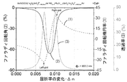
図5はPLZTからなる屈折率可変層14への印加電圧と、ファラディ回転角、ファラディ回転楕円率及び透過率との関係を示すグラフである。このグラフから、印加電圧が0.26V付近にファラディ回転角のピークが存在し、さらにそのピークを中心に少しずれた両外側に、正負を逆とするファラディ回転楕円率のピークが存在することが分かった。また、ファラディ回転楕円率のピークと透過率の最大ピークの位置とは一致することが分かった。<For transmitted light>
The result of the simulation calculation in the case of transmitted light is shown in FIGS.
FIG. 5 is a graph showing the relationship between the voltage applied to the refractive
一方、図6は透過光における屈折率可変層15の屈折率の変化Δnと、ファラディ回転角、ファラディ回転楕円率及び透過率との関係を示すグラフである。このグラフから、屈折率の変化Δnが0.0075付近にファラディ回転角のピークが存在し、さらにそのピークを中心に少しずれた両外側に、正負を逆とするファラディ回転楕円率のピークが存在することが分かった。また、ファラディ回転楕円率のピークと透過率の最大ピークの位置とは一致することが分かった。
On the other hand, FIG. 6 is a graph showing the relationship between the refractive index change Δn of the refractive
<反射光の場合>
反射光の場合のシミュレート計算の結果を図7及び図8に示す。
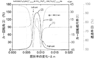
図7は透過光における屈折率の変化と、カー回転角、カー回転楕円率及び透過率との関係を示すグラフである。
透過光における屈折率可変層15の屈折率の変化と、カー回転角、カー回転楕円率及び透過率との関係を示すグラフである。このグラフから、印加電圧が0.26V付近にカー回転角のピークが存在しており、さらにそのピークを中心に少しずれた両外側に、正負を逆とするカー回転楕円率のピークが存在することが分かった。また、カー回転楕円率のピークと透過率の最大ピークの位置とは一致することが分かった。
一方、図8は屈折率の変化(Δn)と、カー回転角、カー回転楕円率及び透過率との関係を示すグラフである。このグラフから、屈折率の変化Δnが0.0075付近にカー回転角のピークが存在し、さらにそのピークを中心に少しずれた両外側に、正負を逆とするカー回転楕円率のピークが存在することが分かった。また、カー回転楕円率のピークと透過率の最大ピークの位置とは一致することが分かった。<In the case of reflected light>
The result of the simulation calculation in the case of reflected light is shown in FIGS.
FIG. 7 is a graph showing the relationship between the change in refractive index of transmitted light and the Kerr rotation angle, Kerr rotation ellipticity, and transmittance.
It is a graph which shows the relationship between the change of the refractive index of the refractive
On the other hand, FIG. 8 is a graph showing the relationship between the refractive index change (Δn) and the Kerr rotation angle, Kerr rotation ellipticity, and transmittance. From this graph, there is a Kerr rotation angle peak near a refractive index change Δn of around 0.0075, and there are Kerr rotation ellipticity peaks that are opposite to each other on both sides slightly shifted from the peak. I found out that It was also found that the Kerr rotation ellipticity peak coincides with the position of the maximum transmittance peak.
この例では、入射光として波長λ1=800.0nmのレーザ光を用い、光学体におけるピーク波長をλ2=800.5nmに設定している。 In this example, laser light having a wavelength λ1 = 800.0 nm is used as incident light, and the peak wavelength in the optical body is set to λ2 = 800.5 nm.
以上のように、実施例1の光変調システムでは、屈折率可変層14への印加電圧を制御することにより、レーザ光の透過光や反射光において、正負を逆とする回転楕円率のピークが存在するという特異な効果を奏することができる。
このため、書き込み時に使用する光が右円偏光か左円偏光かによって磁化の反転を制御する記録媒体の書き込み用の光源として用いることができる。また、印加電圧の変化は、屈折率可変層に付与される電界変化となって現れ、屈折率の高速制御が可能となるため、高速書き込みが可能となる。As described above, in the light modulation system according to the first embodiment, by controlling the voltage applied to the refractive
For this reason, it can be used as a light source for writing in a recording medium that controls the reversal of magnetization depending on whether the light used for writing is right circularly polarized light or left circularly polarized light. In addition, the change in the applied voltage appears as a change in the electric field applied to the refractive index variable layer, and the refractive index can be controlled at high speed, so that high-speed writing is possible.
12、15…反射層(12…第一の反射層、15…第二の反射層)
10、20…光変調部(10…光学体、20…半導体レーザ装置(光源))
14…屈折率可変層
13…磁気光学材料層
14a、14b、30…屈折率制御部(14a、14b…透明性電極、30…電位発生装置)
12, 15 ... reflective layer (12 ... first reflective layer, 15 ... second reflective layer)
10, 20... Light modulator (10... Optical body, 20... Semiconductor laser device (light source))
DESCRIPTION OF
Claims (9)
前記第1の光を入射光とし、第2の波長λ2において回転角度のピークを有し、第2の光を出力光として出力する光学体であって、一対の反射層、該一対の反射層の間に存在する屈折率可変層及び磁気光学材料層を有する光学体と、
前記屈折率可変層の屈折率を第1の屈折率と第2の屈折率とに制御しうる屈折率制御部と、を備えてなる光変調システムの制御方法であって、
前記光学体の回転角度のピークに対応する前記第2の波長λ2を前記入射光の波長λ1より大きくするとともに、
前記第1の屈折率では前記第2の光を第1の方向の楕円偏光光とし、前記第2の屈折率では前記第2の光を第2の方向の楕円偏光光とするように前記屈折率可変層の屈折率を制御する光変調システムの制御方法。 A light source that emits first light of a first wavelength λ1,
An optical body that uses the first light as incident light, has a rotation angle peak at the second wavelength λ2, and outputs the second light as output light, comprising a pair of reflective layers and the pair of reflective layers An optical body having a refractive index variable layer and a magneto-optical material layer existing between
A method of controlling a light modulation system comprising: a refractive index control unit capable of controlling a refractive index of the refractive index variable layer to a first refractive index and a second refractive index;
While making the second wavelength λ2 corresponding to the peak of the rotation angle of the optical body larger than the wavelength λ1 of the incident light,
In the first refractive index, the second light is elliptically polarized light in a first direction, and in the second refractive index, the second light is elliptically polarized light in a second direction. A method for controlling an optical modulation system for controlling a refractive index of a variable-index layer.
前記屈折率可変層の屈折率を第1の屈折率と第2の屈折率に制御しうる屈折率制御部と、を備え
直線偏光光を入力して楕円偏光光を出力する、光変調システムの制御方法であって、
前記楕円偏光光の回転角度と回転楕円率とをともに変化させるように屈折率可変層の屈折率を制御する光変調システムの制御方法。 An optical body having a pair of reflective layers, a refractive index variable layer and a magneto-optical material layer present between the pair of reflective layers;
A refractive index control unit capable of controlling a refractive index of the refractive index variable layer to a first refractive index and a second refractive index, wherein linearly polarized light is input and elliptically polarized light is output. A control method,
A method for controlling a light modulation system, wherein the refractive index of the refractive index variable layer is controlled so as to change both the rotation angle and the rotation ellipticity of the elliptically polarized light.
前記第1の光を入射光とし、第2の波長λ2において回転角度のピークを有し、第2の光を出力光として出力する光学体であって、一対の反射層、該一対の反射層の間に存在する屈折率可変層及び磁気光学材料層を有する光学体と、
前記屈折率可変層の屈折率を第1の屈折率と第2の屈折率とに制御しうる屈折率制御部と、
前記第1の屈折率では前記第2の光を第1の方向の楕円偏光光とし、前記第2の屈折率では前記第2の光を第2の方向の楕円偏光光とするように前記屈折率可変層の屈折率を制御する制御部と、を備え、
前記光学体の回転角度のピークに対応する前記第2の波長λ2が前記入射光の波長λ1より大きい、光変調システム。 A light source that emits first light of a first wavelength λ1,
An optical body that uses the first light as incident light, has a rotation angle peak at the second wavelength λ2, and outputs the second light as output light, comprising a pair of reflective layers and the pair of reflective layers An optical body having a refractive index variable layer and a magneto-optical material layer existing between
A refractive index control unit capable of controlling a refractive index of the refractive index variable layer to a first refractive index and a second refractive index;
In the first refractive index, the second light is elliptically polarized light in a first direction, and in the second refractive index, the second light is elliptically polarized light in a second direction. A control unit for controlling the refractive index of the variable rate layer,
The light modulation system, wherein the second wavelength λ2 corresponding to the rotation angle peak of the optical body is larger than the wavelength λ1 of the incident light.
The system according to claim 8, wherein the refractive index control unit includes a pair of transparent electrodes sandwiching the refractive index variable layer.
Priority Applications (1)
| Application Number | Priority Date | Filing Date | Title |
|---|---|---|---|
| JP2013521600A JP6108398B2 (en) | 2011-06-20 | 2012-06-20 | Light modulation system control method, light modulation system, and optical body used therefor |
Applications Claiming Priority (4)
| Application Number | Priority Date | Filing Date | Title |
|---|---|---|---|
| JP2011136586 | 2011-06-20 | ||
| JP2011136586 | 2011-06-20 | ||
| PCT/JP2012/065753 WO2012176807A1 (en) | 2011-06-20 | 2012-06-20 | Method for controlling optical modulation system, optical modulation system and optical body used therein |
| JP2013521600A JP6108398B2 (en) | 2011-06-20 | 2012-06-20 | Light modulation system control method, light modulation system, and optical body used therefor |
Publications (2)
| Publication Number | Publication Date |
|---|---|
| JPWO2012176807A1 JPWO2012176807A1 (en) | 2015-02-23 |
| JP6108398B2 true JP6108398B2 (en) | 2017-04-05 |
Family
ID=47422639
Family Applications (1)
| Application Number | Title | Priority Date | Filing Date |
|---|---|---|---|
| JP2013521600A Expired - Fee Related JP6108398B2 (en) | 2011-06-20 | 2012-06-20 | Light modulation system control method, light modulation system, and optical body used therefor |
Country Status (2)
| Country | Link |
|---|---|
| JP (1) | JP6108398B2 (en) |
| WO (1) | WO2012176807A1 (en) |
Families Citing this family (1)
| Publication number | Priority date | Publication date | Assignee | Title |
|---|---|---|---|---|
| JP6172652B2 (en) * | 2013-02-20 | 2017-08-02 | 国立大学法人豊橋技術科学大学 | Magnetophotonic crystal, magneto-optical imaging apparatus, magneto-optical recording medium, arithmetic element |
Family Cites Families (2)
| Publication number | Priority date | Publication date | Assignee | Title |
|---|---|---|---|---|
| JP5061876B2 (en) * | 2007-12-12 | 2012-10-31 | 株式会社村田製作所 | Bandpass filter |
| EP2487525B1 (en) * | 2009-10-07 | 2019-09-18 | National University Corporation Toyohashi University of Technology | Optical body |
-
2012
- 2012-06-20 WO PCT/JP2012/065753 patent/WO2012176807A1/en active Application Filing
- 2012-06-20 JP JP2013521600A patent/JP6108398B2/en not_active Expired - Fee Related
Also Published As
| Publication number | Publication date |
|---|---|
| WO2012176807A1 (en) | 2012-12-27 |
| JPWO2012176807A1 (en) | 2015-02-23 |
Similar Documents
| Publication | Publication Date | Title |
|---|---|---|
| JP5001807B2 (en) | Spatial light modulator | |
| JP5700687B2 (en) | Optical body | |
| JP5852363B2 (en) | Spatial light modulator | |
| JP5507894B2 (en) | Magneto-optical element, optical modulator, magneto-optical control element, and image display apparatus | |
| JP6108398B2 (en) | Light modulation system control method, light modulation system, and optical body used therefor | |
| JP3781553B2 (en) | Light shutter | |
| JP7002225B2 (en) | Light Modulators, Spatial Light Modulators, and Spatial Light Modulation Systems | |
| JP5679690B2 (en) | Spin injection magnetization reversal device, magnetic random access memory and spatial light modulator using the same | |
| JPH11174396A (en) | Magnetooptic element and magnetooptic device | |
| JP2014175429A (en) | Spin injection magnetization reversal element | |
| JP2010060586A (en) | Optical modulating element and space light modulator | |
| Umegaki et al. | Optical bistability using a magneto‐optic modulator | |
| Takagi et al. | Magneto-optic spatial light modulators with magnetophotonic crystals driven by PZT films | |
| JP6581454B2 (en) | Spatial light modulator | |
| JP5238616B2 (en) | Light modulation element | |
| JP6329384B2 (en) | Spin injection magnetization reversal element | |
| JP5352904B2 (en) | Light modulation element, light modulation method, and light modulation device | |
| JP4093567B2 (en) | Spatial light modulator | |
| JP5667417B2 (en) | Light modulator and spatial light modulator | |
| JP4930933B2 (en) | Magneto-optic element | |
| Balbashov et al. | Controlled transparencies based on magnetic crystals | |
| JP2001311925A (en) | Magneto-optical element | |
| JP2004309700A (en) | Optical switch | |
| JPH1184330A (en) | Polarizing switching element and optical shutter | |
| JP2013148698A (en) | Spin injection-type light modulating element and spatial light modulator |
Legal Events
| Date | Code | Title | Description |
|---|---|---|---|
| A621 | Written request for application examination |
Free format text: JAPANESE INTERMEDIATE CODE: A621 Effective date: 20150616 |
|
| A131 | Notification of reasons for refusal |
Free format text: JAPANESE INTERMEDIATE CODE: A131 Effective date: 20160621 |
|
| A521 | Written amendment |
Free format text: JAPANESE INTERMEDIATE CODE: A523 Effective date: 20160822 |
|
| TRDD | Decision of grant or rejection written | ||
| A01 | Written decision to grant a patent or to grant a registration (utility model) |
Free format text: JAPANESE INTERMEDIATE CODE: A01 Effective date: 20170208 |
|
| A61 | First payment of annual fees (during grant procedure) |
Free format text: JAPANESE INTERMEDIATE CODE: A61 Effective date: 20170301 |
|
| R150 | Certificate of patent or registration of utility model |
Ref document number: 6108398 Country of ref document: JP Free format text: JAPANESE INTERMEDIATE CODE: R150 |
|
| LAPS | Cancellation because of no payment of annual fees |