JP6102373B2 - Control device, electro-optical device, electronic apparatus, and control method - Google Patents
Control device, electro-optical device, electronic apparatus, and control method Download PDFInfo
- Publication number
- JP6102373B2 JP6102373B2 JP2013053236A JP2013053236A JP6102373B2 JP 6102373 B2 JP6102373 B2 JP 6102373B2 JP 2013053236 A JP2013053236 A JP 2013053236A JP 2013053236 A JP2013053236 A JP 2013053236A JP 6102373 B2 JP6102373 B2 JP 6102373B2
- Authority
- JP
- Japan
- Prior art keywords
- gradation
- pixel
- rewriting
- electrode
- voltage
- Prior art date
- Legal status (The legal status is an assumption and is not a legal conclusion. Google has not performed a legal analysis and makes no representation as to the accuracy of the status listed.)
- Active
Links
- 238000000034 method Methods 0.000 title claims description 10
- 239000000463 material Substances 0.000 claims description 6
- 230000005611 electricity Effects 0.000 claims 1
- 230000003287 optical effect Effects 0.000 claims 1
- 238000013459 approach Methods 0.000 description 34
- 239000010410 layer Substances 0.000 description 29
- 230000007704 transition Effects 0.000 description 27
- 239000002245 particle Substances 0.000 description 20
- 238000010586 diagram Methods 0.000 description 18
- 239000000758 substrate Substances 0.000 description 13
- 239000010408 film Substances 0.000 description 9
- 239000003094 microcapsule Substances 0.000 description 8
- 239000003990 capacitor Substances 0.000 description 6
- 239000002612 dispersion medium Substances 0.000 description 6
- 239000011230 binding agent Substances 0.000 description 4
- -1 urethane compound Chemical class 0.000 description 4
- ZWEHNKRNPOVVGH-UHFFFAOYSA-N 2-Butanone Chemical compound CCC(C)=O ZWEHNKRNPOVVGH-UHFFFAOYSA-N 0.000 description 3
- CSCPPACGZOOCGX-UHFFFAOYSA-N Acetone Chemical compound CC(C)=O CSCPPACGZOOCGX-UHFFFAOYSA-N 0.000 description 3
- UHOVQNZJYSORNB-UHFFFAOYSA-N Benzene Chemical compound C1=CC=CC=C1 UHOVQNZJYSORNB-UHFFFAOYSA-N 0.000 description 3
- YMWUJEATGCHHMB-UHFFFAOYSA-N Dichloromethane Chemical compound ClCCl YMWUJEATGCHHMB-UHFFFAOYSA-N 0.000 description 3
- LFQSCWFLJHTTHZ-UHFFFAOYSA-N Ethanol Chemical compound CCO LFQSCWFLJHTTHZ-UHFFFAOYSA-N 0.000 description 3
- XEKOWRVHYACXOJ-UHFFFAOYSA-N Ethyl acetate Chemical compound CCOC(C)=O XEKOWRVHYACXOJ-UHFFFAOYSA-N 0.000 description 3
- OKKJLVBELUTLKV-UHFFFAOYSA-N Methanol Chemical compound OC OKKJLVBELUTLKV-UHFFFAOYSA-N 0.000 description 3
- YXFVVABEGXRONW-UHFFFAOYSA-N Toluene Chemical compound CC1=CC=CC=C1 YXFVVABEGXRONW-UHFFFAOYSA-N 0.000 description 3
- 239000012790 adhesive layer Substances 0.000 description 3
- 239000011159 matrix material Substances 0.000 description 3
- VLKZOEOYAKHREP-UHFFFAOYSA-N n-Hexane Chemical compound CCCCCC VLKZOEOYAKHREP-UHFFFAOYSA-N 0.000 description 3
- KBPLFHHGFOOTCA-UHFFFAOYSA-N 1-Octanol Chemical compound CCCCCCCCO KBPLFHHGFOOTCA-UHFFFAOYSA-N 0.000 description 2
- HEDRZPFGACZZDS-UHFFFAOYSA-N Chloroform Chemical compound ClC(Cl)Cl HEDRZPFGACZZDS-UHFFFAOYSA-N 0.000 description 2
- KFZMGEQAYNKOFK-UHFFFAOYSA-N Isopropanol Chemical compound CC(C)O KFZMGEQAYNKOFK-UHFFFAOYSA-N 0.000 description 2
- LRHPLDYGYMQRHN-UHFFFAOYSA-N N-Butanol Chemical compound CCCCO LRHPLDYGYMQRHN-UHFFFAOYSA-N 0.000 description 2
- OFBQJSOFQDEBGM-UHFFFAOYSA-N Pentane Chemical compound CCCCC OFBQJSOFQDEBGM-UHFFFAOYSA-N 0.000 description 2
- GWEVSGVZZGPLCZ-UHFFFAOYSA-N Titan oxide Chemical compound O=[Ti]=O GWEVSGVZZGPLCZ-UHFFFAOYSA-N 0.000 description 2
- UZILCZKGXMQEQR-UHFFFAOYSA-N decyl-Benzene Chemical compound CCCCCCCCCCC1=CC=CC=C1 UZILCZKGXMQEQR-UHFFFAOYSA-N 0.000 description 2
- 230000005684 electric field Effects 0.000 description 2
- 238000009413 insulation Methods 0.000 description 2
- UAEPNZWRGJTJPN-UHFFFAOYSA-N methylcyclohexane Chemical compound CC1CCCCC1 UAEPNZWRGJTJPN-UHFFFAOYSA-N 0.000 description 2
- 230000004048 modification Effects 0.000 description 2
- 238000012986 modification Methods 0.000 description 2
- 239000004417 polycarbonate Substances 0.000 description 2
- 229920000515 polycarbonate Polymers 0.000 description 2
- VZGDMQKNWNREIO-UHFFFAOYSA-N tetrachloromethane Chemical compound ClC(Cl)(Cl)Cl VZGDMQKNWNREIO-UHFFFAOYSA-N 0.000 description 2
- MCVUKOYZUCWLQQ-UHFFFAOYSA-N tridecylbenzene Chemical compound CCCCCCCCCCCCCC1=CC=CC=C1 MCVUKOYZUCWLQQ-UHFFFAOYSA-N 0.000 description 2
- WSLDOOZREJYCGB-UHFFFAOYSA-N 1,2-Dichloroethane Chemical compound ClCCCl WSLDOOZREJYCGB-UHFFFAOYSA-N 0.000 description 1
- XNWFRZJHXBZDAG-UHFFFAOYSA-N 2-METHOXYETHANOL Chemical compound COCCO XNWFRZJHXBZDAG-UHFFFAOYSA-N 0.000 description 1
- FWLHAQYOFMQTHQ-UHFFFAOYSA-N 2-N-[8-[[8-(4-aminoanilino)-10-phenylphenazin-10-ium-2-yl]amino]-10-phenylphenazin-10-ium-2-yl]-8-N,10-diphenylphenazin-10-ium-2,8-diamine hydroxy-oxido-dioxochromium Chemical compound O[Cr]([O-])(=O)=O.O[Cr]([O-])(=O)=O.O[Cr]([O-])(=O)=O.Nc1ccc(Nc2ccc3nc4ccc(Nc5ccc6nc7ccc(Nc8ccc9nc%10ccc(Nc%11ccccc%11)cc%10[n+](-c%10ccccc%10)c9c8)cc7[n+](-c7ccccc7)c6c5)cc4[n+](-c4ccccc4)c3c2)cc1 FWLHAQYOFMQTHQ-UHFFFAOYSA-N 0.000 description 1
- DKPFZGUDAPQIHT-UHFFFAOYSA-N Butyl acetate Natural products CCCCOC(C)=O DKPFZGUDAPQIHT-UHFFFAOYSA-N 0.000 description 1
- XDTMQSROBMDMFD-UHFFFAOYSA-N Cyclohexane Chemical compound C1CCCCC1 XDTMQSROBMDMFD-UHFFFAOYSA-N 0.000 description 1
- 108010010803 Gelatin Proteins 0.000 description 1
- 229920000084 Gum arabic Polymers 0.000 description 1
- NTIZESTWPVYFNL-UHFFFAOYSA-N Methyl isobutyl ketone Chemical compound CC(C)CC(C)=O NTIZESTWPVYFNL-UHFFFAOYSA-N 0.000 description 1
- UIHCLUNTQKBZGK-UHFFFAOYSA-N Methyl isobutyl ketone Natural products CCC(C)C(C)=O UIHCLUNTQKBZGK-UHFFFAOYSA-N 0.000 description 1
- 241000978776 Senegalia senegal Species 0.000 description 1
- 235000010489 acacia gum Nutrition 0.000 description 1
- 239000000205 acacia gum Substances 0.000 description 1
- 239000000853 adhesive Substances 0.000 description 1
- 230000001070 adhesive effect Effects 0.000 description 1
- 239000005456 alcohol based solvent Substances 0.000 description 1
- 150000001338 aliphatic hydrocarbons Chemical class 0.000 description 1
- 125000000217 alkyl group Chemical group 0.000 description 1
- 150000004945 aromatic hydrocarbons Chemical class 0.000 description 1
- 150000001555 benzenes Chemical class 0.000 description 1
- 239000006229 carbon black Substances 0.000 description 1
- 150000007942 carboxylates Chemical class 0.000 description 1
- 239000000084 colloidal system Substances 0.000 description 1
- 150000001875 compounds Chemical class 0.000 description 1
- KWKXNDCHNDYVRT-UHFFFAOYSA-N dodecylbenzene Chemical compound CCCCCCCCCCCCC1=CC=CC=C1 KWKXNDCHNDYVRT-UHFFFAOYSA-N 0.000 description 1
- 238000001962 electrophoresis Methods 0.000 description 1
- 150000002148 esters Chemical class 0.000 description 1
- 229920000159 gelatin Polymers 0.000 description 1
- 239000008273 gelatin Substances 0.000 description 1
- 235000019322 gelatine Nutrition 0.000 description 1
- 235000011852 gelatine desserts Nutrition 0.000 description 1
- 239000011521 glass Substances 0.000 description 1
- 150000008282 halocarbons Chemical class 0.000 description 1
- FUZZWVXGSFPDMH-UHFFFAOYSA-N hexanoic acid Chemical compound CCCCCC(O)=O FUZZWVXGSFPDMH-UHFFFAOYSA-N 0.000 description 1
- LPOOMTJNCBYKIK-UHFFFAOYSA-N hexylbenzene;1,2-xylene Chemical compound CC1=CC=CC=C1C.CCCCCCC1=CC=CC=C1 LPOOMTJNCBYKIK-UHFFFAOYSA-N 0.000 description 1
- 229930195733 hydrocarbon Natural products 0.000 description 1
- 229910003437 indium oxide Inorganic materials 0.000 description 1
- PJXISJQVUVHSOJ-UHFFFAOYSA-N indium(iii) oxide Chemical compound [O-2].[O-2].[O-2].[In+3].[In+3] PJXISJQVUVHSOJ-UHFFFAOYSA-N 0.000 description 1
- 150000002576 ketones Chemical class 0.000 description 1
- 239000002609 medium Substances 0.000 description 1
- GYNNXHKOJHMOHS-UHFFFAOYSA-N methyl-cycloheptane Natural products CC1CCCCCC1 GYNNXHKOJHMOHS-UHFFFAOYSA-N 0.000 description 1
- LIXVMPBOGDCSRM-UHFFFAOYSA-N nonylbenzene Chemical compound CCCCCCCCCC1=CC=CC=C1 LIXVMPBOGDCSRM-UHFFFAOYSA-N 0.000 description 1
- TVMXDCGIABBOFY-UHFFFAOYSA-N octane Chemical compound CCCCCCCC TVMXDCGIABBOFY-UHFFFAOYSA-N 0.000 description 1
- VXNSQGRKHCZUSU-UHFFFAOYSA-N octylbenzene Chemical compound [CH2]CCCCCCCC1=CC=CC=C1 VXNSQGRKHCZUSU-UHFFFAOYSA-N 0.000 description 1
- 239000003921 oil Substances 0.000 description 1
- 239000000382 optic material Substances 0.000 description 1
- TWNQGVIAIRXVLR-UHFFFAOYSA-N oxo(oxoalumanyloxy)alumane Chemical compound O=[Al]O[Al]=O TWNQGVIAIRXVLR-UHFFFAOYSA-N 0.000 description 1
- 239000000049 pigment Substances 0.000 description 1
- 229920000767 polyaniline Polymers 0.000 description 1
- 229920000139 polyethylene terephthalate Polymers 0.000 description 1
- 239000005020 polyethylene terephthalate Substances 0.000 description 1
- 229920000642 polymer Polymers 0.000 description 1
- 239000011347 resin Substances 0.000 description 1
- 229920005989 resin Polymers 0.000 description 1
- 238000007789 sealing Methods 0.000 description 1
- 239000000126 substance Substances 0.000 description 1
- 239000004094 surface-active agent Substances 0.000 description 1
- JZALLXAUNPOCEU-UHFFFAOYSA-N tetradecylbenzene Chemical compound CCCCCCCCCCCCCCC1=CC=CC=C1 JZALLXAUNPOCEU-UHFFFAOYSA-N 0.000 description 1
- 239000010409 thin film Substances 0.000 description 1
- 239000004408 titanium dioxide Substances 0.000 description 1
- XBEADGFTLHRJRB-UHFFFAOYSA-N undecylbenzene Chemical compound CCCCCCCCCCCC1=CC=CC=C1 XBEADGFTLHRJRB-UHFFFAOYSA-N 0.000 description 1
- XLYOFNOQVPJJNP-UHFFFAOYSA-N water Substances O XLYOFNOQVPJJNP-UHFFFAOYSA-N 0.000 description 1
- 239000012463 white pigment Substances 0.000 description 1
Images


Description
本発明は、記憶性を有する表示素子を制御する技術に関する。 The present invention relates to a technique for controlling a display element having memory properties.
特許文献1には、電気泳動方式の表示装置において、ブラック、ダークグレー、ライトグレー及びホワイトの4階調を表示する技術が開示されている。この表示装置においては、画素をダークグレーにする場合、画素をブラックにしてからダークグレーに遷移させ、画素をライトグレーにする場合、画素ホワイトにしてからライトグレーに遷移させている。なお、特許文献1においては、画素の駆動方法として、パルス幅変調駆動法を用いる構成が開示されており、画素へ印加する駆動電圧の印加時間や極性などを制御することにより、画素の階調を制御している。
特許文献1の表示装置では、階調を黒からダークグレーにする場合には、黒から直接ダークグレーに遷移させているが、階調を黒又はダークグレーからライトグレーにする場合には、画素をホワイトにしてからライトグレーに遷移させている。つまり、階調をライトグレーより低い階調からライトグレーに変更に変更する場合には、一旦、階調を上げてから下げているため、画像の書き換え中においては、画素の階調の変化が目立つこととなる。
In the display device of
本発明は、上述した事情に鑑みてなされたものであり、その目的の一つは、画像を書き換えるときに画素の階調の変化が目立たないようにすることにある。 The present invention has been made in view of the above-described circumstances, and one of its purposes is to prevent changes in pixel gradation from being noticeable when rewriting an image.
上記目的を達成するために、本発明に係る制御装置は、複数の画素ごとに設けられた第1電極と、前記第1電極に対向して配置された第2電極と、前記第1電極と前記第2電極との間に配置された記憶性を有する電気光学材料と、を備える電気光学装置の制御装置であって、前記画素により表示される画像を書き換える階調制御部を有し、前記階調制御部は、前記画像を書き換える場合、書き換え後の階調が書き換え前の階調より第2基準階調側の画素については、当該画素の階調を前記第2基準階調側へ変化させる電圧を、書き換え前の階調と書き換え後の階調との階調差に応じた印加回数で、前記第1電極へ印加し、書き換え後の階調が書き換え前の階調より第1基準階調側の画素については、当該画素の階調を前記第2基準階調へ変化させてから前記第1基準階調へ変化させた後、当該画素の階調を前記第2基準階調側へ変化させる電圧を、書き換え後の階調に応じた印加回数で、前記第1電極へ印加する構成を備える。
この構成によれば、第1基準階調側から第2基準階調側へ階調を変化させる画素については、第2基準階調を経由せずに階調が変化するため、第2基準階調を経由する構成と比較すると、画像の書き換え中において、画素の階調の変化が目立たなくなる。
In order to achieve the above object, a control device according to the present invention includes a first electrode provided for each of a plurality of pixels, a second electrode disposed to face the first electrode, and the first electrode. An electro-optic device having a memory property disposed between the second electrode and the second electrode, and having a gradation control unit for rewriting an image displayed by the pixel, When rewriting the image, the gradation control unit changes the gradation of the pixel to the second reference gradation side when the gradation after the rewriting is on the second reference gradation side of the gradation before the rewriting. A voltage to be applied is applied to the first electrode by the number of times applied according to the gradation difference between the gradation before rewriting and the gradation after rewriting, and the gradation after rewriting is a first reference than the gradation before rewriting. For a pixel on the gradation side, change the gradation of the pixel to the second reference gradation After that, the first electrode is changed to the first reference gradation, and then the voltage for changing the gradation of the pixel to the second reference gradation is applied by the number of times corresponding to the rewritten gradation. The structure which applies to is provided.
According to this configuration, for the pixel whose gradation is changed from the first reference gradation side to the second reference gradation side, the gradation changes without passing through the second reference gradation, and therefore the second reference gradation is changed. Compared with a configuration via a tone, a change in pixel gradation is less noticeable during image rewriting.
前記制御装置においては、前記階調制御部は、書き換え前と書き換え後とで階調が変化しない画素については、前記第1電極の電圧を前記第2電極の電圧にする構成としてもよい。
この構成によれば、書き換え前と書き換え後とで階調が変化しない画素については、画素の階調を変化させる電圧が印加されないため、画像の書き換え中において、画素の階調の変化が目立たなくなる。
In the control device, the gradation control unit may be configured such that the voltage of the first electrode is set to the voltage of the second electrode for pixels whose gradation does not change before and after rewriting.
According to this configuration, since the voltage for changing the gradation of the pixel is not applied to the pixel whose gradation does not change before and after the rewriting, the change in the gradation of the pixel becomes inconspicuous during the rewriting of the image. .
また、前記制御装置においては、前記画素の階調を前記第1基準階調側へ変化させる第1電圧と、前記画素の階調を前記第2基準階調側へ変化させる第2電圧は、予め定められた一定の電圧であり、前記第1電圧と前記第2電圧は極性が異なる構成としてもよい。
この構成によれば、第1電極への電圧の印加回数を制御することにより、画素の階調を制御することができる。
In the control device, the first voltage for changing the gradation of the pixel to the first reference gradation side and the second voltage for changing the gradation of the pixel to the second reference gradation side are: The first voltage and the second voltage may have a predetermined polarity, and the polarities may be different from each other.
According to this configuration, the gradation of the pixel can be controlled by controlling the number of times the voltage is applied to the first electrode.
また、前記制御装置においては、前記階調制御部が画像を書き換える期間においては、前記第1電圧を前記第1電極へ印加するフェーズと、前記第2電圧を前記第1電極へ印加するフェーズとがある構成としてもよい。
この構成によれば、同じフェーズ内においては、第1電圧が印加される画素と第2電圧が印加される画素が混在しないため、データ線の振幅を抑えることができ、その結果電力消費を抑えることができる。
Further, in the control device, a phase in which the first voltage is applied to the first electrode and a phase in which the second voltage is applied to the first electrode during a period when the gradation control unit rewrites an image. It is good also as a structure with.
According to this configuration, in the same phase, the pixel to which the first voltage is applied and the pixel to which the second voltage is applied are not mixed, so that the amplitude of the data line can be suppressed, and as a result, power consumption is reduced. be able to.
また、前記制御装置においては、階調を前記第2基準階調側へ変化させる電圧を前記第1基準階調の画素へ印加したときの階調の変化量が、階調を前記第1基準階調側へ階調を変化させる電圧を前記第2基準階調の画素へ印加したときの階調の変化量より小さい構成としてもよい。
この構成によれば、中間調の階調を制御しやすくなる。
Further, in the control device, when the voltage for changing the gradation to the second reference gradation side is applied to the pixel of the first reference gradation, the change amount of the gradation is the gradation as the first reference gradation. The voltage may be smaller than the amount of change in gradation when the voltage for changing the gradation toward the gradation side is applied to the pixel of the second reference gradation.
According to this configuration, it is easy to control halftone gradation.
また、前記制御装置においては、前記第2基準階調は、表示される画像の背景色である構成としてもよい。
この構成によれば、画像を書き換えるときに第2基準階調を経由する画素が少なくなるため、画像の書き換え中において、画素の階調の変化が目立たなくなる。
In the control device, the second reference gradation may be a background color of a displayed image.
According to this configuration, since the number of pixels passing through the second reference gradation is reduced when the image is rewritten, the change in the pixel gradation becomes inconspicuous during the image rewriting.
また、本発明の制御装置は、複数の画素ごとに設けられた第1電極と、前記第1電極に対向して配置された第2電極と、前記第1電極と前記第2電極との間に配置された記憶性を有する電気光学材料と、を備える電気光学装置の制御装置であって、前記画素により表示される画像を書き換える階調制御部を有し、前記階調制御部は、前記画像を書き換える場合、書き換え後の階調が書き換え前の階調より第2基準階調側の画素については、当該画素の階調を前記第2基準階調側へ変化させる電圧を、書き換え前の階調と書き換え後の階調との階調差に応じた印加時間で、前記第1電極へ印加し、書き換え後の階調が書き換え前の階調より第1基準階調側の画素については、当該画素の階調を前記第2基準階調へ変化させてから前記第1基準階調へ変化させた後、当該画素の階調を前記第2基準階調側へ変化させる電圧を、書き換え後の階調に応じた印加時間で、前記第1電極へ印加する構成を有する。
この構成によれば、第1基準階調側から第2基準階調側へ階調を変化させる画素については、第2基準階調を経由せずに階調が変化するため、第2基準階調を経由する構成と比較すると、画像の書き換え中において、画素の階調の変化が目立たなくなる。
In addition, the control device of the present invention includes a first electrode provided for each of a plurality of pixels, a second electrode disposed to face the first electrode, and a gap between the first electrode and the second electrode. An electro-optical material having a memory property, and a gradation control unit that rewrites an image displayed by the pixel, wherein the gradation control unit includes: In the case of rewriting an image, for a pixel whose gradation after rewriting is on the second reference gradation side with respect to the gradation before rewriting, a voltage for changing the gradation of the pixel to the second reference gradation side is set to the voltage before rewriting. With respect to a pixel that is applied to the first electrode for an application time corresponding to the gradation difference between the gradation and the gradation after rewriting, and the gradation after rewriting is on the first reference gradation side of the gradation before rewriting. , After changing the gradation of the pixel to the second reference gradation, After changing to the voltage of changing the gradation of the pixel to the second reference gradation side, at application time corresponding to the gradation after rewriting has a structure to be applied to the first electrode.
According to this configuration, for the pixel whose gradation is changed from the first reference gradation side to the second reference gradation side, the gradation changes without passing through the second reference gradation, and therefore the second reference gradation is changed. Compared with a configuration via a tone, a change in pixel gradation is less noticeable during image rewriting.
また、本発明に係る電気光学装置は、複数の画素ごとに設けられた第1電極と、前記第1電極に対向して配置された第2電極と、前記第1電極と前記第2電極との間に配置された記憶性を有する電気光学材料と、を備える電気光学装置であって、前記画素により表示される画像を書き換える階調制御部を有し、前記階調制御部は、前記画像を書き換える場合、書き換え後の階調が書き換え前の階調より第2基準階調側の画素については、当該画素の階調を前記第2基準階調側へ変化させる電圧を、書き換え前の階調と書き換え後の階調との階調差に応じた印加回数で、前記第1電極へ印加し、書き換え後の階調が書き換え前の階調より第1基準階調側の画素については、当該画素の階調を前記第2基準階調へ変化させてから前記第1基準階調へ変化させた後、当該画素の階調を前記第2基準階調側へ変化させる電圧を、書き換え後の階調に応じた印加回数で、前記第1電極へ印加する構成を有する。
この構成によれば、第1基準階調側から第2基準階調側へ階調を変化させる画素については、第2基準階調を経由せずに階調が変化するため、第2基準階調を経由する構成と比較すると、画像の書き換え中において、画素の階調の変化が目立たなくなる。
The electro-optical device according to the invention includes a first electrode provided for each of a plurality of pixels, a second electrode disposed to face the first electrode, the first electrode, and the second electrode. An electro-optical device having a memory property disposed between the two, and having a gradation control unit that rewrites an image displayed by the pixels, and the gradation control unit includes the image For a pixel whose gradation after rewriting is on the second reference gradation side with respect to the gradation before rewriting, a voltage for changing the gradation of the pixel to the second reference gradation side is set to a level before rewriting. With respect to a pixel that is applied to the first electrode with the number of times of application corresponding to the tone difference between the tone and the tone after rewriting, and the tone after rewriting is closer to the first reference tone than the tone before rewriting, The first reference gradation after the gradation of the pixel is changed to the second reference gradation After changing the voltage to change the tone of the pixel to the second reference gradation side, at the applied number of times corresponding to the gradation after rewriting has a structure to be applied to the first electrode.
According to this configuration, for the pixel whose gradation is changed from the first reference gradation side to the second reference gradation side, the gradation changes without passing through the second reference gradation, and therefore the second reference gradation is changed. Compared with a configuration via a tone, a change in pixel gradation is less noticeable during image rewriting.
なお、本発明は、制御装置及び電気光学装置のみならず、電気光学装置の制御方法、当該電気光学装置を有する電子機器としても概念することが可能である。 The present invention can be conceptualized not only as a control device and an electro-optical device, but also as a control method of the electro-optical device and an electronic apparatus having the electro-optical device.
[第1実施形態]
(第1実施形態の構成)
図1は、本発明の一実施形態に係る表示装置1000のハードウェア構成を示したブロック図である。表示装置1000は、画像を表示する装置であり、電気泳動方式の電気光学装置1と、制御部2を備えている。また、電気光学装置1は、表示部10とコントローラー5を備えている。
[First Embodiment]
(Configuration of the first embodiment)
FIG. 1 is a block diagram showing a hardware configuration of a
制御部2は、CPU(Central Processing Unit)、ROM(Read Only Memory)、RAM等を備えたマイクロコンピューターであり、コントローラー5を制御する。また、制御部2は、表示領域100に表示させる画像を示す画像データを、図示を省略した記録媒体から取得し、コントローラー5に供給する。
コントローラー5は、表示部10の表示領域100に画像を表示させるための各種信号を、表示部10の走査線駆動回路130とデータ線駆動回路140に供給するものである。コントローラー5は、電気光学装置1の制御装置に相当する。なお、制御部2とコントローラー5を合わせた部分を電気光学装置1の制御装置と定義することもできる。
The
The
表示領域100では、複数の走査線112が図において行(X)方向に沿って設けられ、複数のデータ線114が、列(Y)方向に沿って、かつ、各走査線112と互いに電気的に絶縁を保つように設けられている。そして、各走査線112と各データ線114との交差に対応して、画素110がそれぞれ設けられている。便宜的に走査線112の行数を「m」とし、データ線114の列数を「n」としたとき、画素110は、縦m行×横n列でマトリクス状に配列して表示領域100を構成することになる。
In the
図2は、表示領域100の断面を示した図である。表示領域100は、図2に示したように大別して第1基板101、電気泳動層102および第2基板103によって構成されている。第1基板101は、絶縁性及び可撓性を有する基板101a上に回路の層が形成された基板である。基板101aは、本実施形態においてはポリカーボネートで形成されている。なお、基板101aとしては、ポリカーボネートに限定されることなく、軽量性、可撓性、弾性及び絶縁性を有する樹脂材料を用いることができる。また、基板101aは、可撓性を持たないガラスで形成されていてもよい。基板101aの表面には、接着層101bが設けられ、接着層101bの表面には回路層101cが積層されている。
回路層101cは、行方向に配列された複数の走査線112と、列方向に配列された複数のデータ線114を有している。また、回路層101cは、走査線112とデータ線114との交差のそれぞれに対応して、画素電極101d(第1電極)を有している。
FIG. 2 is a view showing a cross section of the
The
電気光学材料の一例である電気泳動層102は、バインダー102bと、バインダー102bによって固定された複数のマイクロカプセル102aで構成されており、画素電極101d上に形成されている。なお、マイクロカプセル102aと画素電極101dとの間には、接着剤により形成された接着層を設けてもよい。
The
バインダー102bとしては、マイクロカプセル102aとの親和性が良好で電極との密着性が優れ、且つ絶縁性を有するものであれば特に制限はない。マイクロカプセル102a内には、分散媒と電気泳動粒子が格納されている。マイクロカプセル102aを構成する材料としては、アラビアゴム・ゼラチン系の化合物やウレタン系の化合物等の柔軟性を有するものを用いるのが好ましい。
The
分散媒としては、水、アルコール系溶媒(メタノール、エタノール、イソプロパノール、ブタノール、オクタノール、メチルセルソルブなど)、エステル類(酢酸エチル、酢酸ブチルなど)、ケトン類(アセトン、メチルエチルケトン、メチルイソブチルケトンなど)、脂肪族炭化水素(ぺンタン、ヘキサン、オクタンなど)、脂環式炭化水素(シクロへキサン、メチルシクロへキサンなど)、芳香族炭化水素(ベンゼン、トルエン、長鎖アルキル基を有するベンゼン類(キシレン、ヘキシルベンゼン、ヘブチルベンゼン、オクチルベンゼン、ノニルベンゼン、デシルベンゼン、ウンデシルベンゼン、ドデシルベンゼン、トリデシルベンゼン、テトラデシルベンゼンなど))、ハロゲン化炭化水素(塩化メチレン、クロロホルム、四塩化炭素、1,2−ジクロロエタンなど)、カルボン酸塩などのいずれかを用いることができ、また、分散媒は、その他の油類であってもよい。また、これらの物質は単独又は混合して分散媒に用いることができ、さらに界面活性剤などを配合して分散媒としてもよい。 Dispersion media include water, alcohol solvents (methanol, ethanol, isopropanol, butanol, octanol, methyl cellosolve, etc.), esters (ethyl acetate, butyl acetate, etc.), ketones (acetone, methyl ethyl ketone, methyl isobutyl ketone, etc.) , Aliphatic hydrocarbons (pentane, hexane, octane, etc.), alicyclic hydrocarbons (cyclohexane, methylcyclohexane, etc.), aromatic hydrocarbons (benzene, toluene, benzenes with long chain alkyl groups (xylene) Hexylbenzene, hebutylbenzene, octylbenzene, nonylbenzene, decylbenzene, undecylbenzene, dodecylbenzene, tridecylbenzene, tetradecylbenzene)), halogenated hydrocarbons (methylene chloride, chloroform, carbon tetrachloride) 1,2-dichloroethane, etc.), it can be any of such carboxylates, and the dispersion medium may be other oils. These substances can be used alone or in combination as a dispersion medium, and a surfactant or the like may be further blended to form a dispersion medium.
電気泳動粒子は、分散媒中で電界によって移動する性質を有する粒子(高分子あるいはコロイド)である。本実施形態においては白の電気泳動粒子と黒の電気泳動粒子がマイクロカプセル102a内に格納されている。黒の電気泳動粒子は、例えば、アニリンブラックやカーボンブラック等の黒色顔料からなる粒子であり、本実施形態では正に帯電されている。白の電気泳動粒子は、例えば、二酸化チタンや酸化アルミニウム等の白色顔料からなる粒子であり、本実施形態では負に帯電されている。
Electrophoretic particles are particles (polymer or colloid) having the property of moving by an electric field in a dispersion medium. In the present embodiment, white electrophoretic particles and black electrophoretic particles are stored in the
第2基板103は、フィルム103aと、フィルム103aの下面に形成された透明な共通電極層103b(第2電極)で構成されている。フィルム103aは、電気泳動層102の封止及び保護の役割を担うものであり、例えばポリエチレンテレフタレートのフィルムである。フィルム103aは、透明で絶縁性を有している。共通電極層103bは、例えば、酸化インジウム膜(ITO膜)などの透明な導電膜で構成されている。
The
図3は、画素110の等価回路を示した図である。なお、本実施形態では、各走査線112を区別するために、図1に示した走査線112を上から順に1、2、3、・・・、(m−1)、m行目という呼び方をする場合がある。また同様に、各データ線114を区別するために、図1に示したデータ線114を左から順に1、2、3、・・・、(n−1)、n列目という呼び方をする場合がある。
図3においては、i行目の走査線112とj列目のデータ線114との交差に対応した画素110の等価回路を示している。他のデータ線114と走査線112との交差に対応した画素110も構成は図に示した構成と同じであるため、ここでは、代表してi行目のデータ線114とj列目の走査線112との交差に対応した画素110の等価回路について説明し、他の画素110の等価回路については説明を省略する。
FIG. 3 is a diagram showing an equivalent circuit of the
FIG. 3 shows an equivalent circuit of the
図3に示したように、各画素110は、nチャネル型の薄膜トランジスター(thin film transistor:以下単に「TFT」と略称する)110aと、表示素子110bと、補助容量110cとを有する。画素110において、TFT110aのゲート電極はi行目の走査線112に接続される一方、そのソース電極はj列目のデータ線114に接続され、そのドレイン電極は、表示素子110bの一端である画素電極101dと補助容量110cの一端とにそれぞれ接続されている。補助容量110cは、回路層101cに形成された一対の電極によって誘電体層を挟持した構成である。補助容量110cの他端の電極は、各画素110にわたって共通の電圧にされている。画素電極101dは、共通電極層103bと対向し、画素電極101dと共通電極層103bとの間にはマイクロカプセル102aを含む電気泳動層102が挟まれている。このため、表示素子110bは、等価回路でみたときに、画素電極101dと共通電極層103bとで、電気泳動層102を挟持した容量になる。そして、表示素子110bは、両電極間の電圧を保持(記憶)するとともに、この保持した電圧によって生じる電界方向にしたがって表示を行うことになる。なお、本実施形態においては、図示省略した外部回路によって、各画素110の補助容量110cの他端の電極と、共通電極層103bの電圧は、共通の電圧Vcomが印加される。
As shown in FIG. 3, each
図1に戻り、走査線駆動回路130は、表示領域100の各走査線112と接続されている。走査線駆動回路130は、コントローラー5による制御にしたがって、走査線112を1、2、・・・、m行目という順番で選択し、選択した走査線112に対してハイ(High)レベルの信号を供給し、選択されていない他の走査線112に対しロー(Low)レベルの信号を供給するものである。
データ線駆動回路140は、表示領域の各データ線114と接続されており、選択された走査線112に接続されている画素110の画素電極101dへ印加する電圧を示すデータをコントローラー5から取得する。データ線駆動回路140は、取得したデータに応じて各列のデータ線114にデータ信号をそれぞれ供給する。
Returning to FIG. 1, the scanning
The data line driving
走査線駆動回路130が1行目の走査線112を選択してからm行目の走査線112の選択が終了するまでの期間(以下、「フレーム期間」又は単に「フレーム」と称する)において各走査線112は一回づつ選択され、各画素110には1フレームに一回づつデータ信号が供給される。
走査線112がハイレベルとなると、当該走査線112にゲートが接続されたTFT110aがオン状態になり、画素電極101dがデータ線114に接続される。走査線112がハイレベルであるときにデータ線114にデータ信号を供給すると、当該データ信号は、オン状態になったTFT110aを介して画素電極101dに印加される。走査線112がローレベルになると、TFT110aはオフ状態になるが、データ信号によって画素電極101dに印加された電圧は、補助容量110cに蓄積され、画素電極101dの電位及び共通電極層103bの電位との電位差(電圧)に応じて電気泳動粒子が移動する。
In each period (hereinafter referred to as “frame period” or simply “frame”) after the scanning
When the
例えば、共通電極層103bの電圧Vcomに対して画素電極101dの電圧が+15Vである場合、負に帯電している白の電気泳動粒子が画素電極101d側に移動し、正に帯電している黒の電気泳動粒子が共通電極層103b側に移動して画素110は黒の表示となる。また、共通電極層103bの電圧Vcomに対して画素電極101dの電圧が−15Vである場合、正に帯電している黒の電気泳動粒子が画素電極101d側に移動し、負に帯電している白の電気泳動粒子が共通電極層103b側に移動して画素110は白の表示となる。なお、画素電極101dの電圧は、上述した電圧に限定されるものではなく、共通電極層103bの電圧Vcomに対してプラス(正極)の電圧またはマイナス(負極)の電圧であれば、上述した+15Vや−15V以外の電圧であってもよい。
For example, when the voltage of the
本実施形態においては、各画素110の表示状態を変化させる際には、1フレームだけ画素110へデータ信号を供給して表示状態を変化させるのではなく、複数フレームに渡って画素110へデータ信号を供給することにより表示状態を変化させる。例えば、画素110の表示状態を白(W)から黒(B)へ変化させる場合、画素110に黒を表示させるためのデータ信号が複数フレームに渡って画素110へ供給され、画素110の表示状態を黒から白へ変化させる場合には、画素110に白を表示させるためのデータ信号が複数フレームに渡って画素110へ供給される。なお、1フレームだけ電気泳動粒子に電位差を与えても黒又は白にならないことを利用し、本実施形態においては、画素電極101dに+15V又は−15Vの電圧を印加する回数を制御することにより、ダークグレー(DG)とライトグレー(LG)の表示を行う。
In the present embodiment, when the display state of each
次にコントローラー5の構成について説明する。図4は、本実施形態のコントローラー5の構成を示したブロック図である。コントローラー5は、RAM501、階調制御部502、LUT503を有する。
RAM501には、後述する各フェーズにおいて、何番目のフレームを制御しているかを管理するフレーム番号を記憶する記憶領域が設けられている。
また、RAM501には、制御部2により供給された画像データを記憶する第1記憶領域と、表示した画像の画像データを記憶する第2記憶領域とが設けられている。各記憶領域は、m行×n列で配列された画素110毎に記憶領域(バッファー)を有している。画像データは、各画素110の階調を表す画素データを含んでおり、一の画素110の階調を表す画素データは、RAM501において当該画素110に対応した一の記憶領域に記憶される。なお、第1記憶領域に記憶された画像データに対応した画像の表示が終了すると、第2記憶領域に記憶されていた画像データが第1記憶領域に記憶されていた画像データで上書きされる。
Next, the configuration of the
The
In addition, the
図5は、表示領域100の画素110の一部と、これらの画素110に対応する各記憶領域を示した図である。図5の(a)は、画素110の配列を示した図である。画素P(i,j)は、i行j列目にある一つの画素110を表している。添字のiは、行列に配置された画素110の行番号を表し、添字のjは、列番号を表している。図5の(b)は、第1記憶領域において、図5の(a)に示した画素110の各々に対応したバッファーを示した図であり、図5の(c)は、第2記憶領域において、図5の(a)に示した画素110の各々に対応したバッファーを示した図である。
例えば、第1記憶領域のバッファーA(i,j)は、画素P(i,j)に対応した記憶領域である。バッファーA(i,j)には、画素P(i,j)に表示させる階調を示す画素データが書き込まれる。なお、画素110を黒にする場合には値が「0」である画素データが書き込まれ、画素110を白にする場合には値が「3」である画素データが書き込まれる。また、画素110をダークグレーにする場合には値が「1」である画素データが書き込まれ、画素110をライトグレーにする場合には値が「2」である画素データが書き込まれる。また、第2記憶領域のバッファーB(i,j)は、画素P(i,j)に対応した記憶領域である。バッファーB(i,j)には、画素P(i,j)が表示した階調を示す画素データが書き込まれる。
なお、RAM501は、コントローラー5に内蔵される構成に限定されるものではなく、外付けされる構成であってもよい。
FIG. 5 is a diagram showing a part of the
For example, the buffer A (i, j) in the first storage area is a storage area corresponding to the pixel P (i, j). Pixel data indicating the gradation to be displayed on the pixel P (i, j) is written into the buffer A (i, j). Note that pixel data having a value “0” is written when the
Note that the
LUT503は、表示する画像を書き換えるときに、フレーム期間において画素電極101dに印加する電圧を記憶したルックアップテーブル(Look Up Table)である。階調制御部502がLUT503に対し、書き換えにより新たに表示する新階調(第1記憶領域に記憶された画素データ)や、書き換える前に表示していた旧階調(第2記憶領域に記憶された画素データ)、フレーム番号などを入力すると、入力されたフレーム番号のフレームにおいて画素電極101dに印加する電圧が階調制御部502へ出力される。
図6、7は、本実施形態のLUT503が記憶しているテーブルの一例を示した図である。図6、7においては、フレーム番号の列に格納されているデータは、当該フレームにおいて画素電極101dに印加する電圧を表しており、「+」は、+15Vの電圧を表し、「−」は−15Vの電圧を表している。なお、「0」は、画素電極101dに電圧Vcomを印加し、画素電極101dと共通電極層103bとの電位差を0Vにすることを示している。例えば、書き換え前の階調が黒であり、書き換え後の階調が白である画素については、LUT503は、図6(a)の「W」の行を参照し、入力されたフレーム番号の列にあるデータを出力する。
The
6 and 7 are diagrams illustrating examples of tables stored in the
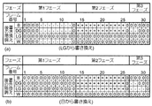
階調制御部502は、画素110の階調を制御するブロックである。階調制御部502は、走査線駆動回路130とデータ線駆動回路140を制御し、電圧Vcom、+15Vの電圧又は−15Vの電圧をフレーム期間において画素電極101dへ印加することにより、画素110の階調を制御する。具体的には、本実施形態においては、階調制御部502は、画像を書き換える書き換え期間において、第1フェーズ、第2フェーズ及び第3フェーズを用いて画像を書き換える。
The
第1フェーズは、書き換え前と書き換え後の階調が異なる画素であって、書き換え前の階調が白以外の画素について、階調を変化させるフェーズである。なお、本実施形態においては、第1フェーズのフレーム数は13フレームとなっている。つまり、画像を書き換えるときの最初のフレームの番号を1とした場合、1〜13番目までのフレームが第1フェーズとなる。 The first phase is a phase in which the gradation is changed for pixels whose gradation before and after rewriting is different and the gradation before rewriting is other than white. In the present embodiment, the number of frames in the first phase is 13 frames. That is, when the number of the first frame when rewriting an image is 1, the first to 13th frames are the first phase.
第2フェーズは、第1フェーズの後、書き換え前の階調より書き換え後の階調が低い画素について、階調を黒へ変化させるフェーズである。なお、本実施形態においては、第2フェーズのフレーム数は13フレームとなっている。画像を書き換えるときの最初のフレームの番号を1とした場合、14〜26番目までのフレームが第2フェーズとなる。 The second phase is a phase in which after the first phase, the gradation is changed to black for pixels whose gradation after rewriting is lower than the gradation before rewriting. In the present embodiment, the number of frames in the second phase is 13 frames. When the number of the first frame when rewriting an image is 1, the 14th to 26th frames are in the second phase.
第3フェーズは、第2フェーズの後、書き換え前の階調より書き換え後の階調が低く、書き換え後にライトグレー又はダークグレーになる画素について、階調を変化させるフェーズである。なお、本実施形態においては、第3フェーズのフレーム数は5フレームとなっている。画像を書き換えるときの最初のフレームの番号を1とした場合、27〜31番目までのフレームが第3フェーズとなる。 The third phase is a phase in which after the second phase, the gradation is changed for a pixel whose gradation after rewriting is lower than the gradation before rewriting and becomes light gray or dark gray after rewriting. In the present embodiment, the number of frames in the third phase is 5 frames. When the number of the first frame when rewriting an image is 1, the 27th to 31st frames are in the third phase.
制御部2は、表示領域100の画像を書き換える場合、画像データをコントローラー5へ出力する。コントローラー5は、制御部2が出力した画像データを取得すると、取得した画像データをRAM501の第1記憶領域に書き込む。なお、第2記憶領域には、画像データを取得する前に表示していた画像の画像データが書き込まれる。階調制御部502は、第1記憶領域に新たな画像データが書き込まれると、画像の書き換え処理を開始する。
The
階調制御部502は、画像の書き換え処理において、複数フレームに渡って画素110の階調を制御するにあたり、何番目のフレームを制御しているかを管理するフレーム番号を初期化して1にする。階調制御部502は、フレーム番号を初期化した後、第1記憶領域と第2記憶領域の画素データを取得する。
In the image rewriting process, the
階調制御部502は、第1記憶領域及び第2記憶領域から取得した画素データと、フレーム番号をLUT503へ出力する。LUT503は、階調制御部502から供給された画素データとフレーム番号に基いて、図6、7のテーブルを参照し、画素電極101dに印加する電圧を示すデータを出力する。階調制御部502は、LUT503から出力されるデータに応じて、画素電極101dへ印加する電圧を指示する信号をデータ線駆動回路140へ出力する。データ線駆動回路140が、走査線112が選択されている期間において、この信号に基いてデータ線114にデータ信号を出力すると、信号に応じた電圧が画素電極101dに印加され、画素の階調が変化する。階調制御部502は、一フレーム期間が終了する毎に、フレーム番号に1を加算し、加算後のフレーム番号のフレームで画素電極101dへ印加する電圧を示すデータをLUT503から取得し、画素110の階調を制御する。階調制御部502は、31フレーム目が終了すると、画像の書き換え処理を終了する。
The
(第1実施形態の動作例)
次に第1実施形態において画素の階調を書き換えるときの動作例について説明する。なお、以下の説明においては、書き換え前の画素の階調が黒の場合、書き換え前の画素の階調がダークグレーの場合、書き換え前の画素の階調がライトグレーの場合、及び書き換え前の画素の階調が白の場合の動作例について説明する。
(Operation example of the first embodiment)
Next, an operation example when rewriting the gradation of a pixel in the first embodiment will be described. In the following description, when the gradation of the pixel before rewriting is black, the gradation of the pixel before rewriting is dark gray, the gradation of the pixel before rewriting is light gray, and the pixel before rewriting An example of the operation when the gradation of white is white will be described.
(書き換え前の画素の階調が黒の場合の動作例)
図8は、画像を書き換えるときに、書き換え前に黒であった画素の階調の遷移を示した図であり、図8(a)は、黒→白の場合、図8(b)は、黒→ライトグレーの場合、図8(c)は、黒→ダークグレーの場合、図8(d)は、黒→黒の場合の遷移を示している。図8及び後述する図9〜11においては、横軸をフレーム番号とし、縦軸を画素の明度(階調)としている。また、図8及び後述する図9〜11においては、図中の「(1)」は、第1フェーズ、「(2)」は、第2フェーズ、「(3)」は、第3フェーズを示している。また、本実施形態においては、図8(a)でフレーム番号が0のときの階調を黒(本実施形態の第1基準階調)、フレーム番号が2のときの階調をダークグレー、フレーム番号が4のときの階調をライトグレー、フレーム番号が12のときの階調を白(本実施形態の第2基準階調)としている。
(Operation example when the gradation of the pixel before rewriting is black)
FIG. 8 is a diagram showing the transition of the gradation of pixels that were black before rewriting when the image was rewritten. FIG. 8A shows the case of black → white, and FIG. In the case of black → light gray, FIG. 8C shows the transition in the case of black → dark gray, and FIG. 8D shows the transition in the case of black → black. In FIG. 8 and FIGS. 9 to 11 described later, the horizontal axis is the frame number, and the vertical axis is the lightness (gradation) of the pixel. In FIG. 8 and FIGS. 9 to 11 to be described later, “(1)” in the figure indicates the first phase, “(2)” indicates the second phase, and “(3)” indicates the third phase. Show. In the present embodiment, in FIG. 8A, the gradation when the frame number is 0 is black (first reference gradation in the present embodiment), the gradation when the frame number is 2 is dark gray, The gradation when the number is 4 is light gray, and the gradation when the frame number is 12 is white (second reference gradation in the present embodiment).
まず、書き換え前の階調が黒であり、書き換え後の階調が白である画素については、LUT503は、図6(a)のテーブルの「W」の行を参照する。この行においては、フレーム番号が1の列から12の列まで「−」が格納されているため、LUT503は、1フレーム目から12フレーム目までは、「−」を出力する。階調制御部502は、当該画素の画素電極101dに印加する電圧を示すデータとして「−」を取得すると、当該画素の画素電極101dへ印加する電圧を−15Vとするよう指示する信号をデータ線駆動回路140へ出力する。データ線駆動回路140が、この信号に基いてデータ線114にデータ信号を出力すると、当該画素に係る走査線112が選択されている期間において、−15Vの電圧が当該画素の画素電極101dに印加され、図8(a)に示したように、1フレーム目から当該画素の階調が白に近づき、12フレーム目で白になる。
また、図6(a)のテーブルの「W」の行でフレーム番号が13以降の列においては、「0」が格納されている。階調制御部502は、当該画素の画素電極101dに印加する電圧を示すデータとして「0」を取得すると、当該画素の画素電極101dへ印加する電圧を電圧Vcomとするよう指示する信号をデータ線駆動回路140へ出力する。データ線駆動回路140が、この信号に基いてデータ線114にデータ信号を出力すると、電圧Vcomが画素電極101dに印加されるため、図8(a)に示したように、13フレーム目以降は、当該画素の階調は、変化しないこととなる。
First, the
Also, “0” is stored in the column “W” in the table of FIG. When the
次に、書き換え前の階調が黒であり、書き換え後の階調がライトグレーである画素については、LUT503は、図6(a)のテーブルの「LG」の行を参照する。この行においては、フレーム番号が1の列から8の列まで「0」が格納されているため、1フレーム目から8フレーム目までは、図8(b)に示したように、当該画素の階調が変化しない。また、図6(a)のテーブルの「LG」の行でフレーム番号が9の列から12の列まで「−」が格納されているため、図8(b)に示したように、9フレーム目から当該画素の階調が白に近づき、12フレーム目でライトグレーになる。また、図6(a)のテーブルの「LG」の行でフレーム番号が13以降の列については、「0」が格納されているため、13フレーム目以降は、当該画素の階調が変化しないこととなる。
Next, the
次に、書き換え前の階調が黒であり、書き換え後の階調がダークグレーである画素については、LUT503は、図6(a)のテーブルの「DG」の行を参照する。この行においては、フレーム番号が1の列から10の列まで「0」が格納されているため、1フレーム目から10フレーム目までは、図8(c)に示したように、当該画素の階調が変化しない。また、図6(a)のテーブルの「DG」の行でフレーム番号が11の列と12の列には「−」が格納されているため、図8(c)に示したように、11フレーム目と12フレーム目で当該画素の階調が白に近づき、12フレーム目でダークグレーになる。また、図6(a)のテーブルの「DG」の行でフレーム番号が13以降の列については、「0」が格納されているため、13フレーム目以降は、当該画素の階調が変化しないこととなる。
Next, the
次に、書き換え前の階調が黒であり、書き換え後の階調も黒である画素については、LUT503は、図6(a)のテーブルの「B」の行を参照する。この行においては、全ての列に「0」が格納されているため、1フレーム目から31フレーム目までは、図8(d)に示したように、当該画素の階調は、書き換え前から変化しないこととなる。
Next, the
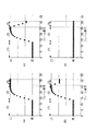
(書き換え前の画素の階調がダークグレーの場合の動作例)
次に、画像の書き換え前の階調がダークグレーの場合の動作例について説明する。書き換え前の階調がダークグレーの場合、LUT503は、図6(b)のテーブルを参照し、画素電極101dに印加する電圧を示すデータを出力する。
(Operation example when the gradation of the pixel before rewriting is dark gray)
Next, an operation example when the gradation before rewriting of the image is dark gray will be described. When the gradation before rewriting is dark gray, the
図9は、画像を書き換えるときに、書き換え前にダークグレーであった画素の階調の遷移を示した図であり、図9(a)は、ダークグレー→白の場合、図9(b)は、ダークグレー→ライトグレーの場合、図9(c)は、ダークグレー→ダークグレーの場合、図9(d)は、ダークグレー→黒の場合の遷移を示している。 FIG. 9 is a diagram showing the transition of the gradation of a pixel that was dark gray before rewriting when the image is rewritten. FIG. 9A shows the case of dark gray → white, and FIG. In the case of dark gray → light gray, FIG. 9C shows the transition in the case of dark gray → dark gray, and FIG. 9D shows the transition in the case of dark gray → black.
まず、書き換え前の階調がダークグレーであり、書き換え後の階調が白である画素については、LUT503は、図6(b)のテーブルの「W」の行を参照する。この行においては、フレーム番号が1の列と2の列には「0」が格納されているため、1フレーム目と2フレーム目では、図9(a)に示したように、当該画素の階調が変化しない。また、図6(b)のテーブルの「W」の行においては、フレーム番号が3の列から12の列まで「−」が格納されているため、図9(a)に示したように、3フレーム目から当該画素の階調が白に近づき、12フレーム目で白になる。また、図6(b)のテーブルの「W」の行でフレーム番号が13以降の列においては、「0」が格納されているため、13フレーム目以降は、当該画素の階調が変化しないこととなる。
First, the
次に、書き換え前の階調がダークグレーであり、書き換え後の階調がライトグレーである画素については、LUT503は、図6(b)のテーブルの「LG」の行を参照する。この行においては、フレーム番号が1の列から10の列までは「0」が格納されているため、1フレーム目から10フレーム目までは、図9(b)に示したように、当該画素の階調が変化しない。また、図6(b)のテーブルの「LG」の行においては、フレーム番号が11の列と12の列で「−」が格納されているため、図9(b)に示したように、11フレーム目から当該画素の階調が白に近づき、12フレーム目でライトグレーになる。また、図6(b)のテーブルの「LG」の行でフレーム番号が13以降の列においては、「0」が格納されているため、図9(b)に示したように、13フレーム目以降は、当該画素の階調は、変化しないこととなる。
Next, the
次に、書き換え前の階調がダークグレーであり、書き換え後の階調もダークグレーである画素については、LUT503は、図6(b)のテーブルの「DG」の行を参照する。
この行においては、全ての列に「0」が格納されているため、1フレーム目から31フレーム目までは、図9(c)に示したように、当該画素の階調が変化しないこととなる。
Next, the
In this row, since “0” is stored in all the columns, the gradation of the pixel does not change from the first frame to the 31st frame as shown in FIG. 9C. Become.
次に、書き換え前の階調がダークグレーであり、書き換え後の階調が黒である画素については、LUT503は、図6(b)のテーブルの「B」の行を参照する。この行においては、フレーム番号が1の列と2の列には「0」が格納されているため、1フレーム目と2フレーム目では、図9(d)に示したように、当該画素の階調が変化しない。また、図6(b)のテーブルの「B」の行においては、フレーム番号が3の列から12の列まで「−」が格納されているため、図9(d)に示したように、3フレーム目から当該画素の階調が白に近づき、12フレーム目で白になる。また、図6(b)のテーブルの「B」の行でフレーム番号が14の列から25の列までは、「+」が格納されている。階調制御部502は、画素電極101dに印加する電圧を示すデータとして「+」を取得すると、当該画素の画素電極101dへ印加する電圧を+15Vとするよう指示する信号をデータ線駆動回路140へ出力する。当該画素に係る走査線112が選択されている期間において、データ線駆動回路140が、この信号に基いてデータ線114にデータ信号を出力すると、+15Vの電圧が当該画素の画素電極101dに印加され、図9(d)に示したように、13フレーム目から当該画素の階調が黒に近づき、25フレーム目で黒となる。なお、図6(b)のテーブルの「B」の行においては、フレーム番号が26の列以降は、「0」が格納されているため、図9(d)に示したように、26フレーム目以降は、当該画素の階調は、変化しないこととなる。
Next, the
(書き換え前の画素の階調がライトグレーの場合の動作例)
次に、画像の書き換え前の階調がライトグレーの場合の動作例について説明する。書き換え前の階調がライトグレーの場合、LUT503は、図7(a)のテーブルを参照し、画素電極101dに印加する電圧を示すデータを出力する。
(Operation example when the gradation of the pixel before rewriting is light gray)
Next, an operation example when the gradation before rewriting of the image is light gray will be described. When the gradation before rewriting is light gray, the
図10は、画像を書き換えるときに、書き換え前にライトグレーであった画素の階調の遷移を示した図であり、図10(a)は、ライトグレー→白の場合、図10(b)は、ライトグレー→ライトグレーの場合、図10(c)は、ライトグレー→ダークグレーの場合、図10(d)は、ライトグレー→黒の場合の遷移を示している。 FIG. 10 is a diagram showing the transition of the gradation of a pixel that was light gray before rewriting when the image is rewritten. FIG. 10A shows the case of light gray → white, and FIG. FIG. 10C shows the transition in the case of light gray → light gray, FIG. 10C shows the transition in the case of light gray → dark gray, and FIG. 10D shows the transition in the case of light gray → black.
まず、書き換え前の階調がライトグレーであり、書き換え後の階調が白である画素については、LUT503は、図7(a)のテーブルの「W」の行を参照する。この行においては、フレーム番号が1の列から4の列までは「0」が格納されているため、1フレーム目から4フレーム目では、図10(a)に示したように、当該画素の階調が変化しない。また、図7(a)のテーブルの「W」の行においては、フレーム番号が5の列から12の列まで「−」が格納されているため、図10(a)に示したように、5フレーム目から当該画素の階調が白に近づき、12フレーム目で白になる。また、図7(a)のテーブルの「W」の行でフレーム番号が13以降の列においては、「0」が格納されているため、図10(a)に示したように、13フレーム目以降は、当該画素の階調は、変化しないこととなる。
First, the
次に、書き換え前の階調がライトグレーであり、書き換え後の階調もライトグレーである画素については、LUT503は、図7(a)のテーブルの「LG」の行を参照する。この行においては、全ての列に「0」が格納されているため、1フレーム目から31フレーム目までは、図10(b)に示したように、当該画素の階調が変化しないこととなる。
Next, the
次に、書き換え前の階調がライトグレーであり、書き換え後の階調がダークグレーである画素については、LUT503は、図7(a)のテーブルの「DG」の行を参照する。この行においては、フレーム番号が1の列から4の列までは「0」が格納されているため、1フレーム目から4フレーム目までは、図10(c)に示したように、当該画素の階調が変化しない。また、図7(a)のテーブルの「DG」の行においては、フレーム番号が5の列から12の列まで「−」が格納されているため、図10(c)に示したように、5フレーム目から当該画素の階調が白に近づき、12フレーム目で白になる。また、図7(a)のテーブルの「DG」の行でフレーム番号が14の列から25の列までは、「+」が格納されているため、図10(c)に示したように、14フレーム目から当該画素の階調が黒に近づき、25フレーム目で黒となる。また、図7(a)のテーブルの「DG」の行でフレーム番号が27の列と28の列においては、「−」が格納されているため、図10(c)に示したように、27フレーム目から当該画素の階調が白に近づき、28フレーム目でダークグレーになる。なお、図7(a)のテーブルの「DG」の行でフレーム番号が29以降の列においては、「0」が格納されているため、図10(c)に示したように、29フレーム目以降は、当該画素の階調は、変化しないこととなる。
Next, the
次に、書き換え前の階調がライトグレーであり、書き換え後の階調が黒である画素については、LUT503は、図7(a)のテーブルの「B」の行を参照する。この行においては、フレーム番号が1の列から4の列までは「0」が格納されているため、1フレーム目から4フレーム目までは、図10(d)に示したように、当該画素の階調が変化しない。また、図7(a)のテーブルの「B」の行においては、フレーム番号が5の列から12の列まで「−」が格納されているため、図10(d)に示したように、5フレーム目から当該画素の階調が白に近づき、12フレーム目で白になる。また、図7(a)のテーブルの「B」の行でフレーム番号が14の列から25の列までは、「+」が格納されているため、14フレーム目から当該画素の階調が黒に近づき、25フレーム目で黒となる。なお、図7(a)のテーブルの「B」の行においては、フレーム番号が26の列以降は、「0」が格納されているため、図10(d)に示したように、26フレーム目以降は、当該画素の階調は、変化しないこととなる。
Next, the
(書き換え前の画素の階調が白の場合の動作例)
次に、画像の書き換え前の階調が白の場合の動作例について説明する。書き換え前の階調が白の場合、LUT503は、図7(b)のテーブルを参照し、画素電極101dに印加する電圧を示すデータを出力する。
(Operation example when the gradation of the pixel before rewriting is white)
Next, an operation example when the gradation before rewriting of the image is white will be described. When the gradation before rewriting is white, the
図11は、画像を書き換えるときに、書き換え前に白であった画素の階調の遷移を示した図であり、図11(a)は、白→白の場合、図11(b)は、白→ライトグレーの場合、図11(c)は、白→ダークグレーの場合、図11(d)は、白→黒の場合の遷移を示している。 FIG. 11 is a diagram showing the transition of the gradation of pixels that were white before rewriting when the image was rewritten. FIG. 11A shows the case of white → white, and FIG. In the case of white → light gray, FIG. 11C shows a transition in the case of white → dark gray, and FIG. 11D shows the transition in the case of white → black.
まず、書き換え前の階調が白であり、書き換え後の階調も白である画素については、LUT503は、図7(b)のテーブルの「W」の行を参照する。この行においては、全ての列に「0」が格納されているため、1フレーム目から31フレーム目までは、図11(a)に示したように、当該画素の階調が変化しないこととなる。
First, the
次に、書き換え前の階調が白であり、書き換え後の階調がライトグレーである画素については、LUT503は、図7(b)のテーブルの「LG」の行を参照する。この行においては、フレーム番号が1の列から13の列までは「0」が格納されているため、1フレーム目から13フレーム目までは、図11(b)に示したように、当該画素の階調が変化しない。また、図7(b)のテーブルの「LG」の行においては、フレーム番号が14の列から25の列まで「+」が格納されているため、図11(b)に示したように、14フレーム目から当該画素の階調が黒に近づき、25フレーム目で黒となる。また、図7(b)のテーブルの「LG」の行でフレーム番号が27の列から30の列までは、「−」が格納されているため、図11(b)に示したように、27フレーム目から当該画素の階調が白に近づき、30フレーム目でライトグレーになる。なお、図7(b)のテーブルの「LG」の行でフレーム番号が31の列においては、「0」が格納されているため、図11(b)に示したように、31フレーム目では、当該画素の階調は、変化しないこととなる。
Next, the
次に、書き換え前の階調が白であり、書き換え後の階調がダークグレーである画素については、LUT503は、図7(b)のテーブルの「DG」の行を参照する。この行においては、フレーム番号が1の列から13の列までは「0」が格納されているため、1フレーム目から13フレーム目までは、図11(c)に示したように、当該画素の階調が変化しない。また、図7(b)のテーブルの「DG」の行でフレーム番号が14の列から25の列までは、「+」が格納されているため、図11(c)に示したように、14フレーム目から当該画素の階調が黒に近づき、25フレーム目で黒となる。また、図7(b)のテーブルの「DG」の行でフレーム番号が27の列と28の列においては、「−」が格納されているため、図11(c)に示したように、27フレーム目から画素の階調が白に近づき、28フレーム目でダークグレーになる。なお、図7(b)のテーブルの「DG」の行でフレーム番号が28の列以降においては、「0」が格納されているため、図11(c)に示したように、28フレーム目以降では、当該画素の階調は、変化しないこととなる。
Next, the
次に、書き換え前の階調が白であり、書き換え後の階調が黒である画素については、LUT503は、図7(b)のテーブルの「B」の行を参照する。の行においては、フレーム番号が1の列から13の列までは「0」が格納されているため、1フレーム目から13フレーム目までは、図11(d)に示したように、当該画素の階調が変化しない。また、図7(b)のテーブルの「B」の行でフレーム番号が14の列から25の列までは、「+」が格納されているため、図11(d)に示したように、14フレーム目から当該画素の階調が黒に近づき、25フレーム目で黒となる。また、図7(b)のテーブルの「B」の行でフレーム番号が26の列以降においては、「0」が格納されているため、図11(d)に示したように、26フレーム目以降では、当該画素の階調は、変化しないこととなる。
Next, the
以上説明したように、本実施形態においては、低階調側(黒側:第1基準階調側)から高階調側(白側:第2基準階調側)へ階調を変化させる画素については、白を経由せずに階調が変化するため、白を経由する構成と比較すると、画像の書き換え中において、画素の階調の変化が目立たなくなる。
また、本実施形態においては、画像を書き換える際には、全画素に対し、各フェーズの最後のフレーム、即ち、13フレーム目、26フレーム目、31フレーム目で電圧Vcomが画素電極101dへ印加される。これにより、各フェーズを開始するときには、電気泳動粒子が止まっているため、全ての画素110で電気泳動粒子の動きやすさが同じ状態から階調の制御を行うこととなり、同じ階調を表示する画素110同士においては階調に差が生じにくくなる。
また、本実施形態においては、ライトグレーとダークグレーを表示する際には、高階調側からはライトグレーやダークグレーにはせず、いずれも低階調側から−15Vの電圧を画素電極101dに印加し、電圧の印加回数を異ならせることにより階調を制御するため、ライトグレーとダークグレーの階調差にバラつきが生じにくくなる。
As described above, in the present embodiment, the pixel that changes the gradation from the low gradation side (black side: first reference gradation side) to the high gradation side (white side: second reference gradation side). Since the gradation changes without going through white, the change in the gradation of the pixel becomes inconspicuous during the rewriting of the image as compared with the configuration through white.
Further, in this embodiment, when rewriting an image, the voltage Vcom is applied to the
In this embodiment, when light gray and dark gray are displayed, neither light gray nor dark gray is applied from the high gradation side, and a voltage of −15 V is applied to the
[第2実施形態]
次に、本発明の第2実施形態について説明する。本発明の第2実施形態は、第1実施形態と比較すると、LUT503の構成が第1実施形態と異なる。以下、第1実施形態と同じ構成については説明を省略し、相違点について説明する。
[Second Embodiment]
Next, a second embodiment of the present invention will be described. The second embodiment of the present invention differs from the first embodiment in the configuration of the
本実施形態の第1フェーズは、書き換え前と書き換え後の階調が異なる画素であって、書き換え前の階調が黒以外の画素について、階調を変化させるフェーズである。本実施形態においても、画像を書き換えるときの最初のフレームの番号を1とした場合、1〜13番目までのフレームが第1フェーズとなる。 The first phase of the present embodiment is a phase in which the gradation is changed for a pixel whose gradation before and after rewriting is different and whose gradation before rewriting is other than black. Also in this embodiment, when the number of the first frame when rewriting an image is 1, the first to 13th frames are in the first phase.
本実施形態の第2フェーズは、第1フェーズの後、書き換え前の階調より書き換え後の階調が高い画素について、階調を白へ変化させるフェーズである。本実施形態においても、画像を書き換えるときの最初のフレームの番号を1とした場合、14〜26番目までのフレームが第2フェーズとなる。 The second phase of the present embodiment is a phase in which after the first phase, the gradation is changed to white for pixels whose gradation after rewriting is higher than the gradation before rewriting. Also in the present embodiment, when the number of the first frame when rewriting an image is 1, the 14th to 26th frames are in the second phase.
本実施形態の第3フェーズは、第2フェーズの後、書き換え前の階調より書き換え後の階調が高く、書き換え後にライトグレー又はダークグレーとなる画素について、階調を変化させるフェーズである。本実施形態においても、第3フェーズのフレーム数は5フレームとなっている。画像を書き換えるときの最初のフレームの番号を1とした場合、27〜31番目までのフレームが第3フェーズとなる。 The third phase of the present embodiment is a phase in which after the second phase, the gradation after the rewriting is higher than the gradation before the rewriting, and the gradation is changed for pixels that become light gray or dark gray after the rewriting. Also in this embodiment, the number of frames in the third phase is 5 frames. When the number of the first frame when rewriting an image is 1, the 27th to 31st frames are in the third phase.
図12、13は、本実施形態に係るLUT503が記憶しているテーブルを示した図である。図12、13に示したように、本実施形態においては、各フェーズにおいて画素の階調を変化させるときに画素電極101dへ印加する電圧の極性が第1実施形態と異なる。具体的には、第1フェーズで画素の階調を変化させる場合、正極性の電圧を画素電極101dへ印加し、第2フェーズで画素の階調を変化させる場合、負極性の電圧を画素電極101dへ印加する。また、第3フェーズで画素の階調を変化させる場合、正極性の電圧を画素電極101dへ印加する。
12 and 13 are diagrams showing tables stored in the
(第2実施形態の動作例)
次に第1実施形態において画素の階調を書き換えるときの動作例について説明する。なお、以下の説明においては、書き換え前の画素の階調が黒の場合、書き換え前の画素の階調がダークグレーの場合、書き換え前の画素の階調がライトグレーの場合、及び書き換え前の画素の階調が白の場合の動作例について説明する。
(Operation example of the second embodiment)
Next, an operation example when rewriting the gradation of a pixel in the first embodiment will be described. In the following description, when the gradation of the pixel before rewriting is black, the gradation of the pixel before rewriting is dark gray, the gradation of the pixel before rewriting is light gray, and the pixel before rewriting An example of the operation when the gradation of white is white will be described.
図14は、画像を書き換えるときに、書き換え前に白であった画素の階調の遷移を示した図であり、図14(a)は、白→白の場合、図14(b)は、白→ライトグレーの場合、図14(c)は、白→ダークグレーの場合、図14(d)は、白→黒の場合の遷移を示している。図14及び後述する図15〜17においては、横軸をフレーム番号とし、縦軸を画素の明度(階調)としている。また、図14及び後述する図15〜17においては、図中の「(1)」は、第1フェーズ、「(2)」は、第2フェーズ、「(3)」は、第3フェーズを示している。また、本実施形態においては、図14(d)でフレーム番号が0のときの階調を白(本実施形態の第1基準階調)、フレーム番号が2のときの階調をライトグレー、フレーム番号が4のときの階調をダークグレー、フレーム番号が12のときの階調を黒(本実施形態の第2基準階調)としている。 FIG. 14 is a diagram showing the transition of the gradation of pixels that were white before rewriting when the image was rewritten. FIG. 14A shows the case of white → white, and FIG. In the case of white → light gray, FIG. 14C shows the transition in the case of white → dark gray, and FIG. 14D shows the transition in the case of white → black. In FIG. 14 and FIGS. 15 to 17 described later, the horizontal axis is the frame number, and the vertical axis is the lightness (gradation) of the pixel. In FIG. 14 and FIGS. 15 to 17 to be described later, “(1)” in the figure indicates the first phase, “(2)” indicates the second phase, and “(3)” indicates the third phase. Show. In the present embodiment, the gray level when the frame number is 0 in FIG. 14D is white (first reference gray level in the present embodiment), and the gray level when the frame number is 2 is light gray. The gradation when the frame number is 4 is dark gray, and the gradation when the frame number is 12 is black (second reference gradation in the present embodiment).
まず、書き換え前の階調が白であり、書き換え後の階調が白である画素については、LUT503は、図13(b)のテーブルの「W」の行を参照する。この行においては、全ての列に「0」が格納されているため、1フレーム目から31フレーム目までは、図14(a)に示したように、当該画素の階調が変化しないこととなる。
First, the
次に、書き換え前の階調が白であり、書き換え後の階調がライトグレーである画素については、LUT503は、図13(b)のテーブルの「LG」の行を参照する。この行においては、フレーム番号が1の列から10列までは「0」が格納されているため、1フレーム目から10フレーム目までは、図14(b)に示したように、当該画素の階調が変化しない。また、図13(b)のテーブルの「LG」の行においては、フレーム番号が11の列と12の列で「+」が格納されているため、11フレーム目から当該画素の階調が黒に近づき、12フレーム目でライトグレーになる。また、図13(b)のテーブルの「LG」の行でフレーム番号が13以降の列においては、「0」が格納されているため、図14(b)に示したように、13フレーム目以降は、当該画素の階調は、変化しないこととなる。
Next, the
次に、書き換え前の階調が白であり、書き換え後の階調がダークグレーである画素については、LUT503は、図13(b)のテーブルの「DG」の行を参照する。この行においては、フレーム番号が1の列から8の列までは「0」が格納されているため、1フレーム目から8フレーム目までは、図14(c)に示したように、当該画素の階調が変化しない。また、図13(b)のテーブルの「DG」の行においては、フレーム番号が9の列から12の列まで「+」が格納されているため、図14(c)に示したように、9フレーム目から当該画素の階調が黒に近づき、12フレーム目でダークグレーになる。また、図13(b)のテーブルの「DG」の行でフレーム番号が13以降の列においては、「0」が格納されているため、図14(c)に示したように、13フレーム目以降は、当該画素の階調は、変化しないこととなる。
Next, the
次に、書き換え前の階調が白であり、書き換え後の階調が黒である画素については、LUT503は、図13(b)のテーブルの「B」の行を参照する。この行においては、フレーム番号が1の列から12の列まで「+」が格納されているため、図14(d)に示したように、1フレーム目から当該画素の階調が黒に近づき、12フレーム目で黒になる。また、図13(b)のテーブルの「B」の行でフレーム番号が13以降の列においては「0」が格納されているため、図14(d)に示したように、13フレーム目以降は、当該画素の階調は、変化しないこととなる。
Next, the
(書き換え前の画素の階調がライトグレーの場合の動作例)
次に、画像の書き換え前の階調がライトグレーの場合の動作例について説明する。書き換え前の階調がライトグレーの場合、LUT503は、図13(a)のテーブルを参照し、画素電極101dに印加する電圧を示すデータを出力する。
(Operation example when the gradation of the pixel before rewriting is light gray)
Next, an operation example when the gradation before rewriting of the image is light gray will be described. When the gradation before rewriting is light gray, the
図15は、画像を書き換えるときに、書き換え前にライトグレーであった画素の階調の遷移を示した図であり、図15(a)は、ライトグレー→白の場合、図15(b)は、ライトグレー→ライトグレーの場合、図15(c)は、ライトグレー→ダークグレーの場合、図15(d)は、ライトグレー→黒の場合の遷移を示している。 FIG. 15 is a diagram showing the transition of the gradation of a pixel that was light gray before rewriting when the image is rewritten. FIG. 15A shows the case of light gray → white, FIG. FIG. 15C shows the transition in the case of light gray → light gray, FIG. 15C shows the transition in the case of light gray → dark gray, and FIG. 15D shows the transition in the case of light gray → black.
まず、書き換え前の階調がライトグレーであり、書き換え後の階調が白である画素については、LUT503は、図13(a)のテーブルの「W」の行を参照する。この行においては、フレーム番号が1の列と2の列では「0」が格納されているため、1フレーム目と2フレーム目では、図15(a)に示したように、当該画素の階調が変化しない。また、図13(a)のテーブルの「W」の行においては、フレーム番号が3の列から12の列まで「+」が格納されているため、図15(a)に示したように、3フレーム目から当該画素の階調が黒に近づき、12フレーム目で黒になる。また、図13(a)のテーブルの「W」の行でフレーム番号が14の列から25の列までは、「−」が格納されているため、図15(a)に示したように、14フレーム目から当該画素の階調が白に近づき、25フレーム目で白となる。また、図13(a)のテーブルの「W」の行でフレーム番号が26以降の列においては、「0」が格納されているため、図15(a)に示したように、26フレーム目以降は、当該画素の階調は、変化しないこととなる。
First, the
次に、書き換え前の階調がライトグレーであり、書き換え後の階調もライトグレーである画素については、LUT503は、図13(a)のテーブルの「LG」の行を参照する。この行においては、全て「0」が格納されている。このため、1フレーム目から31フレーム目までは、図15(b)に示したように、当該画素の階調が変化しないこととなる。
Next, the
次に、書き換え前の階調がライトグレーであり、書き換え後の階調がダークグレーである画素については、LUT503は、図13(a)のテーブルの「DG」の行を参照する。この行においては、フレーム番号が1の列から10列までは「0」が格納されているため、1フレーム目から10フレーム目までは、図15(c)に示したように、当該画素の階調が変化しない。また、図13(a)のテーブルの「DG」の行においては、フレーム番号が11の列と12の列で「+」が格納されているため、図15(c)に示したように、11フレーム目から当該画素の階調が黒に近づき、12フレーム目でダークグレーになる。また、図13(a)のテーブルの「DG」の行でフレーム番号が13以降の列においては、「0」が格納されているため、図15(c)に示したように、13フレーム目以降は、当該画素の階調は、変化しないこととなる。
Next, the
次に、書き換え前の階調がライトグレーであり、書き換え後の階調が黒である画素については、LUT503は、図13(a)のテーブルの「B」の行を参照する。この行においては、フレーム番号が1の列と2の列では「0」が格納されているため、1フレーム目と2フレーム目では、図15(d)に示したように、当該画素の階調が変化しない。
また、図13(a)のテーブルの「B」の行においては、フレーム番号が3の列から12の列まで「+」が格納されているため、図15(d)に示したように、3フレーム目から当該画素の階調が黒に近づき、12フレーム目で黒になる。また、図13(a)のテーブルの「B」の行でフレーム番号が13以降の列においては、「0」が格納されている。このため、図15(d)に示したように、13フレーム目以降は、当該画素の階調は、変化しないこととなる。
Next, the
Further, in the row “B” in the table of FIG. 13A, “+” is stored from the column of the
(書き換え前の画素の階調がダークグレーの場合の動作例)
次に、画像の書き換え前の階調がダークグレーの場合の動作例について説明する。書き換え前の階調がダークグレーの場合、LUT503は、図12(b)のテーブルを参照し、画素電極101dに印加する電圧を示すデータを出力する。
(Operation example when the gradation of the pixel before rewriting is dark gray)
Next, an operation example when the gradation before rewriting of the image is dark gray will be described. When the gradation before rewriting is dark gray, the
図16は、画像を書き換えるときに、書き換え前にダークグレーであった画素の階調の遷移を示した図であり、図16(a)は、ダークグレー→白の場合、図16(b)は、ダークグレー→ライトグレーの場合、図16(c)は、ダークグレー→ダークグレーの場合、図16(d)は、ダークグレー→黒の場合の遷移を示している。 FIG. 16 is a diagram showing the transition of the gradation of pixels that were dark gray before rewriting when the image is rewritten. FIG. 16A shows the case of dark gray → white, and FIG. In the case of dark gray → light gray, FIG. 16C shows the transition in the case of dark gray → dark gray, and FIG. 16D shows the transition in the case of dark gray → black.
まず、書き換え前の階調がダークグレーであり、書き換え後の階調が白である画素については、LUT503は、図12(b)のテーブルの「W」の行を参照する。この行においては、フレーム番号が1の列から4の列までは「0」が格納されているため、1フレーム目から4フレーム目までは、図16(a)に示したように、当該画素の階調が変化しない。また、図12(b)のテーブルの「W」の行においては、フレーム番号が5の列から12の列まで「+」が格納されているため、図16(a)に示したように、5フレーム目から当該画素の階調が黒に近づき、12フレーム目で黒になる。また、図12(b)のテーブルの「W」の行でフレーム番号が14の列から25の列までは、「−」が格納されているため、図16(a)に示したように、14フレーム目から当該画素の階調が白に近づき、25フレーム目で白となる。また、図12(b)のテーブルの「W」の行でフレーム番号が26以降の列においては、「0」が格納されているため、図16(a)に示したように、26フレーム目以降は、当該画素の階調は、変化しないこととなる。
First, the
次に、書き換え前の階調がダークグレーであり、書き換え後の階調がライトグレーである画素については、LUT503は、図12(b)のテーブルの「LG」の行を参照する。この行においては、フレーム番号が1の列から4の列までは「0」が格納されているため、1フレーム目から4フレーム目までは、図16(b)に示したように、当該画素の階調が変化しない。また、図12(b)のテーブルの「LG」の行においては、フレーム番号が5の列から12の列まで「+」が格納されているため、図16(b)に示したように、5フレーム目から当該画素の階調が黒に近づき、12フレーム目で黒になる。また、図12(b)のテーブルの「LG」の行でフレーム番号が14の列から25の列までは、「−」が格納されているため、図16(b)に示したように、14フレーム目から当該画素の階調が白に近づき、25フレーム目で白となる。また、図12(b)のテーブルの「LG」の行でフレーム番号が27の列と28の列においては、「+」が格納されているため、図16(b)に示したように、27フレーム目から当該画素の階調が黒に近づき、28フレーム目でライトグレーになる。また、図12(b)のテーブルの「W」の行でフレーム番号が29以降の列においては、「0」が格納されているため、図16(b)に示したように、29フレーム目以降は、当該画素の階調は、変化しないこととなる。
Next, the
次に、書き換え前の階調がダークグレーであり、書き換え後の階調もダークグレーである画素については、LUT503は、図12(b)のテーブルの「DG」の行を参照する。この行においては、全て「0」が格納されているため、1フレーム目から31フレーム目までは、図16(c)に示したように、当該画素の階調が変化しないこととなる。
Next, the
次に、書き換え前の階調がダークグレーであり、書き換え後の階調が黒である画素については、LUT503は、図12(b)のテーブルの「B」の行を参照する。この行においては、フレーム番号が1の列から4の列までは「0」が格納されているため、1フレーム目から4フレーム目までは、図16(d)に示したように、当該画素の階調が変化しない。また、図12(b)のテーブルの「B」の行においては、フレーム番号が5の列から12の列まで「+」が格納されているため、図16(d)に示したように、5フレーム目から当該画素の階調が黒に近づき、12フレーム目で黒になる。また、図12(b)のテーブルの「B」の行でフレーム番号が13以降の列においては、「0」が格納されているため、図16(d)に示したように、13フレーム目以降は、当該画素の階調は、変化しないこととなる。
Next, the
(書き換え前の画素の階調が黒の場合の動作例)
次に、画像の書き換え前の階調が黒の場合の動作例について説明する。書き換え前の階調が白の場合、LUT503は、図12(a)のテーブルを参照する。
(Operation example when the gradation of the pixel before rewriting is black)
Next, an operation example when the gradation before rewriting of the image is black will be described. When the gradation before rewriting is white, the
図17は、画像を書き換えるときに、書き換え前に黒であった画素の階調の遷移を示した図であり、図17(a)は、黒→白の場合、図17(b)は、黒→ライトグレーの場合、図17(c)は、黒→ダークグレーの場合、図17(d)は、黒→黒の場合の遷移を示している。 FIG. 17 is a diagram showing the transition of the gradation of pixels that were black before rewriting when the image was rewritten. FIG. 17A shows the case of black → white, and FIG. In the case of black → light gray, FIG. 17C shows a transition in the case of black → dark gray, and FIG. 17D shows the transition in the case of black → black.
まず、書き換え前の階調が黒であり、書き換え後の階調が白である画素については、LUT503は、図12(a)のテーブルの「W」の行を参照する。この行においては、フレーム番号が1の列から13の列までは「0」が格納されているため、1フレーム目から13フレーム目までは、図17(a)に示したように、当該画素の階調が変化しない。また、図12(a)のテーブルの「B」の行でフレーム番号が14の列から25の列までは、「−」が格納されているため、図17(a)に示したように、14フレーム目から当該画素の階調が白に近づき、25フレーム目で白となる。また、図12(a)のテーブルの「B」の行でフレーム番号が26の列以降においては、「0」が格納されているため、図17(a)に示したように、26フレーム目以降では、当該画素の階調は、変化しないこととなる。
First, the
次に、書き換え前の階調が白であり、書き換え後の階調がライトグレーである画素については、LUT503は、図12(a)のテーブルの「LG」の行を参照する。この行においては、フレーム番号が1の列から13の列までは「0」が格納されているため、1フレーム目から13フレーム目までは、図17(b)に示したように、当該画素の階調が変化しない。また、図12(a)のテーブルの「LG」の行でフレーム番号が14の列から25の列までは、「−」が格納されているため、、図17(b)に示したように、14フレーム目から当該画素の階調が白に近づき、25フレーム目で白となる。また、図12(a)のテーブルの「LG」の行でフレーム番号が27の列と28の列においては、「+」が格納されているため、図17(b)に示したように、27フレーム目から当該画素の階調が黒に近づき、28フレーム目でライトグレーになる。なお、図12(a)のテーブルの「LG」の行でフレーム番号が28の列以降においては、「0」が格納されているため、図17(b)に示したように、28フレーム目以降では、当該画素の階調は、変化しないこととなる。
Next, the
次に、書き換え前の階調が黒であり、書き換え後の階調がダークグレーである画素については、LUT503は、図12(a)のテーブルの「DG」の行を参照する。この行においては、フレーム番号が1の列から13の列までは「0」が格納されているため、1フレーム目から13フレーム目までは、図17(c)に示したように、当該画素の階調が変化しない。また、図12(a)のテーブルの「DG」の行でフレーム番号が14の列から25の列までは、「−」が格納されているため、図17(c)に示したように、14フレーム目から当該画素の階調が白に近づき、25フレーム目で白となる。また、図12(a)のテーブルの「DG」の行でフレーム番号が27の列から30の列においては、「+」が格納されているため、図17(c)に示したように、27フレーム目から当該画素の階調が黒に近づき、30フレーム目でダークグレーになる。なお、図12(a)のテーブルの「DG」の行でフレーム番号が31の列においては、「0」が格納されているため、図17(c)に示したように、31フレーム目では、当該画素の階調は、変化しないこととなる。
Next, the
次に、書き換え前の階調が黒であり、書き換え後の階調も黒である画素については、LUT503は、図12(a)のテーブルの「B」の行を参照する。この行においては、全て「0」が格納されているため、1フレーム目から31フレーム目までは、図17(d)に示したように、当該画素の階調が変化しないこととなる。
Next, the
以上説明したように、本実施形態においては、高階調側(白側:第1基準階調側)から低階調側(黒側:第2基準階調側)へ階調を変化させる画素については、黒を経由せずに階調が変化するため、黒を経由する構成と比較すると、画像の書き換え中において、画素の階調の変化が目立たなくなる。
また、本実施形態においても、画像を書き換える際には、全画素に対し、各フェーズの最後のフレーム、即ち、13フレーム目、26フレーム目、31フレーム目で電圧Vcomが画素電極101dへ印加される。これにより、各フェーズを開始するときには、電気泳動粒子が止まっているため、全ての画素110で電気泳動粒子の動きやすさが同じ状態から階調の制御を行うこととなり、同じ階調を表示する画素110同士においては階調に差が生じにくくなる。
また、本実施形態においては、ライトグレーとダークグレーを表示する際には、低階調側からはライトグレーやダークグレーにはせず、いずれも高階調側から+15Vの電圧を画素電極101dに印加し、電圧の印加回数を異ならせることにより階調を制御するため、ライトグレーとダークグレーの階調差にバラつきが生じにくくなる。
As described above, in the present embodiment, the pixel that changes the gradation from the high gradation side (white side: first reference gradation side) to the low gradation side (black side: second reference gradation side). Since the gradation changes without going through black, the change in the gradation of the pixel becomes inconspicuous during the rewriting of the image as compared with the configuration through black.
Also in this embodiment, when rewriting an image, the voltage Vcom is applied to the
In this embodiment, when displaying light gray and dark gray, light gray or dark gray is not applied from the low gradation side, and a voltage of +15 V is applied to the
[電子機器]
次に、上述した実施形態に係る表示装置1000を適用した電子機器の例について説明する。図18は、上述した実施形態に係る表示装置1000を用いた電子ブックリーダーの外観を示した図である。電子ブックリーダー2000は、板状のフレーム2001と、ボタン9A〜9Fと、上述した実施形態に係る電気光学装置1と制御部2を備えている。電子ブックリーダー2000においては表示領域100が露出している。電子ブックリーダー2000においては、電子書籍の内容が表示領域100に表示され、ボタン9A〜9Fを操作することにより電子書籍のページがめくられる。なお、このほかにも、上述した実施形態に係る電気光学装置1が適用可能な電子機器としては、時計や、電子ペーパー、電子手帳、電卓、携帯電話機等などが挙げられる。
[Electronics]
Next, an example of an electronic apparatus to which the
[変形例]
以上、本発明の実施形態について説明したが、本発明は上述した実施形態に限定されることなく、他の様々な形態で実施可能である。例えば、上述の実施形態を以下のように変形して本発明を実施してもよい。なお、上述した実施形態及び以下の変形例は、各々を組み合わせてもよい。
[Modification]
As mentioned above, although embodiment of this invention was described, this invention is not limited to embodiment mentioned above, It can implement with another various form. For example, the present invention may be implemented by modifying the above-described embodiment as follows. In addition, you may combine each of embodiment mentioned above and the following modifications.
上述した実施形態においては、表示領域100の全ての画素110に対して第1フェーズ〜第3フェーズを実行し、表示する画像を書き換えているが、この構成に限定されるものではない。例えば、画像を書き換える際に書き換え前と書き換え後とで階調の変化が生じる領域を特定し、特定した領域については、上記の三つのフェーズを実行し、他の領域にある画素110については、画素電極101dに電圧Vcomを印加するようにしてもよい。
In the above-described embodiment, the first phase to the third phase are executed on all the
本発明においては、各フェーズにおけるフレーム数は、上述した数に限定されるものはなく、他の数であってもよい。また、上述した実施形態においては、階調を白から黒にするときに画素電極101dに+15Vの電圧を12回印加しているが、11回以下又は13回以上であってもよい。また、上述した実施形態においては、階調を黒から白にするときに画素電極101dに−15Vの電圧を12回印加しているが、11回以下又は13回以上であってもよい。また、中間調を表示する際に印加する−15V又は+15Vの電圧の印加回数についても、上述した実施形態の数に限定されるものではなく、他の印加回数であってもよい。
また、上述した実施形態においては、温度センサーで表示領域100の温度を測定し、測定した温度に応じて、各フェーズにおけるフレーム数、+15Vや−15Vの電圧の印加回数を変更するようにしてもよい。
In the present invention, the number of frames in each phase is not limited to the number described above, and may be other numbers. In the embodiment described above, when the gradation is changed from white to black, the voltage of +15 V is applied 12 times to the
In the above-described embodiment, the temperature of the
上述した実施形態においては、アクティブマトリックス型の電気光学装置を例に説明したが、これに限定する趣旨ではない。電気光学装置は、第1電極としてセグメント電極を有するセグメント型の構成であってもよい。この場合、セグメント電極に電圧を印加する時間に応じて電気泳動粒子の移動距離、すなわち階調変化の大きさが決まる。このため、上記実施形態の説明において、画素電極101dに電圧を印加するフレーム数を、セグメント電極へ電圧を印加する時間と読み替えればセグメント型の電気光学装置の実施形態とすることができる。セグメント型の電気光学装置では、階調制御部は、画素の階調を変化させる電圧を、変化させる階調差に応じた印加時間だけセグメント電極へ印加し、当該階調差が大きい画素ほど、電圧の印加時間を長くする。
In the above-described embodiments, the active matrix type electro-optical device has been described as an example, but the present invention is not limited to this. The electro-optical device may have a segment type configuration having a segment electrode as the first electrode. In this case, the moving distance of the electrophoretic particles, that is, the magnitude of the gradation change is determined according to the time during which the voltage is applied to the segment electrode. For this reason, in the description of the above-described embodiment, if the number of frames in which the voltage is applied to the
上述した実施形態においては、電気光学装置として電気泳動層102を有するものを例に説明したが、これに限定する趣旨ではない。電気光学装置は、画素の表示状態を変化させるための書き込みが、電圧を複数回印加する書き込み動作によって行われるものであればどのようなものであってもよく、例えば電気光学材料として電子粉流体を用いた電気光学装置であってもよい。
In the above-described embodiment, the electro-optical device having the
上述した実施形態においては、電気光学装置1は、黒、ダークグレー、ライトグレー、白の4階調を表示する構成となっているが、表示する階調は4階調に限定されるものではない。例えば、ダークグレー又はライトグレーのいずれか一方を表示しない構成、即ち、3階調を表示する構成としてもよい。また、中間調としてダークグレーやライトグレー以外の階調も表示し、5階調以上の階調を表示するようにしてもよい。
In the embodiment described above, the electro-
上述した実施形態においては、各フェーズの最後のフレームで画素電極101dに電圧Vcomを印加する構成となっているが、この構成に限定されるものではない。例えば、3つのフェーズの少なくとも1つのフェーズの最後のフレームで画素電極101dに電圧Vcomを印加する構成であってもよい。
In the embodiment described above, the voltage Vcom is applied to the
上述した電子ブックリーダー2000においては、第1実施形態の動作と第2実施形態の動作のいずれの動作を行うか、ボタン操作して設定するようにしてもよい。
例えば、文書を表示する場合、背景色を白とし、文字を黒又は中間調とする場合には、第1実施形態の動作を行うように設定し、背景色を黒とし、文字を白又は中間調とする場合には、第2実施形態の動作を行うように設定してもよい。
In the
For example, when displaying a document, when the background color is white and the character is black or halftone, the operation of the first embodiment is set so that the background color is black and the character is white or intermediate. In the case of a key, it may be set to perform the operation of the second embodiment.
上述した実施形態においては、黒の画素の画素電極101dへ−15Vの電圧を印加した場合と、白の画素の画素電極101dへ−15Vの電圧を印加した場合とで、階調の変化量が異なる場合がある。例えば、黒の画素の画素電極101dへ−15Vの電圧を一回印加したときの黒からの階調の変化量が、白の画素の画素電極101dへ+15Vの電圧を一回印加したときの白からの階調の変化量より小さい場合、第1実施形態の動作を行うようにしてもよい。また、例えば、白の画素の画素電極101dへ+15Vの電圧を一回印加したときの白からの階調の変化量が、黒の画素の画素電極101dへ−15Vの電圧を一回印加したときの黒からの階調の変化量より小さい場合、第2実施形態の動作を行うようにしてもよい。
In the embodiment described above, the amount of change in gradation is different between a case where a voltage of −15 V is applied to the
1…電気光学装置、2…制御部、5…コントローラー、10…表示部、100…表示領域、101…第1基板、101a…基板、101b…接着層、101c…回路層、101d…画素電極、102…電気泳動層、102a…マイクロカプセル、102b…バインダー、103…第2基板、103a…フィルム、103b…共通電極層、110…画素、110a…TFT、110b…表示素子、110c…補助容量、112…走査線、114…データ線、130…走査線駆動回路、140…データ線駆動回路、501…RAM、502…階調制御部、503…LUT、1000…表示装置、2000…電子ブックリーダー、2001…フレーム
DESCRIPTION OF
Claims (10)
前記画素により表示される画像を書き換える階調制御部を有し、
前記階調制御部は、前記画像を書き換える場合、
書き換え後の階調が書き換え前の階調より第2基準階調側の画素については、前記画素の階調を前記第2基準階調側へ変化させる電圧を、書き換え前の階調と書き換え後の階調との階調差に応じた印加回数で、前記第1電極へ印加し、
書き換え後の階調が書き換え前の階調より第1基準階調側の画素については、前記画素の階調を前記第2基準階調へ変化させてから前記第1基準階調へ変化させた後、前記画素の階調を前記第2基準階調側へ変化させる電圧を、書き換え後の階調に応じた印加回数で、前記第1電極へ印加する
電気光学装置。 A first electrode provided in a plurality of pixels, a second electrode disposed opposite to the first electrode, and an electro-optic having memory property disposed between the first electrode and the second electrode An electro-optical device comprising a material,
A gradation control unit for rewriting an image displayed by the pixels;
When the gradation control unit rewrites the image,
The pixel of the second reference gradation side than the gradation of the previous gradation rewriting after rewriting the voltage for changing the gray level of the pixel to the second reference gradation side, after rewriting before rewriting tone Applied to the first electrode with the number of times of application corresponding to the gradation difference from
For the pixels in the first reference gradation side than the gradation of the previous gradation rewriting after rewriting, changing the gray level of the pixel after changing to the second reference tone to said first reference gradation after a voltage for changing the gray level of the pixel to the second reference gradation side, at the applied number of times corresponding to the gradation after rewriting, it is applied to the first electrode
Electro-optic device .
を特徴とする請求項1に記載の電気光学装置。 2. The electricity according to claim 1, wherein the gradation control unit sets the voltage of the first electrode to the voltage of the second electrode for a pixel whose gradation does not change before and after rewriting. Optical device .
を特徴とする請求項1又は請求項2に記載の電気光学装置。 The first voltage for changing the gradation of the pixel to the first reference gradation side and the second voltage for changing the gradation of the pixel to the second reference gradation side are predetermined constant voltages. The electro-optical device according to claim 1, wherein the first voltage and the second voltage have different polarities.
を特徴とする請求項3に記載の電気光学装置。 The period during which the gradation control unit rewrites an image includes a phase in which the first voltage is applied to the first electrode and a phase in which the second voltage is applied to the first electrode. Item 4. The electro-optical device according to Item 3.
を特徴とする請求項1乃至請求項4のいずれか一項に記載の電気光学装置。 The amount of change in gradation when a voltage that changes the gradation toward the second reference gradation is applied to the pixel of the first reference gradation changes the gradation toward the first reference gradation The electro-optical device according to any one of claims 1 to 4, wherein a voltage to be applied is smaller than a change amount of gradation when the voltage to be applied to the pixel of the second reference gradation is applied.
前記画素により表示される画像を書き換える階調制御部を有し、
前記階調制御部は、前記画像を書き換える場合、
書き換え後の階調が書き換え前の階調より第2基準階調側の画素については、前記画素の階調を前記第2基準階調側へ変化させる電圧を、書き換え前の階調と書き換え後の階調との階調差に応じた印加時間で、前記第1電極へ印加し、
書き換え後の階調が書き換え前の階調より第1基準階調側の画素については、前記画素の階調を前記第2基準階調へ変化させてから前記第1基準階調へ変化させた後、前記画素の階調を前記第2基準階調側へ変化させる電圧を、書き換え後の階調に応じた印加時間で、前記第1電極へ印加する
電気光学装置。 A first electrode provided in a plurality of pixels, a second electrode disposed opposite to the first electrode, and an electro-optic having memory property disposed between the first electrode and the second electrode An electro-optic device of an electro-optic device comprising:
A gradation control unit for rewriting an image displayed by the pixels;
When the gradation control unit rewrites the image,
For a pixel whose second gray level after rewriting is higher than the gray level before rewriting, the voltage that changes the gray level of the pixel to the second reference gray level is set to the gray level before rewriting and the gray level after rewriting. Applied to the first electrode for an application time corresponding to the gradation difference from
For pixels whose first reference gradation is higher than the gradation before rewriting, the gradation of the pixel is changed to the first reference gradation after the gradation of the pixel is changed to the second reference gradation. Thereafter, a voltage for changing the gradation of the pixel to the second reference gradation side is applied to the first electrode for an application time corresponding to the gradation after rewriting.
Electro-optic device .
前記画素により表示される画像を書き換える階調制御部を有し、
前記階調制御部は、前記画像を書き換える場合、
書き換え後の階調が書き換え前の階調より第2基準階調側の画素については、前記画素の階調を前記第2基準階調側へ変化させる電圧を、書き換え前の階調と書き換え後の階調との階調差に応じた印加回数で、前記第1電極へ印加し、
書き換え後の階調が書き換え前の階調より第1基準階調側の画素については、前記画素の階調を前記第2基準階調へ変化させてから前記第1基準階調へ変化させた後、前記画素の階調を前記第2基準階調側へ変化させる電圧を、書き換え後の階調に応じた印加回数で、前記第1電極へ印加する
制御装置。 A first electrode provided in a plurality of pixels, a second electrode disposed opposite to the first electrode, and an electro-optic having memory property disposed between the first electrode and the second electrode A control device for an electro-optical device comprising a material,
A gradation control unit for rewriting an image displayed by the pixels;
When the gradation control unit rewrites the image,
The pixel of the second reference gradation side than the gradation of the previous gradation rewriting after rewriting the voltage for changing the gray level of the pixel to the second reference gradation side, after rewriting before rewriting tone Applied to the first electrode with the number of times of application corresponding to the gradation difference from
For the pixels in the first reference gradation side than the gradation of the previous gradation rewriting after rewriting, changing the gray level of the pixel after changing to the second reference tone to said first reference gradation after a voltage for changing the gray level of the pixel to the second reference gradation side, at the applied number of times corresponding to the gradation after rewriting, it is applied to the first electrode
Control device .
前記画素により表示される画像を書き換える場合、
書き換え後の階調が書き換え前の階調より第2基準階調側の画素については、前記画素の階調を前記第2基準階調側へ変化させる電圧を、書き換え前の階調と書き換え後の階調との階調差に応じた印加回数で、前記第1電極へ印加し、
書き換え後の階調が書き換え前の階調より第1基準階調側の画素については、前記画素の階調を前記第2基準階調へ変化させてから前記第1基準階調へ変化させた後、前記画素の階調を前記第2基準階調側へ変化させる電圧を、書き換え後の階調に応じた印加回数で、前記第1電極へ印加する
制御方法。 A first electrode provided in a plurality of pixels, a second electrode disposed opposite to the first electrode, and an electro-optic having memory property disposed between the first electrode and the second electrode A control method of an electro-optical device comprising:
When rewriting an image displayed by the pixels,
The pixel of the second reference gradation side than the gradation of the previous gradation rewriting after rewriting the voltage for changing the gray level of the pixel to the second reference gradation side, after rewriting before rewriting tone Applied to the first electrode with the number of times of application corresponding to the gradation difference from
For the pixels in the first reference gradation side than the gradation of the previous gradation rewriting after rewriting, changing the gray level of the pixel after changing to the second reference tone to said first reference gradation after a voltage for changing the gray level of the pixel to the second reference gradation side, at the applied number of times corresponding to the gradation after the rewriting, a control method to be applied to the first electrode.
Priority Applications (1)
| Application Number | Priority Date | Filing Date | Title |
|---|---|---|---|
| JP2013053236A JP6102373B2 (en) | 2013-03-15 | 2013-03-15 | Control device, electro-optical device, electronic apparatus, and control method |
Applications Claiming Priority (1)
| Application Number | Priority Date | Filing Date | Title |
|---|---|---|---|
| JP2013053236A JP6102373B2 (en) | 2013-03-15 | 2013-03-15 | Control device, electro-optical device, electronic apparatus, and control method |
Publications (3)
| Publication Number | Publication Date |
|---|---|
| JP2014178564A JP2014178564A (en) | 2014-09-25 |
| JP2014178564A5 JP2014178564A5 (en) | 2016-04-21 |
| JP6102373B2 true JP6102373B2 (en) | 2017-03-29 |
Family
ID=51698550
Family Applications (1)
| Application Number | Title | Priority Date | Filing Date |
|---|---|---|---|
| JP2013053236A Active JP6102373B2 (en) | 2013-03-15 | 2013-03-15 | Control device, electro-optical device, electronic apparatus, and control method |
Country Status (1)
| Country | Link |
|---|---|
| JP (1) | JP6102373B2 (en) |
Family Cites Families (4)
| Publication number | Priority date | Publication date | Assignee | Title |
|---|---|---|---|---|
| CN101373581B (en) * | 2002-06-13 | 2014-07-16 | 伊英克公司 | Methods for driving electro-optic displays |
| KR101361996B1 (en) * | 2006-12-23 | 2014-02-12 | 엘지디스플레이 주식회사 | Electrophoresis display and driving method thereof |
| JP5504632B2 (en) * | 2008-03-05 | 2014-05-28 | セイコーエプソン株式会社 | Electrophoresis device, electrophoretic device driving method, and electronic apparatus |
| JP2010217282A (en) * | 2009-03-13 | 2010-09-30 | Seiko Epson Corp | Electrophoretic display device, electronic device and drive method for electrophoretic display panel |
-
2013
- 2013-03-15 JP JP2013053236A patent/JP6102373B2/en active Active
Also Published As
| Publication number | Publication date |
|---|---|
| JP2014178564A (en) | 2014-09-25 |
Similar Documents
| Publication | Publication Date | Title |
|---|---|---|
| JP5958003B2 (en) | Display device control device, display device control method, display device, and electronic apparatus | |
| WO2012153468A1 (en) | Device for controlling electro-optical device, method for controlling electro-optical device, electro-optical device, and electronic equipment | |
| JP4623429B2 (en) | Electrophoretic display device, electronic apparatus, driving method of electrophoretic display device, and controller | |
| US8860641B2 (en) | Control device, electrooptics device, electronic apparatus, and control method | |
| US9262972B2 (en) | Method for controlling electro-optic device, device for controlling electro-optic device, electro-optic device, and electronic apparatus | |
| US9601063B2 (en) | Device for controlling display apparatus, method for controlling display apparatus, display apparatus, and electronic equipment | |
| JP5750952B2 (en) | Electro-optical device, driving method of electro-optical device, control device for electro-optical device, and electronic apparatus | |
| JP6102373B2 (en) | Control device, electro-optical device, electronic apparatus, and control method | |
| JP2014186221A (en) | Control device, electro-optical device, electronic apparatus, and control method | |
| US8786644B2 (en) | Control device, display apparatus, and electronic apparatus | |
| JP6146425B2 (en) | Electro-optical device, driving method of electro-optical device, and electronic apparatus | |
| JP5115830B2 (en) | Electrophoretic display device, controller, and electronic device | |
| JP6146055B2 (en) | Control device, electro-optical device, electronic apparatus, and control method | |
| US20130249886A1 (en) | Method for controlling electro-optic device, device for controlling electro-optic device, electro-optic device, and electronic apparatus | |
| JP2012194344A (en) | Method for driving electro-optic device, control device of electro-optic device, electro-optic device, and electronic apparatus | |
| JP5966444B2 (en) | Control device for electro-optical device, control method for electro-optical device, electro-optical device, and electronic apparatus | |
| JP5909863B2 (en) | Control device for electro-optical device, electro-optical device and electronic apparatus | |
| JP2013092619A (en) | Control device, electro-optical device, electronic apparatus, and control method | |
| US9024981B2 (en) | Control device, display device, electronic apparatus and controlling method | |
| JP2013231776A (en) | Control device, display device, electronic apparatus and control method | |
| JP6102059B2 (en) | Control device for electro-optical device, control method for electro-optical device, electro-optical device, and electronic apparatus | |
| JP5024461B2 (en) | Electrophoretic display device, electronic apparatus, driving method of electrophoretic display device, and controller | |
| JP2013113914A (en) | Electro-optic device driving method, control device, display device, and electronic equipment | |
| JP2012194345A (en) | Control device of electro-optic device, control method of electro-optic device, electro-optic device, and electronic apparatus | |
| JP2015127820A (en) | Control device, display device and method for controlling display device |
Legal Events
| Date | Code | Title | Description |
|---|---|---|---|
| RD04 | Notification of resignation of power of attorney |
Free format text: JAPANESE INTERMEDIATE CODE: A7424 Effective date: 20150109 |
|
| A521 | Request for written amendment filed |
Free format text: JAPANESE INTERMEDIATE CODE: A523 Effective date: 20160304 |
|
| A621 | Written request for application examination |
Free format text: JAPANESE INTERMEDIATE CODE: A621 Effective date: 20160304 |
|
| RD04 | Notification of resignation of power of attorney |
Free format text: JAPANESE INTERMEDIATE CODE: A7424 Effective date: 20160616 |
|
| RD03 | Notification of appointment of power of attorney |
Free format text: JAPANESE INTERMEDIATE CODE: A7423 Effective date: 20160624 |
|
| A977 | Report on retrieval |
Free format text: JAPANESE INTERMEDIATE CODE: A971007 Effective date: 20170116 |
|
| TRDD | Decision of grant or rejection written | ||
| A01 | Written decision to grant a patent or to grant a registration (utility model) |
Free format text: JAPANESE INTERMEDIATE CODE: A01 Effective date: 20170131 |
|
| A61 | First payment of annual fees (during grant procedure) |
Free format text: JAPANESE INTERMEDIATE CODE: A61 Effective date: 20170213 |
|
| R150 | Certificate of patent or registration of utility model |
Ref document number: 6102373 Country of ref document: JP Free format text: JAPANESE INTERMEDIATE CODE: R150 |
|
| S111 | Request for change of ownership or part of ownership |
Free format text: JAPANESE INTERMEDIATE CODE: R313113 |
|
| R350 | Written notification of registration of transfer |
Free format text: JAPANESE INTERMEDIATE CODE: R350 |
|
| R250 | Receipt of annual fees |
Free format text: JAPANESE INTERMEDIATE CODE: R250 |
|
| R250 | Receipt of annual fees |
Free format text: JAPANESE INTERMEDIATE CODE: R250 |
|
| R250 | Receipt of annual fees |
Free format text: JAPANESE INTERMEDIATE CODE: R250 |
|
| R250 | Receipt of annual fees |
Free format text: JAPANESE INTERMEDIATE CODE: R250 |
|
| R250 | Receipt of annual fees |
Free format text: JAPANESE INTERMEDIATE CODE: R250 |