JP6100640B2 - Power system - Google Patents
Power system Download PDFInfo
- Publication number
- JP6100640B2 JP6100640B2 JP2013154470A JP2013154470A JP6100640B2 JP 6100640 B2 JP6100640 B2 JP 6100640B2 JP 2013154470 A JP2013154470 A JP 2013154470A JP 2013154470 A JP2013154470 A JP 2013154470A JP 6100640 B2 JP6100640 B2 JP 6100640B2
- Authority
- JP
- Japan
- Prior art keywords
- power
- power supply
- voltage
- switching elements
- mode
- Prior art date
- Legal status (The legal status is an assumption and is not a legal conclusion. Google has not performed a legal analysis and makes no representation as to the accuracy of the status listed.)
- Expired - Fee Related
Links
Images


Classifications
-
- H—ELECTRICITY
- H02—GENERATION; CONVERSION OR DISTRIBUTION OF ELECTRIC POWER
- H02M—APPARATUS FOR CONVERSION BETWEEN AC AND AC, BETWEEN AC AND DC, OR BETWEEN DC AND DC, AND FOR USE WITH MAINS OR SIMILAR POWER SUPPLY SYSTEMS; CONVERSION OF DC OR AC INPUT POWER INTO SURGE OUTPUT POWER; CONTROL OR REGULATION THEREOF
- H02M1/00—Details of apparatus for conversion
- H02M1/36—Means for starting or stopping converters
-
- H—ELECTRICITY
- H02—GENERATION; CONVERSION OR DISTRIBUTION OF ELECTRIC POWER
- H02M—APPARATUS FOR CONVERSION BETWEEN AC AND AC, BETWEEN AC AND DC, OR BETWEEN DC AND DC, AND FOR USE WITH MAINS OR SIMILAR POWER SUPPLY SYSTEMS; CONVERSION OF DC OR AC INPUT POWER INTO SURGE OUTPUT POWER; CONTROL OR REGULATION THEREOF
- H02M3/00—Conversion of dc power input into dc power output
- H02M3/02—Conversion of dc power input into dc power output without intermediate conversion into ac
- H02M3/04—Conversion of dc power input into dc power output without intermediate conversion into ac by static converters
- H02M3/10—Conversion of dc power input into dc power output without intermediate conversion into ac by static converters using discharge tubes with control electrode or semiconductor devices with control electrode
- H02M3/145—Conversion of dc power input into dc power output without intermediate conversion into ac by static converters using discharge tubes with control electrode or semiconductor devices with control electrode using devices of a triode or transistor type requiring continuous application of a control signal
- H02M3/155—Conversion of dc power input into dc power output without intermediate conversion into ac by static converters using discharge tubes with control electrode or semiconductor devices with control electrode using devices of a triode or transistor type requiring continuous application of a control signal using semiconductor devices only
- H02M3/156—Conversion of dc power input into dc power output without intermediate conversion into ac by static converters using discharge tubes with control electrode or semiconductor devices with control electrode using devices of a triode or transistor type requiring continuous application of a control signal using semiconductor devices only with automatic control of output voltage or current, e.g. switching regulators
- H02M3/158—Conversion of dc power input into dc power output without intermediate conversion into ac by static converters using discharge tubes with control electrode or semiconductor devices with control electrode using devices of a triode or transistor type requiring continuous application of a control signal using semiconductor devices only with automatic control of output voltage or current, e.g. switching regulators including plural semiconductor devices as final control devices for a single load
Landscapes
- Engineering & Computer Science (AREA)
- Power Engineering (AREA)
- Dc-Dc Converters (AREA)
- Electric Propulsion And Braking For Vehicles (AREA)
Description
この発明は、電源システムに関し、より特定的には、複数の直流電源と電力線との間に接続された電力変換器を含んで構成された電源システムの起動時の制御に関する。 The present invention relates to a power supply system, and more particularly to control at the time of startup of a power supply system configured to include a power converter connected between a plurality of DC power supplies and a power line.
複数の電源を組合せて負荷へ電源を供給する電源システムが種々提供されている。たとえば、特開2012−70514号公報(特許文献1)には、複数のスイッチング素子の制御によって、2つの直流電源を直列接続した状態でDC/DC変換を行なう動作モード(直列接続モード)と、2つの直流電源を並列に使用する状態でDC/DC変換を行なう動作モード(並列接続モード)とを切換えることが可能な電力変換器の構成が記載されている。 Various power supply systems that supply power to a load by combining a plurality of power supplies are provided. For example, JP 2012-70514 A (Patent Document 1) discloses an operation mode (series connection mode) in which DC / DC conversion is performed in a state where two DC power sources are connected in series under the control of a plurality of switching elements. There is described a configuration of a power converter capable of switching an operation mode (parallel connection mode) in which DC / DC conversion is performed in a state where two DC power supplies are used in parallel.
特許文献1に記載の電力変換器によれば、動作モードの使い分けによって2つの直流電源を有効に活用しつつ、負荷への出力電圧を制御することができる。
According to the power converter described in
一般に、直流電源を有する電源システムでは、平滑キャパシタが直流電源に対して並列に接続される。したがって、電源システムの起動時には、平滑キャパシタが直流電源の電圧まで充電される動作が必要となる。 Generally, in a power supply system having a DC power supply, a smoothing capacitor is connected in parallel to the DC power supply. Therefore, when the power supply system is started, an operation for charging the smoothing capacitor to the voltage of the DC power supply is required.
起動時に過大な突入電流が発生するのを防止するために、電流制限回路を経由して平滑キャパシタを充電(プリチャージ)する制御が一般的に行なわれている。たとえば、電流制限回路は、直列接続された電流制限抵抗および開閉器が、直流電源および平滑キャパシタの間に接続された主開閉器と並列に接続されることによって構成される。 In order to prevent an excessive inrush current from occurring at the time of startup, control for charging (precharging) a smoothing capacitor via a current limiting circuit is generally performed. For example, the current limiting circuit is configured by connecting a current limiting resistor and a switch connected in series in parallel with a main switch connected between a DC power supply and a smoothing capacitor.
主開閉器をオフした状態で電流制限抵抗を経由した電流によって平滑キャパシタをプリチャージした後で、主開閉器をオンすることにより、起動時に過大な突入電流が生じることを回避できる。 By turning on the main switch after precharging the smoothing capacitor with a current that has passed through the current limiting resistor in a state in which the main switch is turned off, it is possible to avoid an excessive inrush current at the time of startup.
しかしながら、特許文献1に記載されるように複数個の直流電源を有する電源システムでは、各直流電源に対応させて上述の電流制限回路の配置が必要となるため、回路素子の増加によって、サイズの大型化およびコスト上昇が懸念される。
However, in the power supply system having a plurality of DC power supplies as described in
この発明はこのような問題点を解決するためになされたものであって、この発明の目的は、複数の直流電源を含む電源システムにおいて、システム起動時のプリチャージ制御によって、一部の直流電源に対する電流制限回路の配置を省略することである。 The present invention has been made to solve such problems, and an object of the present invention is to provide a part of a DC power supply in a power supply system including a plurality of DC power supplies by precharge control at system startup. The arrangement of the current limiting circuit with respect to is omitted.
この発明のある局面では、電源システムは、負荷と接続された第1および第2の電力線間に直流電圧(VH)を出力するための電源システムであって、第1の直流電源と、第2の直流電源と、第1の直流電源に対応する第1の開閉器と、第2の直流電源に対応する第2の開閉器と、第1のキャパシタと、第2のキャパシタと、第3のキャパシタと、第1および第2の電力線の間に順に直列接続された第1から第4のスイッチング素子と、第1のリアクトルと、第2のリアクトルと、電流制限回路と、第1から第4のスイッチング素子のオンオフおよび第1から第3の開閉器のオンオフを制御するための制御装置とを含む。第1のキャパシタは、第1の開閉器を経由して第1の直流電源と並列に接続される。第2のキャパシタは、第2の開閉器を経由して第2の直流電源と並列に接続される。第3のキャパシタは、第1および第2の電力線の間に電気的に接続される。第1のリアクトルは、第2および第3のスイッチング素子の接続ノードと、第1の直流電源の正極端子との間に電気的に接続される。第2のリアクトルは、第1および第2のスイッチング素子の接続ノードと、第2の直流電源の正極端子との間に電気的に接続される。さらに、第1の直流電源の負極端子は、第2の電力線と電気的に接続され、第2の直流電源の負極端子は、第3および第4のスイッチング素子の接続ノードと電気的に接続される。電流制限回路は、第1および第2の直流電源のうちの一方の直流電源のみに対応して設けられ、第1および第2の開閉器のうちの対応する一方の開閉器に対して並列に接続される。電流制限回路は、直列に接続された第3の開閉器および電流制限抵抗を有する。制御装置は、電源システムの起動時において、第1および第2の開閉器がオフされた状態で第3の開閉器をオンすることにより、第1および第2のキャパシタのうちの第3の開閉器と接続された一方のキャパシタおよび第3のキャパシタを一方の直流電源の出力電圧へプリチャージするための第1のプリチャージ手段と、一方のキャパシタのプリチャージ完了に応じて、第3の開閉器をオフする一方で第1および第2の開閉器のうちの一方の開閉器をオンするための手段と、一方の開閉器がオンされる一方で、第1および第2の開閉器のうちの他方の開閉器と第3の開閉器とがオフされている状態で、第1および第2のキャパシタのうちの他方のキャパシタを、第1および第4のスイッチング素子の周期的なオンオフ制御を伴って第1および第2の直流電源のうちの他方の直流電源の出力電圧へプリチャージするための第2のプリチャージ手段と、他方のキャパシタのプリチャージ完了に応じて、他方の開閉器をオンするための手段とを含む。 In one aspect of the present invention, a power supply system is a power supply system for outputting a direct current voltage (VH) between first and second power lines connected to a load, the first direct current power supply, DC power source, a first switch corresponding to the first DC power source, a second switch corresponding to the second DC power source, a first capacitor, a second capacitor, and a third capacitor A capacitor, first to fourth switching elements connected in series between the first and second power lines, a first reactor, a second reactor, a current limiting circuit, and first to fourth And a control device for controlling on / off of the switching elements and on / off of the first to third switches. The first capacitor is connected in parallel with the first DC power source via the first switch. The second capacitor is connected in parallel with the second DC power source via the second switch. The third capacitor is electrically connected between the first and second power lines. The first reactor is electrically connected between the connection node of the second and third switching elements and the positive terminal of the first DC power supply. The second reactor is electrically connected between the connection node of the first and second switching elements and the positive terminal of the second DC power supply. Furthermore, the negative terminal of the first DC power supply is electrically connected to the second power line, and the negative terminal of the second DC power supply is electrically connected to the connection node of the third and fourth switching elements. The The current limiting circuit is provided corresponding to only one of the first and second DC power supplies, and is parallel to the corresponding one of the first and second switches. Connected. The current limiting circuit has a third switch and a current limiting resistor connected in series. The control device turns on the third switch while the first and second switches are turned off at the time of starting the power supply system, so that the third switch among the first and second capacitors is turned on. A first precharging means for precharging one capacitor and a third capacitor connected to the capacitor to the output voltage of one DC power supply, and a third opening / closing in response to completion of precharging of one capacitor Means for turning on one of the first and second switches while turning off the switch, and one of the first and second switches while one of the switches is turned on When the other switch and the third switch are turned off, the other one of the first and second capacitors is controlled to periodically turn on and off the first and fourth switching elements. With the first and Second precharging means for precharging to the output voltage of the other DC power supply of the two DC power supplies, and means for turning on the other switch upon completion of precharging of the other capacitor; including.
好ましくは、第2のプリチャージ手段は、第1のスイッチング制御手段と、第1のスイッチング制御手段とを含む。第1のスイッチング制御手段は、他方のキャパシタおよび第3のキャパシタの電圧を、第1および第2の直流電源のそれぞれの出力電圧のうちの低い方の電圧まで上昇させるように、第1からの第4のスイッチング素子を周期的にオンオフ制御する。第2のスイッチング制御手段は、他方のキャパシタの電圧が低い方の電圧まで上昇した後に、他方のキャパシタおよび第3のキャパシタの電圧を、他方の直流電源の出力電圧まで上昇させるように、第1からの第4のスイッチング素子を周期的にオンオフ制御する。 Preferably, the second precharge unit includes a first switching control unit and a first switching control unit. The first switching control means is configured to increase the voltages of the other capacitor and the third capacitor to the lower one of the output voltages of the first and second DC power supplies. The fourth switching element is periodically turned on / off. The second switching control means is configured to increase the voltage of the other capacitor and the third capacitor to the output voltage of the other DC power source after the voltage of the other capacitor has increased to the lower voltage. The fourth switching element from is periodically turned on / off.
さらに好ましくは、第1のスイッチング制御手段は、他方のキャパシタの電圧が低い方の電圧に上昇するまでの間、第1および第2の動作を周期的に繰り返すように、第1からの第4のスイッチング素子の周期的なオンオフを制御するための手段を有する。第1の動作では、他方のキャパシタを第1および第2のリアクトルを経由して一方の直流電源に対して並列に接続するように、第1からの第4のスイッチング素子が制御される。第2の動作では、一方の直流電源および他方のキャパシタを直列に第1および第2のリアクトルを経由して第1および第2の電力線の間に電気的に接続するように、第1からの第4のスイッチング素子が制御される。 More preferably, the first switching control means repeats the first and second operations periodically until the voltage of the other capacitor rises to a lower voltage. Means for controlling periodic on / off of the switching elements. In the first operation, the first to fourth switching elements are controlled so that the other capacitor is connected in parallel to one DC power source via the first and second reactors. In the second operation, one DC power source and the other capacitor are connected in series between the first and second power lines via the first and second reactors in series. The fourth switching element is controlled.
あるいは、さらに好ましくは、第2のスイッチング制御手段は、他方のキャパシタの電圧が他方の直流電源の出力電圧へ上昇するまでの間、第3および第4の動作を周期的に繰り返すように、第1からの第4のスイッチング素子の周期的なオンオフを制御するための手段を有する。第3の動作では、一方の直流電源および第1または第2のリアクトルによる電流循環経路を形成するように、第1からの第4のスイッチング素子のオンオフが制御される。第4の動作では、一方の直流電源および第1または第2のリアクトルを直列に第1および第2の電力線の間に電気的に接続するように、第1からの第4のスイッチング素子が制御される。 Alternatively, more preferably, the second switching control means repeats the third and fourth operations periodically until the voltage of the other capacitor rises to the output voltage of the other DC power supply. Means for controlling the periodic on / off of the first to fourth switching elements. In the third operation, on / off of the first to fourth switching elements is controlled so as to form a current circulation path by one DC power source and the first or second reactor. In the fourth operation, the first to fourth switching elements control so that one DC power supply and the first or second reactor are electrically connected in series between the first and second power lines. Is done.
また好ましくは、電源システムは、電源システムの起動時に、他方の直流電源の出力電圧が所定電圧よりも低いときに、第1および第4のスイッチング素子の周期的なオンオフ制御を実行することなく、他方の開閉器をオンするための手段をさらに含む。 Preferably, the power supply system performs periodic on / off control of the first and fourth switching elements when the output voltage of the other DC power supply is lower than a predetermined voltage when the power supply system is started up. A means for turning on the other switch is further included.
好ましくは、電源システムは、第1および第2の開閉器がオンされた状態において、複数の動作モードのうちの1つの動作モードを選択的に適用されて動作することによって直流電圧を制御するように構成される。複数の動作モードは、第1から第6のモードを有する。電力変換器は、第1のモードでは、第1から第4のスイッチング素子のオンオフ制御によって、第1および第2の直流電源が第1および第2の電力線との間で並列に直流電圧変換を実行する。電力変換器は、第2のモードでは、第3のスイッチング素子をオン固定するとともに第1、第2および第4のスイッチング素子をオンオフ制御することによって、第1および第2の直流電源が直列接続された状態で第1および第2の電力線との間で直流電圧変換を実行する。電力変換器は、第3のモードでは、第1から第4のスイッチング素子のオンオフを固定して、第1および第2の電力線に対して第1および第2の直流電源が直列に接続された状態を維持する。電力変換器は、第4のモードでは、第1から第4のスイッチング素子のオンオフ制御によって、第1および第2の直流電源の一方の直流電源と第1および第2の電力線との間で直流電圧変換を実行する。電力変換器は、第5のモードでは、第1から第4のスイッチング素子のオンオフを固定して、第1および第2の直流電源の一方が第1および第2の電力線に電気的に接続される一方で、第1および第2の直流電源の他方が第1および第2の電力線から電気的に切り離された状態を維持する。電力変換器は、第6のモードでは、第1から第4のスイッチング素子のオンオフを固定して、第1および第2の電力線に対して第1および第2の直流電源が並列に接続された状態を維持する。 Preferably, the power supply system controls the DC voltage by selectively applying one operation mode of the plurality of operation modes in a state where the first and second switches are turned on. Configured. The plurality of operation modes have first to sixth modes. In the first mode, the power converter performs DC voltage conversion between the first and second DC power supplies in parallel with the first and second power lines by ON / OFF control of the first to fourth switching elements. Run. In the second mode, in the power converter, the first and second DC power supplies are connected in series by fixing the third switching element on and controlling the first, second, and fourth switching elements on and off. In this state, DC voltage conversion is performed between the first and second power lines. In the power converter, in the third mode, the first to fourth switching elements are fixed on and off, and the first and second DC power supplies are connected in series to the first and second power lines. Maintain state. In the fourth mode, the power converter is configured to perform direct current between one DC power source of the first and second DC power sources and the first and second power lines by on / off control of the first to fourth switching elements. Perform voltage conversion. In the fifth mode, in the fifth mode, the first to fourth switching elements are fixed on and off, and one of the first and second DC power supplies is electrically connected to the first and second power lines. On the other hand, the other of the first and second DC power supplies is kept electrically disconnected from the first and second power lines. In the power converter, in the sixth mode, the first to fourth switching elements are fixed on and off, and the first and second DC power supplies are connected in parallel to the first and second power lines. Maintain state.
この発明によれば、複数の直流電源を含む電源システムにおいて、システム起動時のプリチャージ制御によって、一部の直流電源に対する電流制限回路の配置を省略することができる。 According to the present invention, in a power supply system including a plurality of DC power supplies, the arrangement of the current limiting circuit for some DC power supplies can be omitted by the precharge control at the time of system startup.
以下に、本発明の実施の形態について図面を参照して詳細に説明する。なお、以下では図中の同一または相当部分には同一符号を付してその説明は原則的に繰返さないものとする。 Embodiments of the present invention will be described below in detail with reference to the drawings. In the following description, the same or corresponding parts in the drawings are denoted by the same reference numerals, and the description thereof will not be repeated in principle.
[実施の形態1]
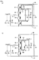
図1は、本発明の実施の形態1に従う電源システム5の構成を示す回路図である。
[Embodiment 1]
FIG. 1 is a circuit diagram showing a configuration of a
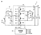
図1を参照して、電源システム5は、複数の直流電源10aおよび10bと、電力変換器50とを備える。電源システム5の負荷30は、電力線20および21の間に接続される。
Referring to FIG. 1,
本実施の形態において、直流電源10aおよび10bの各々は、リチウムイオン二次電池やニッケル水素電池のような二次電池、あるいは、電気二重層キャパシタやリチウムイオンキャパシタ等の出力特性に優れた直流電圧源要素により構成される。
In the present embodiment, each of
電力変換器50は、直流電源10aおよび10bと、電力線20および21との間に接続される。電力変換器50は、電力線20,21間の直流電圧(以下、出力電圧VHとも称する)を電圧指令値VH*に従って制御する。すなわち、電力線20,21は、直流電源10aおよび10bに対して共通に設けられる。
負荷30は、電力変換器50が電力線20,21間に出力する出力電圧VHを受けて動作する。電圧指令値VH*は、負荷30の動作に適した電圧に設定される。さらに、負荷30は、回生発電等によって、直流電源10a,10bの充電電力を発生可能に構成されてもよい。
The
図2は、負荷30の構成例を示す概略図である。
図2を参照して、負荷30は、たとえば電動車両の走行用電動機を含むように構成される。負荷30は、平滑キャパシタCHと、インバータ32と、モータジェネレータ35と、動力伝達ギヤ36と、駆動輪37とを含む。
FIG. 2 is a schematic diagram illustrating a configuration example of the
Referring to FIG. 2, load 30 is configured to include, for example, a traveling motor for an electric vehicle.
モータジェネレータ35は、車両駆動力を発生するための走行用電動機であり、たとえば、複数相の永久磁石型同期電動機で構成される。モータジェネレータ35の出力トルクは、減速機や動力分割機構によって構成される動力伝達ギヤ36を経由して、駆動輪37へ伝達される。駆動輪37に伝達されたトルクにより電動車両が走行する。また、モータジェネレータ35は、電動車両の回生制動時には、駆動輪37の回転力によって発電する。この発電電力は、インバータ32によってAC/DC変換される。この直流電力は、電源システム5に含まれる直流電源10a,10bの充電電力として用いることができる。
The
モータジェネレータの他にエンジン(図示せず)が搭載されたハイブリッド自動車では、このエンジンおよびモータジェネレータ35を協調的に動作させることによって、電動車両に必要な車両駆動力が発生される。この際には、エンジンの回転による発電電力を用いて直流電源10a,10bを充電することも可能である。
In a hybrid vehicle in which an engine (not shown) is mounted in addition to the motor generator, vehicle driving force required for the electric vehicle is generated by cooperatively operating the engine and the
このように、電動車両は、走行用電動機を搭載する車両を包括的に示すものであり、エンジンおよび電動機により車両駆動力を発生するハイブリッド自動車と、エンジンを搭載
しない電気自動車および燃料電池車との両方を含むものである。
As described above, the electric vehicle comprehensively represents a vehicle equipped with the electric motor for traveling, and includes a hybrid vehicle that generates vehicle driving force by the engine and the electric motor, and an electric vehicle and a fuel cell vehicle not equipped with the engine. It includes both.
負荷30(モータジェネレータ35)の動作は、電動車両の走行状態(代表的には車速)およびドライバ操作(代表的には、アクセルペダルおよびブレーキペダルの操作)に応じて、必要な車両駆動力または車両制動力が得られるように制御される。すなわち、負荷30の動作指令(たとえば、モータジェネレータ35のトルク指令値)は、電動車両の走行制御によって設定される。当該走行制御は、制御装置40(図1)とは別個の上位ECUによって実行されることが好ましい。 The operation of the load 30 (motor generator 35) depends on the driving state of the electric vehicle (typically the vehicle speed) and the driver operation (typically the operation of the accelerator pedal and the brake pedal) or the required vehicle driving force or Control is performed to obtain a vehicle braking force. That is, an operation command for load 30 (for example, a torque command value for motor generator 35) is set by running control of the electric vehicle. The travel control is preferably executed by a host ECU separate from the control device 40 (FIG. 1).
再び図1を参照して、平滑キャパシタCaは、リレー12aを経由して、直流電源10aと並列に接続される。同様に、平滑キャパシタCbは、リレー12bを経由して、直流電源10bと並列に接続される。リレー12aおよび12bは、電源システム5の起動時に、直流電源10a,10bのそれぞれを電力変換器50に接続する。
Referring to FIG. 1 again, smoothing capacitor Ca is connected in parallel with
直流電源10aのみに対して、電流制限回路13が配置される。電流制限回路13は、リレー12aに対して並列に接続される。電流制限回路13は、直列に接続されたリレー14および電流制限抵抗15を有する。リレー12aがオフされた状態で、リレー14のオンによって電流制限回路13を作動させることにより、電流制限抵抗15を経由した電流経路によって、平滑キャパシタCaを緩やかにプリチャージすることができる。
Current limiting
リレー12a,12b,14は、制御装置40からの制御信号(図示せず)に応答してオンオフされる。なお、電磁リレーや半導体リレー等のオンオフ制御可能な任意の開閉器を、リレー12a,12b,14として適用することができる。
電源システム5では、直流電源10aに対応して電流制限回路13が配置される一方で、直流電源10bおよび平滑キャパシタCbに対しては電流制限回路が配置されていない。このように、本実施の形態に従う電源システムでは、電流制限回路13は、全ての直流電源に対応して設けられるのではなく、一部の直流電源に対しては電流制限回路の配置が省略される点が特徴である。
In the
電力変換器50は、電力線20および21の間に直列に接続されたスイッチング素子S1〜S4と、リアクトルL1,L2とを含む。本実施の形態において、スイッチング素子としては、IGBT(Insulated Gate Bipolar Transistor)、電力用MOS(Metal Oxide Semiconductor)トランジスタあるいは電力用バイポーラトランジスタ等を用いることができる。スイッチング素子S1〜S4に対しては、逆並列ダイオードD1〜D4が配置されている。また、スイッチング素子S1〜S4は、制御信号SG1〜SG4にそれぞれ応答して、オンオフを制御することが可能である。すなわち、スイッチング素子S1〜S4は、制御信号SG1〜SG4がハイレベル(以下、Hレベル)のときにオンする一方で、ローレベル(以下、Lレベル)のときにオフする。
スイッチング素子S1は、電力線20およびノードN1の間に電気的に接続される。リアクトルL2は、ノードN1と直流電源10bの正極端子との間に接続される。スイッチング素子S2はノードN1およびN2の間に電気的に接続される。リアクトルL1はノードN2と直流電源10aの正極端子との間に接続される。リアクトルL2はノードN1と直流電源10bの正極端子との間に接続される。すなわち、ノードN1は、スイッチング素子S1およびS2の接続モードに対応し、ノードN2は、スイッチング素子S2およびS3の接続モードに対応する。
Switching element S1 is electrically connected between
スイッチング素子S3は、ノードN2およびN3の間に電気的に接続される。ノードN3は、直流電源10bの負極端子と電気的に接続される。スイッチング素子S4は、ノードN3および電力線21の間に電気的に接続される。電力線21は、負荷30および、直流電源10aの負極端子と電気的に接続される。すなわち、ノードN3は、スイッチング素子S3およびS4の接続モードに対応する。
Switching element S3 is electrically connected between nodes N2 and N3. Node N3 is electrically connected to the negative terminal of
図1から理解されるように、電力変換器50は、直流電源10aおよび直流電源10bの各々に対応して昇圧チョッパ回路を備えた構成となっている。すなわち、直流電源10aに対しては、スイッチング素子S1,S2を上アーム素子とする一方で、スイッチング素子S3,S4を下アーム素子とする電流双方向の第1の昇圧チョッパ回路が構成される。同様に、直流電源10bに対しては、スイッチング素子S1,S4を上アーム素子とする一方で、スイッチング素子S2,S3を下アーム素子とする電流双方向の第2の昇圧チョッパ回路が構成される。
As can be understood from FIG. 1, the
そして、第1の昇圧チョッパ回路によって、直流電源10aおよび電力線20の間に形成される電力変換経路と、第2の昇圧チョッパ回路によって、直流電源10bおよび電力線20の間に形成される電力変換経路との両方に、スイッチング素子S1〜S4が含まれる。
A power conversion path formed between the
制御装置40は、たとえば、図示しないCPU(Central Processing Unit)およびメモリを内蔵した電子制御ユニット(ECU)により構成されて、当該メモリに記憶されたマップおよびプログラムに基づいて、各センサによる検出値を用いた演算処理を行なうように構成される。あるいは、制御装置40の少なくとも一部は、電子回路等のハードウェアにより所定の数値・論理演算処理を実行するように構成されてもよい。
The
制御装置40は、負荷30への出力電圧VHを制御するために、スイッチング素子S1〜S4のオンオフを制御する制御信号SG1〜SG4を生成する。さらに、制御装置40は、リレー12a,12b,14のオンオフを制御する制御信号(図示せず)をさらに生成する。
The
電圧センサ41は、平滑キャパシタCaの電圧Vcaを検出する。電圧センサ42は、平滑キャパシタCbの電圧Vcaを検出する。電圧センサ43は、平滑キャパシタCHの電圧、すなわち、出力電圧VHを検出する。電圧センサ41〜43の検出値は、制御装置40へ与えられる。
The
なお、図1では図示を省略しているが、直流電源10aの電圧(以下、Vaと表記する)および電流(以下、Iaと表記する)、直流電源10bの電圧(以下、Vbと表記する)および電流(以下、Ibと表記する)、ならびに、出力電圧VHの検出器(電圧センサ,電流センサ)が設けられている。さらに、直流電源10aおよび10bの温度(以下、TaおよびTbと表記する)の検出器(温度センサ)についても配置することが好ましい。これらの検出器の出力は、制御装置40へ与えられる。
Although not shown in FIG. 1, the voltage (hereinafter referred to as Va) and current (hereinafter referred to as Ia) of the
図1の構成において、スイッチング素子S1〜S4は、「第1のスイッチング素子」〜「第4のスイッチング素子」にそれぞれ対応し、リアクトルL1およびL2は、「第1のリアクトル」および「第2のリアクトル」にそれぞれ対応する。また、リレー12a,12b,14は、「第1の開閉器」、「第2の開閉器」および「第3の開閉器」にそれぞれ対応する。
In the configuration of FIG. 1, switching elements S1 to S4 correspond to “first switching element” to “fourth switching element”, respectively, and reactors L1 and L2 correspond to “first reactor” and “second reactor”, respectively. Corresponds to "reactor" respectively. The
(起動後の電力変換器の動作)
電源システム5では、システム起動処理によって、平滑キャパシタCa,Cbを電圧Va,Vbまでプリチャージした後、リレー12a,12bをオンする一方で、リレー14をオフした状態で動作する。起動処理の詳細については、後程詳細に説明する。
(Operation of power converter after startup)
In the
電力変換器50は、直流電源10a,10bと電力線20との間での直流電力変換の態様が異なる複数の動作モードを有する。
The
図3には、電力変換器50が有する複数の動作モードが示される。
図3を参照して、動作モードは、スイッチング素子S1〜S4の周期的なオンオフ制御に伴って直流電源10aおよび/または10bの出力電圧を昇圧する「昇圧モード(B)」と、スイッチング素子S1〜S4のオンオフを固定して直流電源10aおよび/または10bを電力線20と電気的に接続する「直結モード(D)」とに大別される。
FIG. 3 shows a plurality of operation modes that the
Referring to FIG. 3, the operation mode includes “boost mode (B)” in which the output voltage of
昇圧モードには、直流電源10aおよび10bと電力線20との間で並列なDC/DC変換を行なう「パラレル昇圧モード(以下、PBモード)」と、直列接続された直流電源10aおよび10bと電力線20との間でDC/DC変換を行なう「シリーズ昇圧モード(以下、SBモード)」とが含まれる。PBモードは、特許文献1での「パラレル接続モード」に対応し、SBモードは、特許文献1での「シリーズ接続モード」に対応する。
In the boost mode, a “parallel boost mode (hereinafter referred to as PB mode)” in which DC / DC conversion is performed in parallel between DC power supplies 10 a and 10 b and
さらに、昇圧モードには、直流電源10aのみを用いて電力線20との間でDC/DC変換を行なう「直流電源10aによる単独モード(以下、aBモード)」と、直流電源10bのみを用いて電力線20との間でDC/DC変換を行なう「直流電源10bによる単独モード(以下、bBモード)」とが含まれる。aBモードでは、直流電源10bは、出力電圧VHが直流電源10bの電圧Vbよりも高く制御されている限りにおいて、電力線20と電気的に切り離された状態を維持されて不使用とされる。同様に、bBモードでは、直流電源10aは、出力電圧VHが直流電源10aの電圧Vaよりも高く制御されている限りにおいて、電力線20と電気的に切り離された状態を維持されて不使用とされる。
Further, in the boost mode, a “single mode by
昇圧モードに含まれる、PBモード、SBモード、aBモードおよびbBモードの各々では、電力線20の出力電圧VHは、電圧指令値VH*に従って制御される。これらの各モードにおけるスイッチング素子S1〜S4の制御については後述する。
In each of the PB mode, SB mode, aB mode, and bB mode included in the boost mode, output voltage VH of
直結モードには、直流電源10aおよび10bを電力線20に対して並列に接続した状態を維持する「並列直結モード(以下、PDモード)」と、直流電源10aおよび10bを電力線20に対して直列に接続した状態を維持する「シリーズ直結モード(以下、SDモード)」とが含まれる。
In the direct connection mode, the “parallel direct connection mode (hereinafter referred to as PD mode)” in which the DC power supplies 10 a and 10 b are connected in parallel to the
PDモードでは、スイッチング素子S1,S2,S4をオンに固定する一方で、スイッチング素子S3がオフに固定される。これにより、出力電圧VHは、直流電源10a,10bの出力電圧Va,Vb(厳密にはVa,Vbのうちの高い方の電圧)と同等となる。Va,Vb間の電圧差は直流電源10a,10bに短絡電流を生じさせるので、当該電圧差が小さいときに限定して、PDモードを適用することができる。
In the PD mode, the switching elements S1, S2, and S4 are fixed on, while the switching element S3 is fixed off. As a result, the output voltage VH becomes equal to the output voltages Va and Vb (strictly, the higher voltage of Va and Vb) of the
SDモードでは、スイッチング素子S2,S4がオフに固定される一方で、スイッチング素子S1,S3がオンに固定される。これにより、出力電圧VHは、直流電源10a,10bの出力電圧Va,Vbの和に従って一意に決まる(VH=Va+Vb)。
In the SD mode, the switching elements S2 and S4 are fixed off, while the switching elements S1 and S3 are fixed on. Thereby, the output voltage VH is uniquely determined according to the sum of the output voltages Va and Vb of the
さらに、直結モードには、直流電源10aのみを電力線20と電気的に接続する「直流電源10aの直結モード(以下、aDモード)」と、直流電源10bのみを電力線20と電気的に接続する「直流電源10bの直結モード(以下、bDモード)」とが含まれる。
Furthermore, in the direct connection mode, “direct connection mode of
aDモードでは、スイッチング素子S1,S2がオンに固定される一方で、スイッチング素子S3,S4がオフに固定される。これにより、直流電源10bは電力線20から切り離された状態となり、出力電圧VHは、直流電源10aの電圧Vaと同等となる(VH=Va)。aDモードでは、直流電源10bは、電力線20と電気的に切り離された状態を維持されて不使用とされる。なお、Vb>Vaの状態でaDモードを適用すると、スイッチング素子S2を介して直流電源10bから10aに短絡電流が生じる。このため、aDモードの適用には、Va>Vbが必要条件となる。
In the aD mode, the switching elements S1 and S2 are fixed on, while the switching elements S3 and S4 are fixed off. As a result, the
同様に、bDモードでは、スイッチング素子S1,S4がオンに固定される一方で、スイッチング素子S2,S3がオフに固定される。これにより、直流電源10aは電力線20から切り離された状態となり、出力電圧VHは、直流電源10bの電圧Vbと同等となる(VH=Vb)。bDモードでは、直流電源10aは、電力線20と電気的に切り離された状態を維持されて不使用とされる。なお、Va>Vbの状態でbDモードを適用すると、ダイオードD2を介して直流電源10aから10bに短絡電流が生じる。このため、bDモードの適用には、Vb>Vaが必要条件となる。
Similarly, in the bD mode, the switching elements S1 and S4 are fixed on, while the switching elements S2 and S3 are fixed off. As a result, the
直結モードに含まれる、PDモード、SDモード、aDモードおよびbDモードの各々では、電力線20の出力電圧VHは、直流電源10a,10bの電圧Va,Vbに依存して決まるため、直接制御することができなくなる。このため、直結モードに含まれる各モードでは、出力電圧VHが負荷30の動作に適した電圧に設定できなくなることにより、負荷30での電力損失が増加する可能性がある。
In each of the PD mode, SD mode, aD mode, and bD mode included in the direct connection mode, the output voltage VH of the
一方で、直結モードでは、スイッチング素子S1〜S4がオンオフされないため、電力変換器50の電力損失が大幅に抑制される。したがって、負荷30の動作状態によっては、直結モードの適用によって、負荷30の電力損失増加量よりも電力変換器50での電力損失減少量が多くなることにより、電源システム5全体での電力損失が抑制できる可能性がある。
On the other hand, in the direct connection mode, since the switching elements S1 to S4 are not turned on / off, the power loss of the
図3において、PBモードは「第1のモード」に対応し、SBモードは「第2のモード」に対応し、SDモードは「第3のモード」に対応する。さらに、aBモードおよびbBモードは「第4のモード」に対応し、aDモードおよびbDモードは「第5のモード」に対応し、PDモードは「第6のモード」に対応する。 In FIG. 3, the PB mode corresponds to a “first mode”, the SB mode corresponds to a “second mode”, and the SD mode corresponds to a “third mode”. Furthermore, the aB mode and the bB mode correspond to the “fourth mode”, the aD mode and the bD mode correspond to the “fifth mode”, and the PD mode corresponds to the “sixth mode”.
図4は、直流電源10a,10bを異なる種類の電源で構成した場合における両直流電源の特性の一例を示す概念図である。図4には、横軸にエネルギ、縦軸に電力をプロットした、いわゆるラゴンプロットが示される。一般的に、直流電源の出力パワーおよび蓄積エネルギはトレードオフの関係にあるため、高容量型のバッテリでは高出力を得ることが難しく、高出力型のバッテリでは蓄積エネルギを高めることが難しい。
FIG. 4 is a conceptual diagram showing an example of characteristics of both DC power supplies when the
したがって、直流電源10a,10bは、一方が、蓄積エネルギが高い、いわゆる高容量型の電源で構成されるのに対して、他方が、出力パワーが高い、いわゆる高出力型の電源で構成されることが好ましい。このようにすると、高容量型の電源に蓄積されたエネルギを平準的に長期間使用する一方で、高出力型の電源をバッファとして使用して、高容量型の電源による不足分を出力することができる。
Accordingly, one of the
図4の例では、直流電源10aが高容量型の電源で構成される一方で、直流電源10bは高出力型の電源で構成される。したがって、直流電源10aの動作領域110は、直流電源10bの動作領域120と比較して、出力可能な電力範囲が狭い。一方で、動作領域120は、動作領域110と比較して、蓄積可能なエネルギ範囲が狭い。
In the example of FIG. 4, the
負荷30の動作点101では、高パワーが短時間要求される。たとえば、電動車両では、動作点101は、ユーザのアクセル操作による急加速時に対応する。これに対して、負荷30の動作点102では、比較的低パワーが長時間要求される。たとえば、電動車両では、動作点102は、継続的な高速定常走行に対応する。
At the
動作点101に対しては、主に、高出力型の直流電源10bからの出力によって対応することができる。一方で、動作点102に対しては、主に、高容量型の直流電源10aからの出力によって対応することができる。これにより、電動車両では、高容量型のバッテリに蓄積されたエネルギを長時間に亘って使用することによって、電気エネルギによる走行距離を延ばすことができるとともに、ユーザのアクセル操作に対応した加速性能を速やかに確保することができる。
The
このように、種類および容量の異なる直流電源を組み合わせることにより、各直流電源の特性を活かして、システム全体で有効に蓄積エネルギを使用することができる。以下、本実施の形態では、直流電源10aが二次電池で構成され、直流電源10bがキャパシタによって構成される例を説明する。ただし、直流電源10a,10bの組み合わせはこの例に限定されるものではなく、同種および/または同容量の直流電源(蓄電装置)によって構成することも可能である。
In this way, by combining DC power sources having different types and capacities, the stored energy can be effectively used in the entire system by utilizing the characteristics of each DC power source. Hereinafter, in the present embodiment, an example in which the
また、直流電源がバッテリによって構成される場合には、低温時に出力特性が低下する可能性や、高温時に劣化進行を抑制するために充放電が制限される可能性がある。特に、電動車両では、搭載位置の差異によって、直流電源10a,10bの間に温度差が発生するケースも生じる。したがって、電源システム5では、直流電源10a,10bの動作状態(特に温度)に応じて、あるいは、上述したような負荷30の要求に応じて、いずれか一方の直流電源のみを使用した方が、効率的であるケースが存在する。上述したような、直流電源10a,10bの一方のみを使用するモード(aBモード,bBモード,aDモード,bDモード)を設けることによって、これらのケースに対応することができる。
In addition, when the DC power source is constituted by a battery, there is a possibility that output characteristics may be reduced at a low temperature, and charging / discharging may be limited to suppress the progress of deterioration at a high temperature. In particular, in an electric vehicle, a temperature difference may occur between the
このように、本実施の形態1に従う電源システム5では、直流電源10a,10bおよび/または負荷30の動作状態に応じて、電源システム5全体での効率が最適化されるように、図3に示した複数の動作モードの選択しながら動作することができる。
As described above, in
(電源システムの起動処理)。
電源システム5の起動時には、平滑キャパシタCa,Cb,CHの電圧Vca,Vcb,VHは0となっている。したがって、システム起動処理においては、過大電流を生じさせることなく、各平滑キャパシタCa,Cb,CHのプリチャージを完了することが必要である。
(Power system startup process).
When the
本実施の形態に従う電源システムでは、一部の直流電源(図1の例では、直流電源10a)のみに電流制限回路13が配置されている。したがって、電流制限回路が設けられていない平滑キャパシタCbをプリチャージするために、以下のようなプリチャージ制御が実行される。
In the power supply system according to the present embodiment, current limiting
図5は、実施の形態1に従う電源システムの起動時におけるプリチャージ制御の処理手順を説明するためのフローチャートである。プリチャージ制御は、制御装置40が、以下に説明する処理手順に従って、リレー12a,12b,14およびスイッチング素子S1〜S4のオンオフを制御することによって実現される。
FIG. 5 is a flowchart for illustrating a precharge control processing procedure when the power supply system according to the first embodiment is started. The precharge control is realized by the
図5を参照して、電源システム5の起動時に、制御装置40は、まずステップS100により、電流制限回路13によって、平滑キャパシタCaのプリチャージ(以下、単にCaプリチャージとも称する)を実行する。
Referring to FIG. 5, when
ステップS100によるCaプリチャージでは、リレー12a,12bがオフされる一方で、リレー14がオンされる。これにより、電流制限回路13が作動する。平滑キャパシタCaは、電流制限抵抗15を経由した電流経路によって、直流電源10aにより充電される。これにより、過大な突入電流が生じることを防止できる。平滑キャパシタCaの電圧Vcaが直流電源10aの電圧Vaまで上昇すると、Caプリチャージは完了する。
In the Ca precharge in step S100, the
Caプリチャージ時には、平滑キャパシタCHも、ダイオードD1,D2によって形成される電流経路により、直流電源10aによって充電される。すなわち、Caプリチャージでは、電流制限回路13からの電流によって、平滑キャパシタCaおよびCHが並列に充電される。したがって、Caプリチャージの完了時点において、VH=Vca=Vaである。
During the Ca precharge, the smoothing capacitor CH is also charged by the
制御装置40は、Caプリチャージが完了すると、ステップS150により、リレー14をオフするとともに、リレー12aをオンする。これにより、プリチャージ後の平滑キャパシタCaと直流電源10aとは、電流制限抵抗15を経由せずに電気的に接続される。
When the Ca precharge is completed, the
制御装置40は、さらに、ステップS200により、スイッチング素子S1〜S4の周期的なオンオフ制御(スイッチング制御)を伴って、平滑キャパシタCbのプリチャージ(以下、Cbプリチャージとも称する)を実行する。後述するように、Cbプリチャージでは、リレー12bがオフされた状態で、2つのプリチャージモードP1およびP2が順に選択される。
Further, in step S200,
制御装置40は、平滑キャパシタCbの電圧Vcbが直流電源10bの電圧Vbまで上昇すると、ステップS250により、Cbプリチャージを完了する。
When voltage Vcb of smoothing capacitor Cb rises to voltage Vb of
制御装置40は、Cbプリチャージが完了すると、ステップS300により、リレー12bをオンする。これにより、プリチャージ後の平滑キャパシタCaおよびCbの両方が、直流電源10aおよび10bとそれぞれ並列に接続された状態となって、起動処理が終了する。
When the Cb precharge is completed,
次に、Cbプリチャージの詳細について、さらに説明を進める。
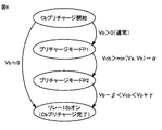
図6には、Cbプリチャージの状態遷移図が示される。
Next, the details of the Cb precharge will be further described.
FIG. 6 shows a state transition diagram of Cb precharge.
図6を参照して、Cbプリチャージが開始されると、直流電源10bの電圧Vbがまず判定される。電圧Vbがほぼ0であるときには、リレー12bをオンしても、直流電源10bおよび平滑キャパシタCbの間に大きな電流が流れるおそれがない。したがって、Vb≒0の場合には、Cbのプリチャージが開始されると、スイッチング制御によるプリチャージを省略して、直ちにCbプリチャージを完了して、リレー12bをオンすることができる。
Referring to FIG. 6, when Cb precharge is started, voltage Vb of
通常時には、直流電圧Vb>0であるから、Cbプリチャージが開始されると、プリチャージモードP1が選択される。そして、プリチャージモードP1により、平滑キャパシタCbの電圧Vcbが、電圧Va,Vbのうちの低い方の電圧min(Va,Vb)近傍まで上昇すると、プリチャージモードP1が終了されて、プリチャージモードP2が選択される。たとえば、電圧Vcbがmin(Va,Vb)−α(α:所定値)よりも高くなると、プリチャージモードP1が終了される。 Since the DC voltage Vb> 0 is normal, the precharge mode P1 is selected when the Cb precharge is started. When the voltage Vcb of the smoothing capacitor Cb rises to the vicinity of the lower voltage min (Va, Vb) of the voltages Va and Vb by the precharge mode P1, the precharge mode P1 is terminated and the precharge mode P2 is selected. For example, when voltage Vcb becomes higher than min (Va, Vb) −α (α: a predetermined value), precharge mode P1 is terminated.
さらに、平滑キャパシタCbの電圧Vcbが、直流電源10bの電圧Vb近傍になると、プリチャージモードP2が終了されて、Cbプリチャージが完了する。これにより、リレー12bのオンが可能となる。たとえば、電圧Vcbが、Vb−β<Vcb<Vb+γ(β,γ:所定値)の範囲内になると、プリチャージモードP2が終了される。
Further, when the voltage Vcb of the smoothing capacitor Cb becomes close to the voltage Vb of the
図7は、CbプリチャージにおけるプリチャージモードP1およびP2での回路動作を説明するための図表である。 FIG. 7 is a chart for explaining circuit operations in precharge modes P1 and P2 in Cb precharge.
図7を参照して、プリチャージモードP1,P2の各々では、デューティ比Dpに従う制御パルス信号SDpに従って、スイッチング素子S1〜S4のオンオフが制御される。 Referring to FIG. 7, in each of precharge modes P1 and P2, on / off of switching elements S1 to S4 is controlled according to control pulse signal SDp according to duty ratio Dp.
プリチャージモードP1では、制御パルス信号SDp,/SDpに従って、スイッチング素子S1およびS3のペアと、スイッチング素子S2およびS4のペアとが、相補的にオンオフされる。以下では、Vb>Vaであるときの動作例を説明する。 In the precharge mode P1, the pair of switching elements S1 and S3 and the pair of switching elements S2 and S4 are complementarily turned on and off according to the control pulse signals SDp and / SDp. Hereinafter, an operation example when Vb> Va is described.
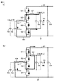
図8には、プリチャージモードP1における回路動作が示される。
図8(a)を参照して、スイッチング素子S2,S4がオンされる一方で、スイッチング素子S1,S3がオフされる期間では、平滑キャパシタCbが、リアクトルL1,L2を経由して直流電源10aに対して並列に接続される。この際に、平滑キャパシタCbを流れる電流の増加量は、リアクトルL1およびL2、ならびに、スイッチング素子S2,S4のオン期間の長さによって制限されるので、過大な電流は生じない。図8(a)の回路動作を継続すると、最終的にはVcb=Vaとなる。
FIG. 8 shows a circuit operation in the precharge mode P1.
Referring to FIG. 8A, in the period in which switching elements S2 and S4 are turned on while switching elements S1 and S3 are turned off, smoothing capacitor Cb is connected to
図8(b)を参照して、スイッチング素子S1,S3がオンされる一方で、スイッチング素子S2,S4がオフされる期間では、直流電源10aおよび平滑キャパシタCbは、リアクトルL1,L2を経由して、電力線20および21の間に直列に接続される。これにより、平滑キャパシタCHの電圧VHは、(Va+Vcb)へ向けて上昇する。この際にも、平滑キャパシタCbを流れる電流の増加量は、リアクトルL1およびL2、ならびに、スイッチング素子S1,S3のオン期間の長さによって制限される。
Referring to FIG. 8 (b), while switching elements S1 and S3 are turned on,
再び図8を参照して、プリチャージモードP1では、図8(a)および(b)の期間の比率を決めるデューティ比Dpは、下記(1)式に従って、0≦Dp<Dmax(Dmax<1)の範囲内で設定される。 Referring to FIG. 8 again, in the precharge mode P1, the duty ratio Dp for determining the ratio of the periods in FIGS. 8A and 8B is 0 ≦ Dp <Dmax (Dmax <1) according to the following equation (1). ).
Dp=(VH−Vcb)/VH …(1)
図9には、各プリチャージモードにおけるスイッチング制御でのデューティ比を設定するためのパルス幅変調制御を説明する概念的な波形図が示される。
Dp = (VH−Vcb) / VH (1)
FIG. 9 is a conceptual waveform diagram for explaining the pulse width modulation control for setting the duty ratio in the switching control in each precharge mode.
図9を参照して、デューティ比Dpと所定周期の搬送波CWとの電圧比較に基づいて、制御パルス信号SDpおよびその反転信号/SDpが生成される。搬送波CWの電圧がデューティ比Dpよりも大きい期間では、制御パルス信号SDpは、論理ローレベル(以下、Lレベルとも称する)に設定され、制御パルス信号/SDpは、論理ハイレベル(以下、単にHレベルとも称する)に設定される。 Referring to FIG. 9, control pulse signal SDp and its inverted signal / SDp are generated based on voltage comparison between duty ratio Dp and carrier wave CW having a predetermined period. In a period in which the voltage of the carrier wave CW is larger than the duty ratio Dp, the control pulse signal SDp is set to a logic low level (hereinafter also referred to as L level), and the control pulse signal / SDp is set to a logic high level (hereinafter simply referred to as H level). Level).
制御パルス信号SDpのLレベル期間では、図8(a)に示されるようにスイッチング素子S2,S4がオンされる一方で、制御パルス信号/SDpのLレベル期間では、図8(b)に示されるようにスイッチング素子S1,S3がオンされる。 In the L level period of the control pulse signal SDp, the switching elements S2 and S4 are turned on as shown in FIG. 8A. On the other hand, in the L level period of the control pulse signal / SDp, as shown in FIG. Thus, the switching elements S1 and S3 are turned on.
プリチャージモードP1の開始時には、VH=Vaである一方で、Vcb=0である。したがって、デューティ比Dpの初期値はDmaxとなる。Dmax<1のため、ごく短時間、図8(a)の回路動作が実行されることにより、Vcbが上昇する。以降では、Vcbの上昇に伴ってデューティ比Dpが低下することにより、図8(a)の回路動作の期間の比率が上昇する。そして、最終的には、Vcb=Vaとなった状態で、スイッチング動作が停止される。 At the start of the precharge mode P1, VH = Va while Vcb = 0. Therefore, the initial value of the duty ratio Dp is Dmax. Since Dmax <1, the circuit operation shown in FIG. 8A is executed for a very short time, whereby Vcb rises. Thereafter, the duty ratio Dp decreases as Vcb increases, so that the ratio of the circuit operation period of FIG. 8A increases. Finally, the switching operation is stopped in a state where Vcb = Va.
実際には、図6に示したように、Vcb>min(Va,Vb)−α(α:所定値)の条件が成立すると、プリチャージモードP1は終了される。プリチャージモードP1では、スイッチング素子S1,S4が同時にオンされないため、平滑キャパシタCHおよびCbの間に突入電流が流れることを防止できる。したがって、電圧Vcbが低い間には、プリチャージモードP1が適用される。 Actually, as shown in FIG. 6, when the condition of Vcb> min (Va, Vb) −α (α: predetermined value) is satisfied, the precharge mode P1 is terminated. In the precharge mode P1, since the switching elements S1 and S4 are not turned on at the same time, an inrush current can be prevented from flowing between the smoothing capacitors CH and Cb. Therefore, the precharge mode P1 is applied while the voltage Vcb is low.
再び、図7を参照して、プリチャージモードP2では、スイッチング素子S1,S4はオンに固定される一方で、制御パルス信号SDp,/SDpに従って、スイッチング素子S2とS3とが相補的にオンオフされる。 Referring to FIG. 7 again, in precharge mode P2, switching elements S1 and S4 are fixed on, while switching elements S2 and S3 are complementarily turned on and off according to control pulse signals SDp and / SDp. The
図10には、プリチャージモードP2における回路動作が示される。
図10(a)には、制御パルス信号/SDpのHレベル期間における回路動作が示される一方で、図10(b)には、制御パルス信号SDpのHレベル期間における回路動作が示される。
FIG. 10 shows a circuit operation in the precharge mode P2.
10A shows the circuit operation during the H level period of the control pulse signal / SDp, while FIG. 10B shows the circuit operation during the H level period of the control pulse signal SDp.
図10(a),(b)を通じて、スイッチング素子S1,S4がオンに維持されるので、プリチャージモードP2中には、平滑キャパシタCbおよびCHは、並列に接続された状態を維持する。 Since switching elements S1 and S4 are kept on through FIGS. 10A and 10B, smoothing capacitors Cb and CH remain connected in parallel during precharge mode P2.
一方で、図10(b)に示されたスイッチング素子S3,S4がオンされる期間と、図10(a)に示されたスイッチング素子S3がオフされる期間とを繰り返すことにより、いわゆる昇圧チョッパの回路動作によって、出力電圧VHが、直流電源10aの電圧Vaよりも昇圧される。すなわち、プリチャージモードP2では、並列接続された平滑キャパシタCbおよびCHを、直流電源10aの電圧Vaよりも高い電圧にプリチャージすることができる。
On the other hand, by repeating the period in which the switching elements S3 and S4 shown in FIG. 10B are turned on and the period in which the switching element S3 shown in FIG. With this circuit operation, the output voltage VH is boosted from the voltage Va of the
再び図7を参照して、プリチャージモードP2では、図10(a)および(b)の期間の比率を決めるデューティ比Dpは、下記(2)式に従って、0≦Dp<Dmax(Dmax<1)の範囲内で設定される。 Referring to FIG. 7 again, in the precharge mode P2, the duty ratio Dp for determining the ratio of the periods in FIGS. 10A and 10B is 0 ≦ Dp <Dmax (Dmax <1) according to the following equation (2). ).
Dp=(Vb−Vcb)/Vb …(2)
したがって、デューティ比Dpに基づく図9に示したパルス幅変調制御によって、VH*=Vcbを電圧指令値として出力電圧VHを制御するように、スイッチング素子S1〜S4のオンオフは制御される。そして、最終的には、VH=Vbとなった状態で、スイッチング動作が停止される。この結果、平滑キャパシタCHと並列に接続される平滑キャパシタCbについても、Vcb=Vbとなるまで、プリチャージすることが可能となる。
Dp = (Vb−Vcb) / Vb (2)
Therefore, on / off of the switching elements S1 to S4 is controlled by the pulse width modulation control shown in FIG. 9 based on the duty ratio Dp so as to control the output voltage VH using VH * = Vcb as a voltage command value. Finally, the switching operation is stopped in a state where VH = Vb. As a result, the smoothing capacitor Cb connected in parallel with the smoothing capacitor CH can be precharged until Vcb = Vb.
実際には、図6に示したように、Vb−β<Vcb<Vb+γ(β,γ:所定値)の条件が成立すると、プリチャージモードP2は終了されて、Cbプリチャージが完了する。 Actually, as shown in FIG. 6, when the condition of Vb−β <Vcb <Vb + γ (β, γ: predetermined value) is satisfied, the precharge mode P2 is ended and the Cb precharge is completed.
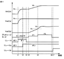
図11は、本実施の形態に従う電源システム5の起動処理におけるプリチャージ制御の第1の動作例を説明するための波形図である。図11には、上述したVb>Vaのときの動作例が示される。
FIG. 11 is a waveform diagram for describing a first operation example of precharge control in the startup process of
図11を参照して、電源システム5の起動が指示されると、時刻t1において、電流制限回路13のリレー14がオンされる。これにより、電流制限回路13が設けられた直流電源10aに対応する平滑キャパシタCaのプリチャージが開始される。
Referring to FIG. 11, when activation of
時刻t1より、電流制限抵抗15を経由した充電電流によって、平滑キャパシタCaおよびCHが充電される。この際には、電流制限抵抗15の作用によって、リレー14をオン状態に維持しても、過大な充電電流は発生しない。
From time t1, the smoothing capacitors Ca and CH are charged by the charging current via the current limiting
時刻t2において、平滑キャパシタCa,CHの電圧Vca,VHが、直流電源10aの電圧Vaと同等になると、Caプリチャージの完了に応じて、リレー12aがオンされる。さらに、時刻t3において、リレー14がオフされる。これにより、電流制限回路13は停止されて、電流制限抵抗15を経由せずに、直流電源10aおよび平滑キャパシタCaが電気的に接続される。
When the voltages Vca and VH of the smoothing capacitors Ca and CH become equal to the voltage Va of the
Caプリチャージの完了に応じて、Cbプリチャージが開始されると、まず、時刻t4から、プリチャージモードP1が開始される。プリチャージモードP1では、図7および図8で説明したスイッチング素子S1〜S4のオンオフ制御によって、スイッチング制御された電流によって平滑キャパシタCbが充電されることにより、電圧Vbが上昇する。電圧VHもVa+Vcbに従って上昇する。 When the Cb precharge is started in response to the completion of the Ca precharge, first, the precharge mode P1 is started from time t4. In the precharge mode P1, the smoothing capacitor Cb is charged by the switching-controlled current by the on / off control of the switching elements S1 to S4 described with reference to FIGS. 7 and 8, and the voltage Vb increases. The voltage VH also increases according to Va + Vcb.
図10の例では、min(Va,Vb)=Vaのため、時刻t5において、電圧VcbがVaまで上昇すると、プリチャージモードP1は終了されて、プリチャージモードP2が開始される。プリチャージモードP2では、図7および図9で説明したスイッチング素子S1〜S4のオンオフ制御によって、平滑キャパシタCbの電圧Vcbが、直流電源10aの電圧Vaよりも昇圧されて、電圧Vbへ向かって上昇する。電圧VHも同様に、電圧Vbへ向かって上昇する。
In the example of FIG. 10, since min (Va, Vb) = Va, when the voltage Vcb rises to Va at time t5, the precharge mode P1 is terminated and the precharge mode P2 is started. In the precharge mode P2, the voltage Vcb of the smoothing capacitor Cb is boosted from the voltage Va of the
時刻t6において、平滑キャパシタCbの電圧Vcbが、直流電源10bの電圧Vbとほぼ一致すると、プリチャージモードP2が終了されて、Cbプリチャージが完了する。これにより、時刻t7において、リレー12bがオンされる。
At time t6, when voltage Vcb of smoothing capacitor Cb substantially matches voltage Vb of
これにより、電源システム5の起動時におけるプリチャージ制御が完了する。この結果、直流電源10a,10bの各々は、リレー12a,12bを経由して、平滑キャパシタCa,Cbと並列接続された状態で、電力変換器50と接続される。すなわち、電源システム5は、起動時処理を終了して、図3に示された複数の動作モードのいずれかを適用して、出力電圧VHを電圧指令値VH*へ制御する動作を実行可能な状態となる。
Thereby, the precharge control at the time of starting of the
上述した起動時におけるプリチャージ制御は、直流電源10a,10bがVb<Vaの関係にある場合にも、同様に適用することができる。
The above-described precharge control at start-up can be similarly applied when the
図12は、本実施の形態に従う電源システム5の起動処理におけるプリチャージ制御の第2の動作例を説明するための波形図である。図12には、図11とは逆に、上述したVb<Vaのときの動作例が示される。
FIG. 12 is a waveform diagram for illustrating a second operation example of the precharge control in the startup process of
図12を参照して、時刻t1〜t3において、図11と同様にCaプリチャージが実行されるとともに、時刻t4からはプリチャージモードP1が開始される。これにより、スイッチング素子S1〜S4によりスイッチング制御された電流によって、平滑キャパシタCbが充電される。プリチャージモードP1では、平滑キャパシタCHの電圧VHは、電圧Vaからさらに上昇する。 Referring to FIG. 12, at time t1 to t3, Ca precharge is executed as in FIG. 11, and precharge mode P1 is started from time t4. As a result, the smoothing capacitor Cb is charged by the current whose switching is controlled by the switching elements S1 to S4. In the precharge mode P1, the voltage VH of the smoothing capacitor CH further increases from the voltage Va.
図12の例では、min(Va,Vb)=Vbのため、時刻t5において、電圧VcbがVbまで上昇すると、プリチャージモードP1は終了されて、プリチャージモードP2が開始される。しかしながら、プリチャージモードP2の開始時において、電圧Vcbは電圧Vb近傍まで上昇しているので、即座に、プリチャージモードP2の終了条件である、Vb−β<Vcb<Vb+γが、時刻t6において成立することになる。 In the example of FIG. 12, since min (Va, Vb) = Vb, when the voltage Vcb rises to Vb at time t5, the precharge mode P1 is terminated and the precharge mode P2 is started. However, since the voltage Vcb has increased to the vicinity of the voltage Vb at the start of the precharge mode P2, Vb−β <Vcb <Vb + γ, which is an end condition of the precharge mode P2, is immediately established at time t6. Will do.
この結果、Cbプリチャージが完了するので、時刻t7において、リレー12bがオンされる。すなわち、プリチャージモードP2はごく短期間で終了されて、電源システム5の起動時におけるプリチャージ制御が完了する。時刻t7以降では、図11の場合と同様に、直流電源10a,10bの各々は、リレー12a,12bを経由して、平滑キャパシタCa,Cbと並列接続された状態で、電力変換器50と接続される。
As a result, the Cb precharge is completed, so that
図11および図12に示したように、直流電源10a,10bの電圧Va,Vbの高低に関わらず、電流制限抵抗が設けられていない平滑キャパシタCbを電圧Vbへプリチャージすることができる。
As shown in FIGS. 11 and 12, the smoothing capacitor Cb in which the current limiting resistor is not provided can be precharged to the voltage Vb regardless of the levels of the voltages Va and Vb of the
このように、実施の形態1に従う電源システムでは、直流電源10aのみに電流制限回路13が配置されている構成としても、スイッチング素子S1〜S4によってスイッチング制御された電流によって、電流制限抵抗が設けられていない平滑キャパシタCbを充電することができる。この結果、直流電源の個数よりも電流制限回路の配置個数を少なくした回路構成によって、電源システムの起動時に、過大な突入電流を生じさせることなく、各平滑キャパシタをプリチャージすることができる。これにより、電源システムの部品点数削減による小型化および低コスト化を図ることができる。
Thus, in the power supply system according to the first embodiment, even if the current limiting
[実施の形態2]
実施の形態1では、直流電源10bに対応する電流制限回路13の配置を省略する構成を説明した。実施の形態2では、実施の形態1とは反対に、直流電源10aに対する電流制限回路13の配置を省略した構成における起動時制御について説明する。
[Embodiment 2]
In the first embodiment, the configuration is described in which the arrangement of the current limiting
図13は、本実施の形態2に従う電源システム5♯の構成を示す回路図である。
図13を図1と比較して、実施の形態2に従う電源システム5♯では、電流制限回路13が、リレー12bと並列に接続されている。一方で、直流電源10aのリレー12aに対しては、電流制限回路13が配置されていない。電源システム5♯のその他の部分の構成は、図1に示された電源システム5と同様であるので、詳細な説明は繰返さない。
FIG. 13 is a circuit diagram showing a configuration of
13 is compared with FIG. 1, in
実施の形態2に従う電源システムでは、直流電源10bのみに電流制限回路13が配置されているので、電流制限回路が設けられていない平滑キャパシタCaをプリチャージするために、以下のようなプリチャージ制御が実行される。
In the power supply system according to the second embodiment, since current limiting
図14は、実施の形態2に従う電源システムの起動時におけるプリチャージ制御の処理手順を説明するためのフローチャートである。プリチャージ制御は、制御装置40が、以下に説明する処理手順に従って、リレー12a,12b,14およびスイッチング素子S1〜S4のオンオフを制御することによって実現される。
FIG. 14 is a flowchart for illustrating the precharge control processing procedure when the power supply system according to the second embodiment is started. The precharge control is realized by the
図14を参照して、電源システム5♯の起動時に、制御装置40は、まずステップS100♯により、電流制限回路13によって、平滑キャパシタCbのプリチャージ(Cbプリチャージ)を実行する。
Referring to FIG. 14, when
ステップS100♯によるCbプリチャージでは、リレー12a,12bがオフされる一方で、リレー14がオンされる。これにより、電流制限回路13が作動する。平滑キャパシタCbは、電流制限抵抗15を経由した電流経路によって、直流電源10bにより充電される。これにより、過大な突入電流が生じることを防止できる。平滑キャパシタCbの電圧Vcbが直流電源10bの電圧Vbまで上昇すると、Cbプリチャージは完了する。
In the Cb precharge at step S100 #, relays 12a and 12b are turned off while
Cbプリチャージ時には、平滑キャパシタCHも、ダイオードD1,D2によって形成される電流経路により、直流電源10bによって充電される。すなわち、Cbプリチャージでは、電流制限回路13からの電流によって、平滑キャパシタCbおよびCHが並列に充電される。したがって、Cbプリチャージの完了時点において、VH=Vcb=Vbである。
During the Cb precharge, the smoothing capacitor CH is also charged by the
制御装置40は、Cbプリチャージが完了すると、ステップS150♯により、リレー14をオフするとともに、リレー12bをオンする。これにより、プリチャージ後の平滑キャパシタCbと直流電源10bとは、電流制限抵抗15を経由せずに電気的に接続される。
When the Cb precharge is completed,
制御装置40は、さらに、ステップS200♯により、スイッチング素子S1〜S4の周期的なオンオフ制御(スイッチング制御)を伴って、平滑キャパシタCaのプリチャージ(Caプリチャージ)を実行する。Caプリチャージでは、リレー12aがオフされた状態で、2つのプリチャージモードP1およびP2が順に選択される。
Further, in step S200 #,
制御装置40は、平滑キャパシタCaの電圧Vcaが直流電源10aの電圧Vaまで上昇すると、ステップS250♯により、Caプリチャージを完了する。
When voltage Vca of smoothing capacitor Ca rises to voltage Va of
制御装置40は、Caプリチャージが完了すると、ステップS300♯により、リレー12aをオンする。これにより、プリチャージ後の平滑キャパシタCaおよびCbの両方が、直流電源10aおよび10bとそれぞれ並列に接続された状態となって、起動処理が終了する。
When Ca precharge is completed,
次に、Caプリチャージの詳細について、さらに説明を進める。
図15には、Caプリチャージの状態遷移図が示される。
Next, the details of the Ca precharge will be further described.
FIG. 15 shows a state transition diagram of Ca precharge.
図15を参照して、Caプリチャージが開始されると、直流電源10aの電圧Vbがまず判定される。電圧Vaがほぼ0であるときには、スイッチング制御によるプリチャージを省略して、直ちにCaプリチャージを完了して、リレー12aをオンすることができる。
Referring to FIG. 15, when Ca precharge is started, voltage Vb of
通常時には、直流電圧Va>0であるから、Caプリチャージが開始されると、プリチャージモードP1が選択される。そして、プリチャージモードP1により、平滑キャパシタCaの電圧Vcaが、電圧Va,Vbのうちの低い方の電圧min(Va,Vb)近傍まで上昇すると、プリチャージモードP1が終了されて、プリチャージモードP2が選択される。たとえば、電圧Vcaがmin(Va,Vb)−α(α:所定値)よりも高くなると、プリチャージモードP1が終了される。 Since the DC voltage Va> 0 is normal, the precharge mode P1 is selected when the Ca precharge is started. Then, when the voltage Vca of the smoothing capacitor Ca rises to the vicinity of the lower voltage min (Va, Vb) of the voltages Va, Vb by the precharge mode P1, the precharge mode P1 is terminated, and the precharge mode P2 is selected. For example, when the voltage Vca becomes higher than min (Va, Vb) −α (α: a predetermined value), the precharge mode P1 is terminated.
さらに、平滑キャパシタCaの電圧Vcaが、直流電源10aの電圧Va近傍になると、プリチャージモードP2が終了されて、Caプリチャージが完了する。これにより、リレー12aのオンが可能となる。たとえば、電圧Vcaが、Va−β<Vca<Va+γ(β,γ:所定値)の範囲内になると、プリチャージモードP2が終了される。
Further, when the voltage Vca of the smoothing capacitor Ca becomes close to the voltage Va of the
図16は、CaプリチャージにおけるプリチャージモードP1およびP2での回路動作を説明するための図表である。 FIG. 16 is a chart for explaining circuit operations in precharge modes P1 and P2 in Ca precharge.
図16を参照して、Cbプリチャージと同様に、プリチャージモードP1,P2の各々では、デューティ比Dpに従う制御パルス信号SDpに従って、スイッチング素子S1〜S4のオンオフが制御される。 Referring to FIG. 16, similarly to Cb precharge, in each of precharge modes P1 and P2, on / off of switching elements S1 to S4 is controlled according to control pulse signal SDp according to duty ratio Dp.
プリチャージモードP1では、制御パルス信号SDp,/SDpに従って、スイッチング素子S1およびS3のペアと、スイッチング素子S2およびS4のペアとが、相補的にオンオフされる。以下では、Vb>Vaであるときの動作例を説明する。 In the precharge mode P1, the pair of switching elements S1 and S3 and the pair of switching elements S2 and S4 are complementarily turned on and off according to the control pulse signals SDp and / SDp. Hereinafter, an operation example when Vb> Va is described.
図17には、CaプリチャージのプリチャージモードP1における回路動作が示される。 FIG. 17 shows a circuit operation in the precharge mode P1 of Ca precharge.
図17(a)を参照して、スイッチング素子S2,S4がオンされる一方で、スイッチング素子S1,S3がオフされる期間では、平滑キャパシタCaが、リアクトルL1,L2を経由して直流電源10bに対して並列に接続される。この際に、平滑キャパシタCaを流れる電流の増加量は、リアクトルL1およびL2、ならびに、スイッチング素子S2,S4のオン期間の長さによって制限されるので、過大な電流は生じない。図17(a)の回路動作を継続すると、最終的にはVca=Vbとなる。
Referring to FIG. 17A, in the period in which switching elements S2 and S4 are turned on while switching elements S1 and S3 are turned off, smoothing capacitor Ca is connected to
図17(b)を参照して、スイッチング素子S1,S3がオンされる一方で、スイッチング素子S2,S4がオフされる期間では、直流電源10bおよび平滑キャパシタCaは、リアクトルL1,L2を経由して、電力線20および21の間に直列に接続される。これにより、平滑キャパシタCHの電圧VHは、(Vb+Vca)へ向けて上昇する。この際にも、平滑キャパシタCbを流れる電流の変化は、リアクトルL1およびL2、ならびに、スイッチング素子S1,S3のオン期間の長さによって制限される。
Referring to FIG. 17B, in a period in which switching elements S1 and S3 are turned on while switching elements S2 and S4 are turned off,
再び図16を参照して、CaプリチャージのプリチャージモードP1では、図17(a)および(b)の期間の比率を決めるデューティ比Dpは、下記(3)式に従って、0≦Dp<Dmax(Dmax<1)の範囲内で設定される。 Referring to FIG. 16 again, in the Ca precharge precharge mode P1, the duty ratio Dp for determining the ratio of the periods of FIGS. 17A and 17B is 0 ≦ Dp <Dmax according to the following equation (3): It is set within the range of (Dmax <1).
Dp=(VH−Vca)/VH …(3)
図9で説明したように、デューティ比Dpが低下すると制御パルス信号/SDpのHレベル期間が長くなるので、図17(a)に示されるようにスイッチング素子S2,S4がオンされる期間が長くなる。
Dp = (VH−Vca) / VH (3)
As described with reference to FIG. 9, when the duty ratio Dp decreases, the H level period of the control pulse signal / SDp becomes longer, so that the period during which the switching elements S2 and S4 are turned on becomes longer as shown in FIG. Become.
プリチャージモードP1の開始時には、デューティ比Dpの初期値はDmaxとなるので、ごく短時間、図17(a)の回路動作が実行されることにより、Vcaが上昇する。以降では、Vcaの上昇に伴ってデューティ比Dpが低下することにより、図17(a)の回路動作の期間の比率が上昇する。そして、図15に示したように、Vca>min(Va,Vb)−α(α:所定値)の条件が成立すると、プリチャージモードP1は終了される。 Since the initial value of the duty ratio Dp is Dmax at the start of the precharge mode P1, Vca rises by executing the circuit operation of FIG. 17A for a very short time. Thereafter, the duty ratio Dp decreases as Vca increases, so that the ratio of the circuit operation period of FIG. 17A increases. As shown in FIG. 15, when the condition of Vca> min (Va, Vb) −α (α: predetermined value) is satisfied, the precharge mode P1 is terminated.
再び、図16を参照して、プリチャージモードP2では、スイッチング素子S1,S2はオンに固定される一方で、制御パルス信号SDp,/SDpに従って、スイッチング素子S3およびS4が相補的にオンオフされる。 Referring to FIG. 16 again, in precharge mode P2, switching elements S1 and S2 are fixed on, while switching elements S3 and S4 are complementarily turned on and off according to control pulse signals SDp and / SDp. .
図18には、プリチャージモードP2における回路動作が示される。
図18(a)には、制御パルス信号/SDpのHレベル期間における回路動作が示される一方で、図18(b)には、制御パルス信号SDpのHレベル期間における回路動作が示される。
FIG. 18 shows a circuit operation in the precharge mode P2.
FIG. 18A shows the circuit operation in the H level period of the control pulse signal / SDp, while FIG. 18B shows the circuit operation in the H level period of the control pulse signal SDp.
図18(a),(b)を通じて、スイッチング素子S1,S2がオンに維持されるので、プリチャージモードP2中には、平滑キャパシタCaおよびCHは、並列に接続された状態を維持する。 Since switching elements S1 and S2 are kept on through FIGS. 18A and 18B, smoothing capacitors Ca and CH remain connected in parallel during precharge mode P2.
一方で、図18(b)に示されたスイッチング素子S2,S3がオンされる期間と、図18(a)に示されたスイッチング素子S3がオフされる期間とを繰り返すことにより、いわゆる昇圧チョッパの回路動作によって、出力電圧VHが、直流電源10bの電圧Vbよりも昇圧される。すなわち、プリチャージモードP2では、並列接続された平滑キャパシタCaおよびCHを、直流電源10bの電圧Vbよりも高い電圧にプリチャージすることができる。
On the other hand, by repeating the period in which the switching elements S2 and S3 shown in FIG. 18B are turned on and the period in which the switching element S3 shown in FIG. With this circuit operation, the output voltage VH is boosted above the voltage Vb of the
再び図16を参照して、プリチャージモードP2では、図18(a)および(b)の期間の比率を決めるデューティ比Dpは、下記(4)式に従って、0≦Dp<Dmax(Dmax<1)の範囲内で設定される。 Referring to FIG. 16 again, in the precharge mode P2, the duty ratio Dp for determining the ratio of the periods in FIGS. 18A and 18B is 0 ≦ Dp <Dmax (Dmax <1) according to the following equation (4). ).
Dp=(Va−Vca)/Va …(4)
したがって、デューティ比Dpに基づくパルス幅変調制御(図9)によって、VH*=Vcaを電圧指令値として出力電圧VHを制御するように、スイッチング素子S1〜S4のオンオフは制御される。そして、最終的には、VH=Vaとなった状態で、スイッチング動作が停止される。この結果、平滑キャパシタCHと並列に接続される平滑キャパシタCaについても、Vca=Vaとなるまで、プリチャージすることが可能となる。実際には、図15に示したように、Va−β<Vca<Va+γ(β,γ:所定値)の条件が成立すると、プリチャージモードP2は終了されて、Caプリチャージが完了する。
Dp = (Va−Vca) / Va (4)
Therefore, on / off of the switching elements S1 to S4 is controlled by pulse width modulation control (FIG. 9) based on the duty ratio Dp so as to control the output voltage VH using VH * = Vca as a voltage command value. Finally, the switching operation is stopped in a state where VH = Va. As a result, the smoothing capacitor Ca connected in parallel with the smoothing capacitor CH can be precharged until Vca = Va. Actually, as shown in FIG. 15, when the condition Va−β <Vca <Va + γ (β, γ: predetermined value) is satisfied, the precharge mode P2 is terminated and the Ca precharge is completed.
なお、Va>Vbの場合には、図11の動作波形図における電圧Vcaの挙動と同様に、電圧Vcbを制御することができる。すなわち、図11において、リレー12aとリレー12bとの波形図を入替えることにより、平滑キャパシタCaをプリチャージすることができる。
When Va> Vb, the voltage Vcb can be controlled similarly to the behavior of the voltage Vca in the operation waveform diagram of FIG. That is, in FIG. 11, the smoothing capacitor Ca can be precharged by switching the waveform diagrams of the
同様に、Vb>Vaの場合には、図12の動作波形図における電圧Vcaの挙動と同様に、電圧Vcbを制御することができる。すなわち、図12において、リレー12aとリレー12bとの波形図を入替えることにより、平滑キャパシタCaをプリチャージすることができる。
Similarly, when Vb> Va, the voltage Vcb can be controlled similarly to the behavior of the voltage Vca in the operation waveform diagram of FIG. That is, in FIG. 12, the smoothing capacitor Ca can be precharged by switching the waveform diagrams of the
このように、実施の形態2に従う電源システムでは、直流電源10bのみに電流制限回路13が配置されている構成としても、スイッチング素子S1〜S4によってスイッチング制御された電流によって、電流制限抵抗が設けられていない平滑キャパシタCaを充電することができる。この結果、直流電源の個数よりも電流制限回路の配置個数を少なくした回路構成によって、電源システムの起動時に、過大な突入電流を生じさせることなく、各平滑キャパシタをプリチャージすることができる。これにより、電源システムの部品点数削減による小型化および低コスト化を図ることができる。
Thus, in the power supply system according to the second embodiment, even if the current limiting
なお、電源システム5,5♯において、負荷30は、電力変換器によって制御される直流電圧によって動作する機器であれば、任意の機器によって構成できる点について確認的に記載する。すなわち、本実施の形態では、電動車両の走行用電動機を含むように負荷30が構成される例を説明したが、本発明の適用はこのような負荷に限定されるものではない。
In
今回開示された実施の形態はすべての点で例示であって制限的なものではないと考えられるべきである。本発明の範囲は上記した説明ではなくて特許請求の範囲によって示され、特許請求の範囲と均等の意味および範囲内でのすべての変更が含まれることが意図される。 The embodiment disclosed this time should be considered as illustrative in all points and not restrictive. The scope of the present invention is defined by the terms of the claims, rather than the description above, and is intended to include any modifications within the scope and meaning equivalent to the terms of the claims.
5,5♯ 電源システム、10a,10b 直流電源、12a,12b,14 リレー、13 電流制限回路、15 電流制限抵抗、20,21 電力線、30 負荷、32 インバータ、35 モータジェネレータ、36 動力伝達ギヤ、37 駆動輪、40 制御装置、41〜43 電圧センサ、50 電力変換器、101,102 動作点、110,120 動作領域、CH,Ca,Cb 平滑キャパシタ、CW 搬送波、D1〜D4 逆並列ダイオード、Dp デューティ比(プリチャージ制御、L1,L2 リアクトル、N1,N2,N3 ノード、S1〜S4 電力用半導体スイッチング素子、SDp,/SDp 制御パルス信号、SG1〜SG4 制御信号、VH 出力電圧、VH* 電圧指令値。 5, 5 # power supply system, 10a, 10b DC power supply, 12a, 12b, 14 relay, 13 current limiting circuit, 15 current limiting resistor, 20, 21 power line, 30 load, 32 inverter, 35 motor generator, 36 power transmission gear, 37 Drive wheel, 40 control device, 41-43 voltage sensor, 50 power converter, 101, 102 operating point, 110, 120 operating region, CH, Ca, Cb smoothing capacitor, CW carrier wave, D1-D4 anti-parallel diode, Dp Duty ratio (precharge control, L1, L2 reactor, N1, N2, N3 nodes, S1-S4 power semiconductor switching element, SDp, / SDp control pulse signal, SG1-SG4 control signal, VH output voltage, VH * voltage command value.
Claims (6)
第1の直流電源と、
第2の直流電源と、
前記第1の直流電源に対応する第1の開閉器と、
前記第2の直流電源に対応する第2の開閉器と、
前記第1の開閉器を経由して前記第1の直流電源と並列に接続された第1のキャパシタと、
前記第2の開閉器を経由して前記第2の直流電源と並列に接続された第2のキャパシタと、
前記第1および第2の電力線の間に電気的に接続された第3のキャパシタと、
前記第1および第2の電力線の間に順に直列接続された、第1から第4のスイッチング素子と、
前記第2および第3のスイッチング素子の接続ノードと、前記第1の直流電源の正極端子との間に電気的に接続された第1のリアクトルと、
前記第1および第2のスイッチング素子の接続ノードと、前記第2の直流電源の正極端子との間に電気的に接続された第2のリアクトルとを備え、
前記第1の直流電源の負極端子は、前記第2の電力線と電気的に接続され、
前記第2の直流電源の負極端子は、前記第3および第4のスイッチング素子の接続ノードと電気的に接続され、さらに、
前記第1および第2の直流電源のうちの一方の直流電源のみに対応して設けられ、前記第1および第2の開閉器のうちの対応する一方の開閉器に対して並列に接続された電流制限回路と、
前記第1から第4のスイッチング素子のオンオフおよび前記第1から第3の開閉器のオンオフを制御するための制御装置とを備え、
前記電流制限回路は、直列に接続された第3の開閉器および電流制限抵抗を有し、
前記制御装置は、
前記電源システムの起動時において、前記第1および第2の開閉器がオフされた状態で前記第3の開閉器をオンすることにより、前記第1および第2のキャパシタのうちの前記第3の開閉器と接続された一方のキャパシタおよび前記第3のキャパシタを前記一方の直流電源の出力電圧へプリチャージするための第1のプリチャージ手段と、
前記一方のキャパシタのプリチャージ完了に応じて、前記第3の開閉器をオフする一方で前記第1および第2の開閉器のうちの前記一方の開閉器をオンするための手段と、
前記一方の開閉器がオンされる一方で、前記第1および第2の開閉器のうちの他方の開閉器と前記第3の開閉器とがオフされている状態で、前記第1および第2のキャパシタのうちの他方のキャパシタを、前記第1および第4のスイッチング素子の周期的なオンオフ制御を伴って前記第1および第2の直流電源のうちの他方の直流電源の出力電圧へプリチャージするための第2のプリチャージ手段と、
前記他方のキャパシタのプリチャージ完了に応じて、前記他方の開閉器をオンするための手段とを含む、電源システム。 A power supply system for outputting a DC voltage between first and second power lines connected to a load,
A first DC power supply;
A second DC power source;
A first switch corresponding to the first DC power supply;
A second switch corresponding to the second DC power supply;
A first capacitor connected in parallel with the first DC power source via the first switch;
A second capacitor connected in parallel with the second DC power source via the second switch;
A third capacitor electrically connected between the first and second power lines;
First to fourth switching elements sequentially connected in series between the first and second power lines;
A first reactor electrically connected between a connection node of the second and third switching elements and a positive terminal of the first DC power supply;
A second reactor electrically connected between a connection node of the first and second switching elements and a positive terminal of the second DC power supply;
A negative terminal of the first DC power supply is electrically connected to the second power line;
A negative terminal of the second DC power supply is electrically connected to a connection node of the third and fourth switching elements;
Provided corresponding to only one of the first and second DC power supplies, and connected in parallel to the corresponding one of the first and second switches A current limiting circuit;
A controller for controlling on / off of the first to fourth switching elements and on / off of the first to third switches;
The current limiting circuit has a third switch and a current limiting resistor connected in series,
The controller is
When the power supply system is activated, the third switch of the first and second capacitors is turned on by turning on the third switch while the first and second switches are turned off. First precharging means for precharging one capacitor connected to the switch and the third capacitor to an output voltage of the one DC power supply;
Means for turning on one of the first and second switches while turning off the third switch in response to completion of precharging of the one capacitor;
While the one switch is turned on, the first and second switches are turned off while the other switch of the first and second switches and the third switch are turned off. The other capacitor is precharged to the output voltage of the other DC power source among the first and second DC power sources with periodic on / off control of the first and fourth switching elements. Second precharging means for
Means for turning on the other switch in response to completion of precharging of the other capacitor.
前記他方のキャパシタおよび前記第3のキャパシタの電圧を、前記第1および第2の直流電源のそれぞれの出力電圧のうちの低い方の電圧まで上昇させるように、前記第1からの第4のスイッチング素子を周期的にオンオフ制御するための第1のスイッチング制御手段と、
前記他方のキャパシタの電圧が前記低い方の電圧まで上昇した後に、前記他方のキャパシタおよび前記第3のキャパシタの電圧を、前記他方の直流電源の出力電圧まで上昇させるように、前記第1からの第4のスイッチング素子を周期的にオンオフ制御するための第2のスイッチング制御手段とを有する、請求項1記載の電源システム。 The second precharge means includes
The fourth switching from the first so as to increase the voltage of the other capacitor and the third capacitor to the lower one of the output voltages of the first and second DC power supplies. First switching control means for periodically turning on and off the element;
After the voltage of the other capacitor rises to the lower voltage, the voltage of the other capacitor and the third capacitor is increased to the output voltage of the other DC power source, The power supply system according to claim 1, further comprising second switching control means for periodically turning on and off the fourth switching element.
前記他方のキャパシタの電圧が前記低い方の電圧に上昇するまでの間、前記他方のキャパシタを前記第1および第2のリアクトルを経由して前記一方の直流電源に対して並列に接続する第1の動作と、前記一方の直流電源および前記他方のキャパシタを直列に前記第1および第2のリアクトルを経由して前記第1および第2の電力線の間に電気的に接続する第2の動作とを周期的に繰り返すように、前記第1からの第4のスイッチング素子の周期的なオンオフを制御するための手段を有する、請求項2記載の電源システム。 The first switching control means includes:
The first capacitor is connected in parallel to the one DC power source via the first and second reactors until the voltage of the other capacitor rises to the lower voltage. And the second operation of electrically connecting the one DC power source and the other capacitor in series between the first and second power lines via the first and second reactors. 3. The power supply system according to claim 2, further comprising means for controlling periodic on / off of the first to fourth switching elements so as to periodically repeat.
前記他方のキャパシタの電圧が前記他方の直流電源の出力電圧へ上昇するまでの間、前記一方の直流電源および前記第1または第2のリアクトルによる電流循環経路を形成する第3の動作と、前記一方の直流電源および前記第1または第2のリアクトルを直列に前記第1および第2の電力線の間に電気的に接続する第4の動作とを周期的に繰り返すように、前記第1からの第4のスイッチング素子の周期的なオンオフを制御するための手段を有する、請求項2記載の電源システム。 The second switching control means includes:
A third operation for forming a current circulation path by the one DC power source and the first or second reactor until the voltage of the other capacitor rises to the output voltage of the other DC power source; From the first to the first DC power supply and the fourth operation of electrically connecting the first or second reactor in series between the first and second power lines to periodically repeat The power supply system according to claim 2, comprising means for controlling periodic on / off of the fourth switching element.
前記複数の動作モードは、
前記第1から第4のスイッチング素子のオンオフ制御によって、前記第1および第2の直流電源が前記第1および第2の電力線との間で並列に直流電圧変換を実行する第1のモードと、
前記第3のスイッチング素子をオン固定するとともに前記第1、第2および第4のスイッチング素子をオンオフ制御することによって、前記第1および前記第2の直流電源が直列接続された状態で前記第1および第2の電力線との間で直流電圧変換を実行する第2のモードと、
前記第1から第4のスイッチング素子のオンオフを固定して、前記第1および第2の電力線に対して前記第1および第2の直流電源が直列に接続された状態を維持する第3のモードと、
前記第1から第4のスイッチング素子のオンオフ制御によって、前記第1および第2の直流電源の一方の直流電源と前記第1および第2の電力線との間で直流電圧変換を実行する第4のモードと、
前記第1から第4のスイッチング素子のオンオフを固定して、前記第1および第2の直流電源の一方が前記第1および第2の電力線に電気的に接続される一方で、前記第1および第2の直流電源の他方が前記第1および第2の電力線から電気的に切り離された状態を維持する第5のモードと、
前記第1から第4のスイッチング素子のオンオフを固定して、前記第1および第2の電力線に対して前記第1および第2の直流電源が並列に接続された状態を維持する第6のモードとを含む、請求項1〜5のいずれか1項に記載の電源システム。 The power supply system controls the DC voltage by selectively operating one of the plurality of operation modes in a state where the first and second switches are turned on. Composed of
The plurality of operation modes are:
A first mode in which the first and second DC power supplies perform DC voltage conversion in parallel with the first and second power lines by ON / OFF control of the first to fourth switching elements;
The first and second DC power supplies are connected in series by fixing the third switching element on and controlling the first, second and fourth switching elements on and off. And a second mode for performing DC voltage conversion with the second power line;
A third mode in which the first to fourth switching elements are fixed on and off and the first and second DC power supplies are connected in series to the first and second power lines. When,
A fourth voltage that performs DC voltage conversion between one DC power source of the first and second DC power sources and the first and second power lines by on / off control of the first to fourth switching elements. Mode,
On and off of the first to fourth switching elements are fixed, and one of the first and second DC power supplies is electrically connected to the first and second power lines, while the first and second A fifth mode in which the other of the second DC power supplies is kept electrically disconnected from the first and second power lines;
A sixth mode in which ON / OFF of the first to fourth switching elements is fixed and the first and second DC power supplies are connected in parallel to the first and second power lines. The power supply system of any one of Claims 1-5 containing these.
Priority Applications (2)
| Application Number | Priority Date | Filing Date | Title |
|---|---|---|---|
| JP2013154470A JP6100640B2 (en) | 2013-07-25 | 2013-07-25 | Power system |
| PCT/JP2014/003542 WO2015011879A1 (en) | 2013-07-25 | 2014-07-03 | Power supply system |
Applications Claiming Priority (1)
| Application Number | Priority Date | Filing Date | Title |
|---|---|---|---|
| JP2013154470A JP6100640B2 (en) | 2013-07-25 | 2013-07-25 | Power system |
Publications (2)
| Publication Number | Publication Date |
|---|---|
| JP2015027152A JP2015027152A (en) | 2015-02-05 |
| JP6100640B2 true JP6100640B2 (en) | 2017-03-22 |
Family
ID=51261185
Family Applications (1)
| Application Number | Title | Priority Date | Filing Date |
|---|---|---|---|
| JP2013154470A Expired - Fee Related JP6100640B2 (en) | 2013-07-25 | 2013-07-25 | Power system |
Country Status (2)
| Country | Link |
|---|---|
| JP (1) | JP6100640B2 (en) |
| WO (1) | WO2015011879A1 (en) |
Families Citing this family (7)
| Publication number | Priority date | Publication date | Assignee | Title |
|---|---|---|---|---|
| JP5941084B2 (en) * | 2014-03-18 | 2016-06-29 | トヨタ自動車株式会社 | Power system |
| EP3582381B1 (en) | 2015-02-24 | 2021-04-21 | Magneti Marelli S.p.A. | Integrated electronic device with solid-state relay and pre-charge circuit and method for terminal connecting/disconnecting with pre-charge functions |
| WO2016139734A1 (en) * | 2015-03-02 | 2016-09-09 | 三菱電機株式会社 | Power conversion device and refrigeration cycle device |
| DE112018005881T5 (en) * | 2017-11-16 | 2020-08-06 | Mitsubishi Electric Corporation | ENERGY CONVERSION DEVICE |
| JP7044687B2 (en) * | 2018-11-09 | 2022-03-30 | トヨタ自動車株式会社 | Vehicle power supply |
| JP7308409B2 (en) * | 2019-09-17 | 2023-07-14 | パナソニックIpマネジメント株式会社 | load controller |
| CN114268220B (en) * | 2022-03-03 | 2022-05-24 | 深圳市首航新能源股份有限公司 | Three-level conversion circuit, starting method thereof and electronic equipment |
Family Cites Families (4)
| Publication number | Priority date | Publication date | Assignee | Title |
|---|---|---|---|---|
| FR2735296B1 (en) * | 1995-06-08 | 1997-08-22 | Sgs Thomson Microelectronics | CIRCUIT AND METHOD FOR CONTROLLING A CURRENT CALL LIMITER IN A POWER CONVERTER |
| US7474544B2 (en) * | 2006-06-19 | 2009-01-06 | Global Mixed-Mode Technology Inc. | Initial voltage establishing circuit for a switching voltage converter |
| TW200849782A (en) * | 2007-06-12 | 2008-12-16 | Richtek Technology Corp | Device and method to suppress input current spike of voltage converter in a precharging mode |
| JP5492040B2 (en) * | 2010-09-22 | 2014-05-14 | 株式会社豊田中央研究所 | Power system |
-
2013
- 2013-07-25 JP JP2013154470A patent/JP6100640B2/en not_active Expired - Fee Related
-
2014
- 2014-07-03 WO PCT/JP2014/003542 patent/WO2015011879A1/en active Application Filing
Also Published As
| Publication number | Publication date |
|---|---|
| JP2015027152A (en) | 2015-02-05 |
| WO2015011879A1 (en) | 2015-01-29 |
Similar Documents
| Publication | Publication Date | Title |
|---|---|---|
| JP6100640B2 (en) | Power system | |
| JP6026093B2 (en) | Power system | |
| JP4525809B2 (en) | Power supply system, vehicle equipped with the same, and control method of power supply system | |
| JP5126003B2 (en) | Vehicle control apparatus and control method | |
| JP5832247B2 (en) | Power system | |
| US9374022B2 (en) | Control apparatus and control method for voltage conversion apparatus | |
| JP2013207914A (en) | Controller of voltage converter | |
| JP2008017661A (en) | Power supply system, vehicle equipped therewith, control method thereof, and computer-readable recording medium recorded with program for executing control thereof by computer | |
| JP5624176B1 (en) | Power system | |
| JP2013038910A (en) | Power supply system and vehicle including the same | |
| JP4816575B2 (en) | Power supply system, vehicle equipped with the same, control method of power supply system, and computer-readable recording medium recording a program for causing a computer to execute the control method | |
| JP6495413B1 (en) | Power system | |
| JP2017093144A (en) | Power supply device | |
| JP5807524B2 (en) | Control device for voltage converter | |
| JP5980738B2 (en) | Power system | |
| JP5679070B2 (en) | Electric vehicle power supply system and control method thereof | |
| JP2016111886A (en) | Power supply system of vehicle | |
| JP6424786B2 (en) | Power supply system of electric vehicle | |
| JP2009284668A (en) | Power supply system and vehicle with the same | |
| JP2015047012A (en) | Power supply system | |
| WO2013046315A1 (en) | Power supply system for electric vehicle | |
| JP6531751B2 (en) | Power system | |
| JP2016015828A (en) | Power supply system | |
| JP2010093981A (en) | Power supply system | |
| JP2012210085A (en) | Power source control device, motor drive system including the same, and method of controlling power source control device |
Legal Events
| Date | Code | Title | Description |
|---|---|---|---|
| A621 | Written request for application examination |
Free format text: JAPANESE INTERMEDIATE CODE: A621 Effective date: 20160121 |
|
| TRDD | Decision of grant or rejection written | ||
| A01 | Written decision to grant a patent or to grant a registration (utility model) |
Free format text: JAPANESE INTERMEDIATE CODE: A01 Effective date: 20170214 |
|
| A61 | First payment of annual fees (during grant procedure) |
Free format text: JAPANESE INTERMEDIATE CODE: A61 Effective date: 20170223 |
|
| R150 | Certificate of patent or registration of utility model |
Ref document number: 6100640 Country of ref document: JP Free format text: JAPANESE INTERMEDIATE CODE: R150 |
|
| R250 | Receipt of annual fees |
Free format text: JAPANESE INTERMEDIATE CODE: R250 |
|
| LAPS | Cancellation because of no payment of annual fees |