JP6091490B2 - Method and system for controlling critical dimension and roughness in resist shape - Google Patents
Method and system for controlling critical dimension and roughness in resist shape Download PDFInfo
- Publication number
- JP6091490B2 JP6091490B2 JP2014509322A JP2014509322A JP6091490B2 JP 6091490 B2 JP6091490 B2 JP 6091490B2 JP 2014509322 A JP2014509322 A JP 2014509322A JP 2014509322 A JP2014509322 A JP 2014509322A JP 6091490 B2 JP6091490 B2 JP 6091490B2
- Authority
- JP
- Japan
- Prior art keywords
- plasma
- exposure
- relief shape
- substrate
- critical dimension
- Prior art date
- Legal status (The legal status is an assumption and is not a legal conclusion. Google has not performed a legal analysis and makes no representation as to the accuracy of the status listed.)
- Active
Links
- 238000000034 method Methods 0.000 title claims description 66
- 150000002500 ions Chemical class 0.000 claims description 150
- 229920002120 photoresistant polymer Polymers 0.000 claims description 105
- 239000000758 substrate Substances 0.000 claims description 85
- 238000012545 processing Methods 0.000 claims description 32
- 238000000605 extraction Methods 0.000 claims description 14
- 238000009499 grossing Methods 0.000 claims description 9
- 238000001816 cooling Methods 0.000 claims description 7
- 230000001965 increasing effect Effects 0.000 claims description 7
- 230000008859 change Effects 0.000 claims description 6
- 230000006870 function Effects 0.000 claims description 5
- 238000003672 processing method Methods 0.000 claims description 3
- 239000003607 modifier Substances 0.000 description 31
- 230000008569 process Effects 0.000 description 30
- 230000009467 reduction Effects 0.000 description 10
- 230000000694 effects Effects 0.000 description 6
- 238000010884 ion-beam technique Methods 0.000 description 6
- 230000007423 decrease Effects 0.000 description 5
- 238000009826 distribution Methods 0.000 description 5
- XKRFYHLGVUSROY-UHFFFAOYSA-N Argon Chemical compound [Ar] XKRFYHLGVUSROY-UHFFFAOYSA-N 0.000 description 4
- 238000000059 patterning Methods 0.000 description 4
- 238000012937 correction Methods 0.000 description 3
- 230000005684 electric field Effects 0.000 description 3
- 238000005468 ion implantation Methods 0.000 description 3
- 238000001459 lithography Methods 0.000 description 3
- 239000002184 metal Substances 0.000 description 3
- 238000000206 photolithography Methods 0.000 description 3
- 238000003860 storage Methods 0.000 description 3
- 208000032005 Spinocerebellar ataxia with axonal neuropathy type 2 Diseases 0.000 description 2
- 229910052786 argon Inorganic materials 0.000 description 2
- 208000033361 autosomal recessive with axonal neuropathy 2 spinocerebellar ataxia Diseases 0.000 description 2
- 230000015572 biosynthetic process Effects 0.000 description 2
- 238000013461 design Methods 0.000 description 2
- 238000000226 double patterning lithography Methods 0.000 description 2
- 238000002474 experimental method Methods 0.000 description 2
- 238000011065 in-situ storage Methods 0.000 description 2
- 239000007788 liquid Substances 0.000 description 2
- 238000004519 manufacturing process Methods 0.000 description 2
- 239000000463 material Substances 0.000 description 2
- 238000005259 measurement Methods 0.000 description 2
- 238000012986 modification Methods 0.000 description 2
- 230000004048 modification Effects 0.000 description 2
- 239000002245 particle Substances 0.000 description 2
- 239000011295 pitch Substances 0.000 description 2
- 238000010248 power generation Methods 0.000 description 2
- BSYNRYMUTXBXSQ-UHFFFAOYSA-N Aspirin Chemical compound CC(=O)OC1=CC=CC=C1C(O)=O BSYNRYMUTXBXSQ-UHFFFAOYSA-N 0.000 description 1
- WMFYOYKPJLRMJI-UHFFFAOYSA-N Lercanidipine hydrochloride Chemical compound Cl.COC(=O)C1=C(C)NC(C)=C(C(=O)OC(C)(C)CN(C)CCC(C=2C=CC=CC=2)C=2C=CC=CC=2)C1C1=CC=CC([N+]([O-])=O)=C1 WMFYOYKPJLRMJI-UHFFFAOYSA-N 0.000 description 1
- 238000013459 approach Methods 0.000 description 1
- 238000003491 array Methods 0.000 description 1
- 230000015556 catabolic process Effects 0.000 description 1
- 150000001793 charged compounds Chemical class 0.000 description 1
- 239000004020 conductor Substances 0.000 description 1
- 238000006731 degradation reaction Methods 0.000 description 1
- 238000010586 diagram Methods 0.000 description 1
- 239000012777 electrically insulating material Substances 0.000 description 1
- 238000010894 electron beam technology Methods 0.000 description 1
- 238000005530 etching Methods 0.000 description 1
- 239000012530 fluid Substances 0.000 description 1
- 230000004907 flux Effects 0.000 description 1
- 239000012634 fragment Substances 0.000 description 1
- 239000007789 gas Substances 0.000 description 1
- 239000011521 glass Substances 0.000 description 1
- 239000001307 helium Substances 0.000 description 1
- 229910052734 helium Inorganic materials 0.000 description 1
- SWQJXJOGLNCZEY-UHFFFAOYSA-N helium atom Chemical compound [He] SWQJXJOGLNCZEY-UHFFFAOYSA-N 0.000 description 1
- 230000001939 inductive effect Effects 0.000 description 1
- 238000009616 inductively coupled plasma Methods 0.000 description 1
- 239000011810 insulating material Substances 0.000 description 1
- 238000012423 maintenance Methods 0.000 description 1
- 230000007246 mechanism Effects 0.000 description 1
- 238000001127 nanoimprint lithography Methods 0.000 description 1
- 230000007935 neutral effect Effects 0.000 description 1
- -1 neutrals Chemical class 0.000 description 1
- 238000009832 plasma treatment Methods 0.000 description 1
- 229920000642 polymer Polymers 0.000 description 1
- 239000004065 semiconductor Substances 0.000 description 1
- 210000003813 thumb Anatomy 0.000 description 1
Images


Classifications
-
- G—PHYSICS
- G03—PHOTOGRAPHY; CINEMATOGRAPHY; ANALOGOUS TECHNIQUES USING WAVES OTHER THAN OPTICAL WAVES; ELECTROGRAPHY; HOLOGRAPHY
- G03F—PHOTOMECHANICAL PRODUCTION OF TEXTURED OR PATTERNED SURFACES, e.g. FOR PRINTING, FOR PROCESSING OF SEMICONDUCTOR DEVICES; MATERIALS THEREFOR; ORIGINALS THEREFOR; APPARATUS SPECIALLY ADAPTED THEREFOR
- G03F7/00—Photomechanical, e.g. photolithographic, production of textured or patterned surfaces, e.g. printing surfaces; Materials therefor, e.g. comprising photoresists; Apparatus specially adapted therefor
- G03F7/20—Exposure; Apparatus therefor
- G03F7/2022—Multi-step exposure, e.g. hybrid; backside exposure; blanket exposure, e.g. for image reversal; edge exposure, e.g. for edge bead removal; corrective exposure
- G03F7/2024—Multi-step exposure, e.g. hybrid; backside exposure; blanket exposure, e.g. for image reversal; edge exposure, e.g. for edge bead removal; corrective exposure of the already developed image
-
- G—PHYSICS
- G03—PHOTOGRAPHY; CINEMATOGRAPHY; ANALOGOUS TECHNIQUES USING WAVES OTHER THAN OPTICAL WAVES; ELECTROGRAPHY; HOLOGRAPHY
- G03F—PHOTOMECHANICAL PRODUCTION OF TEXTURED OR PATTERNED SURFACES, e.g. FOR PRINTING, FOR PROCESSING OF SEMICONDUCTOR DEVICES; MATERIALS THEREFOR; ORIGINALS THEREFOR; APPARATUS SPECIALLY ADAPTED THEREFOR
- G03F7/00—Photomechanical, e.g. photolithographic, production of textured or patterned surfaces, e.g. printing surfaces; Materials therefor, e.g. comprising photoresists; Apparatus specially adapted therefor
- G03F7/20—Exposure; Apparatus therefor
-
- B—PERFORMING OPERATIONS; TRANSPORTING
- B01—PHYSICAL OR CHEMICAL PROCESSES OR APPARATUS IN GENERAL
- B01J—CHEMICAL OR PHYSICAL PROCESSES, e.g. CATALYSIS OR COLLOID CHEMISTRY; THEIR RELEVANT APPARATUS
- B01J19/00—Chemical, physical or physico-chemical processes in general; Their relevant apparatus
- B01J19/08—Processes employing the direct application of electric or wave energy, or particle radiation; Apparatus therefor
-
- G—PHYSICS
- G03—PHOTOGRAPHY; CINEMATOGRAPHY; ANALOGOUS TECHNIQUES USING WAVES OTHER THAN OPTICAL WAVES; ELECTROGRAPHY; HOLOGRAPHY
- G03F—PHOTOMECHANICAL PRODUCTION OF TEXTURED OR PATTERNED SURFACES, e.g. FOR PRINTING, FOR PROCESSING OF SEMICONDUCTOR DEVICES; MATERIALS THEREFOR; ORIGINALS THEREFOR; APPARATUS SPECIALLY ADAPTED THEREFOR
- G03F7/00—Photomechanical, e.g. photolithographic, production of textured or patterned surfaces, e.g. printing surfaces; Materials therefor, e.g. comprising photoresists; Apparatus specially adapted therefor
- G03F7/26—Processing photosensitive materials; Apparatus therefor
- G03F7/40—Treatment after imagewise removal, e.g. baking
-
- H—ELECTRICITY
- H01—ELECTRIC ELEMENTS
- H01J—ELECTRIC DISCHARGE TUBES OR DISCHARGE LAMPS
- H01J27/00—Ion beam tubes
- H01J27/02—Ion sources; Ion guns
-
- H—ELECTRICITY
- H01—ELECTRIC ELEMENTS
- H01J—ELECTRIC DISCHARGE TUBES OR DISCHARGE LAMPS
- H01J37/00—Discharge tubes with provision for introducing objects or material to be exposed to the discharge, e.g. for the purpose of examination or processing thereof
- H01J37/30—Electron-beam or ion-beam tubes for localised treatment of objects
- H01J37/302—Controlling tubes by external information, e.g. programme control
- H01J37/3023—Programme control
-
- H—ELECTRICITY
- H01—ELECTRIC ELEMENTS
- H01J—ELECTRIC DISCHARGE TUBES OR DISCHARGE LAMPS
- H01J37/00—Discharge tubes with provision for introducing objects or material to be exposed to the discharge, e.g. for the purpose of examination or processing thereof
- H01J37/30—Electron-beam or ion-beam tubes for localised treatment of objects
- H01J37/305—Electron-beam or ion-beam tubes for localised treatment of objects for casting, melting, evaporating or etching
- H01J37/3053—Electron-beam or ion-beam tubes for localised treatment of objects for casting, melting, evaporating or etching for evaporating or etching
-
- H—ELECTRICITY
- H01—ELECTRIC ELEMENTS
- H01L—SEMICONDUCTOR DEVICES NOT COVERED BY CLASS H10
- H01L21/00—Processes or apparatus adapted for the manufacture or treatment of semiconductor or solid state devices or of parts thereof
- H01L21/02—Manufacture or treatment of semiconductor devices or of parts thereof
- H01L21/027—Making masks on semiconductor bodies for further photolithographic processing not provided for in group H01L21/18 or H01L21/34
- H01L21/0271—Making masks on semiconductor bodies for further photolithographic processing not provided for in group H01L21/18 or H01L21/34 comprising organic layers
- H01L21/0273—Making masks on semiconductor bodies for further photolithographic processing not provided for in group H01L21/18 or H01L21/34 comprising organic layers characterised by the treatment of photoresist layers
-
- H—ELECTRICITY
- H01—ELECTRIC ELEMENTS
- H01J—ELECTRIC DISCHARGE TUBES OR DISCHARGE LAMPS
- H01J2237/00—Discharge tubes exposing object to beam, e.g. for analysis treatment, etching, imaging
- H01J2237/30—Electron or ion beam tubes for processing objects
- H01J2237/317—Processing objects on a microscale
- H01J2237/3174—Etching microareas
Description
本発明の実施形態は、デバイス製造の分野に関する。特に、本発明は、パターン化されたレジストフィーチャ(形状)のラフネス及びクリティカルディメンションの制御方法、制御システム及び制御構造に関する。 Embodiments of the invention relate to the field of device manufacturing. In particular, the present invention relates to a method, a control system, and a control structure for controlling roughness and critical dimension of patterned resist features.
光リソグラフィは、電子デバイスの製造によく使用される。これは、基板にパターンを形成し、そのパターンに基づく回路を基板上に形成する処理である。図1aから1eを参照すると、光リソグラフィ処理の簡略化された図が示されている。通常、基板112は、図1aに示されるように、光硬化性の高分子フォトレジスト114が塗布される。その後、所望の開口パターンを備えるマスク142が、基板112と光源(図示なし)との間に配置される。光源からの光10が、マスク142の開口を通って基板112上に照射され、マスクの開口(又はパターンの像)を介して伝達された光が、基板114上に照射される。図1bに示されるように、フォトレジストの一部分114aは、光10に露光されて硬化する一方、フォトレジストの他の部分114bは、硬化されない。その結果、マスクの開口の像がフォトレジストの硬化した部分114aにより形成される。
Optical lithography is often used in the manufacture of electronic devices. This is a process of forming a pattern on a substrate and forming a circuit based on the pattern on the substrate. Referring to FIGS. 1a through 1e, a simplified diagram of a photolithographic process is shown. Typically, the
図1cに図示されるように、フォトレジストの硬化していない部分114bが取り除かれると、マスクの開口パターンに対応する3次元(3D)のフォトレジストレリーフ形状114aが基板112上に残される。その後、基板がエッチングされると、マスクの開口パターンのネガ像に対応する溝116が形成される(図1d)。残存するフォトレジスト114aが取り除かれた後、図1eに図示されるように、パターン形成された基板112が形成される。金属層が溝上に配置されると、所望のパターンを有する回路が基盤112上に形成される。
As illustrated in FIG. 1c, when the
光リソグラフィは、スループットの高い効率的な処理であるが、欠点がないわけではない。1つの欠点は、ラインウィドゥスラフネス(LWR)又はラインエッジラフネス(LER)を有することである。当該分野で知られるように、LWRは、フォトレジストの硬化されていない部分114bが基板から取り除かれた後に形成されるフォトレジストレリーフ形状の幅における極端なばらつきである。ばらつきがフォトレジストレリーフ形状の側面で生じる場合、このばらつきはLERとして知られる。LWR又はLERによるラフネス又はばらつきは、エッチング中に溝に転写され、最終的に回路に転写されうるため、不都合である。フォトレジストレリーフ又はフォトレジストトレンチの形状のサイズが小さくなるほど、ばらつきは大きくなる。32nmのデバイスでは、4nm以上のばらつきが観察される。パターン化されたレジスト形状の幾何学的な形状は、LWR及びLERのようなラインラフネスの影響も含めて、下位層のパターン形成の間にデバイスのレジスト層から下位の永久層に転写される。このため、LWR及びLERは、約100nm未満の寸法の許容品質でのデバイス形成を制約する。かかるばらつきは、回路を不均一にし、最終的にデバイスの劣化や故障に繋がりうる。さらに、デバイスの性能は、設計基準次第で短距離、中距離又は長距離のラフネスによって、より大きな影響を受ける。
Optical lithography is an efficient process with high throughput, but is not without drawbacks. One drawback is having line width roughness (LWR) or line edge roughness (LER). As is known in the art, LWR is an extreme variation in the width of the photoresist relief shape formed after the
LWR及びLER(LWR、LER、又はLWR及びLERの両方のいずれかの組合せは、以下ではまとめて「ラインラフネス」という)の影響に対処するために、いくつかの手法が試みられてきた。ラインラフネスを低減する有望な技術の1つは、パターン化されたフォトレジストレリーフ形状に、広範な角度にわたってイオンが照射されるイオンビーム平滑化である。この技術は、クリティカルディメンションが約100nm未満の細いフォトレジストレリーフ形状におけるラインラフネスを修正することに成功している。パターン化されたフォトレジスト上に広範な角度にわたって照射されるイオンを使用する典型的なイオンビーム平滑化処理において、LWR/LERは最大で約50%まで減らすことができる。しかしながら、イオンビーム平滑化処理が実行された後はクリティカルディメンション(CD)が最大で約10nm減少し、これは、所望のデバイスの特徴によっては容認しがたいほど大きな減少となりうる。 Several approaches have been attempted to address the effects of LWR and LER (LWR, LER, or any combination of both LWR and LER, hereinafter collectively referred to as “line roughness”). One promising technique for reducing line roughness is ion beam smoothing, in which ions are irradiated over a wide range of angles into a patterned photoresist relief shape. This technique has succeeded in correcting line roughness in narrow photoresist relief shapes with critical dimensions of less than about 100 nm. In a typical ion beam smoothing process using ions that are irradiated over a wide range of angles onto the patterned photoresist, the LWR / LER can be reduced by up to about 50%. However, after the ion beam smoothing process is performed, the critical dimension (CD) is reduced by up to about 10 nm, which can be unacceptably large depending on the desired device characteristics.
イオンビーム平滑化処理中に使用されるプラズマ源の出力を増大させると、CDの減少が抑制又は除去されることが確認されている。しかし、出力を増大させると、ラインラフネスの低減の効果も小さくなることが確認されている(例えば、イオンビーム平滑化処理を300Wで実行すると、LWRが25%減少しうるが、CDも20%減少しうる。500Wの出力では、CDの減少はゼロに近いが、LWRの減少はほんの15%程度であり、設計仕様を満たさないかもしれない。)。そのため、現在のイオンビーム平滑化処理は、改良されたラフネスとクリティカルディメンションの減少との間のトレードオフのもとに成立している。上述の点に鑑みると、例えばCDが100nm未満のデバイスといった、レジスト形状が極めて小さいことが求められる場合のフォトレジスト処理技術を改良する必要性が理解されるであろう。 Increasing the power of the plasma source used during the ion beam smoothing process has been found to reduce or eliminate CD reduction. However, it has been confirmed that when the output is increased, the effect of reducing the line roughness is also reduced (for example, when the ion beam smoothing process is executed at 300 W, the LWR can be reduced by 25%, but the CD is also reduced by 20%. (At 500W output, the CD reduction is close to zero, but the LWR reduction is only about 15% and may not meet the design specification.) Therefore, the current ion beam smoothing process is based on a trade-off between improved roughness and critical dimension reduction. In view of the above, it will be appreciated that there is a need to improve photoresist processing techniques when the resist shape is required to be very small, such as a device with a CD less than 100 nm.
本発明の実施形態は、基板のパターン形成を改善する方法及びシステムに関し、特に、下層の基板をパターン形成するのに使用されるフォトレジストレリーフ形状におけるラフネスを改善し、クリティカルディメンションを制御することにより、基板のパターン形成を改善する方法及びシステムに関する。一実施形態において、初期ラインラフネス及び初期クリティカルディメンションを有する、基板上のフォトレジストレリーフ形状の処理方法は、第1の露光において、初期ラインラフネスを第2ラインラフネスに減少させるように構成された第1の角度範囲及び第1の線量率で、フォトレジストレリーフ形状にイオンを向けるステップを含む。この方法は、第2の露光において、第1のイオン線量率よりも高い第2のイオン線量率であって、フォトレジストレリーフ形状を膨張させるように構成された第2のイオン線量率で、フォトレジストレリーフ形状にイオンを向けるステップをさらに含む。 Embodiments of the present invention relate to methods and systems for improving substrate patterning, in particular by improving the roughness in the photoresist relief shape used to pattern the underlying substrate and controlling critical dimensions. And a method and system for improving patterning of a substrate. In one embodiment, a method for processing a photoresist relief shape on a substrate having an initial line roughness and an initial critical dimension is configured to reduce the initial line roughness to a second line roughness in a first exposure. Directing ions into a photoresist relief shape at an angular range of 1 and a first dose rate. The method includes a second ion dose rate that is higher than the first ion dose rate in the second exposure, the second ion dose rate configured to expand the photoresist relief shape, and a photo The method further includes directing ions to the resist relief shape.
他の一実施形態において、基板上のフォトレジストレリーフ形状の処理システムは、プラズマシースを有するプラズマを生成するように構成されたプラズマ源と、プラズマと基板との間に配置され、ある角度範囲にわたってイオンを基板に向けるように構成された抽出プレートとを備える。このシステムは、プラズマに対する基板の露光条件を変化させるように機能する調整器であって、第1の露光の間に、第1のイオン線量率及び第1の角度範囲でイオンが前記フォトレジストに向けられ、第2の露光の間に、前記第1の線量率よりも高い第2のイオン線量率でイオンが前記フォトレジストに向けられる用に機能する調整器をさらに備える。第1の露光は、初期ラインラフネスを第2のラインエッジラフネスに減少させるように構成され、第2の露光は、フォトレジストレリーフ形状を膨張させるように構成され、第1及び第2の露光の後、フォトレジストレリーフ形状の第3のラインエッジラフネスは第1のラインラフネスよりも小さく、第3のクリティカルディメンションは第2のクリティカルディメンションよりも大きい。 In another embodiment, a photoresist relief-shaped processing system on a substrate is disposed between a plasma source configured to generate a plasma having a plasma sheath and the plasma and the substrate over a range of angles. An extraction plate configured to direct ions to the substrate. The system is a regulator that functions to change the exposure conditions of the substrate to the plasma, and during the first exposure, ions are applied to the photoresist at a first ion dose rate and a first angular range. And a regulator that functions to direct ions to the photoresist at a second ion dose rate that is directed and higher than the first dose rate during the second exposure. The first exposure is configured to reduce the initial line roughness to the second line edge roughness, the second exposure is configured to expand the photoresist relief shape, and the first and second exposures are Later, the third line edge roughness of the photoresist relief shape is smaller than the first line roughness, and the third critical dimension is larger than the second critical dimension.
以下、本発明の望ましい実施形態が示される添付図面を参照して、本発明についてより詳細に説明する。しかしながら、本発明は多くの異なる形態において実施可能であり、本明細書で説明される実施形態に制限して解釈されるべきではない。むしろ、これらの実施形態は、本開示が当業者にとって詳細かつ完全となり、本発明の範囲が十分に当業者に伝わるように提供されるものである。図面において、全体にわたる同様の参照符号は同様の要素を示している。 Hereinafter, the present invention will be described in more detail with reference to the accompanying drawings illustrating preferred embodiments of the present invention. However, the invention can be implemented in many different forms and should not be construed as limited to the embodiments set forth herein. Rather, these embodiments are provided so that this disclosure will be thorough and complete, and will fully convey the scope of the invention to those skilled in the art. In the drawings, like reference characters generally refer to like elements.
上述の方法に関連する欠点を解決するために、基板にパターン形成するための、新規性及び進歩性を有する技術及びシステムが開示される。特に、本開示は、フォトレジストレリーフ形状の質を改善するイオン注入処理、例えば、フォトレジストレリーフ形状のラインラフネスを改善し、CDを制御するイオン注入処理に関連する技術に関するものである。本明細書において開示される処理は、細い形状(極めて細かいピッチ、例えば約250nm未満のピッチを有するアレイに組み込まれる形状を含む)を形成する処理とともに使用してもよい。かかる処理は、従来のDUVリソグラフィ、ダブルパターニングリソグラフィ、自己整合ダブルパターニングリソグラフィ及び他のリソグラフィ処理を含む。しかしながら、当業者であれば、本明細書において開示される技術が、如何なる特定のリソグラフィとともに用いられるものに限定されるものではなく、又はフォトレジストレリーフ形状の寸法の如何なる範囲に限定されるものではないことを認識できるだろう。 In order to overcome the disadvantages associated with the methods described above, novel and inventive techniques and systems for patterning a substrate are disclosed. In particular, the present disclosure relates to techniques related to ion implantation processes that improve the quality of photoresist relief shapes, such as ion implantation processes that improve line roughness of photoresist relief shapes and control CD. The processes disclosed herein may be used in conjunction with processes that form thin shapes (including shapes that are incorporated into arrays with very fine pitches, eg, pitches less than about 250 nm). Such processes include conventional DUV lithography, double patterning lithography, self-aligned double patterning lithography and other lithography processes. However, those skilled in the art are not limited to the techniques disclosed herein for use with any particular lithography, or for any range of photoresist relief shape dimensions. You will recognize that there is no.
本開示のいくつかの実施形態は、極めて小さな寸法を有するレジスト形状を処理するためにプラズマベースイオン注入処理を採用している。図2aを参照すると、本発明の一実施形態における、フォトレジストレリーフ形状を処理する基板処理システム300が示される。図2bは、フォトレジストを処理する粒子の角度分布の一例を図示する。これらの図は、必ずしも一定の縮尺で描画されたものではない。
Some embodiments of the present disclosure employ a plasma-based ion implantation process to process resist features having extremely small dimensions. Referring to FIG. 2a, a
図2aに図示されるように、システム300は処理チャンバ302を有し、処理チャンバ302内では、基板ホルダ304が基板112を支持するように構成される。基板112は、金属、半導体又は絶縁材料ベースの基板であってもよい。いくつかの実施形態において、基板ホルダは、流体源(図示なし)のような冷却源に連結された冷却管336を使用した能動冷却を備えていてもよい。パターン化されたフォトレジスト(図2aには図示なし)が基板上に配置され、これは、硬化しない部分が取り除かれた後、基板上に残ったフォトレジストの硬化した部分である。
As illustrated in FIG. 2 a, the
システム300は、処理チャンバ302内に含まれる、プラズマ306を発生させるためのプラズマ源を有してもよい。様々な実施形態において、プラズマ源は、その場又は遠隔の、DC又はRFプラズマ源、誘導結合プラズマ源、容量結合プラズマ源、ヘリコン源、マイクロ波源、又は任意の他の種類のプラズマ源であってもよい。
図2aに示されるように、RFプラズマ源を採用するいくつかの実施形態において、RF電源330は、プラズマ306を生成するアンテナ332を駆動することが可能なRF信号を供給する。RF電源330は、アンテナ332に供給される生成信号の振幅を変化させることができ、それによってプラズマ306内のプラズマ電力を変化させることができる。後述するように、これは、基板112に向けられるイオン線量率を制御するために使用される。
As shown in FIG. 2 a, in some embodiments employing an RF plasma source, the RF power source 330 provides an RF signal that can drive an
プラズマ306と基板112との間には、1以上のプラズマシース修正器312が配置される。本実施形態では、プラズマシース修正器312は、間隔「y」で互いに離間した一組の修正器部分312a及び312bを有してもよい。他の一実施形態においては、プラズマシース修正器312は、単一の修正器部分を有してもよい。さらに他の実施形態においては、プラズマシース修正器312は、所定の間隔で互いに離間した3以上の修正器部分を有してもよい。
One or more
プラズマシース修正器312は、プラズマシースの電界を調節することができる。いくつかの実施形態において、プラズマシース修正器312は、正電荷又は負電荷を帯びる。プラズマシース修正器312は、電気的な絶縁材料(例えばガラス)若しくは導電材料(例えば金属)又はこれらの組合せで形成される。システム300が2以上の修正器部分を備える場合、それらの部分は同一の又は異なる材料で形成される。例えば、システム300がプラズマシース修正器312を有し、プラズマシース修正器312が2つの部分312a及び312bを有するとする。修正器部分312a及び312bは、同一の又は異なる材料で形成される。
The
プラズマシース修正器312が2以上の部分を有する場合、それらの部分は同一の又は異なる平面に配置することができる。例えば、処理システム300に含まれるプラズマシース修正器312が、2つの修正器部分312a及び312bを有するとする。それらの部分312a及び312bは、同一平面に配置され、基板112と各修正器部分とが垂直方向の間隔「z」となるようにすることができる。他の一実施形態においては、プラズマシース修正器312が2つの修正器部分312a及び312bを備え、各部分312a及び312bは、それぞれ異なる垂直方向の間隔「z」により、基板112から離間してもよい。プラズマシース修正器を備える処理システムの更なる記載は、係属している米国特許出願番号12/418120、2009年4月3日に出願され米国特許番号7767977として発行された米国特許出願番号12/417929、及び米国特許出願番号12/644103に見出され、これらの出願はそれぞれ参照によりその全体が本明細書に包含される。
If the
動作中、その場又は遠隔で生成されたプラズマは、処理チャンバ302に含まれてもよい。プラズマ306は、所望の種の電子、陽子、原子イオン又は分子イオン、ニュートラル、ラジカルを含むフラグメントを含むことができる。図2aに図示されるように、プラズマ306は、外縁付近にプラズマシース308も含むことができる。本実施形態において、プラズマシース308は、正電荷を帯びたイオンを有することができる。図に示されるように、プラズマシース308は、プラズマ306のシースの境界によって表現される。しかしながら、プラズマシース308は、プラズマ306の境界から、例えば処理チャンバ302の壁面等のプラズマ306の周囲の物体の表面及び基板112の表面までの有限距離に広がることが理解される。
During operation, a plasma generated in situ or remotely may be contained in the
基板112は、DC又はRFバイアス電源(図示なし)によりバイアスされているため、プラズマシース308又はプラズマ306内のイオン310は、基板112に向けることができる。基板112に適用するバイアス信号は、DC又はRFであるにせよ、連続信号又はパルス信号とすることができる。
Since
プラズマシース修正器312は、イオン310の入射角の分布を制御するために、プラズマシース308の形状を修正することができる。例えば、プラズマシース修正器312は、プラズマシース308の電界を修正し、プラズマシース308の形状を修正する。本実施形態においては、プラズマシース修正器312は、プラズマシース308の少なくとも一部分を、プラズマ306に対して凹形状のプラズマシース308b(修正シース)、すなわち、バルクプラズマに対してドーム型(凸状の)プラズマに修正する。基板112がバイアスされるとき、基板112に引き込まれたイオン310は、修正器部分312a及び312bの間の幅「y」の隙間322を、広範な入射角度にわたって通過する。従来のプラズマに基づく処理システムにおいては、基板に最も近いプラズマシースは、基板と平行である。基板がバイアスされたとき、イオンは、プラズマシースと実質的に垂直な経路、したがって基板と垂直な経路を通過する。その結果、従来のプラズマ処理システムは、−3°〜+3°の入射角を有する。しかしながら、本実施形態においては、イオン310の入射角は、修正シース308bにより修正される。図2aに図示されるように、修正シースは、基板に対してマルチアングルである。そのため、修正シース308bに対して垂直に通過するイオン310は、多様な角度で通過することができる。修正シース308bの異なる部分から基板112に向かって通過するイオン310は、イオン310が基板112上で多様な入射角となるように、広範な異なる角度からプラズマ306を出ていく。図2bで図示されるように、イオン310の入射角は、鉛直方向の約0°を中心にして約+60°〜約−60°の範囲である。いくつかの実施形態において、イオン310の入射角は、プラズマシース修正器312により生成された電界によりさらに修正され、イオン310の入射角の範囲は、後述するように、他のシステムのパラメータを制御することにより調整される。
The
プラズマシース修正器312の構成及び性質(これらに限定されない)を含めた要素の数に応じ、イオンの入射角はさらに修正される。それら要素の例には、修正器部分312aと312bとの間の水平間隔(y)、修正器312と基板112との間の垂直間隔(z)、基板112と各修正器部分312a及び312b(図示なし)との間の垂直間隔の差、及びプラズマシース修正器312の電気的性質が含まれる。他のプラズマ処理パラメータも、イオンの入射角及び/又は入射角分布を調整するように調整される。更なる記載は、同時に係属している米国特許出願番号12/418120、12/417929及び12/644103に見出され、これらの出願はそれぞれ参照によりその全体が本明細書に包含される。
Depending on the number of elements including, but not limited to, the configuration and nature of the
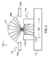
プラズマシース308を修正することにより、異なる角度に向けられた表面を有する3次元構造は、共形的又は等方的に処理される。図3を参照すると、本開示の一実施形態に従って3D構造を処理する技術が示されている。本実施形態においては、この技術は、3Dフォトレジストレリーフ形状114aに含まれるLER及びLWRを減らすために使用される。前述のように、LER及びLWRは、フォトレジストの硬化されていない部分が除去された後、光リソグラフィの間に3Dフォトレジストレリーフ形状114aに生じうる。本実施形態において、フォトレジストレリーフ形状114aに含まれるLER及びLWRは、フォトレジストレリーフ形状をイオン310に露光することによって減少しうる。
By modifying the plasma sheath 308, three-dimensional structures having surfaces oriented at different angles are processed conformally or isotropically. Referring to FIG. 3, a technique for processing a 3D structure according to one embodiment of the present disclosure is shown. In this embodiment, this technique is used to reduce LER and LWR contained in the 3D
図3に図示されるように、側面114a−1及び上面114a−2を有する3Dフォトレジストレリーフ形状114aは、基板112上に配置される。基板112及びフォトレジストレリーフ形状114aは、プラズマシース修正器312を含むプラズマ処理システム内に配置され、プラズマは、基板112の近傍に配置される。その後、プラズマ内のイオン310が、プラズマシース修正器部分312a及び312bの間の隙間を通って、フォトレジストレリーフ形状114aの表面に向けられる。図に示されるように、イオン310は様々な入射角度で入射する。
As illustrated in FIG. 3, a 3D
様々な実施形態において、イオン310は、フォトレジストレリーフ形状114aの側面114a−1及び上面114a−2に注入される。様々なイオン種が注入されうるが、いくつかの実施形態においては、ヘリウム(He)イオン又はアルゴン(Ar)イオンが注入される。フォトレジストのイオン露光時間は広範囲にわたるが、いくつかの実施形態において、露光時間全体は、約数十秒から数分まで多様である。
In various embodiments,
本発明に従って構成されたプラズマ処理システム(PSMシステム)のLWR/LER及びCDに関する効果を検証する実験を行った。以後、「PSMシステム」又は「PSMプラズマシステム」という用語はプラズマ処理システムを示し、このプラズマ処理システムは、プラズマの一部に隣接して配置される基板に向かうイオンの広範囲にわたる角度分布を提供するプラズマシース修正器を採用する。イオンの入射角とともに使用される「広い」「広範」又は「広範な角度範囲」という用語は、約5度以上の範囲に広がる一組の角を示す。プラズマシース修正器は、図2bに図示されるように、広範な角度範囲に分布されるイオン線量を含めた露光を提供するために使用される。プラズマシース修正器は、1以上の開口を有するプレートを有してもよく、それにより修正プラズマシースの形成が誘発され(要素308b参照)、イオンが広範な角度範囲にわたって基板上に衝突するようにプラズマからイオンを抽出することができる。いくつかの実施形態において、プラズマシース修正器の開口は、約0.1mmから10mmの幅を有してもよい。基板の広い範囲を露光するために、基板は、イオンに露光される基板の領域の大きさがスキャン長によって制御されるように、プラズマシース修正器の開口に対してスキャン可能であってもよい。
Experiments were conducted to verify the effects on LWR / LER and CD of a plasma processing system (PSM system) constructed according to the present invention. Hereinafter, the term “PSM system” or “PSM plasma system” refers to a plasma processing system that provides a wide angular distribution of ions toward a substrate disposed adjacent to a portion of the plasma. Adopt a plasma sheath corrector. The terms “wide”, “wide”, or “wide angular range” as used with ion incidence angles refer to a set of angles that extend over a range of about 5 degrees or more. The plasma sheath modifier is used to provide exposure including ion doses distributed over a wide angular range, as illustrated in FIG. 2b. The plasma sheath modifier may have a plate with one or more openings, thereby inducing the formation of a modified plasma sheath (see
再び図3を参照すると、一連の個々の実験において、約40nmの公称CDを有する一組の別々のフォトレジストラインは、一連の異なるプラズマ出力レベルのそれぞれにおける典型的な抽出プレートを使用して、4kVのArプラズマに露光された。フォトレジストラインが、出力300Wのプラズマに露光されたとき、約26%のLWRの減少が観察され、また、約20%のフォトレジストラインのCDの減少も観察された。フォトレジストラインが、代わって500Wのプラズマ出力レベルのプラズマに露光されたとき、CDの現象はほとんど観察されず、観察されたとしてもほんのわずかであった。しかしながら、LWRの減少は約11%であった。従って、より高いプラズマ出力を使用することは、好ましくないCDの減少を避けるためには効果的でありうるが、フォトレジストレリーフ形状を滑らかにするためにはそれほどの効果はないであろう。 Referring again to FIG. 3, in a series of individual experiments, a set of separate photoresist lines having a nominal CD of about 40 nm is used using a typical extraction plate at each of a series of different plasma power levels. Exposed to 4 kV Ar plasma. When the photoresist line was exposed to a 300 W power plasma, an LWR reduction of about 26% was observed and a CD reduction of about 20% of the photoresist line was also observed. When the photoresist line was exposed to a plasma with a plasma power level of 500 W instead, little or no CD phenomenon was observed. However, the LWR reduction was about 11%. Thus, using a higher plasma power may be effective to avoid undesired CD reduction, but will not be as effective to smooth the photoresist relief shape.
LWRの減少とCDの維持との間のこのトレードオフを克服するために、本開示の実施形態は、フォトレジストレリーフ形状が、第1のイオン線量率で1以上のイオン露光を受け、第1のイオン線量率よりも高い第2のイオン線量率で1以上の露光を受けるという新規な技術を採用する。いくつかの実施形態において、露光は、プラズマシース修正器312が、方向320にパターン化されたフォトレジストレリーフ形状114aを有する基板に対してスキャンされる、1以上のスキャンであってもよい。プラズマシース修正器312は、イオン310が抽出される開口322を有するプレートとすることができるので、プラズマシース修正器のいくつかの実施形態は、本明細書において、以下「抽出プレート」という。抽出プレートは、上述のようにプラズマシースの形状を修正する1以上の開口を有してもよい。多様な実施形態において、基板112は、抽出プレートの開口に対し方向320に沿ってスキャン可能である。従って、開口322の幅にかかわらず、多くのフォトレジストレリーフ形状114aを有する基板全体又は基板の所望の部分をスキャン中にイオン310に露光することができる。多様な実施形態において、プラズマ306は、連続プラズマ又はパルス化されたプラズマとすることができ、基板ホルダ304とプラズマ306との間のバイアスは、連続又はパルス信号とすることができる。
In order to overcome this trade-off between LWR reduction and CD maintenance, embodiments of the present disclosure provide that a photoresist relief shape undergoes one or more ion exposures at a first ion dose rate, and the first A new technique is adopted in which one or more exposures are performed at a second ion dose rate that is higher than the ion dose rate. In some embodiments, the exposure may be one or more scans in which the
いくつかの実施形態において、抽出プレートの一連のスキャンは、アルゴンプラズマ及び約750eVのイオンエネルギーを用いてパターン化されたフォトレジストレリーフ形状にわたって実施される。スキャンは、マルチセットポイントRFプラズマ(MSPRF)処理の一部として実行することができ、この処理において、プラズマのパワーセットポイントは変化しうる。そのため、第1の露光は、パターン化されたフォトレジストレリーフ形状にわたる抽出プレートのFR出力が第1のレベルに設定された1以上のスキャンであり、第2の露光は、RF出力が第1のレベルよりも高い第2のレベルに設定された抽出プレートの1以上のスキャンとすることができる。いくつかの実施形態において、1以上のスキャンを含む第1の露光は、比較的低いプラズマ出力で行われる。比較的低いプラズマ出力により、パターン化されたフォトレジストレリーフ形状に向かうイオンのイオン線量率が比較的低くなる。この比較的低いイオン線量率において、露光後、初期値からそれぞれの第2の値までのLWR/LER及びCDの両ラインにおいて、減少が観察される。続いて、比較的高いイオン線量率を生成する比較的高いプラズマ出力において、1以上のスキャンが行われる。第2の組のスキャンの後、第2の値から第3の値へのCDの増加が観察される。1組の例において、この多数のイオン線量率の処理を実行した後、LWR/LERの減少は、最大50%であり、一方、CDのばらつきは、第2の露光のイオン線量率に応じて、−2nmから+5nmの範囲であった。 In some embodiments, a series of scans of the extraction plate are performed over a patterned photoresist relief shape using an argon plasma and an ion energy of about 750 eV. The scan can be performed as part of a multi-setpoint RF plasma (MSPRF) process, in which the plasma power setpoint can change. Therefore, the first exposure is one or more scans where the FR output of the extraction plate over the patterned photoresist relief shape is set to the first level, and the second exposure has the RF output of the first There may be one or more scans of the extraction plate set to a second level higher than the level. In some embodiments, the first exposure including one or more scans is performed with a relatively low plasma power. The relatively low plasma power results in a relatively low ion dose rate of ions toward the patterned photoresist relief shape. At this relatively low ion dose rate, a decrease is observed in both the LWR / LER and CD lines from the initial value to the respective second value after exposure. Subsequently, one or more scans are performed at a relatively high plasma power that produces a relatively high ion dose rate. After the second set of scans, an increase in CD from the second value to the third value is observed. In one set of examples, after performing this multiple ion dose rate process, the LWR / LER decrease is up to 50%, while the CD variation depends on the ion dose rate of the second exposure. , -2 nm to +5 nm.
図4a−4d及び4e−4gは、フォトレジストレリーフ形状の典型的な処理の詳細を示す、パターン化されたフォトレジストレリーフ形状の側面断面図及び平面図である。この処理は、低いイオン線量率及び高いイオン線量率の露光を組み合わせている。図4a及び4eにおいて、初期の幅(CD)W1を有する1組のフォトレジストレリーフ形状402が、第1のイオン線量率で第1の角度範囲にわたってイオン404の露光を受ける。イオン404は、側壁406に衝突して、側壁の例えばLWR/LERといった粗さを減少させる。多様な実施形態において、イオン404は、例えばシステム300のようなシステムにより供給され、イオン線量率は、プラズマ出力、処理チャンバ内の圧力、処理チャンバ内のガス流を含むパラメータを調整することにより制御される。イオン線量率は、イオンエネルギーにも依存する。多様な実施形態に従って、イオン404に対する露光後、イオンに露光されたフォトレジストレリーフ形状408は、側壁410において図示されるように、より小さいCD(W2)と、より少ないラインラフネスとを示す。続く露出において、図4c及び4fに示されるように、イオン412は、第2の角度範囲(第1の角度範囲と類似しているか又は異なるものとすることができる)にわたって、イオン404に対する露光で使用された第1のイオン線量率よりも高い第2のイオン線量率で、フォトレジストレリーフ形状に向けられる。高いイオン線量率の第2の露光の後、その結果物であるフォトレジストレリーフ形状414は、フォトレジストレリーフ形状408のCDよりも大きなCD(W3)を示す。多様な実施形態において、イオン412への露光中のイオン線量率及び全イオン線量は、CDを所望の値に戻すように調整される。例えば、イオン線量率は、CDを元のCDであるW1に戻すように調整され、又は、CDを元のCDであるW1の予め定められた公差の範囲内に戻すように調整される。
4a-4d and 4e-4g are side cross-sectional and plan views of a patterned photoresist relief shape showing details of exemplary processing of the photoresist relief shape. This process combines a low ion dose rate and a high ion dose rate exposure. 4a and 4e, a set of
イオン412への露光の後、結果物としてのフォトレジストレリーフ形状414の側壁416は、イオン404及びイオン412への露光前の側壁406よりも平滑である。
After exposure to
前述のように、いくつかの実施形態において、より低い又はより高いイオン線量率の組合せは、初期CD及び最終CD、すなわち、それぞれW1及びW3の間の対応関係を提供するように設計される。従って、図4に示される複数のイオン露光処理の効果は、事実上CDを変更することなくフォトレジストの側壁を滑らかにすることにある。 As described above, in some embodiments, the combination of lower or higher ion dose rates is designed to provide a correspondence between the initial CD and final CD, ie, W1 and W3, respectively. Accordingly, the effect of the multiple ion exposure processes shown in FIG. 4 is to smooth the sidewalls of the photoresist without substantially changing the CD.
他の実施形態において、イオン412の線量率及び線量は、初期CDよりも大きい最終CDのW3を得るように設計される。例えば、リソグラフィ処理の後、対象となるフォトレジストレリーフ形状において計測されるCD(W1に対応する)は、その処理の公称CD又は目標CDよりも小さくてもよい。従って、ラインラフネスを改善するためにイオン404に露光した後、公称値に対するフォトレジストレリーフ形状のCDを回復させることが望ましい。そのため、イオン412への露光は、W1よりも大きくて目標CDを反映したW3に対応するCDを得るように設計される。
In other embodiments, the dose rate and dose of
さらに他の実施形態において、イオン404及び412への露光の順序を入れ替えて、高イオン線量率の露光を低イオン線量率の露光よりも先に実施してもよい。この方法では、初期フォトレジストレリーフ形状のCDであるW1は、第2のより低いイオン線量率の露光が行われる前に、値W4(図示なし)まで増加される。より低いイオン線量率の露光の後、ラインラフネスが減少され、CDがW4から、W1に近い又はW1と同一のW3まで減少される。しかしながら、フォトレジストレリーフ形状が密集している場合には、W1より大きいW4の隣接するフォトレジストレリーフ形状が、互いに群がり合ってその後の低イオン線量率露光の間に側壁の部分がイオン束を受けることを妨害するため、低イオン線量率の露光を最初に実施するのが好都合である。
In still other embodiments, the order of exposure to
多様な実施形態において、前述のように、イオン線量率は、パターン化されたフォトレジストレリーフ形状に多様な角度でイオンを照射するシステムのプラズマ出力を変化することにより制御される。再び図2aを参照すると、RFプラズマの場合、プラズマ出力は、RF発生器330からアンテナ332に送信される信号の振幅を変えることにより変化させることができる。プラズマ出力レベルをより高くすると、プラズマのイオン密度はより高くなり、プラズマ306からより高いイオン線量率でイオンを抽出することができる。
In various embodiments, as described above, the ion dose rate is controlled by changing the plasma output of a system that irradiates ions at various angles into a patterned photoresist relief shape. Referring again to FIG. 2a, in the case of RF plasma, the plasma output can be varied by changing the amplitude of the signal transmitted from the RF generator 330 to the
図5aは、プラズマ出力曲線502の例を示しており、プラズマ出力が、曲線の第1の期間504にわたるレベルP1とプラズマ出力曲線502の第2の期間506にわたるレベルP2との間で変化している。多様な実施形態では、レベルP1は、最初に基板に適用される、より低いイオン線量率に対応させ、レベルP2は、より低いイオン線量率の後に適用される、より高いイオン線量率に対応させることができる。図3も参照すると、第1出力レベルP1は、イオンをフォトレジストレリーフ形状114aに向ける抽出プレート(例えば、プラズマシース修正器312)について、基板112の方向320に、3つの連続した経路(スキャン1−スキャン3)の期間に適用される。第2出力レベルP2は、その後の一連のスキャン(スキャン4及び5)の間に適用される。スキャンの全数及び全期間が、プラズマ出力レベルP1及びP2と同様に、所望の平滑化及びフォトレジストレリーフ形状114aの最終CDを生成するように調節されることが理解されるであろう。上述のように、プラズマ出力は、基板をイオンに露光している間連続して又はパルスで適用されてもよい。
FIG. 5 a shows an example of a
図5bは、一連の高イオン線量率のスキャンが一連の低イオン線量率のスキャンと交互に行われる他の一実施形態を示す。このことは、本実施形態において、連続するスキャン(スキャン1−スキャン6)の間にP1とP2とのプラズマ出力レベルを交互に行うことにより達成される。各スキャンは、抽出プレートに関する基板の単一のスキャンに対応させることができる。曲線512は、プラズマ出力がP1に維持される期間514と、プラズマ出力がP2に維持される期間516とを交互に行うプラズマ出力曲線を示す。図示されるように、1つのスキャン期間に、単一の出力レベルが適用される。スキャン1の後、CDが徐々に減少するのと同時に、フォトレジストレリーフ形状の側壁のラフネスが徐々に改善される。スキャン2の後、スキャン1によって生成されたCDの漸次的な減少が、部分的に又は全体的に回復される(又は、スキャン1の前の初期値を上回って増加される)。スキャン1と2との間の露光処理が、それに続くスキャンにおいても繰り返され、比較的高いイオン線量率によりCDが徐々に回復される一連のステップとを交互に繰り返すことにより、フォトレジストレリーフ形状のラインラフネスを一連のステップ(奇数番号のスキャンに対応)において減少する。
FIG. 5b shows another embodiment in which a series of high ion dose rate scans are alternated with a series of low ion dose rate scans. In the present embodiment, this is achieved by alternately performing plasma output levels of P1 and P2 between successive scans (scan 1 to scan 6). Each scan can correspond to a single scan of the substrate for the extraction plate. A
図5bも、プラズマ出力曲線512に従って、レジストラインの処理の間の様々な時点におけるフォトレジスト測定の例を示す。露光前の初期ラインラフネス及びCD測定は、それぞれLWR1及びCD1によって示されている。出力レベルP1及びP2の各1回のスキャンを含む第1の露光サイクルの後、LWRは、値LWR2まで減少できる。CDはその前の露光と同様であり、すなわちCD1である。第2のサイクルの後、LWRは、値LWR3まで減少でき、CDは、ここでもCD1に維持できる。第3のサイクルの後、LWRは、値LWR4まで減少し、CDは、ここでもCD1に維持される。従って、フォトレジストレリーフ形状を処理するためのプラズマシース修正器と合わせてプラズマ出力曲線512を適用することによる効果は、CDに影響を与えることなくラフネスをLWR1からLWR4に減少させることにある。例えばラインラフネスの減少のようなフォトレジストの側壁の平滑化も、スキャン2、スキャン4及びスキャン6のスキャンの間に起こっていることに留意すべきである。
FIG. 5b also shows an example of photoresist measurements at various times during the processing of the resist line according to the
連続プラズマのプラズマ出力の変化の他、イオン線量率は、出力をパルス状のプラズマに適用することにより制御される。高プラズマ出力セットポイントは、各プラズマパルスに設定され、例えば1秒を構成する10パルスごと等のプラズマパルスの一期間において、より低いイオン線量率である第1イオン線量率を生成する。このような場合、イオン線量率は平均イオン線量率により特徴付けられ、その詳細は後述する。 In addition to the change in plasma output of the continuous plasma, the ion dose rate is controlled by applying the output to a pulsed plasma. The high plasma power setpoint is set for each plasma pulse and generates a first ion dose rate, which is a lower ion dose rate, during one period of the plasma pulse, eg, every 10 pulses that make up 1 second. In such a case, the ion dose rate is characterized by an average ion dose rate, the details of which will be described later.
パルス化されたプラズマの使用により、後述するように、最終的なフォトレジストレリーフ形状のラインラフネス及びCDの他の制御が可能になる。例えば、プラズマパルスにより、ベースライン処理のプラズマパルスの生成を調整することにより、必要に応じたイオン線量率を柔軟に修正することができる。一例において、パルス化されたプラズマの全パルスに適用される300WのRFプラズマ出力セットポイントを使用するベースライン処理の生成により、目標のラインラフネスを減少させることができる。パルス化されたプラズマの全パルスに適用される500WのRFプラズマ出力セットポイントを採用する方法によれば、CDを約10nm増加できることが観察される。従って、第1の組の基板に対して、300Wのプラズマ出力及び500Wのプラズマ出力の組合せ処理方法により、フォトレジストレリーフ形状の所望のラインラフネス及びCDを生成できる。 The use of pulsed plasma allows the final photoresist relief shape line roughness and other control of the CD, as described below. For example, by adjusting the generation of the plasma pulse for the baseline processing by the plasma pulse, the ion dose rate can be flexibly corrected as necessary. In one example, the target line roughness can be reduced by generating a baseline process using a 300 W RF plasma power setpoint applied to all pulses of the pulsed plasma. It is observed that the CD can be increased by about 10 nm according to the method employing a 500 W RF plasma power setpoint applied to all pulses of the pulsed plasma. Therefore, the desired line roughness and CD of the photoresist relief shape can be generated on the first set of substrates by the combined processing method of the plasma output of 300 W and the plasma output of 500 W.
しかしながら、他の組の基板に対して、300W及び500WのRFプラズマ出力の露光を実行した後のフォトレジストレリーフ形状の最終的なCDは5nm大きく決定されうる。従って、フォトレジストの膨張を減少させるために、より高いイオン線量率(500W)の処理に変更することが望ましい。この場合、第2の露光において、高プラズマ出力セットポイント(500W)が、1つおきのパルスに適用され、より低いプラズマ出力セットポイント(例えば300W)が、1つおきのパルスに適用される。これにより、ベースラインの300Wのプラズマ出力生成と不変の500Wのプラズマ出力生成との中間のイオン線量率が生成される。この中間イオン線量率は、第2の組の基板に対してCDの所望の増加を生じる結果となる。 However, the final CD of the photoresist relief shape after performing exposure with 300 W and 500 W RF plasma power for other sets of substrates can be determined to be 5 nm larger. Therefore, it is desirable to change to a higher ion dose rate (500 W) process to reduce photoresist expansion. In this case, in the second exposure, a high plasma power setpoint (500 W) is applied to every other pulse, and a lower plasma power setpoint (eg, 300 W) is applied to every other pulse. This produces an intermediate ion dose rate between the baseline 300 W plasma power generation and the unchanged 500 W plasma power generation. This intermediate ion dose rate results in the desired increase in CD for the second set of substrates.
図6a−6cは、平均イオン線量率が比較的低い値と高い値との間で変化するパルス化されたプラズマ処理の代替実施形態を示す。図6aにおいて、曲線602は、一連の低出力パルス608が第1の期間604の間に適用され、それに続いて一連の高出力パルス610が第2の期間606の間に適用されるプラズマ出力曲線を示す。プラズマがかかっているときの出力レベルは、低出力パルス608においてP3であり、高出力パルス610においてP4である。
Figures 6a-6c show an alternative embodiment of pulsed plasma treatment where the average ion dose rate varies between a relatively low value and a high value. In FIG. 6 a,
いくつかの実施形態において、パルス608及び610は、100マイクロ秒から最大数ミリ秒の桁数のパルス持続時間に対して適用される。多様な実施形態において、例えば図5に示されるように、期間604及び/又は606は、数ミリ秒から最大数秒まで拡張することができ、1以上のスキャンの期間に相当する。従って、単一期間604又は606の間、多くのパルスが適用され、例えば、数十、数百又は数千のパルスが適用される。そのため、単一期間604又は606の間のイオン線量率は、その期間の継続時間中の平均イオン線量率により特徴付けられる。特に、イオン線量率は、曲線640により示され、曲線640において、イオン線量率は、プラズマの「オン」及び「オフ」の期間を構成する時間の経過とともに、平均化されている。例えば、イオン線量率は、パルスのオン及びオフの期間の合計と等しいパルス期間にわたって平均化される。従って、曲線640は、1以上のパルス期間にわたる時間平均イオン線量率(束)を示している。
In some embodiments,
図6b及び6cに示されるように、同一の平均イオン線量曲線640が異なるパルスの組合せから生じる。図6bにおいて、プラズマ出力曲線612の第1の期間604は、図6aの期間604により表現される低イオン線量率露光に対応し、出力が、一連の低出力パルス608におけるレベルP3で適用される。第2の期間616は、1つおきのパルス620における、P4よりも高いプラズマ出力P5を供給することにより生じる高イオン線量率の露光に対応する。パルス620には、出力レベルP3に対応する低出力パルス618が分散されている。出力レベルP3とP5との交互のパルスの組合せにより、図6aの平均イオン線量率と同じ平均イオン線量率640bが得られる。図6cにおいて、プラズマ出力曲線622の第1の期間604は、図6aと同様であり、出力が、一連の低出力パルス608におけるレベルP3で適用される。第2の期間626は、3つおきのパルス630における、P4及びP5よりも高い出力P6を供給することにより生じ、他の3つの低出力パルス628は出力レベルP3で供給される。出力レベルP6における3つおきのパルスと、P3の他の3つのパルスとを供給するという組合せにより、図6a及び6bの平均線量率と同一の平均線量率640bが得られる。
As shown in FIGS. 6b and 6c, the same average
いくつかの実施形態において、比較的低いイオン線量率の処理は、より高い後部の基板の冷却器と組み合わせられ、比較的高いイオン線量率の処理は、比較的低い後部の冷却器と組み合わせられる。いくつかの実施形態において、基板後部冷却器及びそれによる基板の温度は、冷却管336内の液体の種類又は液体の流率を制御することにより変化させうる。しかしながら、後部冷却器の制御は、他の機器、例えば既知のペルチェ冷却器(図示なし)によって提供される。提供される後部冷却部をより少なくし、それによって、より高い線量率の露光の間により高い基板温度を生成することにより、より高い温度においてより大きなCDの膨張が生じるため、CDの膨張は拡大される。
In some embodiments, a relatively low ion dose rate process is combined with a higher back substrate cooler and a relatively high ion dose rate process is combined with a relatively low back cooler. In some embodiments, the temperature of the substrate back cooler and thereby the substrate can be varied by controlling the type of liquid or the liquid flow rate in the
前述のように、いくつかの実施形態において、より低いイオン線量率の露光におけるイオンの第1の角度範囲は、より高いイオン線量率のイオンの第2の角度範囲と異なりうる。
As described above, in some embodiments, the first angular range of ions in a lower ion dose rate exposure may be different than the second angular range of higher ion dose rate ions .
本明細書に記載された方法は、例えば、命令を実行することができる機械により読み取ることが可能なコンピュータ可読記憶媒体に、命令のプログラムを具体化することにより自動化できることが明らかである。汎用コンピュータは、そのような機械の一例である。この技術分野において周知の適切な記憶媒体の限定されない典型的なリストは、例えば、読取可能又は書込可能CD、フラッシュメモリチップ(例えばサムドライブ)、多様な磁気記憶媒体等のような装置を含む。 It will be apparent that the methods described herein can be automated by, for example, embodying a program of instructions on a computer readable storage medium readable by a machine capable of executing the instructions. A general purpose computer is an example of such a machine. A non-limiting exemplary list of suitable storage media known in the art includes devices such as, for example, readable or writable CDs, flash memory chips (eg, thumb drives), various magnetic storage media, and the like. .
要約すると、本発明は、例えばフォトレジストレリーフ形状等のパターン化された形状のラインラフネスを減少させる一方、その結果生じる形状のCDを独立して制御するという、新規性及び進歩性を有する方法及びシステムを提供する。 In summary, the present invention is a novel and inventive method that reduces the line roughness of a patterned shape, such as a photoresist relief shape, while independently controlling the resulting CD of the shape and Provide a system.
本発明は、本明細書に記載された具体的な実施形態により範囲が制限されるものではない。実際、本明細書の記載に加えて、他の多様な実施形態及び本開示に対する変更が、前述の記載及び添付図面から、本技術分野の通常の知識を有する者に対して明確であろう。例えば、上述の詳細な実施形態においては、フォトレジスト処理について記載されていたが、他の実施形態は、例えば、電子ビームレジスト、X線レジスト又はナノインプリントリソグラフィレジスト等のレジストの処理を含む。 The present invention is not to be limited in scope by the specific embodiments described herein. Indeed, in addition to the description herein, various other embodiments and modifications to the present disclosure will become apparent to those with ordinary skill in the art from the foregoing description and accompanying drawings. For example, in the detailed embodiments described above, photoresist processing has been described, but other embodiments include processing of resists such as, for example, electron beam resists, x-ray resists or nanoimprint lithography resists.
従って、このような他の実施形態及び変更は、本開示の範囲に含まれることが意図される。さらに、本開示は、本明細書において、特定の実施形態で、特定の環境下で、特定の目的のために記載されているが、本技術分野における通常の知識を有する者は、その実用性がこれらに限定されず、本開示が如何なる環境下で如何なる目的においても有益に実施できることを理解できるであろう。従って、本開示の主題は、本明細書に記載された本開示の全ての範囲及び精神を考慮して解釈されるべきである。
Accordingly, such other embodiments and modifications are intended to be included within the scope of this disclosure. Further, while the present disclosure has been described herein for specific purposes, in specific embodiments and in specific environments, those having ordinary skill in the art may find its utility. It will be understood that the present disclosure is not limited to these and can be beneficially implemented for any purpose in any environment. Accordingly, the subject matter of the present disclosure should be construed in view of the full scope and spirit of the present disclosure as described herein.
Claims (16)
第1の露光において、前記初期ラインラフネスを第2ラインラフネスに減少させるように構成された第1の角度範囲及び第1のイオン線量率で、前記フォトレジストレリーフ形状にイオンを向けるステップと、
第2の露光において、前記第1のイオン線量率よりも高い第2のイオン線量率であって、前記フォトレジストレリーフ形状を膨張させるように構成され、前記第2ラインラフネスよりも小さい第3ラインラフネスに前記フォトレジストレリーフ形状を平滑化する、第2のイオン線量率で、前記フォトレジストレリーフ形状にイオンを向けるステップと、
を含む処理方法。 A method for processing a photoresist relief shape on a substrate having an initial line roughness and an initial critical dimension, comprising:
Directing ions in the photoresist relief shape at a first angle range and a first ion dose rate configured to reduce the initial line roughness to a second line roughness in a first exposure;
In the second exposure, the first and a second ion dose rate greater than the ion dose rate, the photoresist is configured to relief shape inflated, third smaller than the previous SL second line roughness Smoothing the photoresist relief shape to line roughness, directing ions to the photoresist relief shape at a second ion dose rate; and
Processing method.
前記第2の露光の間に、前記基板を前記第1の温度よりも高い第2の温度に冷却するステップと、
をさらに含む、請求項1に記載の方法。 Cooling the substrate having the photoresist relief shape to a first temperature during the first exposure;
Cooling the substrate to a second temperature higher than the first temperature during the second exposure;
The method of claim 1, further comprising:
プラズマシース及びイオンを有するプラズマを生成するステップと、
前記プラズマ及び前記プラズマシースの間に規定される境界の形状を修正するように機能する開口を規定する抽出プレートを提供するステップと、
前記フォトレジストレリーフ形状を有する基板と、前記修正された形状を有する前記境界を越えて前記フォトレジストレリーフ形状にイオンを引き込むように構成された前記プラズマとの間に、バイアスを供給するステップと、
をさらに含む、請求項1に記載の方法。 Directing ions by the first and second exposures,
Generating a plasma having a plasma sheath and ions;
Providing an extraction plate defining an opening that functions to modify a shape of a boundary defined between the plasma and the plasma sheath;
Providing a bias between the substrate having the photoresist relief shape and the plasma configured to draw ions into the photoresist relief shape across the boundary having the modified shape;
The method of claim 1, further comprising:
より高い第2のプラズマ出力レベルで前記第2の露光を実行するステップと、
を含む、請求項8に記載の方法。 Performing the first exposure at a first plasma power level;
Performing the second exposure at a higher second plasma power level;
The method of claim 8 comprising:
前記第2の露光の間に、前記基板に対して、前記抽出プレートの1以上のスキャンを実行するステップと、
を含む、請求項8に記載の方法。 Performing one or more scans of the extraction plate configured to supply ions over an angular range to the substrate having the photoresist relief shape during the first exposure;
Performing one or more scans of the extraction plate on the substrate during the second exposure;
The method of claim 8 comprising:
前記第2の露光の間に、前記第2の露光の期間にわたる平均プラズマ出力が第1の露光の期間にわたる平均プラズマ出力よりも高い第2の出力レベルで、前記プラズマの第2の一連のパルスを供給するステップと、
を含む、請求項8に記載の方法。 Providing a first series of pulses of plasma at a first power level during the first exposure;
During the second exposure, a second series of pulses of the plasma at a second power level where the average plasma power over the second exposure period is higher than the average plasma power over the first exposure period. Supplying a step;
The method of claim 8 comprising:
プラズマシースを有するプラズマを生成するように構成されたプラズマ源と、
前記プラズマと前記基板との間に配置され、ある角度範囲にわたってイオンを前記基板に向けるように構成された抽出プレートと、
前記プラズマに対する前記基板の露光条件を変化させるように機能する調整器であって、第1の露光の間に、第1のイオン線量率及び第1の角度広がりでイオンが前記フォトレジストレリーフ形状に向けられ、第2の露光の間に、前記第1のイオン線量率よりも高い第2のイオン線量率でイオンが前記フォトレジストレリーフ形状に向けられ、前記第1の露光は、前記初期ラインラフネスを第2ラインラフネスに減少させるように構成され、前記第2の露光は、前記フォトレジストレリーフ形状を膨張させて平滑化するように構成され、前記第1及び第2の露光の後、前記フォトレジストレリーフ形状の第3ラインラフネスが第2ラインラフネスよりも小さく、第3のクリティカルディメンションが前記第2のクリティカルディメンションよりも大きくなるように機能する調整器と、
を有する処理システム。 A photoresist relief processing system on a substrate,
A plasma source configured to generate a plasma having a plasma sheath;
An extraction plate disposed between the plasma and the substrate and configured to direct ions toward the substrate over a range of angles;
An adjuster that functions to change the exposure conditions of the substrate to the plasma, wherein during the first exposure, ions are transformed into the photoresist relief shape with a first ion dose rate and a first angular spread. Directed and during a second exposure, ions are directed to the photoresist relief shape at a second ion dose rate that is higher than the first ion dose rate, and the first exposure comprises the initial line roughness. Is reduced to a second line roughness, and the second exposure is configured to expand and smooth the photoresist relief shape, and after the first and second exposures, the third line roughness small fence than the second line roughness of resist relief shape, the third critical dimension is the second critical dimension A regulator that functions to be increased,
Having a processing system.
第1の露光において、前記フォトレジストレリーフ形状は前記初期クリティカルディメンションより小さい第2のクリティカルディメンションを示し、前記フォトレジストレリーフ形状が前記初期ラインラフネスより小さい第2ラインラフネスを示すまで、第1の線量率及び第1の角度広がりで、イオンを前記フォトレジストレリーフ形状に向けるステップと、
第2の露光において、前記フォトレジストレリーフ形状が前記第2のクリティカルディメンションより大きい第3のクリティカルディメンションに膨張して前記第2ラインラフネスより小さい第3ラインラフネスに平滑化するまで、前記第1の線量率よりも大きい第2の線量率で、イオンを前記フォトレジストレリーフ形状に向けるステップと、
を含む処理方法。
A method for processing a photoresist relief shape on a substrate having an initial line edge roughness and an initial critical dimension comprising:
In a first exposure, the photoresist relief shape exhibits a second critical dimension that is less than the initial critical dimension, and a first dose until the photoresist relief shape exhibits a second line roughness that is less than the initial line roughness. Directing ions into the photoresist relief shape at a rate and a first angular spread;
In the second exposure, up to the photoresist relief profile is smoothed before Symbol second line roughness is less than the third line roughness expands the second critical dimension larger than the third critical dimension, the first Directing ions into the photoresist relief shape at a second dose rate greater than the dose rate of
Processing method.
Applications Claiming Priority (3)
| Application Number | Priority Date | Filing Date | Title |
|---|---|---|---|
| US13/099,432 | 2011-05-03 | ||
| US13/099,432 US8354655B2 (en) | 2011-05-03 | 2011-05-03 | Method and system for controlling critical dimension and roughness in resist features |
| PCT/US2012/035218 WO2012151108A1 (en) | 2011-05-03 | 2012-04-26 | Method and system for controlling critical dimension and roughness in resist features |
Publications (3)
| Publication Number | Publication Date |
|---|---|
| JP2014515889A JP2014515889A (en) | 2014-07-03 |
| JP2014515889A5 JP2014515889A5 (en) | 2015-04-02 |
| JP6091490B2 true JP6091490B2 (en) | 2017-03-08 |
Family
ID=46125505
Family Applications (1)
| Application Number | Title | Priority Date | Filing Date |
|---|---|---|---|
| JP2014509322A Active JP6091490B2 (en) | 2011-05-03 | 2012-04-26 | Method and system for controlling critical dimension and roughness in resist shape |
Country Status (6)
| Country | Link |
|---|---|
| US (2) | US8354655B2 (en) |
| JP (1) | JP6091490B2 (en) |
| KR (1) | KR101911330B1 (en) |
| CN (1) | CN103620730B (en) |
| TW (1) | TWI532071B (en) |
| WO (1) | WO2012151108A1 (en) |
Families Citing this family (15)
| Publication number | Priority date | Publication date | Assignee | Title |
|---|---|---|---|---|
| US8354655B2 (en) * | 2011-05-03 | 2013-01-15 | Varian Semiconductor Equipment Associates, Inc. | Method and system for controlling critical dimension and roughness in resist features |
| US8974683B2 (en) * | 2011-09-09 | 2015-03-10 | Varian Semiconductor Equipment Associates, Inc. | Method and system for modifying resist openings using multiple angled ions |
| CN104345568A (en) * | 2013-08-07 | 2015-02-11 | 中芯国际集成电路制造(上海)有限公司 | Method for reducing photoresist figure linewidth roughness |
| CN104465333B (en) * | 2013-09-17 | 2017-12-29 | 中芯国际集成电路制造(上海)有限公司 | The forming method of photoetching offset plate figure, the forming method of transistor gate |
| US9520267B2 (en) * | 2014-06-20 | 2016-12-13 | Applied Mateirals, Inc. | Bias voltage frequency controlled angular ion distribution in plasma processing |
| US9837254B2 (en) | 2014-08-12 | 2017-12-05 | Lam Research Corporation | Differentially pumped reactive gas injector |
| US10825652B2 (en) | 2014-08-29 | 2020-11-03 | Lam Research Corporation | Ion beam etch without need for wafer tilt or rotation |
| US9406535B2 (en) | 2014-08-29 | 2016-08-02 | Lam Research Corporation | Ion injector and lens system for ion beam milling |
| US9536748B2 (en) | 2014-10-21 | 2017-01-03 | Lam Research Corporation | Use of ion beam etching to generate gate-all-around structure |
| US10935889B2 (en) | 2015-05-13 | 2021-03-02 | Tokyo Electron Limited | Extreme ultra-violet sensitivity reduction using shrink and growth method |
| US9779955B2 (en) | 2016-02-25 | 2017-10-03 | Lam Research Corporation | Ion beam etching utilizing cryogenic wafer temperatures |
| DE102016119437A1 (en) * | 2016-10-12 | 2018-04-12 | scia Systems GmbH | Method for processing a surface by means of a particle beam |
| DE102016119791A1 (en) * | 2016-10-18 | 2018-04-19 | scia Systems GmbH | Method and device for processing a surface of a substrate by means of a particle beam |
| KR20180082851A (en) * | 2017-01-11 | 2018-07-19 | 삼성전자주식회사 | Method for forming patterns in a semiconductor device and method for manufacturing a semiconductor device using the same |
| US11495436B2 (en) * | 2020-04-30 | 2022-11-08 | Tokyo Electron Limited | Systems and methods to control critical dimension (CD) shrink ratio through radio frequency (RF) pulsing |
Family Cites Families (10)
| Publication number | Priority date | Publication date | Assignee | Title |
|---|---|---|---|---|
| FR2716547A1 (en) * | 1994-02-24 | 1995-08-25 | Fujitsu Ltd | Method for forming a resist pattern and for manufacturing a semiconductor device. |
| US7838850B2 (en) * | 1999-12-13 | 2010-11-23 | Semequip, Inc. | External cathode ion source |
| EP1630849B1 (en) * | 2004-08-27 | 2011-11-02 | Fei Company | Localized plasma processing |
| CN101563759B (en) * | 2006-10-30 | 2011-08-03 | 日本航空电子工业株式会社 | Method of working solid surface with gas cluster ion beam |
| JP5108489B2 (en) | 2007-01-16 | 2012-12-26 | 株式会社日立ハイテクノロジーズ | Plasma processing method |
| US8623171B2 (en) | 2009-04-03 | 2014-01-07 | Varian Semiconductor Equipment Associates, Inc. | Plasma processing apparatus |
| US7767977B1 (en) * | 2009-04-03 | 2010-08-03 | Varian Semiconductor Equipment Associates, Inc. | Ion source |
| US8778603B2 (en) * | 2010-03-15 | 2014-07-15 | Varian Semiconductor Equipment Associates, Inc. | Method and system for modifying substrate relief features using ion implantation |
| US8435727B2 (en) | 2010-10-01 | 2013-05-07 | Varian Semiconductor Equipment Associates, Inc. | Method and system for modifying photoresist using electromagnetic radiation and ion implantation |
| US8354655B2 (en) * | 2011-05-03 | 2013-01-15 | Varian Semiconductor Equipment Associates, Inc. | Method and system for controlling critical dimension and roughness in resist features |
-
2011
- 2011-05-03 US US13/099,432 patent/US8354655B2/en active Active
-
2012
- 2012-04-25 TW TW101114778A patent/TWI532071B/en active
- 2012-04-26 WO PCT/US2012/035218 patent/WO2012151108A1/en active Application Filing
- 2012-04-26 JP JP2014509322A patent/JP6091490B2/en active Active
- 2012-04-26 KR KR1020137031655A patent/KR101911330B1/en active IP Right Grant
- 2012-04-26 CN CN201280027207.7A patent/CN103620730B/en active Active
-
2013
- 2013-01-14 US US13/740,663 patent/US8698109B2/en active Active
Also Published As
| Publication number | Publication date |
|---|---|
| JP2014515889A (en) | 2014-07-03 |
| US20120280140A1 (en) | 2012-11-08 |
| KR101911330B1 (en) | 2018-12-19 |
| US8698109B2 (en) | 2014-04-15 |
| TW201250410A (en) | 2012-12-16 |
| KR20140025497A (en) | 2014-03-04 |
| WO2012151108A1 (en) | 2012-11-08 |
| US8354655B2 (en) | 2013-01-15 |
| CN103620730B (en) | 2016-02-24 |
| US20130135598A1 (en) | 2013-05-30 |
| CN103620730A (en) | 2014-03-05 |
| TWI532071B (en) | 2016-05-01 |
Similar Documents
| Publication | Publication Date | Title |
|---|---|---|
| JP6091490B2 (en) | Method and system for controlling critical dimension and roughness in resist shape | |
| JP5728566B2 (en) | Method and system for altering patterned features of a substrate using ion implantation | |
| JP5858496B2 (en) | Method and system for modifying patterned photoresist using multi-step ion implantation | |
| TWI539495B (en) | Method of treating workpiece and plasma processing | |
| JP5773319B2 (en) | Method for reducing the surface roughness of resist features and method for correcting the roughness of patterning resist features | |
| JP2013527595A5 (en) | ||
| WO2012138707A1 (en) | Method and system for post-etch treatment of patterned substrate features | |
| JP2014515889A5 (en) | ||
| US8974683B2 (en) | Method and system for modifying resist openings using multiple angled ions | |
| KR20130124149A (en) | Method and system for modifying substrate patterned features using ion implantion | |
| JP2018508815A (en) | Multiple exposure processing for processing patterning features | |
| JP6270882B2 (en) | Large mesh partial batch exposure method electron beam lithography method | |
| RU2700231C1 (en) | Method of forming three-dimensional structures of functional layer topological elements on the surface of substrates | |
| Cornago et al. | Large area periodic nanostructures: influence of several process parameters | |
| Ma et al. | Analysis of the resolution doubling technique of high-resolution gratings by x-ray lithography |
Legal Events
| Date | Code | Title | Description |
|---|---|---|---|
| A521 | Request for written amendment filed |
Free format text: JAPANESE INTERMEDIATE CODE: A523 Effective date: 20150209 |
|
| A621 | Written request for application examination |
Free format text: JAPANESE INTERMEDIATE CODE: A621 Effective date: 20150209 |
|
| A131 | Notification of reasons for refusal |
Free format text: JAPANESE INTERMEDIATE CODE: A131 Effective date: 20151208 |
|
| A521 | Request for written amendment filed |
Free format text: JAPANESE INTERMEDIATE CODE: A523 Effective date: 20160304 |
|
| A131 | Notification of reasons for refusal |
Free format text: JAPANESE INTERMEDIATE CODE: A131 Effective date: 20160802 |
|
| A521 | Request for written amendment filed |
Free format text: JAPANESE INTERMEDIATE CODE: A523 Effective date: 20161020 |
|
| TRDD | Decision of grant or rejection written | ||
| A01 | Written decision to grant a patent or to grant a registration (utility model) |
Free format text: JAPANESE INTERMEDIATE CODE: A01 Effective date: 20170110 |
|
| A61 | First payment of annual fees (during grant procedure) |
Free format text: JAPANESE INTERMEDIATE CODE: A61 Effective date: 20170207 |
|
| R150 | Certificate of patent or registration of utility model |
Ref document number: 6091490 Country of ref document: JP Free format text: JAPANESE INTERMEDIATE CODE: R150 |
|
| R250 | Receipt of annual fees |
Free format text: JAPANESE INTERMEDIATE CODE: R250 |
|
| R250 | Receipt of annual fees |
Free format text: JAPANESE INTERMEDIATE CODE: R250 |
|
| R250 | Receipt of annual fees |
Free format text: JAPANESE INTERMEDIATE CODE: R250 |
|
| R250 | Receipt of annual fees |
Free format text: JAPANESE INTERMEDIATE CODE: R250 |
|
| R250 | Receipt of annual fees |
Free format text: JAPANESE INTERMEDIATE CODE: R250 |