JP6091216B2 - Image signal processing apparatus, control method therefor, and imaging apparatus - Google Patents
Image signal processing apparatus, control method therefor, and imaging apparatus Download PDFInfo
- Publication number
- JP6091216B2 JP6091216B2 JP2013000943A JP2013000943A JP6091216B2 JP 6091216 B2 JP6091216 B2 JP 6091216B2 JP 2013000943 A JP2013000943 A JP 2013000943A JP 2013000943 A JP2013000943 A JP 2013000943A JP 6091216 B2 JP6091216 B2 JP 6091216B2
- Authority
- JP
- Japan
- Prior art keywords
- signal processing
- image signal
- image
- signal
- processing
- Prior art date
- Legal status (The legal status is an assumption and is not a legal conclusion. Google has not performed a legal analysis and makes no representation as to the accuracy of the status listed.)
- Expired - Fee Related
Links
Images


Description
本発明は、入力画像信号を処理して表示装置に表示する場合の表示遅延時間を短縮する技術に関する。 The present invention relates to a technique for reducing a display delay time when an input image signal is processed and displayed on a display device.
デジタルビデオカメラやデジタルカメラ等の撮像装置は、被写体像の確認用に表示装置を備え、液晶や有機EL(エレクトロルミネッセンス)のディスプレイ(パネル)や電子ビューファインダー(EVF)等が使用される。表示画面にはユーザが撮影する被写体像、つまり記録している画像を所定の画質でリアルタイムに表示することができる。近年、記録画像の多画素化や、画質改善処理の多機能化に伴い、信号処理に時間がかかると表示遅延が生じる。表示遅延により、パンニングやチルティング、ズーミング等のカメラ操作時にユーザに違和感を与え、構図やフォーカス状態等の確認が難しくなる場合がある。表示遅延量は撮影フレーム周波数に依存し、フレーム周波数が低い場合に表示遅延量が大きくなる。撮像装置の構成にもよるが、例えば、フレーム周波数24Hz(ヘルツ)の場合は、60Hzの場合よりも表示遅延量が2.5倍大きくなる。 An imaging device such as a digital video camera or a digital camera includes a display device for confirming a subject image, and a liquid crystal display, an organic EL (electroluminescence) display (panel), an electronic viewfinder (EVF), or the like is used. On the display screen, a subject image photographed by the user, that is, a recorded image can be displayed in real time with a predetermined image quality. In recent years, with the increase in the number of pixels of a recorded image and the increase in functionality of image quality improvement processing, display delay occurs when signal processing takes time. Due to the display delay, the user may feel uncomfortable when operating the camera such as panning, tilting, and zooming, and it may be difficult to check the composition, focus state, and the like. The display delay amount depends on the shooting frame frequency, and the display delay amount increases when the frame frequency is low. Although depending on the configuration of the imaging device, for example, when the frame frequency is 24 Hz (Hertz), the display delay amount is 2.5 times larger than when the frame frequency is 60 Hz.
テレビジョン装置においても画質改善処理の多機能化により同様の問題がある。テレビジョン装置にゲーム機器を接続してユーザがゲーム操作を行う場合、テレビジョン装置で画質改善処理を行うと数フレーム時間の表示遅延が生じる。ユーザ操作の遅れが原因でゲーム結果が変わる場合や、ユーザに違和感を与える場合があった。そこで、表示遅延量の低減のために、画質改善処理を簡略化した低遅延用の処理を行う方法や、フレームメモリの記憶処理と読み出し処理を同時に行う制御方法が特許文献1に開示されている。 A television apparatus has the same problem due to the multi-functionality of image quality improvement processing. When a game device is connected to a television apparatus and a user performs a game operation, a display delay of several frame times occurs when image quality improvement processing is performed on the television apparatus. In some cases, the game result may change due to a delay in user operation, or the user may feel uncomfortable. Therefore, in order to reduce the display delay amount, Patent Document 1 discloses a method for performing low-delay processing that simplifies image quality improvement processing, and a control method for performing frame memory storage processing and readout processing simultaneously. .
従来の装置では、入力画像信号を処理しつつ、表示用の画像信号を生成して表示部に出力するまでの表示遅延時間を如何にして短縮するかが課題である。従来の技術では撮像装置等への適用において、撮影中の画像を表示装置に表示する場合の表示遅延時間を短縮することが困難である。
本発明は、入力画像信号を処理しつつ、表示用の画像信号を生成して表示部に出力するまでの表示遅延時間を短縮することを目的とする。
A problem with conventional devices is how to reduce the display delay time from the generation of an image signal for display to output to the display unit while processing the input image signal. In the conventional technique, it is difficult to shorten the display delay time when displaying an image being shot on a display device when applied to an imaging device or the like.
It is an object of the present invention to shorten a display delay time until an image signal for display is generated and output to a display unit while an input image signal is processed.
上記課題を解決するために、本発明に係る装置は、第1画像信号を縮小して第2画像信号を生成するサイズ変更処理手段と、前記第1画像信号と前記第2画像信号に対して信号処理を行う信号処理手段と、前記信号処理手段による信号処理が行われた前記第1画像信号を記録メディアに出力する出力手段と、前記信号処理手段による信号処理が行われた前記第2画像信号に対して表示用の信号処理を行う表示用信号処理手段を備える。前記信号処理手段が1フレーム期間を複数の期間に時分割し、1フレーム期間内の異なる期間で前記第1画像信号と前記第2画像信号のそれぞれに対して信号処理を行うことで、前記出力手段が前記第1画像信号を前記記録メディアに出力する前に、前記表示用信号処理手段が前記第1画像信号から生成された前記第2画像信号に対して前記表示用の信号処理を行う。
In order to solve the above problems, the device according to the present invention, the size change processing means for generating a second image signal by reducing the first image signal, to the first image signal and the second image signal Signal processing means for performing signal processing, output means for outputting the first image signal subjected to signal processing by the signal processing means to a recording medium, and the second image subjected to signal processing by the signal processing means comprising a display signal processing hand stage for performing signal processing for display on the signal. The signal processing means time-divides one frame period into a plurality of periods, and performs signal processing on each of the first image signal and the second image signal in different periods within one frame period, so that the output Before the means outputs the first image signal to the recording medium, the display signal processing means performs the display signal processing on the second image signal generated from the first image signal.
本発明によれば、入力画像信号を処理しつつ、表示用の画像信号を生成して表示部に出力するまでの表示遅延時間を短縮することができる。 ADVANTAGE OF THE INVENTION According to this invention, the display delay time until it produces | generates the image signal for a display and it outputs to a display part can be shortened, processing an input image signal.
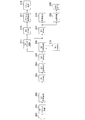
以下、本発明の実施形態について詳細に説明する。本実施形態では、入力画像信号をフレーム期間ごとに処理する画像信号処理装置を撮像装置に適用した例を示す。記録画像用の信号処理回路の一部分から所定の信号(YCC信号)を抜き出して表示用画像処理回路に出力することにより、表示遅延時間を短縮するブロック構成について、ビデオカメラを例にして説明する。 Hereinafter, embodiments of the present invention will be described in detail. In this embodiment, an example in which an image signal processing apparatus that processes an input image signal for each frame period is applied to an imaging apparatus is shown. A block configuration for shortening the display delay time by extracting a predetermined signal (YCC signal) from a part of the recording image signal processing circuit and outputting it to the display image processing circuit will be described by taking a video camera as an example.
まず、本実施形態に係る信号処理装置の構成例について、図1を参照して説明する。
撮像用のセンサ100は、CCD(電荷結合素子)やCMOS(相補型金属酸化膜半導体)等を用いた撮像素子である。図1では省略するが、撮像光学系を構成するレンズ群を通過する被写体光に対して、入射光量や焦点調節が行われる。センサ100は結像された被写体像を光電変換し、内部でアナログ−デジタル変換を行い、各画素の光量に対応したデジタル画像信号を出力する。撮像素子の各画素には、R(赤)、G(緑)、B(青)の各カラーフィルタが、所定の配列、例えばベイヤー配列やハニカム配列で配置されている。これによりRGB画像信号が得られる。また、高速出力化のために、複数の画素の出力を加算して1つの出力画像を得る画素加算処理を行って、RGB画像信号を出力する場合もある。
First, a configuration example of the signal processing apparatus according to the present embodiment will be described with reference to FIG.
The
第1リサイズ処理部101は、センサ100からの入力画像信号(RGB画像信号)を取得して画像縮小処理を行う。縮小するサイズは、第1信号処理部102が処理可能な大きさであり、R(赤)、G(緑)、B(青)の色毎に重心を補正しながら縮小処理が実行される。第1信号処理部102は、RGB画像信号を受信し、RGBのオフセット調整、ゲイン調整、ガンマ補正処理を行う。次に第1信号処理部102は、RGB画像信号から輝度信号(Y)と色差信号(Cb、Cr)へ変換し、YCC画像信号を第1DRAM103に一旦書き込む。
The first
第2信号処理部104は、第1DRAM103からYCC画像信号を読み出す。第2信号処理部104は、YCC画像信号に対して、レンズの歪曲収差の補正処理や、撮像装置の防振処理等を行い、処理後のYCC画像信号を第2DRAM105に書き込む。レンズの歪曲収差の補正は、画像歪の補正処理の一例である。撮像装置の防振処理では手振れ等により生じる像ぶれの補正処理が実行される。第3信号処理部106は、第2DRAM105からYCC画像信号を読み出す。第3信号処理部106は、YCC画像信号に対してノイズリダクション処理等を行い、処理後のYCC画像信号を第3DRAM107に書き込む。その際、第3信号処理部106は、ノイズリダクション機能の実現のために、後述のように、第4DRAM119を併用する。
The second
圧縮伸長部108は、第3DRAM107からYCC画像信号を読み出し、記録フォーマットに合わせて圧縮符号化処理を行う。処理後の信号は記録メディア109に送られて記録される。外部出力部110は、第3DRAM107からYCC画像信号を読み出してフォーマット変換を行う。HDMIやSDI、コンポーネントやコンポジット等の画像信号伝送フォーマットに合わせてフォーマット変換処理が実行される。HDMIは”High-Definition Multimedia Interface”の略号であり、SDIは”Serial Digital Interface”の略号である。フォーマット変換した画像信号は撮像装置外部に出力される。
The compression /
第2リサイズ処理部111は、入力画像信号の画サイズを表示用に変更して第5DRAM112に書き込む画サイズ変更処理を行う。本実施形態の第2リサイズ処理部111は、第1信号処理部102が出力するYCC画像に対して、表示パネルの表示サイズまで縮小する処理を行う。縮小の際、画像のエイリアシングを防止するため、画像の水平方向、垂直方向の各々において帯域制限フィルタにより、画像帯域の制御が行われる。その後、バイキュービック法等の補間手法により、画像の縮小処理が行われ、処理結果は第5DRAM112に記憶される。第4信号処理部113は、第5DRAM112からYCC画像信号を読み出す。第4信号処理部113は、例えばレンズの歪曲収差の補正処理や、撮像装置の防振処理等を行う。処理後のYCC画像信号は第6DRAM114に記憶される。第5信号処理部115は、第6DRAM114からYCC画像信号を読み出す。第5信号処理部115はノイズリダクション処理等を行い、処理後のYCC信号を第7DRAM116に書き込む。その際、第5信号処理部115は、ノイズリダクション機能の実現のために、第8DRAM120を併用する。
The second
パネル用信号処理部117は、画サイズが表示用に変更された画像信号に対して、表示用信号処理を行う。パネル用信号処理部117は、第7DRAM116からパネル表示サイズのYCC画像信号を読み出し、表示パネルに合わせた色の調整処理や、解像度調整処理等を行う。パネル出力部118は、表示パネルの受信フォーマットに合わせてフォーマット変換を行う。フォーマット変換した画像信号は表示パネルに送信されて画面上に画像が表示される。
The panel
次に、本実施形態に対する比較例について、図2を参照して説明する。撮像用のセンサ200の出力信号は第1リサイズ処理部201、第1信号処理部202を経て第1DRAM203に記憶される。第1リサイズ処理部201、第1信号処理部202、第2信号処理部204、第3信号処理部206は、図1の第1リサイズ処理部101、第1信号処理部102、第2信号処理部104、第3信号処理部106にそれぞれ相当する。第2DRAM205、第3DRAM207、第4DRAM219は、図1の第2DRAM105、第3DRAM107、第4DRAM119はそれぞれ相当する。第3信号処理部206の出力する画像信号は2つに分岐し、その一方は第3DRAM207に記憶され、他方は第2リサイズ処理部211に出力される。圧縮伸長部208、記録メディア209、外部出力部210は、図1の圧縮伸長部108、記録メディア109、外部出力部110にそれぞれ相当する。
Next, a comparative example for this embodiment will be described with reference to FIG. The output signal of the
第2リサイズ処理部211は、図1の第2リサイズ処理部111と同じ機能を有する。第2リサイズ処理部211は、圧縮伸長処理以外の全ての記録画像用処理を行った画像に対して画像縮小処理を行い、処理後の画像信号を第5DRAM216に記憶する。パネル用信号処理部217は、第5DRAM216からパネル表示サイズのYCC画像信号を読み出し、表示パネルに合わせた色の調整処理や、解像度調整処理等を行う。パネル出力部218は、表示パネルの受信フォーマットに合わせてフォーマット変換を行う。フォーマット変換した画像信号は表示パネルに送信されて画面上に画像が表示される。
The second
次に、1個のDRAMをアドレス制御によって共用する、本実施形態の構成について説明する。図1では、説明の便宜上、複数のDRAMを個別に使用するブロック構成とした。実際には、DRAMはASIC(Application Specific Integrated Circuit、特定用途向け集積回路)とはプロセスの性質が異なる集積回路であるので、1つのチップに集積せずに別チップ構成にされることも多い。ASICとは別チップとして使用される、1個のDRAMのアドレス制御によって、図1に示す第1ないし第8DRAMの機能を実現できる。この構成について図5を参照して説明する。なお、図5において図1と同じ機能を持つ構成部には、図1で使用した符号と同じ符号を付することにより、それらの詳細な説明を省略する。 Next, the configuration of this embodiment in which one DRAM is shared by address control will be described. In FIG. 1, for convenience of explanation, a block configuration in which a plurality of DRAMs are individually used is used. Actually, DRAM is an integrated circuit having process characteristics different from those of an ASIC (Application Specific Integrated Circuit), so that it is often configured as a different chip without being integrated into one chip. The functions of the first to eighth DRAMs shown in FIG. 1 can be realized by address control of one DRAM used as a separate chip from the ASIC. This configuration will be described with reference to FIG. In FIG. 5, components having the same functions as those in FIG. 1 are given the same reference numerals as those used in FIG. 1, and detailed descriptions thereof are omitted.
DRAM152はDRAM−I/F(インターフェース)部151に接続されている。DRAM−I/F部151には、DRAM152にアクセスしてデータの読み書きを行う各ブロックが接続されている。図5ではスイッチ部150、第2リサイズ処理部111、信号処理aブロック153、信号処理bブロック154、外部出力部110、圧縮伸長部108、パネル用信号処理部117、制御部130がDRAM−I/F部151に接続されている。DRAM−I/F部151は、各ブロックから受けた書き込み要求や読み出し要求を調停し、予め決められた優先順位に従って許可を与える。許可されたブロックは、DRAM152に対して、書き込みを行う場合には、書き込みたいアドレスとデータを所定の長さ分送信する。また、許可されたブロックは、読み出しを行う場合には、読み出したいアドレスを送信し、DRAM152からDRAM−I/F部151を介して所定長さ分のデータを受信する。優先順位が低く、許可を与えられなかったブロックは、優先順位が高いブロックの読み書きが終了するのを待って、順次、データを送受信することができる。
The
第1信号処理部102の出力はスイッチ部150に送られ、ここでは、後述するタイミングに従い、2つの経路に分かれる、第1の経路は、直接DRAM−I/F部151を介してDRAM152にデータを書き込む経路である。また、第2の経路は、第2リサイズ処理部111により、表示パネル140の表示サイズに合わせて画像縮小処理を行ってから、DRAM−I/F部151を介してDRAM152に書き込む経路である。スイッチ部150は制御部130により切り換えられる。
The output of the first
信号処理aブロック153は、図1に示した第2信号処理部104と第4信号処理部113を、時分割で兼用する信号処理ブロックである。このブロックは、例えばレンズの歪曲収差の補正処理や、撮像装置の防振処理等を行う。本ブロックはDRAM−I/F部151と共通の高速クロック信号(例えば166MHz)で動作し、処理する画素数に応じて処理時間が変化する。以下、レンズの歪曲収差の補正処理について、図6を参照して簡単に説明する。図6(A)は画像歪の無い画像の座標を例示し、図6(B)は画像歪を含んだ画像の座標を例示する。
画像歪の無い真の画像座標を(xu,yu)とし、画像歪を含んだ画像座標を(xd,yd)とする。レンズの放射方向の歪みは、下式で表わされる。
The signal processing a
Let true image coordinates without image distortion be (xu, yu), and image coordinates including image distortion be (xd, yd). The distortion in the radial direction of the lens is expressed by the following equation.
[数式1]
xd=(1+k1×r^2+k2×r^4+k3×r^6)×xu
yd=(1+k1×r^2+k2×r^4+k3×r^6)×yu
r^2=xu^2+yu^2 … (1)
ここで、k1、k2、k3は歪み係数であり、レンズとズーム値から定まる。(1)式に示すrは画像中心からの距離である。「^」はべき乗を表わす。
[Formula 1]
xd = (1 + k1 * r ^ 2 + k2 * r ^ 4 + k3 * r ^ 6) * xu
yd = (1 + k1 * r ^ 2 + k2 * r ^ 4 + k3 * r ^ 6) * yu
r ^ 2 = xu ^ 2 + yu ^ 2 (1)
Here, k1, k2, and k3 are distortion coefficients, which are determined from the lens and the zoom value. In the equation (1), r is a distance from the image center. “^” Represents a power.
図6(A)に示す画像歪の無い点601、602、603、604、605はそれぞれ、図6(B)に示す画像歪を含む点611、612、613、614、615に対応している。例えば点601の座標での画素データを求める場合、上式で計算した点611の座標位置での画像データがDRAM152から読み出される。同様に点602の座標での画像データとして、点612の座標位置での画像データが読み出される。こうしてDRAM152から計算結果に該当する座標位置での画像データを順次に読み出していくことで、レンズ歪曲収差を補正した画像が得られる。レンズの歪曲収差の補正処理では、(xu,yu)で示す画像座標の数だけ処理すれば求まるので、処理時間は、処理する画素数にほぼ比例する。また、画像歪について樽型になる場合、図6(B)に示す画像領域は、図6(A)の画像領域よりも若干大きい。このため、やや大きい画像記憶領域を用意する必要がある。
撮像装置に係る防振処理の場合には、図示しない角速度センサや画像認識処理部等により、装置の手振れ量を算出する処理が実行される。撮像画像については、手振れ量に応じた位置に従って、撮影画像領域から所定の範囲を切り出す際の抽出位置を変更する処理が行われ、像ぶれ補正が行われる。この場合、処理時間は、抽出によって生成する画像の画素数にほぼ比例する。
The
In the case of the image stabilization process related to the imaging apparatus, a process for calculating the camera shake amount of the apparatus is executed by an angular velocity sensor, an image recognition processing unit, or the like (not shown). The captured image is subjected to a process of changing the extraction position when a predetermined range is cut out from the captured image area in accordance with the position according to the amount of camera shake, and image blur correction is performed. In this case, the processing time is substantially proportional to the number of pixels of the image generated by extraction.
図5に戻って説明を続ける。信号処理bブロック154は、図1の第3信号処理部106と第5信号処理部115を、時分割で兼用する信号処理ブロックである。このブロックでは、例えばノイズリダクション処理を行う。本ブロックもDRAM−I/F部151と共通の高速クロック信号で動作し、処理する画素数に応じて処理時間が変化する。図7を参照してノイズ低減処理を説明する。図7には具体例として、フレーム巡回型ノイズリダクション回路を示す。
Returning to FIG. The signal
入力端子701から入力されたフレーム画像信号は、第1減算部702と第2減算部703にそれぞれ送られる。第1減算部702のもう一方の端子には、フレームメモリ705から、1フレーム前の同じ位置での画素データが送られてくる。第1減算部702の減算結果は、ノイズ検出及び動き判定部704に送られる。ノイズ検出及び動き判定部704に入力される差分データは、画像に動きが無ければ、ゼロとなる。画像の動きが無い部分で残った残差は、センサ100等で発生したノイズであり、ノイズ検出及び動き判定部704は当該ノイズ成分を第2減算部703に出力する。第2減算部703は、入力端子701から入力されたフレーム画像信号に対して、ノイズ成分を除去し、出力端子706を通じて画像信号を出力するとともに、フレームメモリ705にも出力する。フレームメモリ705は画像信号を記憶し、これは次のフレームで用いられる。ノイズ検出及び動き判定部704に加えられた残差が大きい場合には、画像に動きがあるため、ノイズ検出及び動き判定部704は出力を0に設定する。よって、入力端子701から入力された画像がそのまま出力されるとともに、フレームメモリ705に記憶される。図7の構成例は巡回型であるため、FIFO(First In First Out)として使うフレームメモリが必要であり、処理時間は、処理する画素数にほぼ比例する。
The frame image signal input from the
図5の制御部130は、入力画像信号の同期タイミングと表示用の画像信号の同期タイミングを制御する同期制御部を備える。センサ100の駆動周期と表示パネル140の駆動周期の制御と、遅延時間の制御とが、センサ100と表示パネル140について各々行われる。具体的には、センサ100と表示パネル140の同期信号の遅延量を計測する計測部と、センサ100の駆動周期を基準として、表示パネル140の駆動周期の同期信号に係る遅延量が所定の範囲内に収まるように調節する同期制御部が設けられる。また、各回路部を制御するために、CPU(中央演算処理装置)等の既知の制御ブロックが設けられる。この制御ブロックは、第1ないし第5信号処理部や、パネル用信号処理部117の設定調整等を行う。
The
次に、本実施形態に係る画像信号処理装置の動作について、図3の動作タイミング例を参照して説明する。
本実施形態では、センサ100の駆動周期に対する周波数と、表示パネル140の駆動周期に対応する周波数が等しく24Hzで同期している場合を想定する。同期タイミングについては、図3に示すとおり、センサ同期に比べてパネル同期が遅れたタイミングで同期している。また、センサ100の画素数を8847360ピクセル(水平方向4096ピクセル×垂直方向2160ライン)とし、表示パネル140の画素数を518400ピクセル(水平方向960ピクセル×垂直方向540ライン)とする。信号処理aブロックと信号処理bブロックは、30Hzのプログレッシブの画像を処理できる能力がある。本実施形態では、24Hzの周波数でセンサ100を駆動しているので、各フレーム(1/24秒)に、8847360ピクセルで、1/24−1/30=1/120秒分の処理能力に余裕がある。図3のステップ310ないし320は処理の各過程を表している。
Next, the operation of the image signal processing apparatus according to the present embodiment will be described with reference to the operation timing example of FIG.
In the present embodiment, it is assumed that the frequency corresponding to the driving cycle of the
まず、ステップ(以下、「S」と記す)310において、センサ100はRGB画像信号(水平方向4096ピクセル×垂直方向2160ライン)を出力する。S311において、第1リサイズ処理部101は、センサ100が出力したRGB画像信号を、第1信号処理部102が処理可能な大きさ(水平方向2048ピクセル×垂直方向1080ライン)に縮小する。S312において、第1信号処理部102は、RGB画像信号を輝度信号(Y)と色差信号(Cb、Cr)に変換する。変換したYCC画像信号は、第1DRAM103に記憶されるとともに、第2リサイズ処理部111に送信される。
S313において、S312で第1DRAM103に記憶したYCC画像信号が、S312の処理開始時点から1フレーム期間および1/120秒の時間経過後に読み出され、第2信号処理部104が処理を行う。第2信号処理部104は、レンズの歪曲収差の補正処理や、撮像装置の防振処理等を行い、処理後の画像信号を第2DRAM105に書き込む。ここで、1/120秒分の遅延時間で処理を遅らせる理由は、後述する第4信号処理部113の処理を行うためである(S317参照)。
First, in step (hereinafter referred to as “S”) 310, the
In S313, the YCC image signal stored in the
S314において、S313で第2DRAM105に記憶したYCC画像信号が、S313の処理開始時点から1フレーム期間の時間経過後に読み出され、第3信号処理部106が処理を行う。第3信号処理部106は、フレーム期間内の第1の期間にてノイズリダクション処理を行い、処理後の画像信号(第1画像信号)を第3DRAM107に書き込む。ここで、処理開始時点から約1/120秒の時間が経過した時点で、第3信号処理部106は処理を一時的に中断し、後述する第5信号処理部115の処理を優先させる。フレーム期間内の第2の期間では、第5信号処理部115が処理を行い、処理後の画像信号(第2画像信号)を第7DRAM116に書き込む。第5信号処理部115の処理が終了した後、第3信号処理部106は処理を継続する。この時分割処理の様子を、図8を参照して説明する。
In S314, the YCC image signal stored in the
図8にて点線枠内に示す構成は、フレームメモリ705を除いて図7と同様の機能を有する。同じ機能の部位には図7で使用した同じ符号を付すことで説明を省略する。入力端子701には、選択スイッチ部710を介して第2DRAM105または第6DRAM114からの画像信号が入力される。また、入力端子714には、選択スイッチ部711を介して第4DRAM119または第8DRAM120からの画像信号が入力される。出力端子706は選択スイッチ部712を介して第3DRAM107または第7DRAM116に接続される。また、出力端子715は選択スイッチ部713を介して第4DRAM119または第8DRAM120に接続される。選択スイッチ部710ないし713の各接点に示す「L」は本線系(外部出力および記録信号処理系)のライン選択を表し、「P」はパネル処理系(表示パネル信号処理系)のライン選択を表わす。
The configuration shown in the dotted line frame in FIG. 8 has the same function as in FIG. 7 except for the
ノイズリダクション処理にて、第3信号処理部106が行う本線系の処理の場合、選択スイッチ部710ないし713はL側に切り換る。ノイズリダクション処理後の出力信号は選択スイッチ部712を通じて第3DRAM107に書き込まれる。そして、処理の開始時点から1/120秒の時間が経過した時点で本線系の処理は一旦中断され、選択スイッチ部710ないし713がP側に切り換わり、パネル処理系のノイズリダクション処理が開始する。この切り換え制御は、例えば図示しないCPUの割り込みルーチンにより行われるが、タイマー切り換えでも構わない。パネル処理系の処理する画素数は少ないので、1/120秒以内に処理が終了する。再び、選択スイッチ部710ないし713はL側に切り換わり、前記した本線系の処理を中断したところから処理が続行する。尚、実際には、選択スイッチ部710ないし713による選択制御やDRAM内のアドレス制御については、図示しないCPUがDRAMにアクセスする際のアドレスを変更することにより実現できる。
In the noise reduction processing, in the case of main line processing performed by the third
図3に戻って説明を続ける。S315において、S314で第3DRAM107に記憶されたYCC画像信号(第1画像信号)が、S314の処理開始時点から1フレーム期間の時間経過後に読み出され、外部出力部110が処理を行う。外部出力部110は、所定の画像信号伝送フォーマットに合わせてフォーマット変換を行い、変換した画像信号を撮像装置の外部に出力する。記録処理の場合には、圧縮伸長部108が第3DRAM107からYCC画像信号を読み出して処理し、記録メディア109に画像信号を記録する。
Returning to FIG. 3, the description will be continued. In S315, the YCC image signal (first image signal) stored in the
S312の後、S316で第2リサイズ処理部111は画像縮小処理を行い、表示パネル140の表示サイズ(水平方向960ピクセル×垂直方向540ライン)まで画像を縮小する(水平方向:15/32、垂直方向:1/2)。S317において、信号処理aブロック153(図5参照)を優先して使うことで、レンズの歪曲収差の補正処理や、撮像装置の防振処理等が実行される。S318において、信号処理bブロック154(図5参照)を優先して使うことでノイズリダクション処理が実行される。処理後のYCC画像信号(第2画像信号)は第7DRAM116に記憶される。S319にてパネル用信号処理部117は、S318で第7DRAM116に記憶した画像信号を読み出して、表示パネル140の受信フォーマットに合わせてフォーマット変換を行う。フォーマット変換した画像信号は、S320でパネル出力部118が表示パネル140に送信し、表示パネル140の画面上に画像が表示される。
本実施形態の場合、S310からS320の開始時点まで1フレーム期間強(DL参照)の時間で処理が行われる。
After S312, in S316, the second
In the case of the present embodiment, the process is performed in a time of just over one frame period (see DL) from S310 to the start time of S320.
次に、図2に例示した比較例の動作について、図4の動作タイミング例を参照して説明する。S410ないしS420に処理の各過程を示す。S410でセンサ200の信号読み出しが行われ、S411で第1リサイズ処理部201の処理、S412で第1信号処理部202の処理が行われる。S413ではS412の処理開始時点から1フレーム期間の時間経過後に第2信号処理部204の処理が行われる。さらに1フレーム期間の時間経過後に、S414で第3信号処理部206の処理が行われる。さらに1フレーム期間の時間経過後に、S415で外部出力部210の処理が行われる。S416で第2リサイズ処理部211の処理が行われる。S419でのパネル用信号処理部217の処理と、S420でのパネル出力部218の処理が同時期に実行される。
Next, the operation of the comparative example illustrated in FIG. 2 will be described with reference to the operation timing example of FIG. Each process of processing is shown in S410 to S420. In S410, the signal of the
図2に示す比較例の場合、第2リサイズ処理部211は第3信号処理部206から画像信号を受信して画像縮小処理を行い(図4のS416参照)、処理後の画像信号を第5DRAM216に記憶する。このため、図4のS415の処理と同時期に、S420のパネル出力処理の期間があり、S410から3フレーム期間(DL参照)に相当する表示遅延時間が発生している。これは、フレーム周波数24Hzの場合、約125ミリ秒の表示遅延時間である。
In the case of the comparative example shown in FIG. 2, the second
以上のように、本実施形態によれば、信号処理部の時分割処理によって表示用画像信号の処理を優先させることで、撮影中の画像を表示装置に表示する場合の表示遅延時間を短縮できる。図3のS310からS320まで1フレーム期間強の表示遅延時間であり、図4に示す比較例の3フレーム期間の表示遅延時間に比べて大幅に短縮される。撮影している画像を表示装置に表示する場合の表示遅延時間を短縮することで、表示遅延によるユーザの違和感を解消できる。
また、画像信号の記録処理や出力処理を行う際、信号処理aブロック153および信号処理bブロック154は1/30秒で画像信号を処理する能力を有する。表示用画像信号のフレーム周波数に対応する1/24秒の期間内で1/120秒の隙間ができる。隣接するフレームの画像信号をそれぞれ処理する期間の隙間において、表示用の画像信号に係る第4信号処理部113の処理を優先させることにより、処理効率が高まる。
なお、本実施形態では、撮像用センサの駆動周期と表示パネルの駆動周期を同一にしているので制御が容易になるが、各駆動周期が相違しても構わない。
As described above, according to the present embodiment, by giving priority to the processing of the display image signal by the time division processing of the signal processing unit, it is possible to shorten the display delay time when displaying the image being shot on the display device. . The display delay time is slightly longer than one frame period from S310 to S320 in FIG. 3, which is significantly shorter than the display delay time in the three frame period of the comparative example shown in FIG. By reducing the display delay time when displaying the captured image on the display device, it is possible to eliminate the user's uncomfortable feeling due to the display delay.
Further, when performing image signal recording processing and output processing, the signal processing a
In this embodiment, since the drive cycle of the imaging sensor and the drive cycle of the display panel are the same, control is facilitated, but each drive cycle may be different.
100 センサ(撮像手段)
106 第3信号処理部
110 外部出力部
111 第2リサイズ処理部
115 第5信号処理部
117 パネル用信号処理部
118 パネル出力部
140 表示パネル
152 DRAM
100 sensor (imaging means)
106 third
Claims (7)
前記第1画像信号と前記第2画像信号に対して信号処理を行う信号処理手段と、
前記信号処理手段による信号処理が行われた前記第1画像信号を記録メディアに出力する出力手段と、
前記信号処理手段による信号処理が行われた前記第2画像信号に対して表示用の信号処理を行う表示用信号処理手段を備え、
前記信号処理手段が1フレーム期間を複数の期間に時分割し、1フレーム期間内の異なる期間で前記第1画像信号と前記第2画像信号のそれぞれに対して信号処理を行うことで、前記出力手段が前記第1画像信号を前記記録メディアに出力する前に、前記表示用信号処理手段が前記第1画像信号から生成された前記第2画像信号に対して前記表示用の信号処理を行うことを特徴とする画像信号処理装置。 Resizing processing means for generating a second image signal by reducing the first image signal;
Signal processing means for performing signal processing on the first image signal and the second image signal;
Output means for outputting the first image signal subjected to signal processing by the signal processing means to a recording medium;
Includes a display signal processing hand stage for performing signal processing for display to the second image signal which the signal processing has been performed by the signal processing means,
The signal processing means time-divides one frame period into a plurality of periods, and performs signal processing on each of the first image signal and the second image signal in different periods within one frame period, so that the output The display signal processing means performs the display signal processing on the second image signal generated from the first image signal before the means outputs the first image signal to the recording medium. An image signal processing apparatus.
前記出力手段は前記記憶手段から前記第1画像信号を読み出して前記記録メディアに出力し、The output means reads the first image signal from the storage means and outputs it to the recording medium,
前記表示用信号処理手段は前記記憶手段から前記第2画像信号を読み出して前記表示用の信号処理を行うことを特徴とする請求項1乃至3のいずれか1項に記載の画像信号処理装置。4. The image signal processing apparatus according to claim 1, wherein the display signal processing unit reads the second image signal from the storage unit and performs the display signal processing. 5.
前記撮像手段で生成された第1画像信号を縮小して第2画像信号を生成するサイズ変更処理手段と、
前記第1画像信号と前記第2画像信号に対して信号処理を行う信号処理手段と、
前記信号処理手段による信号処理が行われた前記第1画像信号を記録メディアに出力する出力手段と、
前記信号処理手段による信号処理が行われた前記第2画像信号に対して表示用の信号処理を行う表示用信号処理手段を備え、
前記信号処理手段が1フレーム期間を複数の期間に時分割し、1フレーム期間内の異なる期間で前記第1画像信号と前記第2画像信号のそれぞれに対して信号処理を行うことで、前記出力手段が前記第1画像信号を前記記録メディアに出力する前に、前記表示用信号処理手段が前記第1画像信号から生成された前記第2画像信号に対して前記表示用の信号処理を行うことを特徴とする撮像装置。 Imaging means;
Resizing processing means for reducing the first image signal generated by the imaging means to generate a second image signal ;
Signal processing means for performing signal processing on the first image signal and the second image signal;
Output means for outputting the first image signal subjected to signal processing by the signal processing means to a recording medium;
Includes a display signal processing hand stage for performing signal processing for display to the second image signal which the signal processing has been performed by the signal processing means,
The signal processing means time-divides one frame period into a plurality of periods, and performs signal processing on each of the first image signal and the second image signal in different periods within one frame period, so that the output The display signal processing means performs the display signal processing on the second image signal generated from the first image signal before the means outputs the first image signal to the recording medium. An imaging apparatus characterized by the above.
前記第1画像信号と前記第2画像信号に対して信号処理を行う信号処理ステップと、
前記信号処理ステップにおいて信号処理が行われた前記第1画像信号を記録メディアに出力する出力ステップと、
前記信号処理ステップにおいて信号処理が行われた前記第2画像信号に対して表示用の信号処理を行う表示用信号処理ステップを有し、
前記信号処理ステップにおいて、1フレーム期間を複数の期間に時分割し、1フレーム期間内の異なる期間で前記第1画像信号と前記第2画像信号のそれぞれに対して信号処理を行うことで、前記第1画像信号を前記記録メディアに出力する前に、前記第1画像信号から生成された前記第2画像信号に対して前記表示用の信号処理を行うことを特徴とする画像信号処理装置の制御方法。
A resizing step of reducing the first image signal to generate a second image signal ;
A signal processing step of performing signal processing on the first image signal and the second image signal;
An output step of outputting the first image signal that has undergone signal processing in the signal processing step to a recording medium;
A display signal processing steps for performing signal processing for display to the second image signal which the signal processing is performed in the signal processing step,
In the signal processing step, one frame period is time-divided into a plurality of periods, and signal processing is performed on each of the first image signal and the second image signal in different periods within one frame period, Control of the image signal processing apparatus, wherein the signal processing for display is performed on the second image signal generated from the first image signal before the first image signal is output to the recording medium. Method.
Priority Applications (1)
| Application Number | Priority Date | Filing Date | Title |
|---|---|---|---|
| JP2013000943A JP6091216B2 (en) | 2013-01-08 | 2013-01-08 | Image signal processing apparatus, control method therefor, and imaging apparatus |
Applications Claiming Priority (1)
| Application Number | Priority Date | Filing Date | Title |
|---|---|---|---|
| JP2013000943A JP6091216B2 (en) | 2013-01-08 | 2013-01-08 | Image signal processing apparatus, control method therefor, and imaging apparatus |
Publications (2)
| Publication Number | Publication Date |
|---|---|
| JP2014135537A JP2014135537A (en) | 2014-07-24 |
| JP6091216B2 true JP6091216B2 (en) | 2017-03-08 |
Family
ID=51413550
Family Applications (1)
| Application Number | Title | Priority Date | Filing Date |
|---|---|---|---|
| JP2013000943A Expired - Fee Related JP6091216B2 (en) | 2013-01-08 | 2013-01-08 | Image signal processing apparatus, control method therefor, and imaging apparatus |
Country Status (1)
| Country | Link |
|---|---|
| JP (1) | JP6091216B2 (en) |
Families Citing this family (1)
| Publication number | Priority date | Publication date | Assignee | Title |
|---|---|---|---|---|
| KR102647268B1 (en) * | 2016-09-16 | 2024-03-12 | 소니 세미컨덕터 솔루션즈 가부시키가이샤 | Image pickup device and electronic apparatus |
Family Cites Families (1)
| Publication number | Priority date | Publication date | Assignee | Title |
|---|---|---|---|---|
| JP2009065320A (en) * | 2007-09-05 | 2009-03-26 | Casio Comput Co Ltd | Imaging device |
-
2013
- 2013-01-08 JP JP2013000943A patent/JP6091216B2/en not_active Expired - Fee Related
Also Published As
| Publication number | Publication date |
|---|---|
| JP2014135537A (en) | 2014-07-24 |
Similar Documents
| Publication | Publication Date | Title |
|---|---|---|
| JP5195818B2 (en) | Display control device | |
| US9699384B2 (en) | Image signal processing apparatus and a control method thereof, and an image pickup apparatus and a control method thereof | |
| JP5029725B2 (en) | Imaging device | |
| JP2011249963A (en) | Imaging device | |
| US9363440B2 (en) | Imaging device and imaging method that sets a phase difference between first and second synchronization signals | |
| US9007479B2 (en) | Imaging apparatus and evaluation value generation apparatus | |
| US20240080410A1 (en) | Imaging apparatus, image data processing method of imaging apparatus, and program | |
| KR20100007628A (en) | Image sensor interface apparatus and digital photographing apparatus comprising the same | |
| US8970766B2 (en) | Imaging device | |
| US8908060B2 (en) | Imaging apparatus generating evaluation values at a high frame rate and having a live view function of displaying a video smoothly at a low frame rate | |
| JP5748513B2 (en) | Imaging device | |
| JP6091216B2 (en) | Image signal processing apparatus, control method therefor, and imaging apparatus | |
| JP6955308B2 (en) | Image sensor, image pickup device, image pickup method and program | |
| JP5582229B2 (en) | Camera, display device and image processing device | |
| JP5158165B2 (en) | Imaging device, display timing control circuit | |
| JP2020031336A (en) | Imaging apparatus | |
| JP6087631B2 (en) | Image signal processing apparatus, control method therefor, and imaging apparatus | |
| JP2014154999A (en) | Signal processing device, control method therefor, and control program | |
| JP7334880B2 (en) | METHOD, APPARATUS, PROGRAM, AND RECORDING MEDIUM FOR PROCESSING IMAGE DATA | |
| JP2008066910A (en) | Image processor, image processing method and program | |
| JP6207173B2 (en) | Signal processing apparatus, control method thereof, and control program | |
| WO2020044764A1 (en) | Imaging element, imaging device, image data processing method, and program | |
| JP2004165876A (en) | Image processing apparatus, digital camera, and compound eye system |
Legal Events
| Date | Code | Title | Description |
|---|---|---|---|
| A621 | Written request for application examination |
Free format text: JAPANESE INTERMEDIATE CODE: A621 Effective date: 20151222 |
|
| A977 | Report on retrieval |
Free format text: JAPANESE INTERMEDIATE CODE: A971007 Effective date: 20160823 |
|
| A131 | Notification of reasons for refusal |
Free format text: JAPANESE INTERMEDIATE CODE: A131 Effective date: 20160830 |
|
| A521 | Request for written amendment filed |
Free format text: JAPANESE INTERMEDIATE CODE: A523 Effective date: 20161019 |
|
| TRDD | Decision of grant or rejection written | ||
| A01 | Written decision to grant a patent or to grant a registration (utility model) |
Free format text: JAPANESE INTERMEDIATE CODE: A01 Effective date: 20170110 |
|
| A61 | First payment of annual fees (during grant procedure) |
Free format text: JAPANESE INTERMEDIATE CODE: A61 Effective date: 20170207 |
|
| R151 | Written notification of patent or utility model registration |
Ref document number: 6091216 Country of ref document: JP Free format text: JAPANESE INTERMEDIATE CODE: R151 |
|
| LAPS | Cancellation because of no payment of annual fees |