JP6089492B2 - SYSTEM CONTROL DEVICE, INFORMATION PROCESSING SYSTEM, SYSTEM CONTROL DEVICE CONTROL METHOD, AND SYSTEM CONTROL DEVICE CONTROL PROGRAM - Google Patents
SYSTEM CONTROL DEVICE, INFORMATION PROCESSING SYSTEM, SYSTEM CONTROL DEVICE CONTROL METHOD, AND SYSTEM CONTROL DEVICE CONTROL PROGRAM Download PDFInfo
- Publication number
- JP6089492B2 JP6089492B2 JP2012179905A JP2012179905A JP6089492B2 JP 6089492 B2 JP6089492 B2 JP 6089492B2 JP 2012179905 A JP2012179905 A JP 2012179905A JP 2012179905 A JP2012179905 A JP 2012179905A JP 6089492 B2 JP6089492 B2 JP 6089492B2
- Authority
- JP
- Japan
- Prior art keywords
- component
- access
- access request
- information
- system control
- Prior art date
- Legal status (The legal status is an assumption and is not a legal conclusion. Google has not performed a legal analysis and makes no representation as to the accuracy of the status listed.)
- Expired - Fee Related
Links
Images


Classifications
-
- G—PHYSICS
- G06—COMPUTING; CALCULATING OR COUNTING
- G06F—ELECTRIC DIGITAL DATA PROCESSING
- G06F12/00—Accessing, addressing or allocating within memory systems or architectures
- G06F12/14—Protection against unauthorised use of memory or access to memory
-
- G—PHYSICS
- G06—COMPUTING; CALCULATING OR COUNTING
- G06F—ELECTRIC DIGITAL DATA PROCESSING
- G06F11/00—Error detection; Error correction; Monitoring
- G06F11/22—Detection or location of defective computer hardware by testing during standby operation or during idle time, e.g. start-up testing
- G06F11/26—Functional testing
- G06F11/273—Tester hardware, i.e. output processing circuits
- G06F11/2736—Tester hardware, i.e. output processing circuits using a dedicated service processor for test
-
- G—PHYSICS
- G06—COMPUTING; CALCULATING OR COUNTING
- G06F—ELECTRIC DIGITAL DATA PROCESSING
- G06F11/00—Error detection; Error correction; Monitoring
- G06F11/36—Preventing errors by testing or debugging software
- G06F11/362—Software debugging
- G06F11/3648—Software debugging using additional hardware
- G06F11/3656—Software debugging using additional hardware using a specific debug interface
Landscapes
- Engineering & Computer Science (AREA)
- Theoretical Computer Science (AREA)
- General Engineering & Computer Science (AREA)
- Computer Hardware Design (AREA)
- Physics & Mathematics (AREA)
- General Physics & Mathematics (AREA)
- Quality & Reliability (AREA)
- Computer Security & Cryptography (AREA)
- Bus Control (AREA)
- Information Transfer Systems (AREA)
- Memory System (AREA)
- Debugging And Monitoring (AREA)
Description
本発明は、システム制御装置、情報処理システム、システム制御装置の制御方法およびシステム制御装置の制御プログラムに関する。 The present invention relates to a system control apparatus, an information processing system, a system control apparatus control method, and a system control apparatus control program.
HPC(High Performance Computing)モデルなど、複数のシステムボード(以下SB)をラック等に実装した大規模な計算機システムがある。このような計算機システムは、各SBに多数の部品を高密度に実装することで、設置面積を削減する。 There is a large-scale computer system in which a plurality of system boards (hereinafter referred to as SB) are mounted on a rack or the like such as an HPC (High Performance Computing) model. Such a computer system reduces the installation area by mounting a large number of components on each SB at a high density.
例えば、各SBは、電源制御素子、記憶素子、演算素子および通信素子などの複数の部品を備える。これらの部品は、計算機システムが有するシステム制御装置(サービスプロセッサ、以下SP)によって、システム運用のための制御やデバッグ用途の制御を受ける。 For example, each SB includes a plurality of components such as a power supply control element, a storage element, an arithmetic element, and a communication element. These components are subjected to control for system operation and control for debugging by a system control device (service processor, hereinafter referred to as SP) included in the computer system.
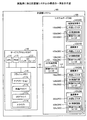
図8を用いて、従来技術に係るSPによる部品の制御について説明する。図8は、従来技術に係るSPおよびSBの構成の一例を示すブロック図である。図8に示すように、計算機システム900は、SP910とSB920とを有する。SP910は、部品制御用のソフトウェア実行部911を有する。SB920は、I2C(Inter-Integrated Circuit、登録商標、以下同様)制御回路921と、電源制御素子922、演算素子923、記憶素子924および通信素子925を有する。なお、電源制御素子922、演算素子923、記憶素子924および通信素子925のことを区別しない場合には、「部品」と称する。
With reference to FIG. 8, control of parts by the SP according to the related art will be described. FIG. 8 is a block diagram showing an example of the SP and SB configurations according to the prior art. As illustrated in FIG. 8, the
I2C制御回路921は、間接アクセス用レジスタ921aを有し、各部品は、I2C制御回路922b〜925bと、内部レジスタ922a〜925aとを有する。また、SP910とSB920との間は、I2Cバス901により接続される。また、SB920において、I2C制御回路921と各部品との間は、I2Cバス902により接続される。
The
SP910のソフトウェア実行部911は、SB920の部品に対する制御を実行する場合、制御用のコマンドをI2C制御回路921に送信する。そして、I2C制御回路921は、ソフトウェア実行部911から受信したコマンドを間接アクセス用レジスタ921aに設定することで、部品に対して制御を実施する。
The
例えば、I2C制御回路921は、演算素子923が有する内部レジスタ923aのアドレス「0x0000_0008」にデータをライトする要求をソフトウェア実行部911から受付けた場合、以下の処理を実行する。すなわち、I2C制御回路921は、間接アクセス用レジスタ921aのアドレスレジスタに、内部レジスタ923aのアドレス「0x0000_0008」をI2Cアクセスでライトする。そして、間接アクセス用レジスタ921aにライトされたアドレスは、演算素子923が有するI2C制御回路923bにより、I2C制御回路923bが有する間接アクセス用レジスタ923cにライトされた後、内部レジスタ923aにライトされる。
For example, when the
I2C制御回路921は、演算素子923が有するI2C制御回路923bからライトの完了を応答された場合、間接アクセス用レジスタ921aのデータレジスタ[63:32]に、ソフトウェア実行部911から受付けたデータをI2Cアクセスでライトする。続いて、I2C制御回路921は、間接アクセス用レジスタ921aのデータレジスタ[31:0]に、ソフトウェア実行部911から受付けたデータをI2Cアクセスでライトする。
When the
この結果、演算素子923が有する内部レジスタ923aのアドレス「0x0000_0008」に、データレジスタ[63:32]、データレジスタ[31:0]の値がライトされる。そして、演算素子923は、内部レジスタ923aのアドレス「0x0000_0008」にデータがライトされたことによる結果をSP910に対して応答する。
As a result, the values of the data register [63:32] and the data register [31: 0] are written to the address “0x0000_0008” of the
しかしながら、上述した従来の技術では、デバッグ時にI2Cアクセスが衝突する場合がある。 However, in the conventional technique described above, there are cases where I2C access collides during debugging.
部品の内部レジスタへのリードあるいはライトは、I2Cでのアクセスが複数回行われる場合がある。また、ハードウェアの初期デバッグ時には、部品制御用のソフトウェアの他に、I2C制御回路921の間接アクセス用レジスタ921aを直接リードあるいはライトするスクリプトが使用される。
There are cases where I2C access is performed a plurality of times for reading or writing to the internal register of the component. In the initial hardware debugging, in addition to the component control software, a script that directly reads or writes the
このため、部品制御用のソフトウェアによるアクセスとスクリプトによるアクセスとが衝突して、部品の内部レジスタに対して正常にリードあるいはライトできない場合がある。 For this reason, there is a case where the access by the component control software and the access by the script collide, and the internal register of the component cannot be normally read or written.
一例として、内部レジスタ923aのアドレス「0x0000_0008」にデータをライトする部品制御用のソフトウェア実行部911と、内部レジスタ923aのアドレス「0x0000_0010」にデータをライトするスクリプトとが衝突する場合をあげる。
As an example, there is a case where a component control
ソフトウェア実行部911が間接アクセス用レジスタ921aのアドレスレジスタに内部レジスタ923aのアドレス「0x0000_0008」をI2Cアクセスでライトする。続いて、スクリプトが間接アクセス用レジスタ921aのアドレスレジスタに内部レジスタ923aのアドレス「0x0000_0010」をI2Cアクセスでライトする。そして、ソフトウェア実行部911が、間接アクセス用レジスタ921aのデータレジスタ[63:32]、データレジスタ[31:0]にライトしたい値をI2Cアクセスでライトすると、内部レジスタ「0x0000_0010」にデータレジスタの値がライトされる。このような場合、SB920において誤動作が起こる。また、部品内の複数ブロックに対して並列的にデバッグを行う場合にも、デバッグ用スクリプト同士が衝突する場合がある。
The
1つの側面では、本発明は、デバッグ時にI2Cアクセスの衝突を防止することができるシステム制御装置、情報処理システム、システム制御装置の制御方法およびシステム制御装置の制御プログラムを提供することを目的とする。 In one aspect, an object of the present invention is to provide a system control apparatus, an information processing system, a system control apparatus control method, and a system control apparatus control program capable of preventing an I2C access collision during debugging. .
本願の開示するシステム制御装置は、一つの態様において、情報処理装置を制御するシステム制御装置であり、発行部と、実行部とを有する。発行部は、情報処理装置が備える部品にアクセスを行う場合、該部品が有するレジスタ内のアドレスを指定するアドレス情報と、該アクセスで該部品にアクセスする回数を示す回数情報とを含むアクセス要求を、該部品に対して発行する。実行部は、部品が他のアクセス要求に含まれる回数情報をカウンタに保持してアクセスごとにカウンタが保持する回数情報を減算してカウンタが保持した回数情報が他のアクセス要求を実行中でないことを示すと判定した結果に基づいてアクセス要求を許可した旨を示す応答を、情報処理装置から受信した場合に、該部品にアクセスする。 In one aspect, a system control device disclosed in the present application is a system control device that controls an information processing device, and includes an issuing unit and an execution unit. When accessing the component included in the information processing apparatus, the issuing unit issues an access request including address information specifying an address in a register included in the component and frequency information indicating the number of times the component is accessed by the access. , Issued for the part. The execution unit holds the number information contained in other access requests in the counter and subtracts the number information held by the counter for each access, and the number information held by the counter is not executing another access request When a response indicating that the access request is permitted is received from the information processing apparatus on the basis of the result of determining that the component is indicated, the component is accessed.
1実施形態におけるシステム制御装置によれば、デバッグ時にI2Cアクセスの衝突を防止することができる。 According to the system control apparatus in one embodiment, collision of I2C access can be prevented during debugging.
以下に、本願の開示するシステム制御装置、情報処理システム、システム制御装置の制御方法およびシステム制御装置の制御プログラムの実施例を図面に基づいて詳細に説明する。なお、この実施例によりこの発明が限定されるものではない。そして、各実施例は、処理内容を矛盾させない範囲で適宜組み合わせることが可能である。 Hereinafter, embodiments of a system control device, an information processing system, a system control device control method, and a system control device control program disclosed in the present application will be described in detail with reference to the drawings. Note that the present invention is not limited to the embodiments. Each embodiment can be appropriately combined within a range in which processing contents are not contradictory.
実施例では、情報処理システムとして、計算機システムを例とする。この計算機システムは、システム制御装置として機能するサービスプロセッサと、情報処理装置として機能するシステムボードとを有する。 In the embodiment, a computer system is taken as an example of the information processing system. This computer system has a service processor that functions as a system control device and a system board that functions as an information processing device.
[実施例に係る計算機システムの構成]
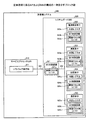
図1を用いて実施例に係る計算機システム100の構成について説明する。図1は、実施例に係る計算機システム100の構成の一例を示す図である。図1に示すように、実施例に係る計算機システム100は、サービスプロセッサ(Service Processor、以下「SP」と記す)110とシステムボード(System Board、以下「SB」と記す)120とを有する。
[Configuration of Computer System According to Embodiment]
A configuration of a computer system 100 according to the embodiment will be described with reference to FIG. FIG. 1 is a diagram illustrating an example of a configuration of a computer system 100 according to the embodiment. As illustrated in FIG. 1, the computer system 100 according to the embodiment includes a service processor (hereinafter referred to as “SP”) 110 and a system board (hereinafter referred to as “SB”) 120.
また、図1に示すように、計算機システム100では、SP110とSB120とがI2C(Inter-Integrated Circuit、登録商標、以下同様)バス101を介して接続する。なお、SP110とSB120との接続はI2Cバスに限定されるものではない。例えば、SP110とSB120との接続は、SPI(Serial Peripheral Interface、登録商標)、MicroWire(登録商標)、IEEE1149.1で規定されるJTAG(Joint Test Architecture Grroup)などの他のバスであってもよい。
As shown in FIG. 1, in the computer system 100, the SP 110 and the SB 120 are connected via an I2C (Inter-Integrated Circuit, registered trademark, hereinafter the same)
[実施例に係るSBの構成]
次に、実施例に係るSBの構成を説明する。図1に示すように、SB120は、I2C制御回路121と、電源制御素子122と、演算素子123と、記憶素子124と、通信素子125とを有する。なお、電源制御素子122、演算素子123、記憶素子124および通信素子125のことを区別しない場合には、「部品200」と称する。また、SB120において、I2C制御回路121と各部品200との間は、I2Cバス102により接続される。
[Configuration of SB according to Example]
Next, the configuration of the SB according to the embodiment will be described. As illustrated in FIG. 1, the SB 120 includes an I2C control circuit 121, a power
ここで、電源制御素子122は、SB120の電源を制御する。演算素子123は、SB120において各種演算処理を実行する。記憶素子124は、SB120で用いられるデータやプログラムを記憶する。通信素子125は、SB120と他装置との情報の送受信を制御する。
Here, the power
また、各部品200は、内部レジスタ203と、I2C制御回路204とを有する。例えば、電源制御素子122は、内部レジスタ122aと、I2C制御回路122bとを有し、演算素子123は、内部レジスタ123aと、I2C制御回路123bとを有する。記憶素子124は、内部レジスタ124aと、I2C制御回路124bとを有し、通信素子125は、内部レジスタ125aと、I2C制御回路125bとを有する。
Each
内部レジスタ203は、アドレスに対応付けて各種の設定値やデータを記憶する。I2C制御回路204は、間接アクセス用レジスタ202を有し、内部レジスタ203とI2C制御回路121との間のデータの読出し、およびデータの書込みを制御する。なお、内部レジスタ203、I2C制御回路204および間接アクセス用レジスタ202の詳細については、図2を用いて後述する。
The
I2C制御回路121は、間接アクセス用レジスタ121aを有し、この間接アクセス用レジスタ121aを介してSP110と各部品200との間のデータの読出し、およびデータの書込みを制御する。なお、間接アクセス用レジスタ121aは、アドレスレジスタ記憶領域(以下、「アドレスレジスタ」と記す)と、データレジスタ記憶領域(以下、「データレスレジスタ」と記す)とを有する。
The I2C control circuit 121 includes an
例えば、I2C制御回路121は、SP110からアクセス要求を受付けた場合、要求された部品200が有するI2C制御回路204にアクセスを許可するか否かを問い合わせる。そして、I2C制御回路121は、アクセスが許可された場合、間接アクセス用レジスタ121aのアドレスレジスタに、アクセスを要求された部品200が有する内部レジスタ203のアドレスを書込む。
For example, when the access request is received from the SP 110, the I2C control circuit 121 inquires whether the access is permitted to the
そして、アクセス要求がリード要求であった場合、部品200が有する内部レジスタ203のアドレスに保持されるデータが、部品200が有するI2C制御回路204を介して、間接アクセス用レジスタ121aのデータレジスタに書込まれる。I2C制御回路121は、SP110からリード要求を受付けた場合、データレジスタに書込まれた値を応答する。
If the access request is a read request, the data held at the address of the
また、I2C制御回路121は、アクセス要求がライト要求であった場合、要求されたデータをSP110から受信する。そして、I2C制御回路121は、間接アクセス用レジスタ121aのデータレジスタに、SP110から受信したデータを書込む。この結果、部品200が有する内部レジスタ203にSP110からライトを要求されたデータが書込まれる。
Further, when the access request is a write request, the I2C control circuit 121 receives the requested data from the SP 110. Then, the I2C control circuit 121 writes the data received from the SP 110 into the data register of the
なお、I2C制御回路121、電源制御素子122、演算素子123、記憶素子124、通信素子125は、ASIC(Application Specific Integrated Circuit)やFPGA(Field Programmable Gate Array)、その他の集積回路である。
The I2C control circuit 121, the power
[実施例に係るSPの構成]
次に、実施例に係るSPの構成を説明する。図1に示すように、SP110は、フラッシュメモリ111と、RAM(Random Access Memory)112と、I2Cインターフェース113と、CPU(Central Processing Unit)114とを有する。
[Configuration of SP according to the embodiment]
Next, the configuration of the SP according to the embodiment will be described. As shown in FIG. 1, the SP 110 includes a flash memory 111, a RAM (Random Access Memory) 112, an I2C interface 113, and a CPU (Central Processing Unit) 114.
フラッシュメモリ111は、アプリケーション111aと、部品ドライバ111bと、I2Cドライバ111cと、スクリプト111dとを記憶する。アプリケーション111aは、各種の業務処理を実行するプログラムである。このアプリケーション111aは、RAM112とCPU114とが協働して実行される。
The flash memory 111 stores an
部品ドライバ111bは、アプリケーション111aにより部品へのアクセス要求を受付けた場合に、要求された部品へのアクセスを制御するプログラムである。この部品ドライバ111bは、RAM112とCPU114とが協働して実行される。これにより、部品ドライバ111bは、処理部300を実現する。
The
例えば、処理部300は、自装置が制御するSB120に備えられる部品200にアクセス要求を発行する場合、以下の処理を実行する。すなわち、処理部300は、部品200が有する内部レジスタ203内のアドレスを指定する情報と、アクセス要求で部品200にアクセスする回数を示す情報とを含めて、部品200へのアクセス要求を発行する。処理部300は、部品200へのアクセス要求が許可されたことを示す応答をSB120から受信した場合に、部品200へアクセスする。なお、部品ドライバ111bにより実現される処理部300の詳細な構成については、図3を用いて後述する。
For example, when the processing unit 300 issues an access request to the
I2Cドライバ111cは、SP110とSB120との間のI2Cアクセスを制御するプログラムである。このI2Cドライバ111cは、RAM112とCPU114とが協働して実行される。これにより、I2Cドライバ111cは、処理部400を実現する。
The I2C driver 111c is a program that controls I2C access between the SP 110 and the SB 120. The I2C driver 111c is executed in cooperation with the
例えば、処理部400は、部品ドライバ111bからコマンドを受付けた場合、間接アクセス用レジスタ121aにアクセスを実行する。そして、処理部400は、I2C制御回路204から受信した応答がACK応答である場合、ACK応答を部品ドライバ111bに応答する。一方、処理部400は、I2C制御回路204から受信した応答がNACK応答である場合、NACK応答を部品ドライバ111bに応答する。
For example, when receiving a command from the
スクリプト111dは、デバッグ時にアプリケーション111aや部品ドライバ111bとは独立してI2Cドライバ111cを制御するプログラムである。このスクリプト111dは、RAM112とCPU114とが協働して実行される。これにより、スクリプト111dは、処理部500を実現する。
The script 111d is a program that controls the I2C driver 111c independently of the
例えば、処理部500は、自装置が制御するSB120に備えられる部品にアクセスを行う場合、以下の処理を実行する。すなわち、処理部500は、部品200が有する内部レジスタ203内のアドレスを指定するアドレス情報と、このアクセスで部品200にアクセスする回数を示す回数情報とを含むアクセス要求を、部品200に対して発行する。処理部500は、部品200がアクセス要求を許可した旨を示す応答を、SB120から受信した場合に、部品200にアクセスする。
For example, the processing unit 500 executes the following processing when accessing a component provided in the SB 120 controlled by the own device. That is, the processing unit 500 issues an access request including address information for specifying an address in the
RAM112は、CPU114がフラッシュメモリ111から読出したアプリケーション111a、部品ドライバ111b、I2Cドライバ111c及びスクリプト111dを記憶する。
The
I2Cインターフェース113は、I2CコマンドをSB120に送信する。また、I2Cインターでフェース113は、I2CコマンドをSB120から受信する。CPU114は、各種演算処理を実行するとともに、フラッシュメモリ111が記憶するアプリケーション111a、部品ドライバ111b、I2Cドライバ111c及びスクリプト111dを実行する。
The I2C interface 113 transmits an I2C command to the SB 120. Further, the interface 113 receives an I2C command from the SB 120 through the I2C interface. The
[部品200の構成]
次に、図2を用いて、部品200の構成を説明する。図2は、部品200の構成の一例を示す図である。図2に示すように、部品200は、アクセス回数カウンタ201と、間接アクセス用レジスタ202と、内部レジスタ203と、I2C制御回路204とを有する。
[Configuration of Part 200]
Next, the configuration of the
内部レジスタ203は、アドレスに対応付けて各種の設定値やデータを記憶する。図2に示すように、内部レジスタ203は、アドレスごとに64ビットのデータを記憶する。
The
アクセス回数カウンタ201は、アクセス要求を許可されたSP110によってアクセス要求に含められた回数情報に対応する回数を保持する。言い換えると、アクセス回数カウンタ201は、アクセス要求を許可されたSP110が、アクセス要求でアクセスする回数を保持する。アクセス回数カウンタ201が保持するアクセスする回数は、SP110によりアクセスが実行されるごとに減算される。
The
間接アクセス用レジスタ202は、アドレスレジスタと、データレジスタ[63:32]と、データレジスタ[31:0]とを有する。アドレスレジスタには、SP110からアクセスを要求される部品200の内部レジスタ203のアドレスが格納される。ここで、アドレスレジスタの下位3ビットがアクセス回数セット部として用いられる。
The
データレジスタ[63:32]は、アクセスを要求された内部レジスタ203のアドレスに書込まれるデータあるいは、アクセスを要求された内部レジスタ203のアドレスから読出されたデータのうち、63ビット目から32ビット目の値が格納される。データレジスタ[31:0]は、アクセスを要求された内部レジスタ203のアドレスに書込まれるデータあるいは、アクセスを要求された内部レジスタ203のアドレスから読出されたデータのうち、31ビット目から0ビット目の値が格納される。
The data register [63:32] is 32 bits from the 63rd bit among the data written to the address of the
I2C制御回路204は、I2Cリード要求またはI2Cライト要求を、I2C制御回路121を介してSP110から受信し、受信したリード要求またはライト要求に対して応答する。
The
例えば、I2C制御回路204は、アクセス要求をSP110から受信した場合、アクセス回数カウンタ201が保持した回数が、受信したアクセス要求以外のアクセスを実行中ではないことを示すかを判定する。言い換えると、I2C制御回路204は、アクセス回数カウンタ201の保持する値が他のアクセスを実行中ではないことを示す情報であるか否かを判定する。例えば、I2C制御回路204は、アクセス回数カウンタ201の保持する値が「0」であるか否かを判定する。そして、I2C制御回路204は、アクセス回数カウンタ201の保持する値が「0」である場合、他のアクセスが実行中ではないと判定する。一方、I2C制御回路204は、アクセス回数カウンタ201の保持する値が「0」ではない場合、他のアクセスが実行中であると判定する。
For example, when an access request is received from the SP 110, the
そして、I2C制御回路204は、判定結果に基づき、アクセス要求を許可する旨又はアクセス要求を許可しない旨を応答する。I2C制御回路204は、他のアクセスを実行中ではないと判定する場合、アクセス要求を許可する旨を示すACK応答を応答するとともに、アクセス要求に含まれるアクセス回数をアクセス回数カウンタ201に保持させる。
Based on the determination result, the
また、I2C制御回路204は、間接アクセス用レジスタ202にアドレスを設定する。ここで、アクセス要求がリード要求である場合、設定した内部レジスタ203のアドレスに保持されるデータが間接アクセス用レジスタ202に格納される。そして、I2C制御回路204は、リードアクセスが実行されると、間接アクセス用レジスタ202に格納されるデータをSP110に応答する。
The
また、I2C制御回路204は、アクセス要求がライト要求である場合に、ライトアクセスが実行されると、SP110からデータを受信し、間接アクセス用レジスタ202に受信したデータを格納する。これにより、間接アクセス用レジスタ202に格納されたデータが、内部レジスタ203に書込まれる。
When the access request is a write request and the write access is executed, the
また、I2C制御回路204は、SP110からアクセスされるごとに、アクセス回数カウンタ201が保持した回数を減算する。言い換えると、I2C制御回路204は、SP110からリードアクセスまたはライトアクセスが実行されるごとに、アクセス回数カウンタ201に保持される回数を減算する。
Further, every time the
また、I2C制御回路204は、他のアクセスを実行中であると判定する場合、アクセス要求を許可しない旨を示すNACK応答を応答する。
If the
[部品ドライバ111bにより実現される処理部300の機能構成]
次に、図3を用いて、実施例1に係るSP110により部品ドライバ111bを用いて実現される処理部の機能構成を説明する。図3は、SP110により部品ドライバ111bを用いて実現される処理部の機能構成を示す機能ブロック図である。なお、SP110により実行される部品ドライバ111bは、RAM112と、CPU114とが協働して実現される。
[Functional Configuration of Processing Unit 300 Realized by
Next, the functional configuration of the processing unit realized by the SP 110 according to the first embodiment using the
図3に示すように、部品ドライバ111bにより実現される処理部300は、要求受付部301と、コマンド発行部302と、応答判定部303と、コマンド実行部304とを有する。
As illustrated in FIG. 3, the processing unit 300 realized by the
要求受付部301は、部品200の内部レジスタ203からデータを読出す要求であるリード要求または部品200の内部レジスタ203にデータを書込む要求であるライト要求をアプリケーション111aから受付ける。そして、要求受付部301は、コマンド発行部302にアクセス要求の発行を依頼する。
The
コマンド発行部302は、SB120が備える部品200にアクセスを行う場合、以下の処理を実行する。すなわち、コマンド発行部302は、部品200が有するレジスタ内のアドレスを指定するアドレス情報と、このアクセスで部品200にアクセスする回数を示す回数情報とを含むアクセス要求を、部品200に対して発行する。
The
例えば、コマンド発行部302は、アクセスがリードアクセスであるかライトアクセスであるかを示す情報をコマンドに含める。また、コマンド発行部302は、アドレスを指定する情報の一部を、回数を示す情報に用いる。一例をあげると、コマンド発行部302は、アドレスを指定する情報の下位の2ビットまたは3ビットを用いて、アクセスする回数を示す情報を指定する。なお、ここでは、下位の3ビットを用いて、アクセスする回数を示す情報を指定するものとして説明する。
For example, the
応答判定部303は、I2Cドライバ111cから受信する応答がACK応答であるかNACK応答であるかを判定する。応答判定部303は、I2Cドライバ111cから受信する応答がACK応答であると判定する場合、コマンド実行部304にアクセスの実行を依頼する。
The
また、応答判定部303は、I2Cドライバ111cから受信する応答がNACK応答であると判定する場合、コマンド発行部302にアクセス要求の再発行を依頼する。この結果、コマンド発行部302は、アドレス情報と回数情報とを含むアクセス要求を再発行する。
If the
コマンド実行部304は、リード制御部305と、ライト制御部306とを有し、部品200がアクセス要求を許可した旨を示す応答を、SB120から受信した場合に、部品200にアクセスする。
The
リード制御部305は、アプリケーション111aからリード要求を受信した場合、I2Cドライバ111cにリードアクセスの実行を依頼して、部品200の内部レジスタ203からデータを読出す。そして、リード制御部305は、読出したデータをアプリケーション111aに応答する。
When the read
ライト制御部306は、アプリケーション111aからライト要求を受信した場合、ライトデータを受信する。そして、ライト制御部306は、I2Cドライバ111cに受信したデータのライトアクセスを依頼する。
The
[部品ドライバ111bにより実現される処理部300による処理の処理手順]
次に図4および図5を用いて、部品ドライバ111bにより実現される処理部300による処理の処理手順を説明する。ここでは、図4を用いて、リード処理を説明し、図5を用いて、ライト処理を説明する。
[Processing Procedure of Processing by Processing Unit 300 Realized by
Next, a processing procedure of processing by the processing unit 300 realized by the
(リード処理)
図4は、部品ドライバ111bにより実現される処理部300によるリード処理の処理手順を示すフローチャートである。図4に示すように、要求受付部301は、部品200の内部レジスタ203からデータを読出す要求であるリード要求をアプリケーション111aから受付けたか否かを判定する(ステップS101)。コマンド発行部302は、リード要求をアプリケーション111aから受付けたと要求受付部301により判定される場合(ステップS101、Yes)、アクセス回数をアドレスに含めたアクセス要求コマンドを生成する(ステップS102)。
(Lead processing)
FIG. 4 is a flowchart showing a processing procedure of read processing by the processing unit 300 realized by the
そして、コマンド発行部302は、生成したアクセス要求コマンドを送信する(ステップS103)。続いて、応答判定部303は、アクセス許可を受信したか否かを判定する(ステップS104)。ここで、コマンド発行部302は、アクセス許可を受信していないと応答判定部303により判定された場合(ステップS104、No)、ステップS103に移行してアクセス要求コマンドを送信する。
Then, the
リード制御部305は、アクセス許可を受信したと応答判定部303により判定された場合(ステップS104、Yes)、部品200の内部レジスタ203からデータを読出すリード要求をI2Cドライバ111cに実行する(ステップS105)。そして、リード制御部305は、部品200の内部レジスタ203から読出されたリードデータをI2Cドライバ111cから受信する(ステップS106)。
When the
続いて、リード制御部305は、要求したデータのうち未受信のデータがあるか否かを判定する(ステップS107)。ここで、リード制御部305は、要求したデータのうち未受信のデータがあると判定する場合(ステップS107、Yes)、ステップS105に移行して、部品200の内部レジスタ203から読出されたリードデータをI2Cドライバ111cから受信する。
Subsequently, the
リード制御部305は、要求したデータのうち未受信のデータがないと判定する場合(ステップS107、No)、部品200の内部レジスタ203から読出されたリードデータをアプリケーション111aに応答し(ステップS108)、リード処理を終了する。
If the
なお、要求受付部301は、リード要求をアプリケーションから受付けていないと判定する場合(ステップS101、No)、引き続き、リード要求をアプリケーション111aから受付けたか否かを判定する。
When determining that the read request is not received from the application (No in step S101), the
(ライト処理)
図5は、部品ドライバ111bにより実現される処理部300によるライト処理の処理手順を示すフローチャートである。図5に示すように、要求受付部301は、部品200の内部レジスタ203にデータを書込む要求であるライト要求をアプリケーション111aから受付けたか否かを判定する(ステップS201)。そして、要求受付部301は、アプリケーション111aからライト要求を受付けたと判定する場合(ステップS201、Yes)、ライトデータをアプリケーション111aから受信する(ステップS202)。
(Light processing)
FIG. 5 is a flowchart showing the processing procedure of the write processing by the processing unit 300 realized by the
続いて、コマンド発行部302は、アクセス回数をアドレスに含めたアクセス要求コマンドを生成する(ステップS203)。
Subsequently, the
そして、コマンド発行部302は、生成したアクセス要求コマンドを送信する(ステップS204)。続いて、応答判定部303は、アクセス許可を受信したか否かを判定する(ステップS205)。ここで、コマンド発行部302は、アクセス許可を受信していないと応答判定部303により判定された場合(ステップS205、No)、ステップS204に移行してアクセス要求コマンドを送信する。
Then, the
ライト制御部306は、アクセス許可を受信したと応答判定部303により判定された場合(ステップS205、Yes)、部品200の内部レジスタ203にライトデータを書込むライト要求をI2Cドライバ111cに実行する(ステップS206)。
If the
続いて、ライト制御部306は、ライト要求したデータのうち未送信のデータがあるか否かを判定する(ステップS207)。ここで、ライト制御部306は、要求したデータのうち未送信のデータがあると判定する場合(ステップS207、Yes)、ステップS206に移行して、部品200の内部レジスタ203にライトデータを書込むライト要求をI2Cドライバ111cに実行する。
Subsequently, the
ライト制御部306は、要求したデータのうち未送信のデータがないと判定する場合(ステップS207、No)、ライトデータの書込みが完了したことをアプリケーション111aに応答し(ステップS208)、ライト処理を終了する。
If the
なお、要求受付部301は、ライト要求をアプリケーション111aから受付けていないと判定する場合(ステップS201、No)、引き続き、ライト要求をアプリケーション111aから受付けたか否かを判定する。
When it is determined that the write request is not received from the
[I2Cドライバ111cにより実現される処理部400による処理の処理手順]
次に図6を用いて、I2Cドライバ111cにより実現される処理部400による処理の処理手順を説明する。図6は、I2Cドライバ111cにより実現される処理部400による処理の処理手順を示すフローチャートである。
[Processing Procedure of Processing by Processing Unit 400 Realized by I2C Driver 111c]
Next, a processing procedure of processing by the processing unit 400 realized by the I2C driver 111c will be described with reference to FIG. FIG. 6 is a flowchart illustrating a processing procedure of processing performed by the processing unit 400 realized by the I2C driver 111c.
処理部400は、部品ドライバ111bからコマンドを受付けたか否かを判定する(ステップS301)。ここで、処理部400は、部品ドライバ111bからコマンドを受付けたと判定する場合(ステップS301、Yes)、間接アクセス用レジスタ121aにアクセスを実行する(ステップS302)。
The processing unit 400 determines whether a command has been received from the
そして、処理部400は、I2C制御回路204から応答を受信する(ステップS303)。続いて、処理部400は、I2C制御回路204から受信した応答がACK応答であるか否かを判定する(ステップS304)。ここで、処理部400は、I2C制御回路204から受信した応答がACK応答であると判定する場合(ステップS304、Yes)、ACK応答を部品ドライバ111bに応答し(ステップS305)、処理を終了する。
Then, the processing unit 400 receives a response from the I2C control circuit 204 (step S303). Subsequently, the processing unit 400 determines whether or not the response received from the
一方、処理部400は、I2C制御回路204から受信した応答がACK応答ではないと判定する場合(ステップS304、No)、NACK応答を部品ドライバ111bに応答し(ステップS306)、処理を終了する。
On the other hand, if the processing unit 400 determines that the response received from the
[I2C制御回路204による処理の処理手順]
次に図7を用いて、I2C制御回路204による処理の処理手順を説明する。図7は、I2C制御回路204による処理の処理手順を示すフローチャートである。
[Processing Procedure of I2C Control Circuit 204]
Next, a processing procedure of processing by the
図7に示すように、I2C制御回路204は、I2Cドライバ111cからコマンドを受信したか否かを判定する(ステップS401)。ここで、I2C制御回路204は、I2Cドライバ111cからコマンドを受信したと判定する場合(ステップS401、Yes)、受信したコマンドがアドレス設定要求であるか否かを判定する(ステップS402)。
As shown in FIG. 7, the
I2C制御回路204は、受信したコマンドがアドレス設定要求であると判定する場合(ステップS402、Yes)、アクセス回数カウンタ201のカウント値が0であるか否かを判定する(ステップS403)。例えば、I2C制御回路204は、カウント値セット信号をアクセスカウンタ201に入力する。
When determining that the received command is an address setting request (Yes in step S402), the
そして、I2C制御回路204は、アクセス回数カウンタ201のカウント値が0ではないと判定する場合(ステップS403、No)、NACK応答をI2Cドライバ111cに応答する(ステップS404)。
If the
また、I2C制御回路204は、アクセス回数カウンタ201のカウント値が0であると判定する場合(ステップS403、Yes)、間接アクセス用レジスタ202にアドレスを設定する(ステップS405)。続いて、I2C制御回路204は、アクセス回数カウンタ201にカウント値を設定し(ステップS406)、ACK応答をI2Cドライバ111cに応答する(ステップS407)。
If the
I2C制御回路204は、受信したコマンドがアドレス設定要求ではないと判定する場合(ステップS402、No)、受信したコマンドがリード要求であるか否かを判定する(ステップS408)。I2C制御回路204は、受信したコマンドがリード要求であると判定する場合(ステップS408、Yes)、データを読出す(ステップS409)。そして、I2C制御回路204は、アクセス回数カウンタ201にカウント値減算信号を入力する(ステップS410)。I2C制御回路204は、ステップS410の処理の終了後、ステップS407を実行する。
When determining that the received command is not an address setting request (No in step S402), the
I2C制御回路204は、受信したコマンドがリード要求ではないと判定する場合(ステップS408、No)、データを書込む(ステップS411)。I2C制御回路204は、ステップS411の処理の終了後、ステップS410を実行する。また、I2C制御回路204は、ステップS404の処理の終了後またはステップS407の処理の終了後、処理を終了する。
If the
[実施例の効果]
上述してきたように、実施例に係るSP110は、同一の部品200に対する複数のI2Cアクセスの衝突を防止することができる。例えば、実施例に係るSP110は、ハードウェアの初期デバッグ用スクリプトとシステムボート制御用のファームウェアとを衝突を考慮せずにアクセスが可能となる。
[Effect of Example]
As described above, the SP 110 according to the embodiment can prevent a plurality of I2C access collisions with respect to the
また、本実施例において説明した各処理のうち自動的に行われるものとして説明した処理の全部または一部を手動的に行うこともできる。あるいは、手動的に行われるものとして説明した処理の全部又は一部を公知の方法で自動的に行うこともできる。この他、上記文章中や図面中で示した処理手順、制御手順、具体的名称については、特記する場合を除いて任意に変更することができる。また、各種の負荷や使用状況などに応じて、各実施例において説明した各処理の各ステップでの処理の順番を変更してもよい。 In addition, all or a part of the processes described as being automatically performed among the processes described in the present embodiment can be manually performed. Alternatively, all or part of the processing described as being performed manually can be automatically performed by a known method. In addition, the processing procedures, control procedures, and specific names shown in the text and drawings can be arbitrarily changed unless otherwise specified. Further, the order of processing in each step of each processing described in each embodiment may be changed according to various loads and usage conditions.
また、図示した各構成部は、機能概念的なものであり、必ずしも物理的に図示のごとく構成されることを要しない。例えば、処理部300では、要求受付部301とコマンド発行部302とが統合されてもよい。さらに、各装置にて行われる各処理機能は、その全部または任意の一部が、CPUおよび当該CPUにて解析実行されるプログラムにて実現され、あるいは、ワイヤードロジックによるハードウェアとして実現され得る。
Each illustrated component is functionally conceptual and does not necessarily need to be physically configured as illustrated. For example, in the processing unit 300, the
以上の実施例を含む実施形態に関し、さらに以下の付記を開示する。 The following supplementary notes are further disclosed with respect to the embodiments including the above examples.
(付記1)情報処理装置を制御するシステム制御装置において、
前記情報処理装置が備える部品にアクセスを行う場合、該部品が有するレジスタ内のアドレスを指定するアドレス情報と、該アクセスで該部品にアクセスする回数を示す回数情報とを含むアクセス要求を、該部品に対して発行する発行部と、
前記部品が前記アクセス要求を許可した旨を示す応答を、前記情報処理装置から受信した場合に、該部品にアクセスする実行部と
を有することを特徴とするシステム制御装置。
(Additional remark 1) In the system control apparatus which controls information processing apparatus,
When accessing a component included in the information processing apparatus, an access request including address information specifying an address in a register included in the component and frequency information indicating the number of times the component is accessed by the access An issuer to issue to
And an execution unit that accesses the component when receiving a response indicating that the component has permitted the access request from the information processing device.
(付記2)前記発行部は、前記アドレスを指定する情報の一部を、前記回数を示す情報に用いることを特徴とする付記1に記載のシステム制御装置。
(Additional remark 2) The said issuing part uses a part of information which designates the said address for the information which shows the said frequency | count, The system control apparatus of
(付記3)前記発行部は、前記部品へのアクセス要求が許可されなかった旨を示す応答を、前記情報処理装置から受信した場合に、前記アドレス情報と前記回数情報とを含むアクセス要求を再発行することを特徴とする付記1または2に記載のシステム制御装置。
(Supplementary Note 3) When the issuing unit receives a response indicating that the access request to the component is not permitted from the information processing apparatus, the issuing unit re-issues the access request including the address information and the frequency information. The system control apparatus according to
(付記4)アクセス要求を許可された前記システム制御装置によって該アクセス要求に含められた前記回数情報に対応する回数を保持するカウンタと、
前記システム制御装置からアクセスされるごとに、前記カウンタが保持した回数を減算する減算部と、
アクセス要求を前記システム制御装置から受信した場合、前記カウンタが保持した回数が、該受信したアクセス要求以外のアクセスを実行中ではないことを示すかを判定する判定部と、
前記判定部による判定結果に基づき、前記アクセス要求を許可する旨又は前記アクセス要求を許可しない旨を応答する応答部と
を有することを特徴とする被制御装置。
(Supplementary Note 4) A counter that holds the number of times corresponding to the number of times included in the access request by the system control device that has been granted the access request;
A subtraction unit that subtracts the number of times held by the counter each time it is accessed from the system control device;
When receiving an access request from the system control device, a determination unit that determines whether the number of times held by the counter indicates that an access other than the received access request is not being executed;
And a response unit that responds to permit the access request or not to permit the access request based on a determination result by the determination unit.
(付記5)情報処理装置と、該情報処理装置を制御するシステム制御装置とを有する情報処理システムにおいて、
前記システム制御装置は、
前記情報処理装置が備える部品にアクセスを行う場合、該部品が有するレジスタ内のアドレスを指定するアドレス情報と、該アクセスで該部品にアクセスする回数を示す回数情報とを含むアクセス要求を、該部品に対して発行する発行部と、
前記部品が前記アクセス要求を許可した旨を示す応答を、前記システム制御装置が、前記情報処理装置から受信した場合に、該部品にアクセスする実行部とを有し、
前記情報処理装置が備える部品は、
アクセス要求を許可された前記システム制御装置によって該アクセス要求に含められた前記回数情報に対応する回数を保持するカウンタと、
前記システム制御装置からアクセスされるごとに、前記カウンタが保持した回数を減算する減算部と、
アクセス要求を前記システム制御装置から受信した場合、前記カウンタが保持した回数が、該受信したアクセス要求以外のアクセスを実行中ではないことを示すかを判定する判定部と、
前記判定部による判定結果に基づき、前記アクセス要求を許可する旨又は前記アクセス要求を許可しない旨を応答する応答部とを有する
ことを特徴とする情報処理システム。
(Additional remark 5) In the information processing system which has information processing apparatus and the system control apparatus which controls this information processing apparatus,
The system controller is
When accessing a component included in the information processing apparatus, an access request including address information specifying an address in a register included in the component and frequency information indicating the number of times the component is accessed by the access An issuer to issue to
An execution unit that accesses the component when the system control device receives a response indicating that the component has permitted the access request from the information processing device;
The components included in the information processing apparatus are:
A counter that holds the number of times corresponding to the number of times information included in the access request by the system control device that has been granted the access request;
A subtraction unit that subtracts the number of times held by the counter each time it is accessed from the system control device;
When receiving an access request from the system control device, a determination unit that determines whether the number of times held by the counter indicates that an access other than the received access request is not being executed;
An information processing system comprising: a response unit that responds that the access request is permitted or the access request is not permitted based on a determination result by the determination unit.
(付記6)情報処理装置を制御するシステム制御装置の制御方法において、
前記システム制御装置が有する発行部が、前記情報処理装置が備える部品にアクセスを行う場合、前記発行部が、該部品が有するレジスタ内のアドレスを指定するアドレス情報と、該アクセスで該部品にアクセスする回数を示す回数情報とを含むアクセス要求を、該部品に対して発行し、
前記部品が前記アクセス要求を許可した旨を示す応答を、前記システム制御装置が、前記情報処理装置から受信した場合に、前記システム制御装置が有する実行部が、該部品にアクセスすることを特徴とするシステム制御装置の制御方法。
(Supplementary note 6) In a control method of a system control device for controlling an information processing device,
When the issuing unit included in the system control device accesses a component included in the information processing device, the issuing unit accesses the component using address information that specifies an address in a register included in the component, and the access. Issue an access request including the number of times information indicating the number of times to the component,
When the system control apparatus receives a response indicating that the component permits the access request from the information processing apparatus, the execution unit of the system control apparatus accesses the component. Control method for system control device.
(付記7)前記発行する処理は、前記アドレスを指定する情報の一部を、前記回数を示す情報に用いることを特徴とする付記6に記載のシステム制御装置の制御方法。 (Supplementary note 7) The control method of the system control device according to supplementary note 6, wherein the issuing process uses a part of information specifying the address as information indicating the number of times.
(付記8)前記発行する処理は、前記部品へのアクセス要求が許可されなかった旨を示す応答を、前記情報処理装置から受信した場合に、前記アドレス情報と前記回数情報とを含むアクセス要求を再発行することを特徴とする付記6または7に記載のシステム制御装置の制御方法。 (Supplementary Note 8) When the process to be issued receives a response indicating that an access request to the component has not been permitted from the information processing apparatus, the process to issue an access request including the address information and the frequency information The control method of the system control device according to appendix 6 or 7, wherein reissue
(付記9)情報処理装置を制御するシステム制御装置の制御プログラムにおいて、
前記システム制御装置が有する発行部が、前記情報処理装置が備える部品にアクセスを行う場合、前記発行部に、該部品が有するレジスタ内のアドレスを指定するアドレス情報と、該アクセスで該部品にアクセスする回数を示す回数情報とを含むアクセス要求を、該部品に対して発行させ、
前記部品が前記アクセス要求を許可した旨を示す応答を、前記システム制御装置が、前記情報処理装置から受信した場合に、前記システム制御装置が有する実行部に、該部品にアクセスさせることを特徴とするシステム制御装置の制御プログラム。
(Supplementary note 9) In a control program of a system control device for controlling an information processing device,
When the issuing unit included in the system control device accesses a component included in the information processing device, the issuing unit accesses the component by address information specifying an address in a register included in the component and the access. An access request including the number of times information indicating the number of times to be issued to the component,
When the system control device receives a response indicating that the component permits the access request from the information processing device, the execution unit of the system control device causes the component to access the component. Control program for the system controller.
(付記10)前記発行する処理は、前記アドレスを指定する情報の一部を、前記回数を示す情報に用いることを特徴とする付記9に記載のシステム制御装置の制御プログラム。 (Supplementary note 10) The control program for the system control device according to supplementary note 9, wherein the issuing process uses a part of information designating the address as information indicating the number of times.
(付記11)前記発行する処理は、前記部品へのアクセス要求が許可されなかった旨を示す応答を、前記情報処理装置から受信した場合に、前記アドレス情報と前記回数情報とを含むアクセス要求を再発行することを特徴とする付記9または10に記載のシステム制御装置の制御プログラム。 (Supplementary Note 11) When the process to be issued receives a response indicating that an access request to the component has not been permitted from the information processing apparatus, an access request including the address information and the frequency information is received. 11. The control program for a system control device according to appendix 9 or 10, wherein re-issue
100 計算機システム
101、102 I2Cバス
110 SP
111 フラッシュメモリ
111a アプリケーション
111b 部品ドライバ
111c I2Cドライバ
111d スクリプト
112 RAM
113 I2Cインターフェース
114 CPU
120 SB
121 I2C制御回路
121a 間接アクセス用レジスタ
122 電源制御素子
123 演算素子
124 記憶素子
125 通信素子
200 部品
201 アクセス回数カウンタ
202 間接アクセス用レジスタ
203 内部レジスタ
204 I2C制御回路
300、400、500 処理部
301 要求受付部
302 コマンド発行部
303 応答判定部
304 コマンド実行部
305 リード制御部
306 ライト制御部
100
111
113
120 SB
121
Claims (6)
前記情報処理装置が備える部品にアクセスを行う場合、該部品が有するレジスタ内のアドレスを指定するアドレス情報と、該アクセスで該部品にアクセスする回数を示す回数情報とを含むアクセス要求を、該部品に対して発行する発行部と、
前記部品が他のアクセス要求に含まれる回数情報をカウンタに保持してアクセスごとにカウンタが保持する回数情報を減算してカウンタが保持した回数情報が他のアクセス要求を実行中でないことを示すと判定した結果に基づいて前記アクセス要求を許可した旨を示す応答を、前記情報処理装置から受信した場合に、該部品にアクセスする実行部と
を有することを特徴とするシステム制御装置。 In a system control device that controls an information processing device,
When accessing a component included in the information processing apparatus, an access request including address information specifying an address in a register included in the component and frequency information indicating the number of times the component is accessed by the access An issuer to issue to
When the component holds the number information contained in the other access request in the counter and subtracts the number information held by the counter for each access, the number information held by the counter indicates that the other access request is not being executed. A system control apparatus comprising: an execution unit that accesses the component when a response indicating that the access request is permitted based on the determined result is received from the information processing apparatus.
前記システム制御装置は、
前記情報処理装置が備える部品にアクセスを行う場合、該部品が有するレジスタ内のアドレスを指定するアドレス情報と、該アクセスで該部品にアクセスする回数を示す回数情報とを含むアクセス要求を、該部品に対して発行する発行部と、
前記部品が前記アクセス要求を許可した旨を示す応答を、前記システム制御装置が、前記情報処理装置から受信した場合に、該部品にアクセスする実行部とを有し、
前記情報処理装置が備える部品は、
アクセス要求を許可された前記システム制御装置によって該アクセス要求に含められた前記回数情報に対応する回数を保持するカウンタと、
前記システム制御装置からアクセスされるごとに、前記カウンタが保持した回数を減算する減算部と、
アクセス要求を前記システム制御装置から受信した場合、前記カウンタが保持した回数が、該受信したアクセス要求以外のアクセスを実行中ではないことを示すかを判定する判定部と、
前記判定部による判定結果に基づき、前記アクセス要求を許可する旨又は前記アクセス要求を許可しない旨を応答する応答部とを有する
ことを特徴とする情報処理システム。 In an information processing system having an information processing device and a system control device that controls the information processing device,
The system controller is
When accessing a component included in the information processing apparatus, an access request including address information specifying an address in a register included in the component and frequency information indicating the number of times the component is accessed by the access An issuer to issue to
An execution unit that accesses the component when the system control device receives a response indicating that the component has permitted the access request from the information processing device;
The components included in the information processing apparatus are:
A counter that holds the number of times corresponding to the number of times information included in the access request by the system control device that has been granted the access request;
A subtraction unit that subtracts the number of times held by the counter each time it is accessed from the system control device;
When receiving an access request from the system control device, a determination unit that determines whether the number of times held by the counter indicates that an access other than the received access request is not being executed;
An information processing system comprising: a response unit that responds that the access request is permitted or the access request is not permitted based on a determination result by the determination unit.
前記システム制御装置が有する発行部が、前記情報処理装置が備える部品にアクセスを行う場合、前記発行部が、該部品が有するレジスタ内のアドレスを指定するアドレス情報と、該アクセスで該部品にアクセスする回数を示す回数情報とを含むアクセス要求を、該部品に対して発行し、
前記部品が他のアクセス要求に含まれる回数情報をカウンタに保持してアクセスごとにカウンタが保持する回数情報を減算してカウンタが保持した回数情報が他のアクセス要求を実行中でないことを示すと判定した結果に基づいて前記アクセス要求を許可した旨を示す応答を、前記システム制御装置が、前記情報処理装置から受信した場合に、前記システム制御装置が有する実行部が、該部品にアクセスすることを特徴とするシステム制御装置の制御方法。 In a control method of a system control device for controlling an information processing device,
When the issuing unit included in the system control device accesses a component included in the information processing device, the issuing unit accesses the component using address information that specifies an address in a register included in the component, and the access. Issue an access request including the number of times information indicating the number of times to the component,
When the component holds the number information contained in the other access request in the counter and subtracts the number information held by the counter for each access, the number information held by the counter indicates that the other access request is not being executed. When the system control apparatus receives a response indicating that the access request is permitted based on the determined result from the information processing apparatus, the execution unit included in the system control apparatus accesses the component. A control method of a system control device characterized by the above.
前記システム制御装置が有する発行部が、前記情報処理装置が備える部品にアクセスを行う場合、前記発行部に、該部品が有するレジスタ内のアドレスを指定するアドレス情報と、該アクセスで該部品にアクセスする回数を示す回数情報とを含むアクセス要求を、該部品に対して発行させ、
前記部品が他のアクセス要求に含まれる回数情報をカウンタに保持してアクセスごとにカウンタが保持する回数情報を減算してカウンタが保持した回数情報が他のアクセス要求を実行中でないことを示すと判定した結果に基づいて前記アクセス要求を許可した旨を示す応答を、前記システム制御装置が、前記情報処理装置から受信した場合に、前記システム制御装置が有する実行部に、該部品にアクセスさせることを特徴とするシステム制御装置の制御プログラム。 In a control program of a system control device that controls an information processing device,
When the issuing unit included in the system control device accesses a component included in the information processing device, the issuing unit accesses the component by address information specifying an address in a register included in the component and the access. An access request including the number of times information indicating the number of times to be issued to the component,
When the component holds the number information contained in the other access request in the counter and subtracts the number information held by the counter for each access, the number information held by the counter indicates that the other access request is not being executed. When the system control apparatus receives a response indicating that the access request is permitted based on the determined result from the information processing apparatus, the execution unit included in the system control apparatus accesses the component. A control program for a system control device.
Priority Applications (2)
| Application Number | Priority Date | Filing Date | Title |
|---|---|---|---|
| JP2012179905A JP6089492B2 (en) | 2012-08-14 | 2012-08-14 | SYSTEM CONTROL DEVICE, INFORMATION PROCESSING SYSTEM, SYSTEM CONTROL DEVICE CONTROL METHOD, AND SYSTEM CONTROL DEVICE CONTROL PROGRAM |
| US13/916,630 US20140052950A1 (en) | 2012-08-14 | 2013-06-13 | System controlling apparatus, information processing system, and controlling method of system controlling apparatus |
Applications Claiming Priority (1)
| Application Number | Priority Date | Filing Date | Title |
|---|---|---|---|
| JP2012179905A JP6089492B2 (en) | 2012-08-14 | 2012-08-14 | SYSTEM CONTROL DEVICE, INFORMATION PROCESSING SYSTEM, SYSTEM CONTROL DEVICE CONTROL METHOD, AND SYSTEM CONTROL DEVICE CONTROL PROGRAM |
Publications (2)
| Publication Number | Publication Date |
|---|---|
| JP2014038436A JP2014038436A (en) | 2014-02-27 |
| JP6089492B2 true JP6089492B2 (en) | 2017-03-08 |
Family
ID=50100939
Family Applications (1)
| Application Number | Title | Priority Date | Filing Date |
|---|---|---|---|
| JP2012179905A Expired - Fee Related JP6089492B2 (en) | 2012-08-14 | 2012-08-14 | SYSTEM CONTROL DEVICE, INFORMATION PROCESSING SYSTEM, SYSTEM CONTROL DEVICE CONTROL METHOD, AND SYSTEM CONTROL DEVICE CONTROL PROGRAM |
Country Status (2)
| Country | Link |
|---|---|
| US (1) | US20140052950A1 (en) |
| JP (1) | JP6089492B2 (en) |
Families Citing this family (1)
| Publication number | Priority date | Publication date | Assignee | Title |
|---|---|---|---|---|
| KR102266733B1 (en) | 2015-06-05 | 2021-06-22 | 삼성전자주식회사 | Data storage and operating method thereof |
Family Cites Families (9)
| Publication number | Priority date | Publication date | Assignee | Title |
|---|---|---|---|---|
| JP3159246B2 (en) * | 1997-09-12 | 2001-04-23 | 日本電気株式会社 | Semiconductor memory device |
| US7093230B2 (en) * | 2002-07-24 | 2006-08-15 | Sun Microsystems, Inc. | Lock management thread pools for distributed data systems |
| US7062615B2 (en) * | 2003-08-29 | 2006-06-13 | Emulex Design & Manufacturing Corporation | Multi-channel memory access arbitration method and system |
| US8312194B2 (en) * | 2005-09-30 | 2012-11-13 | Hewlett-Packard Development Company, L.P. | Method and apparatus for validation of continuous access to a data structure |
| JP2008021257A (en) * | 2006-07-14 | 2008-01-31 | Matsushita Electric Ind Co Ltd | Data transfer device |
| US7836372B2 (en) * | 2007-06-08 | 2010-11-16 | Apple Inc. | Memory controller with loopback test interface |
| US7805644B2 (en) * | 2007-12-29 | 2010-09-28 | Texas Instruments Incorporated | Multiple pBIST controllers |
| US8103838B2 (en) * | 2009-01-08 | 2012-01-24 | Oracle America, Inc. | System and method for transactional locking using reader-lists |
| JP5326708B2 (en) * | 2009-03-18 | 2013-10-30 | 富士通株式会社 | Arithmetic processing device and control method of arithmetic processing device |
-
2012
- 2012-08-14 JP JP2012179905A patent/JP6089492B2/en not_active Expired - Fee Related
-
2013
- 2013-06-13 US US13/916,630 patent/US20140052950A1/en not_active Abandoned
Also Published As
| Publication number | Publication date |
|---|---|
| US20140052950A1 (en) | 2014-02-20 |
| JP2014038436A (en) | 2014-02-27 |
Similar Documents
| Publication | Publication Date | Title |
|---|---|---|
| TWI684868B (en) | Memory controller and operating method thereof, and controlling method of a memory system | |
| US10649815B2 (en) | Apparatus and method of managing shared resources in achieving IO virtualization in a storage device | |
| CN100592271C (en) | Apparatus and method for high performance volatile disk drive memory access using an integrated DMA engine | |
| US10089212B2 (en) | Memory system, information processing system, and host device outputting debugging information through a host interface | |
| CN105095128B (en) | Interrupt processing method and interrupt controller | |
| KR101986355B1 (en) | A embedded Multimedia Card(eMMC), eMMC system including the eMMC, and a method for operating the eMMC | |
| JP5703378B2 (en) | Alignment control | |
| EP3242214A1 (en) | Method and device for protecting information of mcu chip | |
| US10990544B2 (en) | PCIE root complex message interrupt generation method using endpoint | |
| CN114153779A (en) | I2C communication method, system, equipment and storage medium | |
| US9081657B2 (en) | Apparatus and method for abstract memory addressing | |
| JP2022025037A (en) | Command processing method and storage device | |
| JP5054558B2 (en) | Multi-core LSI | |
| JP6089492B2 (en) | SYSTEM CONTROL DEVICE, INFORMATION PROCESSING SYSTEM, SYSTEM CONTROL DEVICE CONTROL METHOD, AND SYSTEM CONTROL DEVICE CONTROL PROGRAM | |
| JP2016143422A (en) | Configuring serial devices | |
| EP3242237B1 (en) | Sub-area-based method and device for protecting information of mcu chip | |
| US11360713B2 (en) | Semiconductor device and debug system | |
| US20240086093A1 (en) | Memory controller and data processing system with memory controller | |
| JP5850724B2 (en) | Data processing apparatus and control method thereof | |
| JP2017208058A (en) | Information processing device | |
| JP5435647B2 (en) | Computer system, memory initialization method, and program | |
| JP5331709B2 (en) | Test equipment | |
| JP5416257B2 (en) | Multi-core LSI | |
| US9645830B2 (en) | On-chip circuitry for configuring peripherals of a system on a chip | |
| JP2015090512A (en) | Information processing device having memory dump function |
Legal Events
| Date | Code | Title | Description |
|---|---|---|---|
| A621 | Written request for application examination |
Free format text: JAPANESE INTERMEDIATE CODE: A621 Effective date: 20150512 |
|
| A977 | Report on retrieval |
Free format text: JAPANESE INTERMEDIATE CODE: A971007 Effective date: 20160519 |
|
| A131 | Notification of reasons for refusal |
Free format text: JAPANESE INTERMEDIATE CODE: A131 Effective date: 20160614 |
|
| A521 | Request for written amendment filed |
Free format text: JAPANESE INTERMEDIATE CODE: A523 Effective date: 20160729 |
|
| TRDD | Decision of grant or rejection written | ||
| A01 | Written decision to grant a patent or to grant a registration (utility model) |
Free format text: JAPANESE INTERMEDIATE CODE: A01 Effective date: 20170110 |
|
| A61 | First payment of annual fees (during grant procedure) |
Free format text: JAPANESE INTERMEDIATE CODE: A61 Effective date: 20170123 |
|
| R150 | Certificate of patent or registration of utility model |
Ref document number: 6089492 Country of ref document: JP Free format text: JAPANESE INTERMEDIATE CODE: R150 |
|
| LAPS | Cancellation because of no payment of annual fees |