JP6088200B2 - Time division multiplexed multiport memory. - Google Patents
Time division multiplexed multiport memory. Download PDFInfo
- Publication number
- JP6088200B2 JP6088200B2 JP2012232813A JP2012232813A JP6088200B2 JP 6088200 B2 JP6088200 B2 JP 6088200B2 JP 2012232813 A JP2012232813 A JP 2012232813A JP 2012232813 A JP2012232813 A JP 2012232813A JP 6088200 B2 JP6088200 B2 JP 6088200B2
- Authority
- JP
- Japan
- Prior art keywords
- port
- memory
- memory access
- access request
- clock signal
- Prior art date
- Legal status (The legal status is an assumption and is not a legal conclusion. Google has not performed a legal analysis and makes no representation as to the accuracy of the status listed.)
- Expired - Fee Related
Links
Images


Classifications
-
- G—PHYSICS
- G06—COMPUTING; CALCULATING OR COUNTING
- G06F—ELECTRIC DIGITAL DATA PROCESSING
- G06F1/00—Details not covered by groups G06F3/00 - G06F13/00 and G06F21/00
- G06F1/04—Generating or distributing clock signals or signals derived directly therefrom
-
- G—PHYSICS
- G06—COMPUTING; CALCULATING OR COUNTING
- G06F—ELECTRIC DIGITAL DATA PROCESSING
- G06F1/00—Details not covered by groups G06F3/00 - G06F13/00 and G06F21/00
- G06F1/04—Generating or distributing clock signals or signals derived directly therefrom
- G06F1/12—Synchronisation of different clock signals provided by a plurality of clock generators
-
- G—PHYSICS
- G11—INFORMATION STORAGE
- G11C—STATIC STORES
- G11C7/00—Arrangements for writing information into, or reading information out from, a digital store
- G11C7/10—Input/output [I/O] data interface arrangements, e.g. I/O data control circuits, I/O data buffers
- G11C7/1075—Input/output [I/O] data interface arrangements, e.g. I/O data control circuits, I/O data buffers for multiport memories each having random access ports and serial ports, e.g. video RAM
Landscapes
- Engineering & Computer Science (AREA)
- Theoretical Computer Science (AREA)
- Physics & Mathematics (AREA)
- General Engineering & Computer Science (AREA)
- General Physics & Mathematics (AREA)
- Multimedia (AREA)
- Static Random-Access Memory (AREA)
- Memory System (AREA)
Description
この出願は、2011年10月28日に出願された米国特許出願第13/284,721に対して優先権を主張する。上記文献は、全体として本明細書において参照することによって援用される。 This application claims priority to US patent application Ser. No. 13 / 284,721, filed Oct. 28, 2011. The above references are incorporated by reference herein in their entirety.
(背景)
集積回路(例えば、プログラマブル集積回路)は、しばしば、静的ランダムアクセスメモリ(SRAM)セルの形態の揮発性メモリ要素を含む。揮発性メモリ要素(例えば、SRAMセル)は、典型的に、交差連結されたインバータ(すなわち、ラッチ)に基づく。メモリ要素は、アレイで配列される。典型的アレイにおいて、データラインは、メモリ要素内にデータを書き込み、メモリ要素からデータを読み取るために使用される。アドレスラインは、どのメモリ要素がアクセスされるかを選択するために使用される。
(background)
Integrated circuits (eg, programmable integrated circuits) often include volatile memory elements in the form of static random access memory (SRAM) cells. Volatile memory elements (eg, SRAM cells) are typically based on cross-coupled inverters (ie, latches). The memory elements are arranged in an array. In a typical array, data lines are used to write data into and read data from memory elements. The address line is used to select which memory element is accessed.
あるアプリケーションは、メモリ要素がデュアルポート能力を有する(すなわち、メモリ要素が2つのポートを含み、2つのポートの各々は、読み取りまたは書き込み動作を実行するために使用される)ことを要求する。デュアルポート動作をサポートするために、メモリ要素は、典型的に、8トランジスタ構成において形成される。例えば、従来のデュアルポートメモリ要素は、2つの交差連結されたインバータ、並びに第1および第2の対のアクセストランジスタを含む。第1の対のアクセストランジスタは、第1の読み取り/書き込みポートとして機能するために、交差連結されたインバータに連結され、その一方で、第2の対のアクセストランジスタは、第2の読み取り/書き込みポートとして機能するために、交差連結されたインバータに連結される。しかしながら、このように配列された従来の8トランジスタ(8T)デュアルポートメモリセルは、従来の6トランジスタ(6T)単一ポートメモリセルの面積の2倍より多くの面積を占用する。 Some applications require that a memory element has dual port capability (ie, the memory element includes two ports, each of which is used to perform a read or write operation). In order to support dual port operation, memory elements are typically formed in an 8-transistor configuration. For example, a conventional dual port memory element includes two cross-coupled inverters and first and second pairs of access transistors. The first pair of access transistors is coupled to a cross-coupled inverter to function as a first read / write port, while the second pair of access transistors is coupled to a second read / write. To function as a port, it is connected to a cross-connected inverter. However, a conventional 8-transistor (8T) dual port memory cell arranged in this manner occupies more than twice the area of a conventional 6-transistor (6T) single-port memory cell.
デュアルポートメモリ回路網の面積を低減するために、同期デュアルポート機能を提供する(すなわち、両方のポートが単一クロックを用いて制御される)ことにおいて6Tメモリ要素の使用を可能にする技術が開発された。例えば、ダブルクロッキング技術は、(第1のポートに関連付けられた要求を遂行するために)高いクロック位相の間、および(第2のポートに関連付けられた要求を遂行するために)低いクロック位相の間にメモリ要素にアクセスことを含む。しかしながら、ダブルクロッキングメモリアクセスは、メモリの性能を制限し、非同期デュアルポート動作(すなわち、2つのポートを制御するために、異なるクロック周波数および/または位相を有する2つの別個のクロック信号を使用することを含む動作)をサポートするために使用されることができない。 To reduce the area of the dual-port memory circuitry, a technique that allows the use of 6T memory elements in providing a synchronous dual-port function (ie, both ports are controlled using a single clock). It has been developed. For example, a double clocking technique can be used for high clock phases (to fulfill requests associated with a first port) and low clock phases (to fulfill requests associated with a second port). Including accessing memory elements in between. However, double clocking memory access limits memory performance and uses asynchronous dual port operation (ie, using two separate clock signals with different clock frequencies and / or phases to control the two ports) Can not be used to support operations).
(要約)
メモリ要素回路網を有する集積回路が提供される。メモリ要素は、アレイで配列された単一ポートメモリ要素を含み得る。メモリ要素は、多重ポートメモリ機能を提供する周辺メモリ制御回路網とインターフェースでつなぐように構成され得る。
(wrap up)
An integrated circuit having a memory element network is provided. The memory elements can include single port memory elements arranged in an array. The memory element may be configured to interface with peripheral memory control circuitry that provides a multi-port memory function.
メモリ回路網は、同期ポートおよび非同期ポートからメモリアクセス要求を受信するように構成された制御回路(ときには、シーケンス回路と呼ばれる)を含み得る。同期ポートに関連付けられた要求は、同期ポートクロックを用いて制御され得、その一方で、非同期ポートに関連付けられた要求は、非同期ポートクロックを用いて制御され得る。第1および第2のクロック信号は、異なるクロック周波数/位相を示し得る。同期ポートに到達するメモリアクセス要求は、それらが受信されるとすぐに遂行され得、その一方で、非同期ポートに到達するメモリアクセス要求は、ファーストインファーストアウト(FIFO)回路を用いてバッファーされ、準安定性同期器を用いて内部メモリクロックに同期され得る。 The memory circuitry may include a control circuit (sometimes referred to as a sequence circuit) configured to receive memory access requests from synchronous and asynchronous ports. Requests associated with a synchronous port can be controlled using a synchronous port clock, while requests associated with an asynchronous port can be controlled using an asynchronous port clock. The first and second clock signals may exhibit different clock frequencies / phases. Memory access requests that reach the synchronous port may be fulfilled as soon as they are received, while memory access requests that reach the asynchronous port are buffered using a first-in first-out (FIFO) circuit, It can be synchronized to the internal memory clock using a metastable synchronizer.
例えば、同期ポートクロックの立ち上りエッジを検出することに応答して、FIFOが空ではない場合に、制御回路は、FIFOから存在する未処理の非同期ポート要求をサンプリングし得る(例えば、同期器は、未処理の非同期ポート要求をラッチするために使用され得る)。同期アクセスがこの時間においてサービスを提供される必要がある場合に、制御回路は、すぐにその要求を遂行するようにメモリ回路網を指示する。 For example, in response to detecting a rising edge of a synchronous port clock, if the FIFO is not empty, the control circuit may sample an outstanding asynchronous port request that exists from the FIFO (eg, the synchronizer may Can be used to latch outstanding asynchronous port requests). When a synchronous access needs to be serviced at this time, the control circuit directs the memory circuitry to fulfill the request immediately.
同期アクセスの完了の際に、サンプリングされた非同期ポート要求が同期器を用いてラッチされたので、その要求は、FIFOから削除され得る。次に、制御回路は、同期器によって現在ラッチされているサンプリングされた非同期ポート要求を処理し、現在の同期クロックサイクルの残りにおいて任意の追加の未処理または後に到達する非同期ポート要求を遂行するように進め得る。非同期要求が完了するときにFIFOが空である場合に、制御回路は、同期ポートクロックの次のクロックサイクルまで、任意の後に到達する非同期要求を遅延させ得る。 Upon completion of the synchronous access, the sampled asynchronous port request was latched using the synchronizer so that the request can be deleted from the FIFO. The control circuit then processes the sampled asynchronous port request currently latched by the synchronizer and performs any additional unprocessed or later incoming asynchronous port requests for the remainder of the current synchronous clock cycle. You can go on. If the FIFO is empty when the asynchronous request completes, the control circuit can delay any later incoming asynchronous request until the next clock cycle of the synchronous port clock.
前述の半同期シーケンス回路に加えて、メモリ回路網は、仲裁回路を含み得、仲裁回路は、同期および非同期ポートからメモリアクセス要求を受信し、同期および非同期ポートに関連付けられたメモリアクセス要求が実行される順序を扱うように構成されている。例えば、仲裁回路は、非同期モード(すなわち、同期および非同期ポートからの要求が、異なる周波数および/または位相を有する第1および第2のクロック信号を用いて制御されるモード)で動作可能であり得る。非同期モードにおいて、仲裁回路は、メモリアクセス要求が受信されるとすぐに、メモリアクセス要求を実行する。例えば、仲裁回路が、同期ポートにおいて所与のメモリ要求を検出する場合に、仲裁回路は、所与のメモリ要求を実行するように制御回路に指示する。第2のメモリ要求が、所与のメモリが遂行される前に非同期ポートにおいて受信される場合に、第2のメモリ要求は、所与のメモリ要求が完了されるまで保留され得る。仲裁回路が、所与のメモリ要求が遂行されたことを検出した場合に、仲裁回路は、第2のメモリ要求を実行するように制御回路に指示する。 In addition to the semi-synchronous sequence circuit described above, the memory circuitry may include an arbitration circuit that receives memory access requests from synchronous and asynchronous ports and executes memory access requests associated with synchronous and asynchronous ports. Is configured to handle the order. For example, the arbitration circuit may be operable in an asynchronous mode (ie, a mode in which requests from synchronous and asynchronous ports are controlled using first and second clock signals having different frequencies and / or phases). . In the asynchronous mode, the arbitration circuit executes the memory access request as soon as the memory access request is received. For example, if the arbitration circuit detects a given memory request at the synchronization port, the arbitration circuit instructs the control circuit to execute the given memory request. If a second memory request is received at an asynchronous port before a given memory is fulfilled, the second memory request can be suspended until the given memory request is completed. If the arbitration circuit detects that a given memory request has been fulfilled, the arbitration circuit instructs the control circuit to execute the second memory request.
例えば、本発明は以下の項目を提供する。
(項目1)
第1のポートと第2のポートとを有するデュアルポートメモリを動作させる方法であって、該デュアルポートメモリは、単一ポートメモリ要素のアレイを含み、該方法は、
該第1のポートにおいて、第1のメモリアクセス要求と、関連付けられた第1のクロック信号とを受信することと、
該第2のポートにおいて、第2のメモリアクセス要求と、関連付けられた第2のクロック信号とを受信することと、
制御回路を用いて該第2のクロック信号の立ち上りクロックエッジを検出することに応答して、第3のクロック信号を生成し、かつ該第2のメモリアクセス要求にサービスを提供することと、
該第2のメモリアクセス要求がサービスを提供されている間に、該第3のクロック信号を用いて該第1のメモリアクセス要求をサンプリングすることと
を含む、方法。
(項目2)
上記第3のクロック信号を用いて上記第1のメモリアクセス要求をサンプリングすることは、少なくとも2つの直列接続されたラッチを用いて該第3のクロック信号の立ち上りおよび立ち下りクロックエッジの時に該第1のメモリアクセス要求をサンプリングすることを含む、上記項目に記載の方法。
(項目3)
上記第1のメモリアクセス要求をバッファー回路内に格納することをさらに含み、該バッファー回路は、上記少なくとも2つの直列接続されたラッチから制御信号を受信するように動作可能である、上記項目のいずれかに記載の方法。
(項目4)
上記バッファー回路を用いて上記第3のクロック信号を受信することをさらに含む、上記項目のいずれかに記載の方法。
(項目5)
上記デュアルポートメモリは、多重化回路を含み、該多重化回路は、上記少なくとも2つの直列接続されたラッチを介して上記第1のメモリアクセス要求を受信するように動作可能な第1の入力と、上記第2のメモリアクセス要求を受信するように動作可能な第2の入力と、上記制御回路から制御信号を受信するように動作可能な制御入力とを有する、上記項目のいずれかに記載の方法。
(項目6)
上記第1のメモリアクセス要求をバッファー回路内に格納することをさらに含む、上記項目のいずれかに記載の方法。
(項目7)
上記制御回路を用いて上記第2のクロック信号の上記立ち上りクロックエッジを検出することに応答して、上記単一ポートメモリ要素のアレイへのアクセスを制御するための第4のクロック信号を生成することをさらに含む、上記項目のいずれかに記載の方法。
(項目8)
上記第2のメモリアクセス要求が遂行されることに応答して、上記制御回路を用いて該第2のメモリアクセス要求の完了を表す制御信号を受信することと、
該制御回路を用いて該制御信号を受信することに応答して、上記第1のメモリアクセス要求にサービスを提供することと
をさらに含む、上記項目のいずれかに記載の方法。
(項目9)
第1のポートと第2のポートとを有するデュアルポートメモリを動作させる方法であって、該デュアルポートメモリは、単一ポートメモリ要素のアレイを含み、該方法は、
該第1のポートにおいて、第1のメモリアクセス要求と、関連付けられた第1のクロック信号とを受信することと、
該第2のポートにおいて、第2のメモリアクセス要求と、関連付けられた第2のクロック信号とを受信することと、
該第1のクロック信号のクロックが上昇することに応答して、該第1のメモリアクセス要求をバッファー内に一時的に格納することと、
制御回路を用いて該第2のクロック信号の立ち上りクロックエッジを検出することに応答して、該第1のメモリアクセス要求が該バッファー内に格納されている間に、該第2のメモリアクセス要求にサービスを提供することと
を含む、方法。
(項目10)
上記第2のクロック信号の上記立ち上りクロックエッジを検出することに応答して、上記制御回路を用いて第3のクロック信号をトリガーすることをさらに含む、上記項目のいずれかに記載の方法。
(項目11)
同期化回路を用いて上記第3のクロック信号を受信することであって、該同期化回路は、少なくとも2つのラッチを含む、ことと、
上記バッファーを用いて該第3のクロック信号を受信することと
をさらに含む、上記項目のいずれかに記載の方法。
(項目12)
上記少なくとも2つのラッチは、上記第3のクロック信号の立ち上りクロックエッジの時にデータをラッチするように構成された正エッジトリガー型ラッチと、該第3のクロック信号の立ち下りクロックエッジの時にデータをラッチするように構成された負エッジトリガー型ラッチと含む、上記項目のいずれかに記載の方法。
(項目13)
上記バッファーを用いて上記同期化回路から制御信号を受信することをさらに含む、上記項目のいずれかに記載の方法。
(項目14)
上記同期化回路を用いて上記第1のメモリアクセス要求をラッチすることと、
該第1のメモリアクセス要求が該同期化回路を用いてラッチされた後に、該第1のメモリアクセス要求を上記バッファーから除去することと
をさらに含む、上記項目のいずれかに記載の方法。
(項目15)
上記バッファーは、ファーストインファーストアウト回路を含む、上記項目のいずれかに記載の方法。
(項目16)
第1のポートと第2のポートとを有するデュアルポートメモリであって、該デュアルポートメモリは、
単一ポートメモリ要素のアレイと、
第1のメモリアクセス要求と、該第1のポートに関連付けられた第1のクロック信号とを受信するように動作可能な第1の入力ラッチと、
第2のメモリアクセス要求と、該第2のポートに関連付けられた第2のクロック信号とを受信するように動作可能な第2の入力ラッチであって、該第2のクロック信号は、該第1のクロック信号と異なる、第2の入力ラッチと、
該第1のクロック信号を受信せず、該第2のクロック信号を受信するように動作可能な制御回路と
を含み、
該制御回路は、該第1のメモリアクセス要求および該第2のメモリアクセス要求のうちのいずれが遂行のために選択されるべきであるかを決定する制御信号を生成するようにさらに動作可能である、デュアルポートメモリ。
(項目17)
上記第1の入力ラッチから上記第1のメモリアクセス要求を受信するように動作可能な第1の入力と、上記第2の入力ラッチから上記第2のメモリアクセス要求を受信するように動作可能な第2の入力と、上記制御回路から上記制御信号を受信するように動作可能な制御入力とを有する多重化回路をさらに含む、上記項目のいずれかに記載のデュアルポートメモリ。
(項目18)
上記第1の入力ラッチと上記多重化回路の上記第1の入力との間に連結されたバッファーをさらに含む、上記項目のいずれかに記載のデュアルポートメモリ。
(項目19)
上記バッファーと上記多重化回路の上記第1の入力との間に連結された正エッジトリガー型ラッチおよび負エッジトリガー型ラッチをさらに含む、上記項目のいずれかに記載のデュアルポートメモリ。
(項目20)
上記バッファーは、ファーストインファーストアウト回路を含む、上記項目のいずれかに記載のデュアルポートメモリ。
For example, the present invention provides the following items.
(Item 1)
A method of operating a dual port memory having a first port and a second port, the dual port memory comprising an array of single port memory elements, the method comprising:
Receiving, at the first port, a first memory access request and an associated first clock signal;
Receiving a second memory access request and an associated second clock signal at the second port;
In response to detecting a rising clock edge of the second clock signal using a control circuit, generating a third clock signal and servicing the second memory access request;
Sampling the first memory access request using the third clock signal while the second memory access request is being serviced.
(Item 2)
Sampling the first memory access request using the third clock signal means that the first clock access request is generated at the rising and falling clock edges of the third clock signal using at least two serially connected latches. A method according to the preceding item, comprising sampling one memory access request.
(Item 3)
Any of the preceding items further comprising storing the first memory access request in a buffer circuit, the buffer circuit operable to receive a control signal from the at least two serially connected latches. The method of crab.
(Item 4)
The method according to any of the preceding items, further comprising receiving the third clock signal using the buffer circuit.
(Item 5)
The dual port memory includes a multiplexing circuit, the multiplexing circuit having a first input operable to receive the first memory access request via the at least two serially connected latches. Any of the preceding items having a second input operable to receive the second memory access request and a control input operable to receive a control signal from the control circuit. Method.
(Item 6)
The method according to any of the preceding items, further comprising storing the first memory access request in a buffer circuit.
(Item 7)
Responsive to detecting the rising clock edge of the second clock signal using the control circuit, generates a fourth clock signal for controlling access to the array of single port memory elements. The method according to any of the preceding items, further comprising:
(Item 8)
Responsive to the execution of the second memory access request, using the control circuit to receive a control signal indicating completion of the second memory access request;
The method according to any of the preceding items, further comprising: providing a service to the first memory access request in response to receiving the control signal using the control circuit.
(Item 9)
A method of operating a dual port memory having a first port and a second port, the dual port memory comprising an array of single port memory elements, the method comprising:
Receiving, at the first port, a first memory access request and an associated first clock signal;
Receiving a second memory access request and an associated second clock signal at the second port;
Responsive to the rising clock of the first clock signal, temporarily storing the first memory access request in a buffer;
In response to detecting a rising clock edge of the second clock signal using a control circuit, while the first memory access request is stored in the buffer, the second memory access request Providing a service.
(Item 10)
The method according to any of the preceding items, further comprising triggering a third clock signal using the control circuit in response to detecting the rising clock edge of the second clock signal.
(Item 11)
Receiving the third clock signal using a synchronization circuit, the synchronization circuit including at least two latches;
Receiving the third clock signal using the buffer. The method according to any of the preceding items, further comprising:
(Item 12)
The at least two latches include a positive edge triggered latch configured to latch data at a rising clock edge of the third clock signal, and data at a falling clock edge of the third clock signal. A method according to any of the preceding items, comprising a negative edge triggered latch configured to latch.
(Item 13)
The method according to any of the preceding items, further comprising receiving a control signal from the synchronization circuit using the buffer.
(Item 14)
Latching the first memory access request using the synchronization circuit;
Removing the first memory access request from the buffer after the first memory access request is latched using the synchronization circuit.
(Item 15)
The method of any of the preceding items, wherein the buffer comprises a first-in first-out circuit.
(Item 16)
A dual port memory having a first port and a second port, the dual port memory comprising:
An array of single-port memory elements;
A first input latch operable to receive a first memory access request and a first clock signal associated with the first port;
A second input latch operable to receive a second memory access request and a second clock signal associated with the second port, wherein the second clock signal is the second clock signal; A second input latch different from the clock signal of 1;
A control circuit operable to receive the second clock signal without receiving the first clock signal;
The control circuit is further operable to generate a control signal that determines which of the first memory access request and the second memory access request should be selected for performance. There is a dual port memory.
(Item 17)
A first input operable to receive the first memory access request from the first input latch and operable to receive the second memory access request from the second input latch. The dual port memory of any of the preceding items, further comprising a multiplexing circuit having a second input and a control input operable to receive the control signal from the control circuit.
(Item 18)
The dual port memory of any of the preceding items, further comprising a buffer coupled between the first input latch and the first input of the multiplexing circuit.
(Item 19)
The dual port memory of any of the preceding items, further comprising a positive edge triggered latch and a negative edge triggered latch coupled between the buffer and the first input of the multiplexing circuit.
(Item 20)
The dual port memory according to any one of the above items, wherein the buffer includes a first-in first-out circuit.
(摘要)
単一ポートメモリ要素を有する集積回路が提供され得る。単一ポートメモリ要素は、多重ポート機能をエミュレートするために、制御回路を用いて制御され得る。1つの適切な実施形態において、制御回路は、仲裁回路であり得、仲裁回路は、メモリ要求が仲裁回路によって受信されるとすぐにメモリ要求を実行するように構成されている。現在のメモリアクセスが実行されている間に受信される要求は、現在のメモリアクセスが完了するまで保留され得る。別の適切な実施形態において、制御回路は、同期ポートおよび非同期ポートからのメモリアクセス要求にサービスを提供するように構成されたシーケンス回路であり得る。同期ポートにおいて受信されたメモリアクセス要求は、すぐにサービスを提供され得、その一方で、非同期ポートにおいて受信されたメモリアクセス要求は、内部メモリクロック信号に同調され得、同期ポートに関連付けられた前のメモリアクセス要求がサービスを提供された後にサービスを提供され得る。
(Summary)
An integrated circuit having a single port memory element may be provided. Single port memory elements can be controlled using control circuitry to emulate multi-port functionality. In one suitable embodiment, the control circuit may be an arbitration circuit, and the arbitration circuit is configured to execute the memory request as soon as the memory request is received by the arbitration circuit. Requests received while the current memory access is being performed can be suspended until the current memory access is completed. In another suitable embodiment, the control circuit may be a sequence circuit configured to service memory access requests from synchronous and asynchronous ports. A memory access request received at the synchronous port can be immediately serviced, while a memory access request received at the asynchronous port can be tuned to the internal memory clock signal before being associated with the synchronous port. Can be serviced after the memory access request is serviced.
本発明のさらなる特徴、本発明の本質およびさまざまな利点は、添付の図面および以下の詳細な説明からより明白になる。 Further features of the invention, its nature and various advantages will be more apparent from the accompanying drawings and the following detailed description.
本発明の実施形態は、静的ランダムアクセスメモリ回路網に関連する。本発明のメモリ回路網は、任意の適切な集積回路内に使用され得る。例えば、メモリ回路網は、集積回路メモリデバイス(例えば、特定用途の集積回路(ASIC)、プログラマブル集積回路、または他のタイプの集積回路)内において使用され得る。 Embodiments of the invention relate to static random access memory circuitry. The memory circuitry of the present invention can be used in any suitable integrated circuit. For example, the memory circuitry may be used in an integrated circuit memory device (eg, an application specific integrated circuit (ASIC), programmable integrated circuit, or other type of integrated circuit).
図1は、単一ポートメモリ要素のみを用いて同期および非同期の多重ポートメモリ動作を提供するように構成された仲裁回路を有するメモリ回路網を含む集積回路10のダイヤグラムである。デバイス10は、少なくとも1つのメモリアレイ14を含み得る。図1に示されるように、メモリアレイ14は、行および列に配列されたメモリ要素(ときには、メモリセルと呼ばれる)100を含み得る。メモリセル100は、単一ポートメモリセルであり得る。一例として、メモリセル100は、6つのトランジスタを有する単一ポート差動メモリセル(例えば、メモリセルに対して単一ポートとして機能する一対のアクセストランジスタを有するメモリセル)であり得る。デュアルポートメモリ機能を提供するために単一ポートメモリセルを使用することは、ダイ歩留まりを増大させることを助け、低減された最小要求電源電圧(すなわち、低減された電力消費)を提供し、集積回路の実際の所有面積を節約し得る。
FIG. 1 is a diagram of an
メモリアレイ14は、行および列の制御回路網(例えば、行および列制御回路網12)に連結され得る。制御回路網12は、行アドレシング回路網、列多重化回路網、書き込みドライバー回路網、読み取り感知回路網、データレジスタ回路網等を含み得る。制御回路網12は、経路(例えば、経路16および18)を介してアレイ14内のメモリセル100に対して所望の時間変動および/または固定の信号を生成するために使用され得る。メモリ要素100に供給される信号は、ときには、まとめて制御信号と呼ばれ得る。特定の内容において、これらの信号の一部は、電力信号、クリア信号、データ信号、アドレス信号等と呼ばれ得る。
電源信号は、グローバルメモリ電力ラインを介して同時にアレイ14内のすべてのセルに配分され得る。メモリ電力ラインは、垂直に配向されることにより、各経路18においてメモリ電力ラインのうちの1つの分岐があり得、メモリ電力は、水平に配向にされることにより、各経路16においてメモリ電力ラインのうちの1つの分岐があり得る。一例として、正の電源電圧Vccは、共用の水平または垂直コンダクタのパターンを用いて各セル100に並列に供給され得る。同様に、グラウンド電圧Vssは、共用の水平または垂直ラインのパターンを用いてセル100に並列に供給され得る。制御ライン(例えば、アドレスラインおよびデータライン)は、一般的に互いに対して直交である(例えば、アドレスラインは、水平であるが、データラインは、垂直であり、またはその逆の場合もある)。
The power signal can be distributed to all cells in the
正の電源電圧Vccは、正の電源ラインを介して提供され得る。グラウンド電圧Vssは、グラウンド電源ラインを介して提供され得る。任意の適切な値が、正の電源電圧Vccおよびグラウンド電圧Vssに対して使用され得る。例えば、正の電源電圧Vccは、1.2ボルト、1.1ボルト、1.0ボルト、0.9ボルト、0.9ボルトより低いボルト、または他の任意の適切なボルトであり得る。グラウンド電圧Vssは、(一例として)0ボルトであり得る。典型的な配列において、電源電圧Vccは、1.0ボルトであり得、Vssは0ボルトであり得、アドレス信号、データ信号、およびクリア信号に対する信号レベルは、(低い場合)0ボルトから(高い場合)1.0ボルトまでの範囲を有し得る。Vccが時間の関数として変動し、Vssが0ボルトより低く、および制御信号がオーバードライブされる(すなわち、制御信号がVcc−Vssより大きな信号強度を有する)配列も使用され得る。 The positive power supply voltage Vcc can be provided via a positive power supply line. The ground voltage Vss can be provided through a ground power line. Any suitable value may be used for positive power supply voltage Vcc and ground voltage Vss. For example, the positive power supply voltage Vcc can be 1.2 volts, 1.1 volts, 1.0 volts, 0.9 volts, a voltage lower than 0.9 volts, or any other suitable voltage. The ground voltage Vss can be 0 volts (as an example). In a typical arrangement, the power supply voltage Vcc can be 1.0 volts, Vss can be 0 volts, and signal levels for address, data, and clear signals are from 0 volts (if low) (high). Case) may have a range up to 1.0 volts. An arrangement where Vcc varies as a function of time, Vss is below 0 volts, and the control signal is overdriven (ie, the control signal has a signal strength greater than Vcc-Vss) can also be used.
概して、経路16および18に関連付けられた伝導ラインの適切な数が任意であり得る。例えば、アレイ14の各々の行は、経路16のうちのそれぞれの1つに関連付けられたアドレスラインを含み得、その一方で、アレイ14の各々の列は、経路18のそれぞれの関連付けられたデータライン(例えば、真および補数データライン)を含み得る。用語「行」および「列」は、メモリアレイ14内のセル100の特定のグループを指す1つの方法を示すに過ぎず、ときには相互交換可能に使用され得る。必要に応じて、他のパターンのラインは、経路16および18において使用され得る。例えば、異なる数の電源信号、アドレス信号、およびデータ信号が使用され得る。
In general, any suitable number of conductive lines associated with
アドレスライン16のうちの1つは、メモリセル100のうちの1つ行がアクセスされるように選択するために、アサートされたアドレス信号を供給し得る。選択されたアドレス信号以外のアドレスライン16上のアドレス信号がデアサートのままであり得る間に、選択された行がアクセスされている。各列のデータラインは、読み取り動作の間に、正の電源電圧Vccに事前にチャージされ得、その一方で、各列のデータラインは、書き込み動作の間に、選択されたセル100の少なくとも一部内に所望の書き込みデータを書き込むために、適切な電圧レベルに駆動され得る。一般の動作の間に、(一例として)すべてのアドレス信号がデアサートのままであり得る間に、すべてのデータラインがVccに事前にチャージされ得る。
One of the address lines 16 may provide an asserted address signal to select a row of
アレイ14の単一ポートメモリセル100は、周辺メモリ回路網の使用を介してデュアルポート機能を提供し得る。行および列制御回路網12は、多重化回路(または多重器)24から制御信号を受信し得る。多重化回路24は、第1のメモリポート(ポートA)に関連付けられたメモリアクセス要求(例えば、データおよびアドレシング信号)を受信するように構成された第1の入力と、第2のメモリポート(ポートB)に関連付けられたメモリアクセス要求を受信するように構成された第2の入力と、回路網12に連結された出力と、経路26を介して仲裁回路22からポート選択信号PORTSELを受信するように構成された制御入力とを有し得る。
The single
仲裁回路22は、ポートAからのメモリアクセス要求、ポートBからのメモリアクセス要求、ポートAに関連付けられる第1のクロック信号Aclk、およびポートBに関連付けられる第2のクロック信号Bclkを受信するように構成され得る。仲裁回路22は、ポートAおよびポートBから受信されたメモリアクセス要求を処理する順序を決定するために機能し得る。メモリ回路網が、異なるクロック信号Aclkおよび/またはBclkを用いて各々が制御である少なくとも2つのポートからの読み取りおよび書き込み要求を扱うことが可能である(例えば、仲裁回路22が、真デュアルポート動作をエミュレートすることが可能であり得る)ので、メモリ回路網は、AclkおよびBclkの参照ポイントからのデュアルポートメモリとして機能するようにみえる。
仲裁回路22は、(一例として)多重器24を用いてポートAから行および列制御回路網12へデータおよびアドレシング信号を選択的にルーティングさせるために、PORTSELを低に駆動し得、多重器24を用いてポートBから行および列制御回路網12へデータおよびアドレシング信号を選択的にルーティングさせるために、PORTSELを高に駆動し得る。仲裁回路22が要求を実行することを決定する場合に、仲裁回路22は、経路34を介して提供される信号STARTを一時的にアサートすることにより、所望の読み取り/書き込み動作ができるように制御回路20を指示する。仲裁回路22からアサートされたSTARTを受信することに応答して、制御回路20は、(例えば、経路36を介して制御回路20からの読み取り/書き込みイネーブル信号を回路網12に提供することによって)、書き込み動作の間にアサートされた書き込みドライバーイネーブル信号を回路網12に提供し得、読み取り動作の間にアサートされた感知増幅器イネーブル信号を提供し得る。
読み取り動作中、回路網12の感知増幅器回路を用いて生成された読み取り信号は、出力ラッチ28および30に供給され得る。出力ラッチ28は、回路20から経路32を介して提供されたポートA出力信号Aoutclkを用いて制御され得、その一方で、出力ラッチ30は、回路20から経路33を介して提供されたポートB出力信号Boutclkを用いて制御され得る。第1のメモリポートに関連付けられたラッチされた出力データ信号(例えば、データ信号Aout)と、第2のメモリポートに関連付けられたラッチされた出力データ信号(例えば、データ信号Bout)とは、さらなる処理のために、デバイス10上の他のデジタルまたは論理回路網に提供され得る。
During a read operation, the read signal generated using the sense amplifier circuit of
現在のメモリ要求が遂行された場合(すなわち、所望のメモリ位置においてメモリアレイ14内の読み取り/書き込み動作を完了した際)、仲裁回路22は、制御回路20からアサートされた信号DONEを受信され得る。アサートDONEを検出することに応答して、仲裁回路22は、連続する未処理メモリアクセス要求を処理するように進め得る。
仲裁回路22は、同期モードおよび非同期モードで動作可能であり得る。同期モードにおいて、複数のポートからの要求は、共用のクロック供給源を用いて制御され得る。結果として、複数のポートからのメモリアクセス要求は、同時に共用のクロック信号の立ち上りエッジに到達し得る。同期モードにおいて、仲裁回路22は、例えば、複数のポートのうちのいずれが選択されるかを決定し得る。
2つのポートのうちの1つのみにおいて未処理の要求があるシナリオにおいて、未処理の要求に関連付けられたポートは、処理のために選択され得る。1つのポートが書き込み要求を受信し、かつもう1つのポートが読み取り要求を受信するシナリオにおいて、読み取り要求を受信するポートが、処理のために選択され得る(すなわち、仲裁回路22は、読み取りポートを優先して実装するように構成され得る)。必要に応じて、仲裁回路22はまた、書き込みポートを優先して実装するように構成され得る(すなわち、書き込み要求を受信するポートが、処理のために選択され得る)。両方のポートが書き込み要求を受信し、または両方のポートが読み取り要求受信するシナリオにおいて、第2のポートが優先度を与えられ得る(すなわち、ポートBでの要求が、ポートAでの要求の前に処理される)。必要に応じて、両方のポートが同じタイプのメモリ要求を受信した場合に、仲裁回路22はまた、ポートAを優先して実装するように構成され得る(すなわち、ポートAおよびBの両方が読み取り要求を受信し、またはポートAおよびBの両方が書き込み要求を受信する場合に、ポートAでの要求が、ポートBでの要求の前に処理される)。
In scenarios where there are outstanding requests on only one of the two ports, the port associated with the outstanding request may be selected for processing. In a scenario where one port receives a write request and another port receives a read request, the port that receives the read request can be selected for processing (ie,
図1に関連して説明されたメモリ構造は、単なる例示に過ぎず、本発明の範囲を限定するものではない。必要に応じて、仲裁回路22は、3ポートメモリモード、4ポートメモリモード等をサポートするために、任意の所望の数のポートからのメモリ要求を扱うように構成され得る。
The memory structure described in connection with FIG. 1 is merely exemplary and is not intended to limit the scope of the present invention. If desired,
別の適切な配列において、仲裁回路22は、非同期モード(例えば、複数のポートからの要求が異なる位相および/または周波数のクロックを用いて制御されるモード)で動作するように構成され得る。非同期デュアルポート動作において、異なるメモリポートからの要求は、しばしば、異なる時間に到達し得る。結果として、仲裁回路22は、第1の到達するメモリ要求が回路22によって受信されるとすぐに処理されることと、第1の到達メモリ要求が遂行されたときに第2の(後に)到達するメモリ要求が処理されることとを行うように構成され得る。
In another suitable arrangement, the
図2および図3は、図1に関連して説明されたタイプのメモリ回路網の非同期モード動作を例示するタイミングダイヤグラムである。図2は、ポートAメモリアクセス要求およびポートBメモリアクセス要求が異なる時間で受信されるシナリオを例示する。時間t1において、仲裁回路22は、ポートAから(Aclkの立ち上りクロックエッジによってトリガーされた)第1のメモリアクセス要求を受信し得る。この例において、仲裁回路22は、現在どんなメモリアクセス要求も扱っていないので、仲裁回路22は、すぐに第1のメモリアクセス要求を遂行するように進める(例えば、信号PORTSELは、第1のメモリアクセス要求に関連付けられたデータおよびアドレシング信号を行および列制御回路網12に渡すために、低に駆動される)。
2 and 3 are timing diagrams illustrating asynchronous mode operation of a memory network of the type described with reference to FIG. FIG. 2 illustrates a scenario where port A memory access requests and port B memory access requests are received at different times. At time t1,
時間t2において、仲裁回路22は、ポートBから(Bclkの立ち上りクロックエッジによってトリガーされた)第2のメモリアクセス要求を受信し得る。仲裁回路22は、第1のメモリアクセス要求が遂行されるまで第2のメモリアクセス要求を保留する。
At time t2,
時間t3において、信号DONEは、第1のメモリアクセス要求が完了したことを示すようにパルスの高レベルにする。メモリアクセス要求を実行するのにかかる時間の量(例えば、Aclkの立ち上りクロックエッジからDONEの立ち上りエッジまでの期間)は、ときには、アクセス時間またはクロック−出力時間Tcoと呼ばれ得る。読み取り動作に関連付けられたTcoが書き込み動作に関連付けられたTcoより長い場合に、メモリ回路の性能は、読み取り動作に対するアクセス時間Tcoに依存し得る。この時間(すなわち、時間t3)において、仲裁回路22は、第2のメモリアクセス要求に関連付けられたデータおよびアドレシング信号を制御回路網12に渡すためのPORTSELを上げることによって、かつ回路網12において所望の読み取り/書き込み回路網をイネーブルするように制御回路20を指示することによって第2のメモリアクセス要求を処理するように進め得る。
At time t3, signal DONE is pulsed high to indicate that the first memory access request has been completed. The amount of time it takes to execute a memory access request (eg, the period from the rising clock edge of Aclk to the rising edge of DONE) is sometimes referred to as the access time or clock-output time Tco. If the Tco associated with the read operation is longer than the Tco associated with the write operation, the performance of the memory circuit may depend on the access time Tco for the read operation. At this time (ie, time t3), the
時間t4において、信号DONEは、第2のメモリアクセス要求が完了したことを示すようにパルスの高レベルにする。第2のメモリアクセス要求を実行するのにかかる時間の量(例えば、DONEの前の立ち上りクロックエッジからDONEの現在の立ち上りエッジまでの期間)は、アクセス時間Tcoと等しい場合がある。従って、(AclkおよびBclkの立ち上りエッジが互いに対してオフセットされることを仮定して)2つの連続したメモリアクセス要求を実行するときの全待ち時間は、2×Tcoと等しい場合がある。 At time t4, signal DONE is pulsed high to indicate that the second memory access request has been completed. The amount of time it takes to execute the second memory access request (eg, the period from the rising clock edge before DONE to the current rising edge of DONE) may be equal to access time Tco. Thus, the total latency when executing two consecutive memory access requests (assuming that the rising edges of Aclk and Bclk are offset with respect to each other) may be equal to 2 × Tco.
図3は、第1のメモリアクセス要求(例えば、ポートAメモリアクセス要求)および第2のメモリアクセス要求(例えば、ポートBメモリアクセス要求)が同じ時間で受信される(AclkおよびBclkが同時に高である)シナリオを例示する。時間t1において、仲裁回路22は、並列に、ポートAから第1のメモリアクセス要求を受信し、ポートBから第2のメモリアクセス要求を受信し得る。仲裁回路22が同じ時間において両方の要求を受信する場合、仲裁回路22は、準安定性を解決ための(すなわち、第1のおよび第2のメモリアクセス要求うちのいずれが先に処理されるべきであるかを決定するための)期間Tmetを必要とし得る。
FIG. 3 shows that a first memory access request (eg, port A memory access request) and a second memory access request (eg, port B memory access request) are received at the same time (Aclk and Bclk are simultaneously high. Explain the scenario. At time t1,
時間t2(例えば、t1の後の期間Tmet)において、(一例として)、仲裁回路22は、PORTSELを低に駆動することによって第1のメモリアクセス要求を遂行することを決定し得る。時間t2において仲裁回路22が処理のために第2のメモリアクセス要求を選ぶことも可能である。時間t3において、信号DONEは、第1のメモリアクセス要求の完了を示すためにパルスの高レベルにされ得る。この時間において、第2のメモリアクセス要求が遂行され得る(例えば、PORTSELが高に駆動され得る)。時間t4において、信号DONEは、第2のメモリアクセス要求の完了を示すために再びパルスの高レベルにされ得る。従って、(AclkおよびBclkの立ち上りエッジが整列される場合に)2つの同時に到達するメモリアクセス要求を実行するための全待ち時間は、Tmetと2×Tcoとの合計と等しい場合がある。図3の例は、単なる例示に過ぎず、本発明の範囲を限定するように機能しない。
At time t2 (eg, the period Tmet after t1) (as an example), the
本発明の1つの適切な配列において、デバイス10は、メモリアクセスが異なるメモリポートのうちの選択された1つ(ときには、「同期」ポートと呼ばれる)に関連付けられるクロック信号に同期される半同期アプローチを用いて多重ポート機能を提供し得る。従って、このクロック信号は、本明細書において同期ポートクロックまたは同期クロック信号と呼ばれ得る。行および列制御(またはメモリアレイ制御)回路網12は、同期ポートクロックに同期的に関連する内部メモリクロック信号を用いて制御され得る(例えば、内部メモリクロック信号は、同期ポートに関連付けられるクロック信号によってトリガーされ得る)。
In one suitable arrangement of the present invention, the
メモリアクセスを複数のメモリポートのうちの1つのみに同期させることは、同期ポート上の準安定性解決に対して要求される時間を効率的に排除する。同期ポートは、このポートにおいて受信されたメモリアクセス要求が多くても1つのTcoの最小待ち時間を示すように、優先度を与えられる。もう1つのポート(ときには、「非同期」ポートと呼ばれる)において受信されたメモリアクセス要求は、内部メモリクロック信号に同期される。非同期ポート上のメモリアクセスは、依然準安定性解決のための遅延を受け得るが、これは、同期ポート上のアクセスと同時に発生する。この方法でメモリアクセス要求を処理することは、半同期時間分割多重化された(TDM)多重ポートメモリ制御と呼ばれ得る。 Synchronizing memory accesses to only one of the memory ports effectively eliminates the time required for metastability resolution on the synchronization port. The synchronization port is given priority to indicate a minimum latency of one Tco at most for memory access requests received at this port. Memory access requests received at another port (sometimes referred to as an “asynchronous” port) are synchronized to the internal memory clock signal. Memory accesses on asynchronous ports can still be subject to delays for metastability resolution, but this occurs at the same time as accesses on synchronous ports. Processing memory access requests in this manner may be referred to as semi-synchronous time division multiplexed (TDM) multi-port memory control.
デュアルポートメモリが専用の読み取りポートと専用の書き込みポートとを有するシナリオを考える。読み取りアクセスがより高い優先度を与えられる場合、読み取りポートは、同期ポートとして構成され、その一方で、書き込みポートは、非同期ポートとして構成され得る。書き込みアクセスがより高い優先度を与えられる場合、書き込みポートは、同期ポートとして構成され、その一方で、読み取りポートは、非同期ポートとして構成され得る。 Consider a scenario where a dual port memory has a dedicated read port and a dedicated write port. If read access is given higher priority, the read port can be configured as a synchronous port, while the write port can be configured as an asynchronous port. If write access is given higher priority, the write port can be configured as a synchronous port, while the read port can be configured as an asynchronous port.
デュアルポートメモリが、第1のクロック信号を用いて制御された第1のポートと、第2のクロック信号を用いて制御された第2のポートとを有し、第2のクロック信号が第1のクロック信号の周波数より高い周波数を示す別のシナリオを考える。このシナリオにおいて、より臨界クロックドメインに関連付けられたポートは、同期ポートとして構成され得る。例えば、より早いクロック信号に関連付けられたポートは、同期ポートとして構成され得る(例えば、内部メモリクロックは、第2のクロック信号に同期され得る)。必要に応じて、より遅いクロックドメインに関連付けられたポートは、代わりに同期ポートとして構成され得る(例えば、内部メモリはまた、第1のクロック信号に同期され得る)。 The dual port memory has a first port controlled using a first clock signal and a second port controlled using a second clock signal, the second clock signal being a first port Consider another scenario that shows a higher frequency than the clock signal frequency. In this scenario, the port associated with the more critical clock domain can be configured as a synchronization port. For example, the port associated with the earlier clock signal can be configured as a synchronization port (eg, the internal memory clock can be synchronized to the second clock signal). If desired, the port associated with the slower clock domain can instead be configured as a synchronization port (eg, the internal memory can also be synchronized to the first clock signal).
概して、内部メモリクロック信号は、異なるポートクロックのうちの任意の1つによってトリガーされ得る。内部メモリクロックがトリガーされる場合、同期ポート上のメモリアクセスはすぐに開始され得る。同期ポートのメモリアクセスが遂行されている間に、非同期ポートからのメモリアクセスは、内部メモリクロックを用いて再同期され得る。メモリアクセス要求が同期ポートにおいて受信される場合、同期ポートアクセスがすぐに開始されるので、非同期ポートの準安定性解決は、同期ポートのアクセスと同時に発生し、それによってTmetを減少させる。結果として、同期ポートアクセスは、Tcoの待ち時間を体験し得、その一方で、非同期ポートアクセスは、同期ポートの最大1つのクロックサイクル、並びに非同期ポートによって事前に受信された、および同時に受信される他の待機された(未処理の)アクセスの待ち時間を体験し得る。 In general, the internal memory clock signal can be triggered by any one of the different port clocks. If the internal memory clock is triggered, memory access on the synchronization port can be started immediately. While the memory access of the synchronous port is being performed, the memory access from the asynchronous port can be resynchronized using the internal memory clock. If a memory access request is received at the synchronous port, the asynchronous port metastability resolution occurs simultaneously with the synchronous port access, thereby reducing Tmet since synchronous port access is initiated immediately. As a result, synchronous port access may experience Tco latency, while asynchronous port access is received by and at the same time up to one clock cycle of the synchronous port, as well as the asynchronous port. Other waiting (unprocessed) access latency can be experienced.
図4は、半同期デュアルポートメモリの例示的な実装のダイヤグラムである。図4の例において、ポートBは、同期ポートとして構成され得、その一方で、ポートAは、非同期ポートとして構成され得る。ポートAに到達するデータおよびアドレス信号は、(非同期クロックと呼ばれた)Aclkを用いて制御され得、その一方で、ポートBに到達するデータおよびアドレス信号は、(同期クロックと呼ばれた)Bclkを用いて制御され得る。信号AclkおよびBclkは、異なるクロック周波数/位相を有し得る。 FIG. 4 is a diagram of an exemplary implementation of a semi-synchronous dual port memory. In the example of FIG. 4, port B can be configured as a synchronous port, while port A can be configured as an asynchronous port. Data and address signals arriving at port A may be controlled using Aclk (referred to as an asynchronous clock), while data and address signals arriving at port B (referred to as a synchronous clock) It can be controlled using Bclk. Signals Aclk and Bclk may have different clock frequencies / phases.
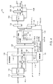
図4に示されるように、同期ポート(すなわち、ポートB)からの信号は、ラッチ104を用いて受信され得る。ラッチ104は、Bclkを受信するように構成されたクロック制御入力と、多重化回路102の第1の入力に連結される出力とを有し得る。同期クロックBclkは、制御回路101に供給され得る。制御回路101は、内部メモリクロック信号を生成するために使用され得、入ってくるメモリアクセス要求を遂行する順序を決定するように動作可能なシーケンス回路として機能し得る。特に、制御回路は、経路108を介して内部メモリクロックMclkを、経路124を介して同期化クロックArclkを、経路109を介してポートA出力クロックAoutclkを、経路111を介して出力制御クロックBoutclkを、および経路113を介して多重器制御信号PORTSELを生成するために使用され得る。
As shown in FIG. 4, a signal from the synchronization port (ie, port B) can be received using
非同期ポート(すなわち、ポートA)からの信号は、ラッチ112を用いて受信され得る。ラッチ112は、Aclkを受信するように構成されたクロック制御入力と、非同期ファーストインファーストアウト(FIFO)回路114に連結される出力とを有し得る。FIFO114は、ときには、バッファー回路と呼ばれ得る。非同期FIFO114は、ポートBからの要求が処理されている間に、ポートA上の入ってくる要求をバッファーするために使用され得る。FIFO114は、準安定性同期器(例えば、要求同期器116)に連結された出力を有し得る。特に、FIFO114は、現在の未処理の要求に関連付けられたデータおよびアドレス信号が提供される第1の出力と、信号Aasyncが提供される第2の出力とを有し得る。
A signal from the asynchronous port (ie, port A) can be received using
要求同期器116は、正エッジトリガー型ラッチ118と、負エッジトリガー型ラッチ120とを含み得る。正エッジトリガー型ラッチ118は、FIFO114の第2の出力から信号Aasyncを受信する入力と、経路124に連結された制御入力と、信号Areqが提供される出力とを有し得る。負エッジトリガー型ラッチ120は、FIFO114の第1の出力から現在未処理の要求に関連付けられたデータおよびアドレス信号を受信する第1の入力と、ラッチ118の出力から信号Areqを受信する第2の入力と、経路124に連結された制御入力と、多重器102の第2の入力に連結される第1の出力と、信号Areqsynが提供される第2の出力とを有し得る。信号Areqsynは、経路122を介して制御回路101に供給され得る。多重器102は、ポートAおよびBのうちの1つからのメモリアクセス要求信号をその出力へ選択的にルーティングさせるために、制御回路101から生成された信号PORTSELを用いて制御され得る。
メモリ行および列制御回路網(ときには、メモリアレイ制御回路網と呼ばれる)12は、多重器102の出力からデータおよびアドレシング信号を受信し得る。回路網12は、制御回路101から経路108を介して運搬された内部メモリクロックMclkを用いて制御され得る。回路網12はまた、現在サービスを提供されているメモリアクセス要求の完了を示すために、経路110を介して制御回路101に対して信号DONEを生成し得る。制御回路101を用いて生成された信号Arclkは、経路124を介してラッチ118および120の制御入力に供給され得る。FIFO114はまた、ラッチ118出力からフィードバックされる信号Areqと、信号Arclkを受信するように構成され得る。
Memory row and column control circuitry (sometimes referred to as memory array control circuitry) 12 may receive data and addressing signals from the output of
読み取り動作の間にメモリアレイ14から読み取られたデータ信号は、ポートB出力ラッチ130とポートA出力ラッチ132とに供給され得る。ポートA出力ラッチ132は、Aoutclkを用いて制御され得、その一方で、ポートB出力ラッチ130は、Boutclkを用いて制御され得る。信号AoutclkおよびBoutclkは、制御回路101を用いて生成され得る。ポートB出力ラッチ130は、ポートB出力信号Boutが提供される出力を有し得る。ポートA出力ラッチ132は、出力非同期FIFO134に連結された出力を有し得る。入力FIFO114に類似して、出力非同期FIFO134は、ポートA出力データ信号をバッファーするように機能し得る。次に、ポートA出力データ信号は、正エッジトリガー型ラッチ136および負エッジトリガー型ラッチ138を通過され得る。FIFO134、並びにラッチ136および138は、信号Aclkを用いてクロックされ得る。ラッチ138は、ポートA出力信号Aoutが提供される第1の出力と、ポートA出力確認信号Ackが提供される第2の出力とを有し得る。信号Ackは、経路140を介して非同期FIFO134にフィードバックされ得る。FIFO134において受信されるアサートされたAckは、データのワードが出力においてうまくラッチされたことを示し得、その内容をシフトするようにFIFO134を指示し得る。
Data signals read from
図5は、メモリアレイ14内に形成され得る例示的な単一ポートメモリセル100の回路ダイヤグラムである。図5に示されるように、セル100は、少なくとも1対の交差連結されたインバータ142および144を含み得、インバータ142および144は、各々、入力および出力を有する。インバータ142の入力は、インバータ144の出力に連結され得、その一方で、インバータ144の入力は、インバータ142の出力に連結され得る。インバータ144の出力は、セル100に対して第1の内部データストレージノードとして機能し得、その一方で、インバータ142の出力は、セル100に対して第2の内部データストレージノードとして機能し得る。この方法で交差連結されたインバータ142および144は、単一ビットのデータを格納するように機能し得(例えば、データビットの真バージョンが第1のデータストレージノード上に格納され得、その一方で、データビットの逆バージョンが第2のデータストレージノード上に格納され得る)、ときには、双安定要素と呼ばれ得る。
FIG. 5 is a circuit diagram of an exemplary single
第1のアクセストランジスタ146は、第1のデータストレージノードと第1のデータライン18−1との間に連結され得る。第2のアクセストランジスタ148は、第2のデータストレージノードと第2のデータライン18−2との間に連結され得る。データライン18−1および18−2は、ときには、真および補数ビットライン対と呼ばれ得る。データライン18−1および18−2は、書き込み動作の間にデータをセル100内に書き込むために適切な値に駆動され得、読み取り動作の間に電源電圧レベルに事前にチャージされ得る。
The
アクセストランジスタ146および148(ときには、アドレストランジスタと呼ばれる)は、ワードライン16を介して提供されるワードライン信号WLによって制御され得る。信号WLは、アクセスされるべきアレイ14内のメモリセル100のうちの1行を選択するようにアサートされ得る。残りの未選択の行の信号WLは、デアサートのままであり得る。図5の単一ポートメモリセルは、単なる例示に過ぎず、本発明の範囲を限定するものではない。必要に応じて、メモリセル100は、3つ以上の交差連結された反転回路を含み得、読み取りバッファー回路を含み得、単一端部構造等を有し得る。
図4に関連して説明されたTDMメモリ回路網の動作は、以下のようであり得る。一連のメモリアクセス要求は、同期ポートクロック(すなわち、ポートB)において立ち上りクロックエッジを検出することに応答してトリガーされ得る。内部メモリクロックMclkは、同期クロックBclkの立ち上りエッジでアサートするようにトリガーされ得、DONEの立ち上りエッジでネゲートする(すなわち、デアサートする)ようにトリガーされ得る。必要に応じて、Mclkは、DONEの立ち下りエッジでネゲートするようにトリガーされ得る。 The operation of the TDM memory circuitry described in connection with FIG. 4 may be as follows. A series of memory access requests can be triggered in response to detecting a rising clock edge in the synchronous port clock (ie, port B). The internal memory clock Mclk can be triggered to assert on the rising edge of the synchronous clock Bclk and can be triggered to negate (ie deassert) on the rising edge of DONE. If necessary, Mclk can be triggered to negate on the falling edge of DONE.
立ち上りMclkエッジを検出することに応答して、ポートBアクセスがすぐに実行されることにより、ポートBアクセス時間は、真デュアルポートメモリと同じぐらい速い(すなわち、デュアルポートメモリセルを用いて実装されたデュアルポートメモリが8個のメモリセルトランジスタを有する)。DONEがアサートされる場合に、Boutclkは、出力データ信号Boutをラッチするためにパルスの高レベルにされ得る。 In response to detecting the rising Mclk edge, port B access is performed immediately so that port B access time is as fast as a true dual port memory (ie, implemented using dual port memory cells). Dual port memory has 8 memory cell transistors). When DONE is asserted, Boutclk can be pulsed high to latch the output data signal Bout.
前述のように、ポートA入力非同期FIFO114は、入ってくるポートAメモリアクセス要求をバッファーするために使用され得る。信号Arclkは、ポートAメモリアクセス要求を同期させるために使用され得る。Mclkをトリガーすることに加えて、立ち上りBclkエッジは、所定の期間に対してパルスの高レベルにされているように信号Arclkをトリガーし得る。信号Aasyncは、概して、FIFO114が少なくとも1つの未処理のポートA要求を含む場合にアサートされ得る。ポートB要求が立ち上りBclkエッジの直後に処理されている間に、Aasyncは、ラッチ118を用いてAreqを生成するために、Arclkの第1の半サイクルの間にサンプリングされ(例えば、AasyncがArclkの正のクロックエッジでサンプリングされる)、その一方で、Areqは、ラッチ120を用いてAreqsynを生成するために、Arclkの第2の半サイクルの間にサンプリングされる(例えば、Areqsynが、Arclkの負のクロックエッジでサンプリングされる)。次に、同期されたポートA要求信号Areqsynは、ポートA要求が現在のBclkサイクルの間に依然遂行されていないことを示すために、制御回路101に供給され得る。この方法で未処理のポートA要求をサンプリングし、かつ再サンプリングすることは、ポートA要求を内部メモリクロックMclkに同期させるように機能し得る。
As described above, the port A input
信号AreqおよびArclkは、確認の形として非同期FIFO114にフィードバックされ得る。FIFO114が、Aclkにおいて負のエッジを検出し、かつ信号Areqがアサートされる場合に、Aasyncは、未処理の要求がサンプリングされたことを示す(例えば、FIFO114からその未処理の要求を削除する)ようにネゲートされ得る。その後に、非同期FIFO114は、その内容をシフトし得、FIFO114が、サービスを提供される必要がある追加の未処理の要求を含む場合に、Aasyncは、非同期的にアサートされる。
The signals Areq and Arclk can be fed back to the
図6は、同期ポートクロックが非同期ポートクロックより早い場合(例えば、Bclkが、Aclkの周波数より高い周波数を有する場合)の半同期TDMメモリ回路網の動作を例示するタイミングダイヤグラムである。図6の例は、非同期FIFO114が、時間t1の前に未処理の要求を含まないと仮定する。信号PORTSELは、処理のためにポートB要求を選択するデフォルトによって高であり得る。時間t1において、信号Aclkは、高をクロックし得、ポートA要求は、FIFO114に進入し得る。新しいポートA要求のこの追加は、t1のしばらく後に(例えば、時間t2において)、信号Aasyncが非同期的にアサートされるようにし得る。
FIG. 6 is a timing diagram illustrating the operation of the semi-synchronous TDM memory network when the synchronous port clock is earlier than the asynchronous port clock (eg, when Bclk has a higher frequency than the frequency of Aclk). The example of FIG. 6 assumes that
時間t3において、信号Bclkは、高をクロックし得、Bポート要求は、ラッチ104の出力において存在し得る(例えば、図4を参照)。Bclkのこの立ち上りエッジは、Mclkがアサートされるようにトリガーし得、ArclkがPWの所定のパルス幅に対してパルスの高レベルにされているようにトリガーし得る。Areqが、Aasyncと同じ値を有する(例えば、Aasyncが時間t3において高であるので、Arclkの立ち上りエッジは、Areqに高に立ち上らせる)ように、Arclkの立ち上りクロックエッジは、ラッチ118にAasyncをサンプリングさせ得る。
At time t3, signal Bclk can be clocked high, and a B port request can be present at the output of latch 104 (see, eg, FIG. 4). This rising edge of Bclk may be triggered so that Mclk is asserted, and Arclk may be triggered to be at a high level of the pulse for a predetermined pulse width of PW. The rising clock edge of Arclk is in
時間t4において、Arclkがデアサートされ得る。Arclkの立ち下りクロックエッジは、Aasyncにネゲートさせられ得(Areqが高である場合のみ)、Areqsynが、Areqと同じ値を有するように、ラッチ120にAreqをサンプリングさせ得る。この時間において、時間t1において到達したポートA要求が、要求同期器116によって既にラッチされたので、ポートA要求は、FIFO114から削除され得る。この例において、Areqが時間t4において高であるので、Arckの立ち下りエッジは、Areqsynに高に立ち上らせる。ポートAからの追加のメモリアクセス要求がないので、信号Aasyncは、ネゲートされたままであり得る。
At time t4, Arclk may be deasserted. The falling clock edge of Arclk can be negated by Aasync (only if Areq is high) and can cause
時間t5において、ポートBメモリアクセス要求が遂行され、信号DONEがパルスの高レベルにされ、それによってMclkがデアサートされ、Boutclkがパルスの高レベルにされるようにする。ポートBメモリアクセスの完了に応答して、信号Boutclkが、パルスの高レベルにされるのみであり得る。ポートBメモリアクセス要求の開始から対応する信号DONEがアサートされているまでの時間は、アクセス時間Tcoと等しい場合がある。(アサートされたAreqsynによって示されるように)未処理のポートAメモリ要求があるので、制御回路101は、ポートAメモリ要求がサービスを提供され得るように、一時的にPORTSELを反転し得る。
At time t5, a port B memory access request is fulfilled and signal DONE is pulsed high, thereby causing Mclk to be deasserted and Boutclk to be pulse high. In response to the completion of the port B memory access, the signal Boutclk may only be pulled high. The time from the start of the port B memory access request until the corresponding signal DONE is asserted may be equal to the access time Tco. Since there is an outstanding port A memory request (as indicated by asserted Areqsyn), the
時間t6において、DONEがデアサートされ得る。DONEが低である場合に、後のポートAメモリアクセスがサービスを提供され得る。未処理のポートAメモリ要求が存在するので、ポートAメモリアクセスの開始を表すために、Mclkが高に立ち上げられ得、Arclkがパルスの高レベルにされ得る。時間t6において、(低Aasyncによって示されるように)新しく到達するポートA要求がないので、Areqは、低に立ち下り得る。 At time t6, DONE can be deasserted. If DONE is low, a later port A memory access can be serviced. Since there is an outstanding port A memory request, Mclk can be raised high and Arclk can be pulsed high to indicate the start of port A memory access. At time t6, Areq can fall low because there are no newly arriving port A requests (as indicated by low Aasync).
時間t7において、Arclkがデアサートされ得る。Arclkの立ち下りクロックエッジがAreqをサンプリングし得、それによって、Areqが時間t7において低であるので、Areqsynに低に立ち下らせる。低Areqsynは、未処理のポートAメモリアクセス要求がないことを示し得る。時間t8において、信号DONEは、パルスの高レベルにされ、Mclkがデアサートされ、Aoutclkがパルスの高レベルにされるようにする。ポートAメモリアクセスの完了に応答して、信号Aoutclkが、パルスの高レベルにされるのみであり得る。この時間において、サービスを提供されるべきポートAまたはポートBからのさらなるメモリアクセス要求がない。時間t9において、Bclkは、高をクロックし得、第2のポートBメモリアクセス要求がサービスを提供され得る。時間t10において、Bclkは、高をクロックし得、第3のポートBメモリアクセス要求がサービスを提供され得る。 At time t7, Arclk may be deasserted. The falling clock edge of Arclk may sample Areq, thereby causing Areqsyn to fall low because Areq is low at time t7. A low Areqsyn may indicate that there are no outstanding port A memory access requests. At time t8, signal DONE is brought to the high level of the pulse, causing Mclk to be deasserted and Aoutclk to go to the high level of the pulse. In response to completion of the port A memory access, signal Aoutclk may only be pulled high. At this time, there are no further memory access requests from port A or port B to be serviced. At time t9, Bclk may clock high and a second port B memory access request may be serviced. At time t10, Bclk may clock high and a third port B memory access request may be serviced.
BclkがAclkより早いこのシナリオにおいて、ポートAアクセスの待ち時間は、多くても1つのポートBサイクル分のみ増加され、これは、真デュアルポートエミュレーションにおいて許容可能であり得る。BclkがAclkよりさらに早い場合(例えば、Bclkが、Aclkより少なくとも3倍、少なくとも5倍、または少なくとも10倍早い場合)、ポートAアクセスは、Aclkの小数の範囲内に完了されると保証され得る。 In this scenario where Bclk is faster than Aclk, the latency of port A access is increased by at most one port B cycle, which may be acceptable in true dual port emulation. If Bclk is even earlier than Aclk (eg, if Bclk is at least 3 times, at least 5 times, or at least 10 times earlier than Aclk), port A access may be guaranteed to be completed within a fraction of Aclk. .
図7は、非同期ポートクロックが同期ポートクロックより早い場合(例えば、Bclkは、Aclkの周波数より低い周波数を有する場合)、半同期TDMメモリ回路網の動作を例示するタイミングダイヤグラムである。図7の例は、非同期FIFO114が、(時間t1の前にアサートされたAasyncによって示されるように)時間t1の前に少なくとも1つの未処理の要求を含むと仮定する。信号PORTSELは、処理のためにポートB要求を選択するデフォルトによって高であり得る。
FIG. 7 is a timing diagram illustrating the operation of the semi-synchronous TDM memory circuitry when the asynchronous port clock is earlier than the synchronous port clock (eg, Bclk has a frequency lower than the frequency of Aclk). The example of FIG. 7 assumes that the
時間t1において、信号AclkおよびBclkは、同時に高をクロックし得る(例えば、新しいポートAメモリアクセス要求および新しいポートBメモリアクセス要求は、並列に到達し得る)。(Aasyncが時間t1において高であるので)立ち上りBclkは、ArclkおよびMclkが高をクロックし、Areqが立ち上るようにトリガーする。同期ポートアクセス(すなわち、ポートBメモリアクセス)は、すぐに開始され得る。時間t2において、Arclkは、低をクロックし得、Aasyncにネゲートさせ(例えば、時間t1の前にFIFO114内に格納された未処理のメモリアクセス要求が既に要求同調器116によってラッチされたので、未処理のメモリアクセス要求がFIFO114から削除され得る)、(Areqが時間t2において高であるので)Areqsynに高に立ち上らせる。時間t3において、信号DONEは、ポートBメモリアクセスの完了を示すために一時的にアサートされ得、それによってMclkが低をクロックするようにトリガーする。この時間において、高Areqsynによって示されるように、サービスを提供される必要がある少なくとも1つの未処理のポートA要求(すなわち、現在に同調器116内に格納されているサービスを提供されていないポートA要求)があるので、PORTSELは、サービスを提供するために、ポートAを選択するように低に駆動され得る。時間t3の直後、FIFO114が、依然、時間t1において到達した待機のポートBメモリアクセスを含むので、信号Aasyncがアサートされ得る。
At time t1, signals Aclk and Bclk may clock high simultaneously (eg, a new port A memory access request and a new port B memory access request may arrive in parallel). Rising Bclk triggers Arclk and Mclk to clock high and Areq to rise (since Aasync is high at time t1). Synchronous port access (ie, port B memory access) can be initiated immediately. At time t2, Arclk may clock low and negate Async (e.g., since the outstanding memory access request stored in
時間t4において、DONEは、デアサートされ得、時間t1の前にFIFO114内に格納された未処理のポートBメモリアクセスがサービスを提供され得る。この時間において、制御回路101は、ArclkおよびMclkを高に駆動し得る。信号Aasyncがラッチ118の間にサンプリングされ得るが、Aasyncが時間t4において高であるので、Areqは、高のままであり得る。時間t5において、Arclkは、低をクロックし得、Aasyncにネゲートさせる(例えば、時間t1において到達した未処理のメモリアクセス要求が要求同調器116によってラッチされたので、未処理のメモリアクセス要求が削除され得る)。信号Areqは、ラッチ120を用いてサンプリングされ得るが、Areqが時間t5において高であるので、Areqsynは高のままである。時間t6において、信号DONEは、待機のポートAメモリアクセスの完了を示すために一時的にアサートされ得、それによってMclkが低をクロックするようにトリガーする。依然サービスを提供されるポートAメモリアクセス要求があるので、信号PORTSELは低のままであり得る。時間t6の周辺において、Aclkは、高をクロックし得、第1の追加のポートAメモリアクセス要求は、FIFO114に進入し得る。時間t6の直後に、FIFO114が、依然、時間t6において到達した第1の追加のポートAメモリアクセスを含むので、信号Aasyncがアサートされ得る。
At time t4, DONE can be deasserted and outstanding port B memory accesses stored in
時間t7において、DONEがデアサートされ得、時間t1において到達した(かつ現在同期器116内に格納されている)未処理のポートAメモリアクセスがサービスを提供され得る。この時間において、制御回路101は、ArclkおよびMclkを高に駆動し得る。信号Aasyncは、ラッチ118を用いてサンプリングされ得、Aasyncが時間t7において高であるので、Areqは高のままである。時間t8において、Arclkは、低をクロックし得、Aasyncにネゲートさせる(例えば、時間t6において到達した第1の追加のポートAメモリアクセス要求が削除され得る。信号Areqは、ラッチ220を用いてサンプリングされ得、Areqが時間t8において高であるので、Areqsynは高のままである。時間t9において、信号DONEは、現在のポートAメモリアクセスの完了を示すために一時的にアサートされ得、それによってMclkが低をクロックするようにトリガーする。依然サービスを提供される第1の追加のポートAメモリアクセス要求があるので、信号PORTSELは低のままであり得る。この時間においてFIFO114内に追加の待機の要求がないので、信号Aasyncは、ネゲートされたままであり得る。
At time t7, DONE can be deasserted and the outstanding port A memory access that arrived at time t1 (and is currently stored in the synchronizer 116) can be served. At this time, the
時間t10において、DONEがデアサートされ得、時間t6において第1の追加のポートAメモリアクセス要求がサービスを提供され得る。この時間において、制御回路101は、ArclkおよびMclkを高に駆動し得る。信号Aasyncは、ラッチ118を用いてサンプリングされ得、Aasyncが時間t10において低であるので、Areqに低に立ち下らせる。時間t11において、Aclkは、高をクロックし得、第2の追加のポートAメモリアクセス要求は、FIFO114に進入し得、Aasyncに高に立ち上らせる。時間t12において、Arclkは低をクロックし得る。Areqが低であるので、FIFO114から削除される必要がある要求がない(例えば、FIFO114は、Areqが高である場合およびその場合のみ、Arclkの立ち下りクロックエッジにおいて要求を削除するように構成されるのみであり得る)。信号Areqは、ラッチ120を用いてサンプリングされ得、Areqが時間t12において高であるので、Areqsynに低に立ち下らせる。時間t13において、信号DONEは、第1の追加のポートAメモリアクセスの完了を示すために一時的にアサートされ得、それによって、Mclkが低をクロックするようにトリガーする。Areqが低である場合、信号PORTSELは、高に戻るように駆動され得る。現在のBclkサイクルの残りに対してサービスを提供される追加のポートA要求がないので、信号Aasyncは、高のままである。時間t14において、新しいポートAメモリ要求は、少なくともBclkの立ち上りエッジまで到達し、そしてFIFO114内に格納され得る。
At time t10, DONE can be deasserted and at time t6 a first additional port A memory access request can be serviced. At this time, the
AclkがBclkより早いこのシナリオにおいて、FIFO114の深さは、ポートBクロックサイクルにおいて発生し得るポートA要求の数を収容するのに十分に深いように構成され得る。必要に応じて、図1に関連して説明された非同期仲裁多重ポートエミュレーションアプローチは、AclkがBclkより早い場合に使用され得る。
In this scenario where Aclk is faster than Bclk, the depth of the
図8は、図4において示されるタイプの半同期TDM多重ポートメモリ回路網を用いてメモリアクセス要求を遂行することに伴う例示的なステップのフローチャートである。ステップ300において、制御回路101は、Bclk立ち上りエッジを待ち得る。信号PORTSELは、そのデフォルト値(1)に(すなわち、同期ポートB要求をメモリアレイ制御回路網12に選択的にルーティングさせるように)設定され得る。入力FIFO114が空ではない場合、信号Aasyncは、1に非同期的に設定され得る(ステップ302)。
FIG. 8 is a flowchart of exemplary steps involved in performing a memory access request using a semi-synchronous TDM multi-port memory network of the type shown in FIG. In
立ち上りBclkエッジを検出することに応答して、制御回路101は、内部メモリクロックMclkを立ち上らせ、Arclkをパルスの高レベルにし得る(ステップ304)。ステップ306において、Aasyncは、ラッチ118を用いてサンプリングされ得る(例えば、AreqがAasyncのサンプリングされた値に設定される)。サービスを提供されるポートBメモリアクセスがある場合に、処理は、ステップ310に進み得る。ポートB要求が存在しない場合に、Arclkがネゲートされた後に、処理は、ステップ318に進み得る。
In response to detecting the rising Bclk edge, the
ステップ310において、所望のポートB読み取り/書き込みメモリアクセスが実行され得る。ステップ312に示されるように、立ち下りArclkエッジを検出することに応答して、Areqは、ラッチ120を用いてサンプリングされ得る(例えば、Areqsynは、Areqのサンプリングされた値に設定される)。Areqが高である場合に、FIFO114の出力がラッチされ、それによって、Aasyncにネゲートさせられ、最も古いポートAメモリアクセス要求(すなわち、現在FIFO内に格納された任意の他の要求の前に到達したポートAメモリアクセス要求)は、FIFO114から削除され得る。ステップ314において、DONEは、パルスの高レベルにされ得、それによってMclkが低をクロックし、Boutclkがパルスの高レベルにするようにトリガーする。
In
ステップ316において、FIFO114が少なくとも1つのサービスを提供されていない要求を含む場合に、Aasyncがアサートされ得る。経路317によって示されるように、次に、処理は、ステップ318へ進み得る。ステップ318において、制御回路101は、Areqsynが高であるか低であるかをチェックし得る。Areqsynが低である場合、処理は、経路320によって示されるように、ステップ300に戻るようにループし得る(例えば、制御回路101は、現在のBclkサイクルの残りに対して任意のポートA要求を遅延させ得る。Areqsynが高である場合、処理は、ステップ320へ進み得る。
In
ステップ320において、信号PORTSELが、0に(すなわち、非同期ポートA要求をメモリアレイ制御回路網12に選択的にルーティングさせるように)設定され得る。信号DONEが低に立ち下ることを検出することに応答して、信号Mclkが高をクロックされ得、Arclkがパルスの高レベルにされ得る(ステップ322)。ステップ324において、Aasyncは、ラッチ118を用いてサンプリングされ得る(例えば、Areqが、Aasyncのサンプリングされた値に設定される)。ステップ326において、所望のポートA読み取り/書き込みメモリアクセスが実行され得る。ステップ328において示されるように、立ち下りArclkエッジの検出に応答して、Areqは、ラッチ120を用いてサンプリングされ得る(例えば、AreqsynがAreqのサンプリングされた値に設定される)。Areqが高である場合、Aasyncがネゲートされ得る(例えば、現在FIFO114内に格納された最も古いポートAメモリアクセス要求が除去され得る)。ステップ330において、DONEがパルスの高レベルにされ得、それによって、Mclkが低をクロックし、かつAoutclkがパルスの高レベルにするようにトリガーする。経路332によって示されるように、(存在するなら)処理は追加のAポート要求を処理するために、ステップ316に戻るようにループし得る。
In
図1の仲裁回路22を有するメモリ回路網と、図4の半同期TDMシーケンス回路101を有するメモリ回路網とのデュアルポート実装は、単なる例示に過ぎず、本発明の範囲を限定するように機能しない。必要に応じて、本明細書において説明された非同期および半同期デュアルポートエミュレーション技術は、3ポートメモリ動作、4ポートメモリ動作等をエミュレートするために適用され得る。
The dual port implementation of the memory circuitry having the
追加の実施形態:
追加の実施形態1:第1のポートと第2のポートとを有するデュアルポートメモリを動作させる方法であって、該デュアルポートメモリは、単一ポートメモリ要素のアレイを含み、該方法は、該第1のポートにおいて、第1のメモリアクセス要求と、関連付けられた第1のクロック信号とを受信することと、該第2のポートにおいて、第2のメモリアクセス要求と、関連付けられた第2のクロック信号とを受信することと、制御回路を用いて該第2のクロック信号の立ち上りクロックエッジを検出することに応答して、第3のクロック信号を生成し、かつ該第2のメモリアクセス要求にサービスを提供することと、該第2のメモリアクセス要求がサービスを提供されている間に、該第3のクロック信号を用いて該第1のメモリアクセス要求をサンプリングすることとを含む、方法。
Additional embodiments:
Additional embodiment 1: A method of operating a dual port memory having a first port and a second port, the dual port memory comprising an array of single port memory elements, the method comprising: Receiving a first memory access request and an associated first clock signal at the first port; and a second memory access request associated with the second memory access request at the second port. In response to receiving the clock signal and detecting a rising clock edge of the second clock signal using the control circuit, and generating a third clock signal and the second memory access request And providing the first memory access request using the third clock signal while the second memory access request is being serviced. And a to sampling method.
追加の実施形態2:上記第3のクロック信号を用いて上記第1のメモリアクセス要求をサンプリングすることは、少なくとも2つの直列接続されたラッチを用いて該第3のクロック信号の立ち上りおよび立ち下りクロックエッジの時に該第1のメモリアクセス要求をサンプリングすることを含む、追加の実施形態1の方法。
Additional embodiment 2: Sampling of the first memory access request using the third clock signal is performed by using at least two serially connected latches to rise and fall of the third clock signal. The method of
追加の実施形態3:上記第1のメモリアクセス要求をバッファー回路内に格納することをさらに含み、該バッファー回路は、上記少なくとも2つの直列接続されたラッチから制御信号を受信するように動作可能である、追加の実施形態2の方法。 Additional embodiment 3: further comprising storing the first memory access request in a buffer circuit, the buffer circuit being operable to receive a control signal from the at least two serially connected latches. An additional embodiment 2 method.
追加の実施形態4:上記バッファー回路を用いて上記第3のクロック信号を受信することをさらに含む、追加の実施形態3の方法。 Additional embodiment 4: The method of additional embodiment 3, further comprising receiving the third clock signal using the buffer circuit.
追加の実施形態5:上記デュアルポートメモリは、多重化回路を含み、該多重化回路は、上記少なくとも2つの直列接続されたラッチを介して上記第1のメモリアクセス要求を受信するように動作可能な第1の入力と、上記第2のメモリアクセス要求を受信するように動作可能な第2の入力と、上記制御回路から制御信号を受信するように動作可能な制御入力とを有する、追加の実施形態2の方法。 Additional embodiment 5: The dual port memory includes a multiplexing circuit, the multiplexing circuit operable to receive the first memory access request via the at least two serially connected latches. An additional first input, a second input operable to receive the second memory access request, and a control input operable to receive a control signal from the control circuit. Embodiment 2. The method of embodiment 2.
追加の実施形態6:上記第1のメモリアクセス要求をバッファー回路内に格納することをさらに含む、追加の実施形態1の方法。
Additional embodiment 6: The method of
追加の実施形態7:上記制御回路を用いて上記第2のクロック信号の上記立ち上りクロックエッジを検出することに応答して、上記単一ポートメモリ要素のアレイへのアクセスを制御するための第4のクロック信号を生成することをさらに含む、追加の実施形態1の方法。
Additional embodiment 7: A fourth for controlling access to the array of single port memory elements in response to detecting the rising clock edge of the second clock signal using the control circuit. The method of
追加の実施形態8:上記第2のメモリアクセス要求が遂行されることに応答して、上記制御回路を用いて該第2のメモリアクセス要求の完了を表す制御信号を受信することと、該制御回路を用いて該制御信号を受信することに応答して、上記第1のメモリアクセス要求にサービスを提供することとをさらに含む、追加の実施形態1の方法。
Additional embodiment 8: In response to the execution of the second memory access request, receiving a control signal indicating completion of the second memory access request using the control circuit; and The method of
追加の実施形態9:第1のポートと第2のポートとを有するデュアルポートメモリを動作させる方法であって、該デュアルポートメモリは、単一ポートメモリ要素のアレイを含み、該方法は、該第1のポートにおいて、第1のメモリアクセス要求と、関連付けられた第1のクロック信号とを受信することと、該第2のポートにおいて、第2のメモリアクセス要求と、関連付けられた第2のクロック信号とを受信することと、該第1のクロック信号のクロックが上昇することに応答して、該第1のメモリアクセス要求をバッファー内に一時的に格納することと、制御回路を用いて該第2のクロック信号の立ち上りクロックエッジを検出することに応答して、該第1のメモリアクセス要求が該バッファー内に格納されている間に、該第2のメモリアクセス要求にサービスを提供することとを含む、方法。 Additional embodiment 9: A method of operating a dual port memory having a first port and a second port, the dual port memory comprising an array of single port memory elements, the method comprising: Receiving a first memory access request and an associated first clock signal at the first port; and a second memory access request associated with the second memory access request at the second port. Receiving the clock signal, temporarily storing the first memory access request in a buffer in response to the rising of the clock of the first clock signal, and using a control circuit In response to detecting a rising clock edge of the second clock signal, the second memory while the first memory access request is stored in the buffer. And providing a service to the access request, the method.
追加の実施形態10:上記第2のクロック信号の上記立ち上りクロックエッジを検出することに応答して、上記制御回路を用いて第3のクロック信号をトリガーすることをさらに含む、追加の実施形態9の方法。 Additional embodiment 10: Additional embodiment 9 further comprising triggering a third clock signal using the control circuit in response to detecting the rising clock edge of the second clock signal. the method of.
追加の実施形態11:同期化回路を用いて上記第3のクロック信号を受信することであって、該同期化回路は、少なくとも2つのラッチを含む、ことと、上記バッファーを用いて該第3のクロック信号を受信することとをさらに含む、追加の実施形態10の方法。
Additional embodiment 11: Receiving the third clock signal using a synchronization circuit, wherein the synchronization circuit includes at least two latches, and using the buffer, the third clock signal 11. The method of
追加の実施形態12:上記少なくとも2つのラッチは、上記第3のクロック信号の立ち上りクロックエッジの時にデータをラッチするように構成された正エッジトリガー型ラッチと、該第3のクロック信号の立ち下りクロックエッジの時にデータをラッチするように構成された負エッジトリガー型ラッチと含む、追加の実施形態11の方法。 Additional embodiment 12: The at least two latches include a positive edge triggered latch configured to latch data at a rising clock edge of the third clock signal, and a falling edge of the third clock signal. 12. The method of additional embodiment 11, comprising a negative edge triggered latch configured to latch data on a clock edge.
追加の実施形態13:上記バッファーを用いて上記同期化回路から制御信号を受信することをさらに含む、追加の実施形態11の方法。 Additional embodiment 13: The method of additional embodiment 11, further comprising receiving a control signal from the synchronization circuit using the buffer.
追加の実施形態14:上記同期化回路を用いて上記第1のメモリアクセス要求をラッチすることと、該第1のメモリアクセス要求が該同期化回路を用いてラッチされた後に、該第1のメモリアクセス要求を上記バッファーから除去することとをさらに含む、追加の実施形態11の方法。
Additional embodiment 14: latching the first memory access request using the synchronization circuit; and after the first memory access request is latched using the synchronization circuit, the first
追加の実施形態15:上記バッファーは、ファーストインファーストアウト回路を含む、追加の実施形態9の方法。 Additional embodiment 15: The method of additional embodiment 9, wherein the buffer includes a first-in first-out circuit.
追加の実施形態16:第1のポートと第2のポートとを有するデュアルポートメモリであって、該デュアルポートメモリは、単一ポートメモリ要素のアレイと、第1のメモリアクセス要求と、該第1のポートに関連付けられた第1のクロック信号とを受信するように動作可能な第1の入力ラッチと、第2のメモリアクセス要求と、該第2のポートに関連付けられた第2のクロック信号とを受信するように動作可能な第2の入力ラッチであって、該第2のクロック信号は、該第1のクロック信号と異なる、第2の入力ラッチと、該第1のクロック信号を受信せず、該第2のクロック信号を受信するように動作可能な制御回路とを含み、該制御回路は、該第1のメモリアクセス要求および該第2のメモリアクセス要求のうちのいずれが遂行のために選択されるべきであるかを決定する制御信号を生成するようにさらに動作可能である、デュアルポートメモリ。 Additional embodiment 16: A dual port memory having a first port and a second port, the dual port memory comprising an array of single port memory elements, a first memory access request, and the second A first input latch operable to receive a first clock signal associated with a port; a second memory access request; and a second clock signal associated with the second port. A second input latch operable to receive the second input latch, wherein the second clock signal is different from the first clock signal and receives the first clock signal. And a control circuit operable to receive the second clock signal, wherein the control circuit performs any one of the first memory access request and the second memory access request. For It is further operable to generate a control signal which determines whether it should be selected, the dual port memory.
追加の実施形態17:上記第1の入力ラッチから上記第1のメモリアクセス要求を受信するように動作可能な第1の入力と、上記第2の入力ラッチから上記第2のメモリアクセス要求を受信するように動作可能な第2の入力と、上記制御回路から上記制御信号を受信するように動作可能な制御入力とを有する多重化回路をさらに含む、追加の実施形態16の方法。
Additional embodiment 17: receiving a first input operable to receive the first memory access request from the first input latch and the second memory access request from the second input latch The method of
追加の実施形態18:上記第1の入力ラッチと上記多重化回路の上記第1の入力との間に連結されたバッファーをさらに含む、追加の実施形態17の方法。
Additional embodiment 18: The method of
追加の実施形態19:上記バッファーと上記多重化回路の上記第1の入力との間に連結された正エッジトリガー型ラッチおよび負エッジトリガー型ラッチをさらに含む、追加の実施形態18の方法。
Additional embodiment 19: The method of
追加の実施形態20:上記バッファーは、ファーストインファーストアウト回路を含む、追加の実施形態18の方法。
Additional embodiment 20: The method of
上記の内容は、単なる本発明の原理の例示に過ぎず、さまざまな改変が、本発明の範囲および精神から逸脱することなしに、当業者によって加えられ得る。上記実施形態は、単独も任意の組み合わせでも実装され得る。 The foregoing is merely illustrative of the principles of this invention and various modifications can be made by those skilled in the art without departing from the scope and spirit of the invention. The above embodiments can be implemented alone or in any combination.
Claims (19)
該第1のポートにおいて、第1のメモリアクセス要求と、関連付けられた第1のクロック信号とを受信することと、
該第2のポートにおいて、第2のメモリアクセス要求と、関連付けられた第2のクロック信号とを受信することと、
制御回路を用いて該第2のクロック信号の立ち上りクロックエッジを検出することに応答して、第3のクロック信号を生成し、かつ該第2のメモリアクセス要求にサービスを提供することと、
該第2のメモリアクセス要求がサービスを提供されている間に、該第3のクロック信号を用いて該第1のメモリアクセス要求をサンプリングすることと
を含む、方法。 A method of operating a dual port memory having a first port and a second port, the dual port memory comprising an array of single port memory elements, the method comprising:
Receiving, at the first port, a first memory access request and an associated first clock signal;
Receiving a second memory access request and an associated second clock signal at the second port;
In response to detecting a rising clock edge of the second clock signal using a control circuit, generating a third clock signal and servicing the second memory access request;
Sampling the first memory access request using the third clock signal while the second memory access request is being serviced.
該制御回路を用いて該制御信号を受信することに応答して、前記第1のメモリアクセス要求にサービスを提供することと
をさらに含む、請求項1に記載の方法。 Responsive to the execution of the second memory access request, receiving a control signal representing completion of the second memory access request using the control circuit;
The method of claim 1, further comprising: servicing the first memory access request in response to receiving the control signal using the control circuit.
該第1のポートにおいて、第1のメモリアクセス要求と、関連付けられた第1のクロック信号とを受信することと、
該第2のポートにおいて、第2のメモリアクセス要求と、関連付けられた第2のクロック信号とを受信することと、
該第1のクロック信号が上昇することに応答して、該第1のメモリアクセス要求をバッファー内に一時的に格納することと、
制御回路を用いて該第2のクロック信号の立ち上りクロックエッジを検出することに応答して、該第1のメモリアクセス要求が該バッファー内に格納されている間に、該第2のメモリアクセス要求にサービスを提供することと
を含む、方法。 A method of operating a dual port memory having a first port and a second port, the dual port memory comprising an array of single port memory elements, the method comprising:
Receiving, at the first port, a first memory access request and an associated first clock signal;
Receiving a second memory access request and an associated second clock signal at the second port;
In response to the first clock signal rising, temporarily storing the first memory access request in a buffer;
In response to detecting a rising clock edge of the second clock signal using a control circuit, while the first memory access request is stored in the buffer, the second memory access request Providing a service.
前記バッファーを用いて該第3のクロック信号を受信することと
をさらに含む、請求項10に記載の方法。 Receiving the third clock signal using a synchronization circuit, the synchronization circuit including at least two latches;
The method of claim 10, further comprising: receiving the third clock signal using the buffer.
該第1のメモリアクセス要求が該同期化回路を用いてラッチされた後に、該第1のメモリアクセス要求を前記バッファーから除去することと
をさらに含む、請求項11に記載の方法。 Latching the first memory access request using the synchronization circuit;
The method of claim 11, further comprising: removing the first memory access request from the buffer after the first memory access request is latched using the synchronization circuit.
単一ポートメモリ要素のアレイと、
第1のメモリアクセス要求と、該第1のポートに関連付けられた第1のクロック信号とを受信するように動作可能な第1の入力ラッチと、
第2のメモリアクセス要求と、該第2のポートに関連付けられた第2のクロック信号とを受信するように動作可能な第2の入力ラッチであって、該第2のクロック信号は、該第1のクロック信号と異なる、第2の入力ラッチと、
該第1のクロック信号を受信するように動作可能ではなく、かつ該第2のクロック信号を受信するように動作可能な制御回路であって、該制御回路は、該第1のメモリアクセス要求および該第2のメモリアクセス要求のうちのいずれが遂行のために選択されるべきであるかを決定する制御信号を生成するようにさらに動作可能である、制御回路と、
該第1の入力ラッチから該第1のメモリアクセス要求を受信するように動作可能な第1の入力と、該第2の入力ラッチから該第2のメモリアクセス要求を受信するように動作可能な第2の入力と、該制御回路から該制御信号を受信するように動作可能な制御入力とを有する多重化回路と
を含む、デュアルポートメモリ。 A dual port memory having a first port and a second port, the dual port memory comprising:
An array of single-port memory elements;
A first input latch operable to receive a first memory access request and a first clock signal associated with the first port;
A second input latch operable to receive a second memory access request and a second clock signal associated with the second port, wherein the second clock signal is the second clock signal; A second input latch different from the clock signal of 1;
A control circuit not operable to receive the first clock signal and operable to receive the second clock signal, the control circuit including the first memory access request and A control circuit, further operable to generate a control signal that determines which of the second memory access requests should be selected for performance;
A first input operable to receive the first memory access request from the first input latch and operable to receive the second memory access request from the second input latch A dual port memory comprising: a multiplexing circuit having a second input and a control input operable to receive the control signal from the control circuit.
Applications Claiming Priority (2)
| Application Number | Priority Date | Filing Date | Title |
|---|---|---|---|
| US13/284,721 | 2011-10-28 | ||
| US13/284,721 US8806259B2 (en) | 2011-10-28 | 2011-10-28 | Time division multiplexed multiport memory implemented using single-port memory elements |
Related Child Applications (1)
| Application Number | Title | Priority Date | Filing Date |
|---|---|---|---|
| JP2017018597A Division JP6293322B2 (en) | 2011-10-28 | 2017-02-03 | Time division multiplexed multiport memory. |
Publications (3)
| Publication Number | Publication Date |
|---|---|
| JP2013097792A JP2013097792A (en) | 2013-05-20 |
| JP2013097792A5 JP2013097792A5 (en) | 2015-09-24 |
| JP6088200B2 true JP6088200B2 (en) | 2017-03-01 |
Family
ID=47225945
Family Applications (2)
| Application Number | Title | Priority Date | Filing Date |
|---|---|---|---|
| JP2012232813A Expired - Fee Related JP6088200B2 (en) | 2011-10-28 | 2012-10-22 | Time division multiplexed multiport memory. |
| JP2017018597A Active JP6293322B2 (en) | 2011-10-28 | 2017-02-03 | Time division multiplexed multiport memory. |
Family Applications After (1)
| Application Number | Title | Priority Date | Filing Date |
|---|---|---|---|
| JP2017018597A Active JP6293322B2 (en) | 2011-10-28 | 2017-02-03 | Time division multiplexed multiport memory. |
Country Status (4)
| Country | Link |
|---|---|
| US (2) | US8806259B2 (en) |
| EP (1) | EP2587486B1 (en) |
| JP (2) | JP6088200B2 (en) |
| CN (1) | CN103093808B (en) |
Families Citing this family (9)
| Publication number | Priority date | Publication date | Assignee | Title |
|---|---|---|---|---|
| US9230622B2 (en) * | 2012-11-30 | 2016-01-05 | Taiwan Semiconductor Manufacturing Company, Ltd. | Simultaneous two/dual port access on 6T SRAM |
| US10289186B1 (en) * | 2013-10-31 | 2019-05-14 | Maxim Integrated Products, Inc. | Systems and methods to improve energy efficiency using adaptive mode switching |
| CN104318952B (en) * | 2014-09-30 | 2017-11-10 | 西安紫光国芯半导体有限公司 | A kind of circuit and method for reducing voltage port in DRAM |
| US10430215B1 (en) * | 2015-06-25 | 2019-10-01 | Cadence Design Systems, Inc. | Method and system to transfer data between hardware emulator and host workstation |
| JP6637872B2 (en) * | 2016-10-28 | 2020-01-29 | ルネサスエレクトロニクス株式会社 | Multiport memory and semiconductor device |
| US10652912B2 (en) | 2018-04-30 | 2020-05-12 | Microchip Technology Incorporated | Smart radio arbiter with conflict resolution based on timing predictability |
| US11194942B1 (en) * | 2018-12-06 | 2021-12-07 | Cadence Design Systems, Inc. | Emulation system supporting four-state for sequential logic circuits |
| CN110059036B (en) * | 2019-04-15 | 2022-04-26 | 西安微电子技术研究所 | Access control device and method for multiple asynchronous interfaces in memory bank |
| KR20210104498A (en) * | 2020-02-17 | 2021-08-25 | 에스케이하이닉스 주식회사 | Semiconductor device |
Family Cites Families (25)
| Publication number | Priority date | Publication date | Assignee | Title |
|---|---|---|---|---|
| JPS63285648A (en) * | 1987-05-19 | 1988-11-22 | Fujitsu Ltd | System for arbitrating memory access |
| US4796232A (en) | 1987-10-20 | 1989-01-03 | Contel Corporation | Dual port memory controller |
| US4937781A (en) | 1988-05-13 | 1990-06-26 | Dallas Semiconductor Corporation | Dual port ram with arbitration status register |
| US5047921A (en) | 1989-01-31 | 1991-09-10 | International Business Machines Corporation | Asynchronous microprocessor random access memory arbitration controller |
| US5708850A (en) * | 1994-07-27 | 1998-01-13 | Sony Corporation | Parallel processing system for time division multiplex data transfer including read/write dual port memory accessible to bus and digital signal processor during opposite phases of clock |
| JPH0944395A (en) * | 1995-08-02 | 1997-02-14 | Fujitsu Ltd | Asynchronous access arbitration system |
| US5768211A (en) | 1996-07-31 | 1998-06-16 | Cypress Semiconductor Corporation | Multi-port arbitration for high performance width expansion |
| TW451215B (en) * | 1998-06-23 | 2001-08-21 | Motorola Inc | Pipelined dual port integrated circuit memory |
| US5973985A (en) | 1998-08-11 | 1999-10-26 | Stmicroelectronics, Inc. | Dual port SRAM cell having pseudo ground line or pseudo power line |
| US6388939B1 (en) | 1999-09-30 | 2002-05-14 | Cypress Semiconductor Corp. | Dual port sram |
| US6118689A (en) | 1999-10-27 | 2000-09-12 | Kuo; James B. | Two-port 6T CMOS SRAM cell structure for low-voltage VLSI SRAM with single-bit-line simultaneous read-and-write access (SBLSRWA) capability |
| US6816955B1 (en) | 2000-09-29 | 2004-11-09 | Cypress Semiconductor Corp. | Logic for providing arbitration for synchronous dual-port memory |
| US6751151B2 (en) | 2001-04-05 | 2004-06-15 | International Business Machines Corporation | Ultra high-speed DDP-SRAM cache |
| US6606275B2 (en) | 2001-08-23 | 2003-08-12 | Jeng-Jye Shau | High performance semiconductor memory devices |
| US7421559B1 (en) * | 2003-12-18 | 2008-09-02 | Cypress Semiconductor Corporation | Apparatus and method for a synchronous multi-port memory |
| KR100560948B1 (en) | 2004-03-31 | 2006-03-14 | 매그나칩 반도체 유한회사 | 6 Transistor Dual Port SRAM Cell |
| JP2006252656A (en) | 2005-03-10 | 2006-09-21 | Nec Electronics Corp | Multi-port memory device |
| JP4914034B2 (en) | 2005-06-28 | 2012-04-11 | セイコーエプソン株式会社 | Semiconductor integrated circuit |
| JP4425243B2 (en) * | 2005-10-17 | 2010-03-03 | Okiセミコンダクタ株式会社 | Semiconductor memory device |
| US7603496B2 (en) * | 2006-01-23 | 2009-10-13 | Arm Limited | Buffering data during data transfer through a plurality of channels |
| JP5038657B2 (en) * | 2006-06-26 | 2012-10-03 | ルネサスエレクトロニクス株式会社 | Semiconductor integrated circuit device |
| US7564738B2 (en) | 2006-08-11 | 2009-07-21 | Freescale Semiconductor, Inc. | Double-rate memory |
| KR100846386B1 (en) * | 2006-09-21 | 2008-07-15 | 주식회사 하이닉스반도체 | Multi port memory device |
| JP2009238351A (en) * | 2008-03-28 | 2009-10-15 | Oki Semiconductor Co Ltd | Dual-port semiconductor storage device and its timing generating device |
| JP2010044821A (en) * | 2008-08-11 | 2010-02-25 | Hitachi Ulsi Systems Co Ltd | Semiconductor device and memory macro |
-
2011
- 2011-10-28 US US13/284,721 patent/US8806259B2/en active Active
-
2012
- 2012-10-22 EP EP12189371.3A patent/EP2587486B1/en active Active
- 2012-10-22 JP JP2012232813A patent/JP6088200B2/en not_active Expired - Fee Related
- 2012-10-29 CN CN201210421421.2A patent/CN103093808B/en active Active
-
2014
- 2014-07-15 US US14/332,006 patent/US9298211B2/en active Active
-
2017
- 2017-02-03 JP JP2017018597A patent/JP6293322B2/en active Active
Also Published As
| Publication number | Publication date |
|---|---|
| US9298211B2 (en) | 2016-03-29 |
| EP2587486A2 (en) | 2013-05-01 |
| JP2013097792A (en) | 2013-05-20 |
| EP2587486B1 (en) | 2019-09-11 |
| JP6293322B2 (en) | 2018-03-14 |
| US8806259B2 (en) | 2014-08-12 |
| EP2587486A3 (en) | 2013-06-12 |
| US20140331074A1 (en) | 2014-11-06 |
| US20130111253A1 (en) | 2013-05-02 |
| CN103093808A (en) | 2013-05-08 |
| JP2017091577A (en) | 2017-05-25 |
| CN103093808B (en) | 2017-03-01 |
Similar Documents
| Publication | Publication Date | Title |
|---|---|---|
| JP6293322B2 (en) | Time division multiplexed multiport memory. | |
| JP5260511B2 (en) | Dual port SRAM memory using single port memory cells | |
| JP4493116B2 (en) | Random access memory having read / write address bus and method for writing to and reading from the memory | |
| US6381684B1 (en) | Quad data rate RAM | |
| US7349285B2 (en) | Dual port memory unit using a single port memory core | |
| JP6317876B2 (en) | Memory arbitration network | |
| JP4456687B2 (en) | Random access memory and method of writing to and reading from the memory | |
| US20080148085A1 (en) | Memory Interface Configurable for Asynchronous and Synchronous Operation and for Accessing Storage from any Clock Domain | |
| US8773928B2 (en) | Command latency systems and methods | |
| US7405995B2 (en) | Semiconductor storage device | |
| JP2008004218A (en) | Semiconductor integrated circuit device | |
| US7069406B2 (en) | Double data rate synchronous SRAM with 100% bus utilization | |
| US9959230B2 (en) | Data transfer device | |
| US5606526A (en) | Glitch-free dual clok read circuit | |
| JP2021504811A (en) | Data bus | |
| US8848480B1 (en) | Synchronous multiple port memory with asynchronous ports | |
| KR20240005784A (en) | Burst access memory and how burst access memory works | |
| US9323285B2 (en) | Metastability prediction and avoidance in memory arbitration circuitry | |
| JPH10171707A (en) | Memory control circuit | |
| JPH08335397A (en) | Semiconductor memory |
Legal Events
| Date | Code | Title | Description |
|---|---|---|---|
| A521 | Request for written amendment filed |
Free format text: JAPANESE INTERMEDIATE CODE: A523 Effective date: 20150810 |
|
| A621 | Written request for application examination |
Free format text: JAPANESE INTERMEDIATE CODE: A621 Effective date: 20150810 |
|
| A977 | Report on retrieval |
Free format text: JAPANESE INTERMEDIATE CODE: A971007 Effective date: 20160916 |
|
| A131 | Notification of reasons for refusal |
Free format text: JAPANESE INTERMEDIATE CODE: A131 Effective date: 20160921 |
|
| A521 | Request for written amendment filed |
Free format text: JAPANESE INTERMEDIATE CODE: A523 Effective date: 20161206 |
|
| TRDD | Decision of grant or rejection written | ||
| A01 | Written decision to grant a patent or to grant a registration (utility model) |
Free format text: JAPANESE INTERMEDIATE CODE: A01 Effective date: 20170105 |
|
| A61 | First payment of annual fees (during grant procedure) |
Free format text: JAPANESE INTERMEDIATE CODE: A61 Effective date: 20170203 |
|
| R150 | Certificate of patent or registration of utility model |
Ref document number: 6088200 Country of ref document: JP Free format text: JAPANESE INTERMEDIATE CODE: R150 |
|
| R250 | Receipt of annual fees |
Free format text: JAPANESE INTERMEDIATE CODE: R250 |
|
| LAPS | Cancellation because of no payment of annual fees |