JP6073663B2 - Power receiving device and electronic device - Google Patents
Power receiving device and electronic device Download PDFInfo
- Publication number
- JP6073663B2 JP6073663B2 JP2012266851A JP2012266851A JP6073663B2 JP 6073663 B2 JP6073663 B2 JP 6073663B2 JP 2012266851 A JP2012266851 A JP 2012266851A JP 2012266851 A JP2012266851 A JP 2012266851A JP 6073663 B2 JP6073663 B2 JP 6073663B2
- Authority
- JP
- Japan
- Prior art keywords
- power receiving
- power
- communication
- unit
- threshold value
- Prior art date
- Legal status (The legal status is an assumption and is not a legal conclusion. Google has not performed a legal analysis and makes no representation as to the accuracy of the status listed.)
- Expired - Fee Related
Links
- 238000004891 communication Methods 0.000 claims description 83
- 230000005540 biological transmission Effects 0.000 claims description 44
- 238000012986 modification Methods 0.000 description 10
- 230000004048 modification Effects 0.000 description 10
- 238000010586 diagram Methods 0.000 description 9
- 230000002457 bidirectional effect Effects 0.000 description 5
- 238000000034 method Methods 0.000 description 3
- 230000007423 decrease Effects 0.000 description 2
- 230000000903 blocking effect Effects 0.000 description 1
- 230000008878 coupling Effects 0.000 description 1
- 238000010168 coupling process Methods 0.000 description 1
- 238000005859 coupling reaction Methods 0.000 description 1
- 230000005669 field effect Effects 0.000 description 1
- 230000008054 signal transmission Effects 0.000 description 1
Images


Classifications
-
- H—ELECTRICITY
- H02—GENERATION; CONVERSION OR DISTRIBUTION OF ELECTRIC POWER
- H02J—CIRCUIT ARRANGEMENTS OR SYSTEMS FOR SUPPLYING OR DISTRIBUTING ELECTRIC POWER; SYSTEMS FOR STORING ELECTRIC ENERGY
- H02J50/00—Circuit arrangements or systems for wireless supply or distribution of electric power
- H02J50/80—Circuit arrangements or systems for wireless supply or distribution of electric power involving the exchange of data, concerning supply or distribution of electric power, between transmitting devices and receiving devices
-
- H—ELECTRICITY
- H02—GENERATION; CONVERSION OR DISTRIBUTION OF ELECTRIC POWER
- H02J—CIRCUIT ARRANGEMENTS OR SYSTEMS FOR SUPPLYING OR DISTRIBUTING ELECTRIC POWER; SYSTEMS FOR STORING ELECTRIC ENERGY
- H02J50/00—Circuit arrangements or systems for wireless supply or distribution of electric power
- H02J50/10—Circuit arrangements or systems for wireless supply or distribution of electric power using inductive coupling
-
- H04B5/72—
-
- H04B5/79—
Description
本発明は、非接触で電力を受電する受電装置及び電子機器に関する。 The present invention relates to a power receiving device and an electronic device that receive power without contact.
従来の非接触電力伝送装置は、送電装置と受電装置から構成される。送電装置は、少なくとも受電装置との信号の通信や電力の伝送を制御する制御回路と、送電アンテナを有し、受電装置は、少なくとも受電アンテナと、送電装置から送信される通信信号を処理する通信部と、受電した交流電力を直流電力に変換する整流回路と、DC/DCコンバータを有する。電力伝送は、送電装置から受電した交流電力は整流回路により直流に変換され、DC/DCコンバータを通過して負荷に電力を供給することで行うことができ、その際、送電装置と受電装置との間で互いに通信を行う。これらの動作は、信号の通信と電力の伝送を時分割で制御することにより、一対の送電アンテナと受電アンテナで実施することもできる。 A conventional non-contact power transmission device includes a power transmission device and a power reception device. The power transmission device has at least a control circuit that controls signal communication and power transmission with the power reception device, and a power transmission antenna, and the power reception device communicates at least the power reception antenna and a communication signal transmitted from the power transmission device. Unit, a rectifier circuit that converts received AC power into DC power, and a DC / DC converter. Power transmission can be performed by converting AC power received from the power transmission device into direct current by a rectifier circuit, passing power through the DC / DC converter, and supplying power to the load. At that time, the power transmission device and the power reception device Communicate with each other. These operations can be performed with a pair of power transmission antennas and power reception antennas by controlling signal communication and power transmission in a time-sharing manner.
特許文献1では、信号の通信と電力の伝送を一対のアンテナで行う際に、通信回路を保護するためのバイパス回路を通信回路の入力部に設ける技術が開示されている。すなわち、バイパス回路を設けることで、RFID部に接続される整流回路に流れる電流と機能部に接続される整流回路に流れる電流の比を適宜調整する。より具体的には、整流回路の出力電圧のレベルを検出することで信号の通信と電力の伝送を区別し、必要に応じてバイパス回路を動作させ、通信回路と切り替える。 Patent Document 1 discloses a technique in which a bypass circuit for protecting a communication circuit is provided at an input portion of the communication circuit when signal communication and power transmission are performed with a pair of antennas. That is, by providing a bypass circuit, the ratio of the current flowing through the rectifier circuit connected to the RFID unit to the current flowing through the rectifier circuit connected to the functional unit is adjusted as appropriate. More specifically, signal communication and power transmission are distinguished by detecting the level of the output voltage of the rectifier circuit, and the bypass circuit is operated as necessary to switch to the communication circuit.
一般に、信号の通信と電力の伝送を一対のアンテナで行う場合、電力を伝送するときの整流回路の出力電圧は、信号を通信するときの整流回路の出力電圧よりも高い。しかし、リーダライタの仕様によっては、信号を通信するときと電力を伝送するときの整流回路の出力が同等(例えば、両者の出力の差が1ボルト以下)もしくは電圧の大小関係が逆転する場合があり、電圧の大小だけでは信号の通信か電力の伝送かを判別することが難しいという課題がある。 In general, when signal communication and power transmission are performed with a pair of antennas, the output voltage of the rectifier circuit when transmitting power is higher than the output voltage of the rectifier circuit when transmitting signals. However, depending on the specifications of the reader / writer, there is a case where the output of the rectifier circuit is equal when communicating signals and when transmitting power (for example, the difference between the outputs is 1 volt or less) or the magnitude relationship of the voltages is reversed. However, there is a problem that it is difficult to determine whether the signal communication or the power transmission is based only on the magnitude of the voltage.
すなわち、本発明の目的は、信号を通信するときと電力を伝送するときで整流回路の出力が同等もしくは大小関係が逆転するとき、整流回路の出力電圧の大小によらずに、信号の通信と電力の伝送の判別が可能な受電装置を提供することにある。 That is, the object of the present invention is to enable signal communication regardless of the output voltage of the rectifier circuit when the output of the rectifier circuit is the same or when the output of the rectifier circuit is reversed between when the signal is communicated and when the power is transmitted. An object of the present invention is to provide a power receiving device capable of discriminating transmission of electric power.
上記課題を解決するため、本発明による受電装置は、信号の通信と電力の伝送を時分割で行う受電アンテナと、交流電力を直流電力に変換する整流回路と、整流回路に接続され、負荷に電力を供給するDC/DCコンバータと、通信信号を処理する通信部と、通信部を保護するスイッチ部と、整流回路の出力に応じてスイッチ部を制御するスイッチ制御部とを少なくとも備え、スイッチ制御部の切り替えの閾値は、信号の通信から電力の伝送に切り替える時の第1の閾値と電力の伝送から信号の通信に切り替える第2の閾値が異なることを特徴とする。 In order to solve the above problems, a power receiving device according to the present invention includes a power receiving antenna that performs signal communication and power transmission in a time division manner, a rectifier circuit that converts AC power into DC power, a rectifier circuit, and a load. A switch control unit including at least a DC / DC converter that supplies power, a communication unit that processes a communication signal, a switch unit that protects the communication unit, and a switch control unit that controls the switch unit according to the output of the rectifier circuit; The unit switching threshold value is characterized in that a first threshold value when switching from signal communication to power transmission is different from a second threshold value switching from power transmission to signal communication.
すなわち、信号の通信と電力の伝送の切り替え動作にヒステリシスを有することにより、信号を通信するときの整流回路の出力電圧と電力を伝送するときの整流回路の出力電圧が同等もしくは大小関係が逆転するときであっても、整流回路の出力電圧の大小によらずに信号の通信と電力の伝送の判別が可能な受電装置が得られる。 That is, by having hysteresis in the switching operation of signal communication and power transmission, the output voltage of the rectifier circuit when communicating signals and the output voltage of the rectifier circuit when transmitting power are equivalent or the magnitude relationship is reversed. Even when, a power receiving device capable of determining signal communication and power transmission regardless of the output voltage of the rectifier circuit can be obtained.
また、本発明による受電装置のスイッチ部は、少なくともアンテナと通信部とを結ぶライン上に設けられたラインスイッチ部と、各ラインとグランドとの間に設けられたグランドスイッチ部により構成されることを特徴とする。 In addition, the switch unit of the power receiving device according to the present invention includes at least a line switch unit provided on a line connecting the antenna and the communication unit, and a ground switch unit provided between each line and the ground. It is characterized by.
また、ラインスイッチ部およびグランドスイッチ部は、Nチャネル(以下、Nchと表記する)の電界効果トランジスタ(以下、FETと表記する)により構成されることを特徴とする。 In addition, the line switch unit and the ground switch unit are configured by N-channel (hereinafter referred to as Nch) field effect transistors (hereinafter referred to as FETs).
また、第1の閾値の絶対値は、充電時における整流回路の出力電圧の絶対値より大であり、充電開始直後における整流回路の出力電圧の絶対値よりで小であることを特徴とする。 In addition, the absolute value of the first threshold value is larger than the absolute value of the output voltage of the rectifier circuit at the time of charging, and smaller than the absolute value of the output voltage of the rectifier circuit immediately after the start of charging.
また、第2の閾値の絶対値は、充電時における整流回路の出力電圧の絶対値未満であることを特徴とする。 In addition, the absolute value of the second threshold is less than the absolute value of the output voltage of the rectifier circuit during charging.
また、前記受電アンテナより通信信号を送信する場合には前記第1の閾値を第3の閾値に切り替え、前記第3の閾値の絶対値は前記第1の閾値の絶対値よりも大であることを特徴とする。 When transmitting a communication signal from the power receiving antenna, the first threshold value is switched to a third threshold value, and the absolute value of the third threshold value is larger than the absolute value of the first threshold value. It is characterized by.
また、前記受電アンテナから負荷変調を行うことにより通信を行う場合、もしくは受信する場合の閾値は、前記第1の閾値であり、前記受電アンテナより通信信号を送信する場合には、前記第1の閾値を第3の閾値に切り替え、前記第3の閾値の絶対値は前記第1の閾値の絶対値よりも大であることを特徴とする。 When communication is performed by performing load modulation from the power receiving antenna, or when receiving, the threshold value is the first threshold value. When a communication signal is transmitted from the power receiving antenna, the first threshold value is used. The threshold value is switched to a third threshold value, and the absolute value of the third threshold value is larger than the absolute value of the first threshold value.
また、前記第1の閾値と前記第3の閾値の切り替えは、前記通信部からの制御信号により行われることを特徴とする。 Further, the switching between the first threshold value and the third threshold value is performed by a control signal from the communication unit.
また、本発明による電子機器は、上記の特徴を有する受電装置を備えることを特徴とする。 According to another aspect of the present invention, there is provided an electronic apparatus including the power receiving device having the above characteristics.
本発明によれば、信号の通信から電力の伝送に切り替える第1の閾値と、電力の伝送から信号の通信に切り替える第2の閾値で異なる閾値を持つことにより、信号を通信するときと電力を伝送するときで整流回路の出力電圧が近い、もしくは電圧の大小関係が逆転する場合でも、信号の通信と電力の伝送の判別が可能となる。すなわち、信号の通信時における整流回路の出力電圧と電力の伝送時における整流回路の出力電圧の大小によらずに信号の通信と電力の伝送の判別が可能な受電装置が得られる。 According to the present invention, the first threshold value for switching from signal communication to power transmission and the second threshold value for switching from power transmission to signal communication have different threshold values. Even when the output voltage of the rectifier circuit is close or the magnitude relationship of the voltages is reversed during transmission, it is possible to distinguish between signal communication and power transmission. That is, it is possible to obtain a power receiving device capable of discriminating between signal communication and power transmission regardless of the output voltage of the rectifier circuit during signal communication and the output voltage of the rectifier circuit during power transmission.
本発明による受電装置の実施形態を、図を参照して説明する。 An embodiment of a power receiving device according to the present invention will be described with reference to the drawings.
(実施の形態)
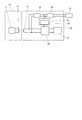
図1は、本発明による受電装置の構成を示すブロック図である。図1において、送電装置10は、少なくとも一次側制御部11と、受電装置20へ電力を供給するための送電アンテナ12を有する。受電装置20は、受電アンテナ21と、整流回路22と、スイッチ制御部23と、DC/DCコンバータ24と、スイッチ部26と、通信部27から構成される。スイッチ制御部23にはヒステリシス回路28を含み、DC/DCコンバータ24の出力には負荷25が接続される。スイッチ部26は、電力伝送時に受電アンテナ21及び整流回路22と、通信部27との接続を遮断することで過電圧から通信部27を保護する。
(Embodiment)
FIG. 1 is a block diagram showing a configuration of a power receiving device according to the present invention. In FIG. 1, the
受電アンテナ21は、送電装置10から磁気的な結合により送電された電力を交流電力として受電し、整流回路22に供給するとともに、一次側制御部11と信号を通信する際にも使用される。即ち、本実施の形態による受電アンテナ21は、電力の伝送と信号の通信とで共用される。
The
整流回路22は、受電アンテナ21で受電した交流電力を直流電力に変換する。DC/DCコンバータ24は、整流回路22で整流した直流電力の電圧を変換して負荷25に電力として供給する。
The
スイッチ制御部23は、ヒステリシス回路28を含み、整流回路22で整流した直流電力の電圧に応じて、スイッチ部26を導通状態にするか遮断状態にするかを制御する。
The
以下、本発明による受電装置の動作を説明する。 Hereinafter, the operation of the power receiving device according to the present invention will be described.
受電装置20が、一次側制御部11と通信可能な領域に置かれると、一次側制御部11と受電装置20の間でIDによる認証が行われる。このとき、スイッチ制御部23は、スイッチ部26を導通させ、受電アンテナ21と通信部27が電気的に接続されるよう制御する。
When the
認証が成功すると、一次側制御部11は受電装置20に対し、電力の伝送を開始する。受電アンテナ21で受電装置20に受電された電力は整流回路22で整流される。このとき、スイッチ制御部23は、後述の手順により整流後の電圧に応じてスイッチ部26を制御する。
When the authentication is successful, the primary
充電開始直後からDC/DCコンバータ24が動作するまでの間は、DC/DCコンバータ24の出力インピーダンスが一時的に高い状態になるため、整流回路22の出力電圧も一時的に上昇する。本発明による受電装置20は、この整流回路22の出力電圧が一時的に第1の閾値を越えるとスイッチ制御部23およびスイッチ部26を動作させる。第1の閾値は、充電開始直後の整流回路22の出力電圧と充電時の整流回路22の出力電圧の中間であればよい。
Since the output impedance of the DC /
すなわち、整流回路22の出力電圧が第1の閾値に達すると、スイッチ制御部は受電装置が信号を通信する状態から電力を伝送する状態に移行したとみなし、スイッチ部26を遮断する。すると、通信部27に電力は流れ込まない。
That is, when the output voltage of the
充電開始直後に一時的に上昇した整流回路22の出力電圧は、DC/DCコンバータ24が動作し始めるとともに出力インピーダンスが下がるため、整流回路22の出力電圧も下がる。受電アンテナ21で受電装置20に受電された電力は整流回路22で整流される。整流された電力はDC/DCコンバータ24を通して負荷25へ供給される。
The output voltage of the
所定の時間電力が伝送されると、一次側制御部11は充電を停止する。このとき、整流回路22の出力電圧はグランドレベルまで下降する。整流回路22の出力電圧が第2の閾値に到達したところで、受電装置20は一次側制御部が電力を伝送する状態から信号を通信する状態に移行したとみなし、スイッチ部26を導通させる。第2の閾値は、例えば、充電時の出力電圧の90%以下とすることができる。
When power is transmitted for a predetermined time, the
従って、整流回路22の出力電圧のレベルをスイッチ制御部23で検出し、整流回路の出力電圧が第1の閾値より大であればスイッチ部26を遮断することで通信部27を保護し、電力の受電を待機する。また、第2の閾値未満であれば電力伝送が終了したと判断し、通信部27の保護を解除するという動作を繰り返すことにより、信号の通信時の受電電圧と電力の伝送時の受電電圧の大小によらずに信号の通信と電力の伝送の判別が可能となる。
Therefore, the level of the output voltage of the
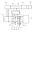
図2は、本発明による受電装置における、スイッチ部26の具体的な回路構成を示す図である。図2において、スイッチ部26は、受電アンテナ21と通信部27とを結ぶライン上に設けられたラインスイッチ部52と、各ラインとグランドとの間に設けられたグランドスイッチ部54とを備えている。ラインスイッチ部52及びグランドスイッチ部54は、NchのFETからなる。スイッチ部を構成するFETのドレインは、受電アンテナ21のコイルの一端に接続され、ソースは通信部27に接続され、ゲートはスイッチ制御部23に接続されている。グランドスイッチ部54を構成するFETのドレインは対応するラインに接続され、ソースはグランドに接続され、ゲートはスイッチ制御部23に接続されている。ツェナーダイオードZDは、対応するラインに接続されたカソードと、グランドに接続されたアノードとを有する。
FIG. 2 is a diagram showing a specific circuit configuration of the
かかる構成を有するスイッチ部によれば、ラインスイッチ部52を導通させると共にグランドスイッチ部54を遮断することで、受電アンテナ21と通信部27とを接続できる。また、スイッチ部を遮断すると共にグランドスイッチ部54を導通させることで、通信部27の入力をグランドレベルで短絡させることができ、受電アンテナ21から確実に切り離すことができる。
According to the switch unit having such a configuration, the
また、グランドスイッチ部54と並列に接続されたツェナーダイオードを設けても良い。ツェナーダイオードZDを備えることで、スイッチ部を導通状態から遮断状態へ移行するときも通信部27への入力電圧が一定レベル以上になることを防ぐことができる。すなわち、ツェナーダイオードZDは、スイッチ部に対して通信部27の入力保護機能を付加する。
Further, a Zener diode connected in parallel with the
図3は、本発明による受電装置におけるスイッチ部の第1の変形例を示す図である。スイッチ部26は、上述したものには限られず、スイッチ制御部23の制御に従って受電アンテナ21と通信部27との間を導通または遮断できるものであればよい。例えば、図2に示されるスイッチ部26においては、各ライン上にラインスイッチ部52を設けることとしていたが、図3に示されるスイッチ部26のように、一方のライン上に双方向スイッチ部56を設けてもよい。
FIG. 3 is a diagram illustrating a first modification of the switch unit in the power receiving device according to the present invention. The
図4は、本発明による受電装置におけるスイッチ部の第2の変形例を示す図である。図3において、スイッチ部26は、通信部27の入力を保護する入力保護部として双方向スイッチ部56が設けられたラインとグランドとの間に接続されたツェナーダイオードZDを有しているが、図4に示されるスイッチ部26のように、ツェナーダイオードZDを省略してもよい。図3に示されるスイッチ部26や図4に示されるスイッチ部26においても、信号時は双方向スイッチ部56を導通させる一方でグランドスイッチ部54を遮断することで、スイッチ部26を導通状態とし、電力伝送時は双方向スイッチ部56を遮断とする一方でグランドスイッチ部54を導通させることで、スイッチ部26を遮断状態とするように、スイッチ制御部23はスイッチ部26を制御する。
FIG. 4 is a diagram illustrating a second modification of the switch unit in the power receiving device according to the present invention. In FIG. 3, the
図5は、本発明による受電装置におけるスイッチ部の第3の変形例を示す図である。上述したスイッチ部26において、通信部27の入力を保護する入力保護部55はツェナーダイオードZDで構成されていたが、本発明はこれに限定されるわけではない。例えば、図5に示されるスイッチ部26は、ダイオードからなる入力保護部55−1を備えている。入力保護部55−1を構成するダイオードのアノードは、対応するラインに接続されており、同ダイオードのカソードはグランドに接続されている。かかる構成によれば、ダイオードの順電圧Vf以上の電圧が対応するラインに印加されると、ダイオードが導通し、通信部27が保護される。
FIG. 5 is a diagram showing a third modification of the switch unit in the power receiving device according to the present invention. In the
図6は、本発明による受電装置におけるスイッチ部の第4の変形例を示す図である。図6に示されるスイッチ部26のように、複数のダイオードを直列接続して入力保護部55−2を構成してもよい。
FIG. 6 is a diagram showing a fourth modification of the switch unit in the power receiving device according to the present invention. As in the
図6で図示されているように、直列接続された複数のダイオードの一端を構成するダイオードのアノードは対応するラインに接続されている一方、直列接続された複数のダイオードの他端を構成するダイオードのカソードはグランドに接続されている。同構成のダイオードを用いて入力保護部55−2を構成する場合、ダイオードの順電圧Vf×ダイオードの個数(直列数)で決まる電圧が入力保護部55−2の動作電圧となる。 As shown in FIG. 6, the anodes of the diodes constituting one end of the plurality of diodes connected in series are connected to the corresponding line, while the diodes constituting the other end of the plurality of diodes connected in series The cathode of is connected to ground. When the input protection unit 55-2 is configured using the diode having the same configuration, the voltage determined by the forward voltage Vf of the diode × the number of diodes (series number) becomes the operation voltage of the input protection unit 55-2.
また、複数種のダイオードを用いて入力保護部55−2を構成する場合、個々の入力保護部55−2の順電圧Vfの合計で決まる電圧が入力保護部55−2の動作電圧となる。このように、複数のダイオードを用いて入力保護部55−2を構成すると、入力保護部55−2の動作電圧を細かく設定することができる。 When the input protection unit 55-2 is configured using a plurality of types of diodes, the voltage determined by the sum of the forward voltages Vf of the individual input protection units 55-2 becomes the operating voltage of the input protection unit 55-2. Thus, when the input protection unit 55-2 is configured using a plurality of diodes, the operating voltage of the input protection unit 55-2 can be set finely.
このようにして設定された動作電圧以上の電圧がラインに印加されると、入力保護部55−2に電流が流れ、通信部27が保護される。
When a voltage equal to or higher than the set operating voltage is applied to the line, a current flows through the input protection unit 55-2, and the
図7は、本発明による受電装置の構成を示すブロック図であり、図1の変形例を示している。図1とは、受電アンテナ21と整流回路22の間にスイッチ部261を設け、通信部27からスイッチ制御部23への制御信号経路29を有している点が異なる。
FIG. 7 is a block diagram showing the configuration of the power receiving device according to the present invention, and shows a modification of FIG. 1 differs from FIG. 1 in that a
受電装置20が他のICカードやICタグと通信するような、受電装置20からの通信を行う場合がある。この場合は受電装置20がリーダライタのような機能を有することとなり、送電装置10が通信先のICカードやICタグ等に該当する。
There is a case where communication from the
このような受電装置20から送電装置10への通信を行う場合には、受電アンテナ21から通信信号を発信することになるため、整流回路22の出力電圧が、受電アンテナ21が通信信号を受信することを基に想定していた第1の閾値を超えてしまうことがある。
When communication from the
受電装置20から送電装置10への通信を行っている最中に整流回路22の出力電圧が第1の閾値を超してしまうと、スイッチ部26を遮断するため、受電アンテナ21から通信信号を出力できなくなってしまう。
If the output voltage of the
そこで、スイッチ制御部に予め第3の閾値を設定しておき、受電装置20から送電装置10への通信を行う場合のみ通信部27からスイッチ制御部23へ制御信号経路29を介して制御信号を伝達し、第1の閾値を第3の閾値に切り替えるよう構成すれば、受電装置20から送電装置10への通信を行っている最中にスイッチ部26による通信信号の遮断が起こらないため、上記のような問題が起こらない。
Therefore, a third threshold is set in advance in the switch control unit, and the control signal is transmitted from the
なお、第3の閾値は通信部27を保護できる上限の電圧と、受電装置20から送電装置10への通信による整流回路22の出力電圧の上限値の中間であればよい。
Note that the third threshold value may be between the upper limit voltage that can protect the
また、受電装置20と送電装置10の間で通信を行う場合に、DC/DCコンバータ24から負荷25に通信信号の電力が消費されることで充分な通信信号レベルを確保できない場合には、整流回路22とDC/DCコンバータ24の間に設けたスイッチ部261により、通信時のみ遮断するよう構成してもよい。
Further, when communication is performed between the
他に、スイッチ部261の開閉により負荷25への送電電力を変調することで、受電アンテナ21へ受電する際に負荷変調通信を行うこともできる。ここで、ICカードのようにスイッチ部261による負荷変調通信を行う場合は第1の閾値を採用し、ICカードに対するリーダライタのように通信部27からの通信信号の送受信を行う場合は第1の閾値を第3の閾値に変更することとしてもよい。
In addition, by modulating the transmission power to the
以上、この発明の実施の形態を説明したが、この発明は本実施例に限られるものではなく、この発明の要旨を逸脱しない範囲の設計変更があっても本発明に含まれる。 The embodiment of the present invention has been described above. However, the present invention is not limited to the present embodiment, and any design changes that do not depart from the gist of the present invention are included in the present invention.
本発明は、非接触充電機能を有する携帯電話機やデジタルカメラ等のような電子機器に適用可能であり、更に、それらを備えるシステムにも適用可能である。 The present invention can be applied to an electronic device such as a mobile phone or a digital camera having a non-contact charging function, and can also be applied to a system including them.
10 送電装置
11 一次側制御部
12 送電アンテナ
20 受電装置
21 受電アンテナ
22 整流回路
23 スイッチ制御部
24 DC/DCコンバータ
25 負荷
26、261 スイッチ部
27 通信部
28 ヒステリシス回路
29 制御信号経路
52 ラインスイッチ部
54 グランドスイッチ部
55、55−1、55−2 入力保護部
56 双方向スイッチ部
D ドレイン
G ゲート
S ソース
ZD ツェナーダイオード
DESCRIPTION OF
Claims (10)
前記電力を直流電圧に変換する整流回路と、
前記通信信号を処理する通信部と、
前記通信部を保護するスイッチ部と、
前記整流回路の出力に応じて前記スイッチ部を制御するスイッチ制御部とを少なくとも備え、
前記スイッチ制御部の切り替えの閾値は、通信から充電に切り替える時の第1の閾値と充電から通信に切り替える第2の閾値が異なることを特徴とする受電装置。 A power receiving antenna intends line transmission of the transmission and the power of the communication signal,
A rectifier circuit for converting the power into a DC voltage ;
A communication unit for processing the communication signal,
A switch unit for protecting the communication unit;
A switch control unit that controls the switch unit according to the output of the rectifier circuit,
The power receiving apparatus according to claim 1, wherein the switching threshold value of the switch control unit is different from a first threshold value when switching from communication to charging and a second threshold value switching from charging to communication.
前記第3の閾値の絶対値は前記第1の閾値の絶対値よりも大であることを特徴とする請求項1から請求項3のいずれかに記載の受電装置。 When transmitting a communication signal from the power receiving antenna, the first threshold value is switched to a third threshold value,
The third of the absolute value of the threshold power receiving device according to any one of claims 1 to 3, characterized in that is larger than the absolute value of the first threshold value.
前記第1の閾値であり、
前記受電アンテナより通信信号を送信する場合には、前記第1の閾値を第3の閾値に切り替え、
前記第3の閾値の絶対値は前記第1の閾値の絶対値よりも大であることを特徴とする請求項1から請求項4のいずれかに記載の受電装置。 When performing communication by performing load modulation from the power receiving antenna, or the threshold for receiving,
The first threshold;
When transmitting a communication signal from the power receiving antenna, the first threshold value is switched to a third threshold value,
The third of the absolute value of the threshold power receiving device according to any one of claims 1 to 4, characterized in that is larger than the absolute value of the first threshold value.
The power receiving device according to claim 8, wherein the line switch unit and the ground switch unit are configured by Nch FETs.
Priority Applications (6)
| Application Number | Priority Date | Filing Date | Title |
|---|---|---|---|
| JP2012266851A JP6073663B2 (en) | 2012-02-24 | 2012-12-06 | Power receiving device and electronic device |
| US14/371,141 US9837858B2 (en) | 2012-12-06 | 2013-06-28 | Power reception device and electronic apparatus |
| KR1020147014254A KR20150091222A (en) | 2012-12-06 | 2013-06-28 | Power receiving device and electronic apparatus |
| PCT/JP2013/067784 WO2014087692A1 (en) | 2012-12-06 | 2013-06-28 | Power receiving apparatus and electronic apparatus |
| TW102124743A TW201424185A (en) | 2012-12-06 | 2013-07-10 | Power receving device and electronic equipment |
| US15/703,183 US20180006507A1 (en) | 2012-12-06 | 2017-09-13 | Power reception device and electronic apparatus |
Applications Claiming Priority (3)
| Application Number | Priority Date | Filing Date | Title |
|---|---|---|---|
| JP2012039011 | 2012-02-24 | ||
| JP2012039011 | 2012-02-24 | ||
| JP2012266851A JP6073663B2 (en) | 2012-02-24 | 2012-12-06 | Power receiving device and electronic device |
Publications (3)
| Publication Number | Publication Date |
|---|---|
| JP2013201881A JP2013201881A (en) | 2013-10-03 |
| JP2013201881A5 JP2013201881A5 (en) | 2016-01-21 |
| JP6073663B2 true JP6073663B2 (en) | 2017-02-01 |
Family
ID=50883810
Family Applications (1)
| Application Number | Title | Priority Date | Filing Date |
|---|---|---|---|
| JP2012266851A Expired - Fee Related JP6073663B2 (en) | 2012-02-24 | 2012-12-06 | Power receiving device and electronic device |
Country Status (5)
| Country | Link |
|---|---|
| US (2) | US9837858B2 (en) |
| JP (1) | JP6073663B2 (en) |
| KR (1) | KR20150091222A (en) |
| TW (1) | TW201424185A (en) |
| WO (1) | WO2014087692A1 (en) |
Families Citing this family (7)
| Publication number | Priority date | Publication date | Assignee | Title |
|---|---|---|---|---|
| JP5308588B1 (en) * | 2013-04-26 | 2013-10-09 | Necトーキン株式会社 | Power receiving device and electronic device |
| DE102013105291B4 (en) * | 2013-05-23 | 2017-12-07 | Infineon Technologies Ag | smart card |
| JP2017536792A (en) | 2014-10-01 | 2017-12-07 | ヒューマヴォックス リミテッド | RF charging / communication composite module and method of use |
| KR101678989B1 (en) * | 2015-06-29 | 2016-11-25 | 주식회사 맵스 | Protection apparatus for communication system by magnetic field and mobile terminal thereof |
| CN110546853A (en) * | 2017-04-24 | 2019-12-06 | 三菱电机工程技术株式会社 | Resonance type power receiving device |
| JP7187135B2 (en) * | 2017-05-16 | 2022-12-12 | ラピスセミコンダクタ株式会社 | Wireless power receiving device, wireless power supply device, wireless power transmission system, and excessive magnetic field protection method for wireless power receiving device |
| KR20210146571A (en) * | 2020-05-27 | 2021-12-06 | 삼성전자주식회사 | Electronic device for wirelessly receiving power and method for operating thereof |
Family Cites Families (18)
| Publication number | Priority date | Publication date | Assignee | Title |
|---|---|---|---|---|
| US5933263A (en) * | 1997-02-14 | 1999-08-03 | The Boeing Company | Self-powered datalink activation system |
| EP1458083B1 (en) * | 1999-06-09 | 2012-04-04 | Lear Corporation Holding Spain S.L. | Dual voltage electrical distribution system |
| DE19957478A1 (en) * | 1999-11-23 | 2001-05-31 | Volkswagen Ag | Two battery system for vehicle has power switch connected between system battery and starter battery that can be controlled by signal detecting generator stimulation |
| JP2003158468A (en) * | 2001-11-20 | 2003-05-30 | Toshiba Corp | Portable radio equipment |
| JP4622645B2 (en) * | 2005-04-15 | 2011-02-02 | トヨタ自動車株式会社 | Battery device, internal combustion engine device including the same, and vehicle |
| JP4756590B2 (en) * | 2005-12-28 | 2011-08-24 | 本田技研工業株式会社 | Vehicle power supply device |
| US7986122B2 (en) * | 2007-09-26 | 2011-07-26 | Enphase Energy, Inc. | Method and apparatus for power conversion with maximum power point tracking and burst mode capability |
| JP4591630B2 (en) * | 2008-09-29 | 2010-12-01 | 株式会社村田製作所 | Contactless power receiving circuit and contactless power transmission system |
| US20110115303A1 (en) * | 2009-11-19 | 2011-05-19 | Access Business Group International Llc | Multiple use wireless power systems |
| JP5387387B2 (en) * | 2009-12-24 | 2014-01-15 | 株式会社村田製作所 | Electronic medium with IC and electronic medium system with IC |
| US9502904B2 (en) * | 2010-03-23 | 2016-11-22 | Eaton Corporation | Power conversion system and method providing maximum efficiency of power conversion for a photovoltaic system, and photovoltaic system employing a photovoltaic array and an energy storage device |
| JP2012039707A (en) * | 2010-08-05 | 2012-02-23 | Panasonic Corp | Non-contact charging device |
| US9219378B2 (en) * | 2010-11-01 | 2015-12-22 | Qualcomm Incorporated | Wireless charging of devices |
| FR2967857B1 (en) * | 2010-11-19 | 2014-08-22 | Eads Defence & Security Sys | METHOD FOR MANAGING THE BATTERY LEVEL OF A MOBILE TERMINAL, CORRESPONDING MANAGEMENT SYSTEM AND COMPUTER PROGRAM |
| JP5325347B2 (en) | 2010-12-27 | 2013-10-23 | Necトーキン株式会社 | Electronic devices, modules and systems |
| JP5677875B2 (en) | 2011-03-16 | 2015-02-25 | 日立マクセル株式会社 | Non-contact power transmission system |
| JP5488578B2 (en) * | 2011-12-19 | 2014-05-14 | 株式会社デンソー | Electric refrigeration cycle equipment for vehicles |
| US8683090B2 (en) * | 2012-04-19 | 2014-03-25 | Apple Inc. | Methods, systems and apparatus for determining whether an accessory includes particular circuitry |
-
2012
- 2012-12-06 JP JP2012266851A patent/JP6073663B2/en not_active Expired - Fee Related
-
2013
- 2013-06-28 KR KR1020147014254A patent/KR20150091222A/en not_active Application Discontinuation
- 2013-06-28 WO PCT/JP2013/067784 patent/WO2014087692A1/en active Application Filing
- 2013-06-28 US US14/371,141 patent/US9837858B2/en not_active Expired - Fee Related
- 2013-07-10 TW TW102124743A patent/TW201424185A/en unknown
-
2017
- 2017-09-13 US US15/703,183 patent/US20180006507A1/en not_active Abandoned
Also Published As
| Publication number | Publication date |
|---|---|
| US9837858B2 (en) | 2017-12-05 |
| KR20150091222A (en) | 2015-08-10 |
| US20150042170A1 (en) | 2015-02-12 |
| TW201424185A (en) | 2014-06-16 |
| US20180006507A1 (en) | 2018-01-04 |
| JP2013201881A (en) | 2013-10-03 |
| WO2014087692A1 (en) | 2014-06-12 |
Similar Documents
| Publication | Publication Date | Title |
|---|---|---|
| JP6073663B2 (en) | Power receiving device and electronic device | |
| JP6087740B2 (en) | Communication device | |
| US9361564B2 (en) | Protection of an NFC or RFID radio in the presence of strong electromagnetic fields | |
| JP5308588B1 (en) | Power receiving device and electronic device | |
| JP5325347B2 (en) | Electronic devices, modules and systems | |
| US9306400B2 (en) | Power transmission device and waveform monitor circuit for use in power transmission device | |
| JP5998905B2 (en) | Wireless power receiving apparatus and wireless power transmission apparatus using the same | |
| JP5551465B2 (en) | Contactless power transmission and communication system | |
| US10483797B2 (en) | Contactless connector and contactless connector system | |
| EP3195492B1 (en) | Overvoltage protection for nfc devices | |
| US20150098162A1 (en) | Apparatus and Methods of Bootstrap and Over Voltage Combination Clamp for Wireless Power Receiver | |
| US9972903B2 (en) | Communication device | |
| US20150097439A1 (en) | Apparatus and Methods of N-Type Load Switch Using Bootstrap Gate Drive for Wireless Power Receiver | |
| JP5481598B1 (en) | Communication device | |
| US20160087479A1 (en) | Receiver circuit | |
| KR20160010283A (en) | Communication apparatus and electronic device | |
| JP6276128B2 (en) | Portable terminal, control method, and charging system | |
| KR20130099150A (en) | Electronic equipment and system |
Legal Events
| Date | Code | Title | Description |
|---|---|---|---|
| A521 | Request for written amendment filed |
Free format text: JAPANESE INTERMEDIATE CODE: A523 Effective date: 20131106 |
|
| A521 | Request for written amendment filed |
Free format text: JAPANESE INTERMEDIATE CODE: A523 Effective date: 20151201 |
|
| A621 | Written request for application examination |
Free format text: JAPANESE INTERMEDIATE CODE: A621 Effective date: 20151201 |
|
| RD03 | Notification of appointment of power of attorney |
Free format text: JAPANESE INTERMEDIATE CODE: A7423 Effective date: 20151201 |
|
| TRDD | Decision of grant or rejection written | ||
| A01 | Written decision to grant a patent or to grant a registration (utility model) |
Free format text: JAPANESE INTERMEDIATE CODE: A01 Effective date: 20161214 |
|
| A61 | First payment of annual fees (during grant procedure) |
Free format text: JAPANESE INTERMEDIATE CODE: A61 Effective date: 20170105 |
|
| R150 | Certificate of patent or registration of utility model |
Ref document number: 6073663 Country of ref document: JP Free format text: JAPANESE INTERMEDIATE CODE: R150 |
|
| S533 | Written request for registration of change of name |
Free format text: JAPANESE INTERMEDIATE CODE: R313533 |
|
| R350 | Written notification of registration of transfer |
Free format text: JAPANESE INTERMEDIATE CODE: R350 |
|
| LAPS | Cancellation because of no payment of annual fees |