JP6069719B2 - Software debugging method, information processing apparatus, and program - Google Patents

Software debugging method, information processing apparatus, and program Download PDF

Info

Publication number
JP6069719B2
JP6069719B2 JP2015529270A JP2015529270A JP6069719B2 JP 6069719 B2 JP6069719 B2 JP 6069719B2 JP 2015529270 A JP2015529270 A JP 2015529270A JP 2015529270 A JP2015529270 A JP 2015529270A JP 6069719 B2 JP6069719 B2 JP 6069719B2
Authority
JP
Japan
Prior art keywords
information
instruction
cpu
area
address
Prior art date
Legal status (The legal status is an assumption and is not a legal conclusion. Google has not performed a legal analysis and makes no representation as to the accuracy of the status listed.)
Active
Application number
JP2015529270A
Other languages
Japanese (ja)
Other versions
JPWO2015015591A1 (en
Inventor
良行 大平
良行 大平
Current Assignee (The listed assignees may be inaccurate. Google has not performed a legal analysis and makes no representation or warranty as to the accuracy of the list.)
Fujitsu Ltd
Original Assignee
Fujitsu Ltd
Priority date (The priority date is an assumption and is not a legal conclusion. Google has not performed a legal analysis and makes no representation as to the accuracy of the date listed.)
Filing date
Publication date
Application filed by Fujitsu Ltd filed Critical Fujitsu Ltd
Application granted granted Critical
Publication of JP6069719B2 publication Critical patent/JP6069719B2/en
Publication of JPWO2015015591A1 publication Critical patent/JPWO2015015591A1/en
Active legal-status Critical Current
Anticipated expiration legal-status Critical

Links

Images

Classifications

    • GPHYSICS
    • G06COMPUTING; CALCULATING OR COUNTING
    • G06FELECTRIC DIGITAL DATA PROCESSING
    • G06F11/00Error detection; Error correction; Monitoring
    • G06F11/36Preventing errors by testing or debugging software
    • G06F11/362Software debugging

Description

本発明はソフトウェアデバッグ方法、情報処理装置およびプログラムに関する。   The present invention relates to a software debugging method, an information processing apparatus, and a program.

コンピュータで実行されるソフトウェアが途中で異常停止・異常終了するなど、ソフトウェアの動作に仕様と異なる不具合(バグ)が含まれていることがあり、その不具合を検出し修正するためにデバッグ作業が行われる。デバッグ作業では、不具合の発生状況を示す情報(例えば、エラーログやメモリダンプなど)を収集し、収集した情報を分析してその不具合の原因を特定し、ソフトウェアの修正(例えば、ソースコードの書き換え)を行う。   The software running on the computer may stop abnormally or terminate abnormally, and the software operation may contain a bug (bug) that differs from the specification. Debugging is performed to detect and fix the bug. Is called. In debugging, information that indicates the occurrence of a problem (for example, an error log or memory dump) is collected, the collected information is analyzed to identify the cause of the problem, and software correction (for example, rewriting of the source code) is performed. )I do.

ここで、複数のプロセッサ(プロセッサコアと呼ばれるものを含む)でソフトウェアを並列に動作させる場合、1つのプロセッサのみでソフトウェアを動作させる場合とは異なる環境条件によって不具合が発生し得る。そのような不具合の原因の一例として、メモリ上の領域に対する排他制御の不備が挙げられる。メモリ上の領域を使用するとき適切にロックが獲得されないと、2つ以上のプロセッサが同時期に同じメモリアドレスの領域にアクセスし、あるプロセッサの使用するデータが他のプロセッサによって意図せず書き換えられてしまうことがある。   Here, when software is operated in parallel by a plurality of processors (including what is called a processor core), problems may occur due to environmental conditions different from the case where software is operated by only one processor. One example of the cause of such a problem is a lack of exclusive control over an area on the memory. If a lock is not properly acquired when using a memory area, two or more processors access the same memory address area at the same time, and the data used by one processor is unintentionally rewritten by another processor. May end up.

例えば、あるプロセッサが、ある変数に一時的に値を代入してからその値を読み出すとする。変数への値の代入と変数からの値の読み出しの間に、排他制御が適切に行われずに他のプロセッサによって当該変数の値が書き換えられてしまうと、当該プロセッサの処理で異常が発生することがある。このような排他制御の不備に基づく不具合は、各プロセッサにおける命令の実行タイミングにも依存するため再現率が低くなることがあり、デバッグ作業においてその原因を特定することが容易でないことが多い。   For example, assume that a processor temporarily assigns a value to a variable and then reads the value. If the value of the variable is rewritten by another processor without appropriate exclusive control between the assignment of the value to the variable and the reading of the value from the variable, an abnormality occurs in the processing of the processor There is. Such inconveniences due to the lack of exclusive control depend on the instruction execution timing in each processor, so the recall rate may be low, and it is often difficult to identify the cause in debugging work.

そこで、例えば、ソフトウェアとしてのシミュレータ上に、仮想的なプロセッサや仮想的なメモリなどのハードウェアモデルを構築し、シミュレータ上で並列プログラムを実行するシミュレーション方法が提案されている。このシミュレーション方法では、シミュレータ上で並列プログラムを実行する間、仮想的なメモリモニタが、各プロセッサからメモリへのアクセスについての情報を収集する。そして、メモリモニタが、収集した情報に基づいて、複数のプロセッサが重複してアクセスしたメモリ領域を特定する。   Thus, for example, a simulation method has been proposed in which a hardware model such as a virtual processor or virtual memory is constructed on a simulator as software, and a parallel program is executed on the simulator. In this simulation method, while a parallel program is executed on the simulator, a virtual memory monitor collects information about access to the memory from each processor. Then, the memory monitor identifies the memory area accessed by the plurality of processors in an overlapping manner based on the collected information.

また、例えば、プロセッサおよびメモリが接続されたバスに、ハードウェアとしてのメモリ監視回路を設けたデータ処理装置が提案されている。このメモリ監視回路は、ユーザから指定された所定のアドレス範囲の領域について、メモリへのアクセスを監視する。メモリ監視回路は、データ書込用のカウンタとデータ読込用のカウンタとを有し、所定のアドレス範囲の領域に対するデータ書込およびデータ読込の回数をそれぞれカウントする。カウンタの値は、メモリ監視回路から分析ロジックに出力される。   For example, a data processing device has been proposed in which a memory monitoring circuit as hardware is provided on a bus to which a processor and a memory are connected. This memory monitoring circuit monitors access to the memory in a predetermined address range designated by the user. The memory monitoring circuit has a data write counter and a data read counter, and counts the number of times data is written to and read from an area in a predetermined address range. The counter value is output from the memory monitoring circuit to the analysis logic.

特開2009−32197号公報JP 2009-32197 A 特開2010−20767号公報JP 2010-20767 A

しかし、メモリアクセスの情報を収集して排他制御の不備を判定するために、上記のような特殊なシミュレーション環境または特殊なハードウェアを使用することは、デバッグ作業の負担が大きくなることがあるという問題がある。デバッグ作業時の環境によっては、デバッグ対象のソフトウェアが動作する本番システムまたは本番環境と同等のハードウェア構成のシステムのもとで、デバッグ作業を実施したいことがある。   However, using a special simulation environment or special hardware as described above to collect memory access information and determine the lack of exclusive control may increase the burden of debugging. There's a problem. Depending on the environment at the time of debugging, it may be desired to perform the debugging work under a production system in which the software to be debugged operates or a system having a hardware configuration equivalent to the production environment.

1つの側面では、本発明は、メモリに対する排他制御の不備の判定を容易にするソフトウェアデバッグ方法、情報処理装置およびプログラムを提供することを目的とする。   In one aspect, an object of the present invention is to provide a software debugging method, an information processing apparatus, and a program that facilitate determination of incompleteness of exclusive control over a memory.

1つの態様では、複数のプロセッサを含むコンピュータが実行するソフトウェアデバッグ方法が提供される。第1および第2のプロセッサそれぞれが、命令の実行を制御する制御ソフトウェアを用いて、デバッグするソフトウェアに含まれる命令を実行する。第1のプロセッサが、メモリに対するデータ書込またはデータ参照を示す第1の命令を実行するとき、第1の命令に応じた第1の履歴情報を生成する。第2のプロセッサが、メモリに対するデータ書込を示す第2の命令を実行するとき、第2の命令に応じた第2の履歴情報を生成する。第1のプロセッサが、第2の履歴情報を取得し、第1および第2の履歴情報に基づいて、メモリ上の領域に対する排他制御の不備を判定する。   In one aspect, a software debugging method executed by a computer including a plurality of processors is provided. Each of the first and second processors executes instructions included in the software to be debugged using control software that controls execution of the instructions. When the first processor executes a first instruction indicating data writing or data reference to the memory, the first processor generates first history information according to the first instruction. When the second processor executes a second instruction indicating data writing to the memory, the second processor generates second history information according to the second instruction. The first processor acquires the second history information, and determines the lack of exclusive control for the area on the memory based on the first and second history information.

また、1つの態様では、命令の実行を制御する制御ソフトウェアを用いて、デバッグするソフトウェアに含まれる命令を実行する第1および第2のプロセッサと、第1および第2のプロセッサからアクセスされるメモリと、を有する情報処理装置が提供される。第1のプロセッサは、メモリに対するデータ書込またはデータ参照を示す第1の命令を実行するとき、第1の命令に応じた第1の履歴情報を生成する。第2のプロセッサは、メモリに対するデータ書込を示す第2の命令を実行するとき、第2の命令に応じた第2の履歴情報を生成する。第1のプロセッサは、第2の履歴情報を取得し、第1および第2の履歴情報に基づいて、メモリ上の領域に対する排他制御の不備を判定する。   In one aspect, the control software that controls the execution of the instructions, the first and second processors that execute the instructions included in the software to be debugged, and the memory that is accessed from the first and second processors Is provided. When the first processor executes a first instruction indicating data writing or data reference to the memory, the first processor generates first history information corresponding to the first instruction. When the second processor executes a second instruction indicating data writing to the memory, the second processor generates second history information corresponding to the second instruction. The first processor acquires the second history information, and determines the lack of exclusive control for the area on the memory based on the first and second history information.

また、1つの態様では、複数のプロセッサを含むコンピュータに、次の処理を実行させるプログラムが提供される。第1および第2のプロセッサそれぞれにおいて、デバッグするソフトウェアに含まれる命令が実行されるように制御する。第1のプロセッサを用いて、メモリに対するデータ書込またはデータ参照を示す第1の命令が実行されるとき、第1の命令に応じた第1の履歴情報を生成する。第2のプロセッサを用いて、メモリに対するデータ書込を示す第2の命令が実行されるとき、第2の命令に応じた第2の履歴情報を生成する。第1のプロセッサを用いて、第2の履歴情報を取得し、第1および第2の履歴情報に基づいて、メモリ上の領域に対する排他制御の不備を判定する。   Moreover, in one aspect, a program for causing a computer including a plurality of processors to execute the following processing is provided. In each of the first and second processors, control is performed so that instructions included in the software to be debugged are executed. When a first instruction indicating data writing or data reference to the memory is executed using the first processor, first history information corresponding to the first instruction is generated. When a second instruction indicating data writing to the memory is executed using the second processor, second history information corresponding to the second instruction is generated. Using the first processor, the second history information is acquired, and based on the first and second history information, it is determined whether the exclusive control for the area on the memory is insufficient.

1つの側面では、メモリに対する排他制御の不備の判定が容易になる。
本発明の上記および他の目的、特徴および利点は本発明の例として好ましい実施の形態を表す添付の図面と関連した以下の説明により明らかになるであろう。
In one aspect, it is easy to determine the lack of exclusive control for the memory.
These and other objects, features and advantages of the present invention will become apparent from the following description taken in conjunction with the accompanying drawings which illustrate preferred embodiments by way of example of the present invention.

第1の実施の形態の情報処理装置を示す図である。It is a figure which shows the information processing apparatus of 1st Embodiment. 情報処理装置のハードウェア例を示すブロック図である。And FIG. 11 is a block diagram illustrating a hardware example of an information processing apparatus. ソフトウェアの階層例を示す図である。It is a figure which shows the hierarchy example of software. データ書込時の排他制御不備の例を示す図である。It is a figure which shows the example of the exclusive control defect at the time of data writing. データ書込時の排他制御不備の検出例を示すシーケンス図である。It is a sequence diagram which shows the detection example of the exclusive control defect at the time of data writing. 排他制御不備の有無の判定例を示す図である。It is a figure which shows the example of determination of the presence or absence of exclusive control defect. 情報処理装置の機能例を示すブロック図である。It is a block diagram which shows the function example of information processing apparatus. 第2の実施の形態の制御情報の全体構造例を示す図である。It is a figure which shows the example of whole structure of the control information of 2nd Embodiment. 第2の実施の形態の管理情報のデータ構造例を示す図である。It is a figure which shows the data structure example of the management information of 2nd Embodiment. 第1のポインタテーブルのデータ構造例を示す図である。It is a figure which shows the example of a data structure of a 1st pointer table. 収集領域のデータ構造例を示す図である。It is a figure which shows the data structure example of a collection area | region. 収集領域ヘッダのデータ構造例を示す図である。It is a figure which shows the data structure example of a collection area header. 集計領域のデータ構造例を示す図である。It is a figure which shows the example of a data structure of a total area. 書込ビットマップのデータ構造例を示す図である。It is a figure which shows the example of a data structure of a write bit map. 追記領域のデータ構造例を示す図である。It is a figure which shows the example of a data structure of an additional recording area | region. 第2のポインタテーブルのデータ構造例を示す図である。It is a figure which shows the example of a data structure of a 2nd pointer table. ログ管理情報のデータ構造例を示す図である。It is a figure which shows the example of a data structure of log management information. 第2の実施の形態のログ情報のデータ構造例を示す図である。It is a figure which shows the example of a data structure of the log information of 2nd Embodiment. 起動処理および停止処理の手順例を示すフローチャートである。It is a flowchart which shows the example of a procedure of a starting process and a stop process. データ書込時のデバッグ支援の手順例を示すフローチャートである。It is a flowchart which shows the example of a procedure of the debugging assistance at the time of data writing. アドレス情報収集の手順例を示すフローチャートである。It is a flowchart which shows the example of a procedure of address information collection. ロック獲得記録の手順例を示すフローチャートである。It is a flowchart which shows the example of a procedure of lock acquisition recording. ロック解放判定の手順例を示すフローチャートである。It is a flowchart which shows the example of a procedure of lock release determination. 排他制御不備検出の手順例を示すフローチャートである。It is a flowchart which shows the example of a procedure of exclusive control defect detection. 排他制御不備検出の手順例を示すフローチャート(続き)である。It is a flowchart (continuation) which shows the example of a procedure of exclusive control defect detection. 書込衝突判定の手順例を示すフローチャートである。It is a flowchart which shows the example of a procedure of writing collision determination. データ参照時の排他制御不備の例を示す図である。It is a figure which shows the example of the exclusive control defect at the time of data reference. データ参照時の排他制御不備の検出例を示すシーケンス図である。It is a sequence diagram which shows the detection example of the exclusive control defect at the time of data reference. 第3の実施の形態の制御情報の全体構造例を示す図である。It is a figure which shows the example of whole structure of the control information of 3rd Embodiment. 第3の実施の形態の管理情報のデータ構造例を示す図である。It is a figure which shows the example of a data structure of the management information of 3rd Embodiment. 第3のポインタテーブルのデータ構造例を示す図である。It is a figure which shows the example of a data structure of a 3rd pointer table. 収集依頼情報のデータ構造例を示す図である。It is a figure which shows the example of a data structure of collection request information. 比較命令情報のデータ構造例を示す図である。It is a figure which shows the data structure example of comparison command information. 第4のポインタテーブルのデータ構造例を示す図である。It is a figure which shows the example of a data structure of a 4th pointer table. 衝突情報のデータ構造例を示す図である。It is a figure which shows the data structure example of collision information. 第3の実施の形態のログ情報のデータ構造例を示す図である。It is a figure which shows the data structure example of the log information of 3rd Embodiment. データ参照時のデバッグ支援の手順例を示すフローチャートである。It is a flowchart which shows the example of a procedure of the debugging assistance at the time of data reference. 衝突情報収集の手順例を示すフローチャートである。It is a flowchart which shows the example of a procedure of collision information collection. 読み書き衝突判定の手順例を示すフローチャートである。It is a flowchart which shows the example of a procedure of read / write collision determination. データ参照時の排他制御不備検出の手順例を示すフローチャートである。It is a flowchart which shows the example of a procedure of exclusive control defect detection at the time of data reference.

以下、本実施の形態を図面を参照して説明する。
[第1の実施の形態]
図1は、第1の実施の形態の情報処理装置を示す図である。
Hereinafter, the present embodiment will be described with reference to the drawings.
[First Embodiment]
FIG. 1 is a diagram illustrating the information processing apparatus according to the first embodiment.

第1の実施の形態の情報処理装置10は、デバッグ対象のソフトウェアとして、複数のプロセッサを使用して並列処理を行うソフトウェアを実行できる。このソフトウェアは、OS(Operating System)やデバイスドライバなどのシステムプログラムを含んでもよいし、システムプログラム上で動作するユーザプログラムを含んでもよい。   The information processing apparatus 10 according to the first embodiment can execute software that performs parallel processing using a plurality of processors as software to be debugged. This software may include a system program such as an OS (Operating System) and a device driver, or may include a user program that operates on the system program.

情報処理装置10は、プロセッサ11,12およびメモリ13を有する。プロセッサ11,12は、メモリ13を用いて、算術演算命令・論理演算命令・比較命令・分岐命令・データ転送命令などの各種の命令を実行する。プロセッサ11,12それぞれは、CPU(Central Processing Unit)などのプロセッサパッケージでもよいし、プロセッサパッケージ内のプロセッサコアであってもよい。メモリ13は、プロセッサ11,12からアクセスされる共有メモリであり、例えば、RAM(Random Access Memory)である。   The information processing apparatus 10 includes processors 11 and 12 and a memory 13. The processors 11 and 12 use the memory 13 to execute various instructions such as arithmetic operation instructions, logical operation instructions, comparison instructions, branch instructions, and data transfer instructions. Each of the processors 11 and 12 may be a processor package such as a CPU (Central Processing Unit), or may be a processor core in the processor package. The memory 13 is a shared memory accessed from the processors 11 and 12, and is, for example, a RAM (Random Access Memory).

ここで、プロセッサ11,12それぞれは、命令の実行を制御する制御ソフトウェア14を用いて、デバッグ対象のソフトウェアに含まれる命令を実行する。制御ソフトウェア14は、例えば、エミュレータと呼ばれるものである。エミュレータは、デバッグ対象のソフトウェアが使用する命令セットとプロセッサ11,12が解釈可能な命令セットとが異なる場合に、前者の命令セットを後者の命令セットに変換する。エミュレータは、ハードウェアとソフトウェアの間の命令セットの違いを吸収していると言うこともできる。   Here, each of the processors 11 and 12 executes an instruction included in the software to be debugged using the control software 14 that controls the execution of the instruction. The control software 14 is called an emulator, for example. The emulator converts the former instruction set into the latter instruction set when the instruction set used by the software to be debugged is different from the instruction set interpretable by the processors 11 and 12. It can also be said that the emulator absorbs the difference in instruction set between hardware and software.

第1の実施の形態では、制御ソフトウェア14には、デバッグ作業を支援するため、メモリ13上の領域に対する排他制御の不備を判定する機能が実装される。メモリ13上のある領域を使用するときに適切にロックが獲得されないと、プロセッサ11,12が同時期に同じメモリアドレスの領域にアクセスし、プロセッサ11で使用されているデータがプロセッサ12によって意図せず破壊されてしまうことがある。排他制御の不備によって不具合が発生する場合として、例えば、プロセッサ11とプロセッサ12が同じ領域に対して同時期にデータを書き込む場合が挙げられる。また、不具合が発生する他の場合として、例えば、プロセッサ11がメモリ13上の複数のブロックに跨がるデータを参照している間に、プロセッサ12がそのうちの1つのブロックのデータを書き換えてしまう場合が挙げられる。   In the first embodiment, the control software 14 is equipped with a function for determining the lack of exclusive control for an area on the memory 13 in order to support debugging work. If a lock is not properly acquired when a certain area on the memory 13 is used, the processors 11 and 12 access the area having the same memory address at the same time, and the data used in the processor 11 is intended by the processor 12. It may be destroyed. As a case where a defect occurs due to inadequate exclusive control, for example, there is a case where the processor 11 and the processor 12 write data to the same area at the same time. As another case where a failure occurs, for example, the processor 12 rewrites data in one of the blocks while the processor 11 is referring to data across a plurality of blocks on the memory 13. There are cases.

そこで、プロセッサ11,12は、デバッグ対象のソフトウェアを実行する間、制御ソフトウェア14の制御に従って次のような処理を行う。プロセッサ11は、デバッグ対象のソフトウェアに含まれる命令のうち、メモリ13に対するデータ書込またはデータ参照を伴う命令15を実行するとき、命令15に応じた履歴情報17を生成する。データ書込を伴う命令の一例としては、ストア命令が挙げられ、データ参照を伴う命令の一例としては、メモリ13上のデータを利用する比較命令が挙げられる。履歴情報17は、アクセスされるメモリ13の領域を示すアドレス情報を含んでもよい。また、履歴情報17は、命令15が属するプログラムモジュールの識別情報を含んでもよい。生成された履歴情報17は、例えば、メモリ13上に予め設けられたプロセッサ11用の領域に格納される。   Therefore, the processors 11 and 12 perform the following processing according to the control of the control software 14 while executing the debug target software. The processor 11 generates the history information 17 corresponding to the instruction 15 when executing the instruction 15 that involves writing or referring to the memory 13 among the instructions included in the software to be debugged. An example of an instruction involving data writing is a store instruction, and an example of an instruction involving data reference is a comparison instruction using data on the memory 13. The history information 17 may include address information indicating an area of the memory 13 to be accessed. The history information 17 may include identification information of the program module to which the instruction 15 belongs. The generated history information 17 is stored in an area for the processor 11 provided in advance on the memory 13, for example.

また、プロセッサ12は、デバッグ対象のソフトウェアに含まれる命令のうち、メモリ13に対するデータ書込を伴う命令16を実行するとき、命令16に応じた履歴情報18を生成する。履歴情報18は、アクセスされるメモリ13の領域を示すアドレス情報を含んでもよい。また、履歴情報18は、命令16が属するプログラムモジュールの識別情報を含んでもよい。生成された履歴情報18は、例えば、メモリ13上に予め設けられたプロセッサ11用の領域およびプロセッサ12用の領域の少なくとも一方に格納される。   Further, the processor 12 generates history information 18 corresponding to the instruction 16 when executing the instruction 16 accompanied by data writing to the memory 13 among the instructions included in the debug target software. The history information 18 may include address information indicating an area of the memory 13 to be accessed. The history information 18 may include identification information of a program module to which the instruction 16 belongs. The generated history information 18 is stored, for example, in at least one of an area for the processor 11 and an area for the processor 12 provided in advance on the memory 13.

そして、プロセッサ11は、プロセッサ12が生成した履歴情報18を収集し、生成した履歴情報17と収集した履歴情報18とに基づいて、デバッグ対象のソフトウェアに排他制御の不備があるか判定する。履歴情報17,18は、例えば、メモリ13上に予め設けられたプロセッサ11用の領域に集められる。プロセッサ11は、例えば、履歴情報17が示すアドレスと履歴情報18が示すアドレスとを比較し、履歴情報17,18が同一または近いアドレスを指し示しているとき、排他制御の不備があると判定する。   Then, the processor 11 collects the history information 18 generated by the processor 12 and determines whether or not the debug target software is deficient in the exclusive control based on the generated history information 17 and the collected history information 18. The history information 17 and 18 is collected, for example, in an area for the processor 11 provided in advance on the memory 13. For example, the processor 11 compares the address indicated by the history information 17 with the address indicated by the history information 18 and determines that there is a defect in exclusive control when the history information 17 and 18 indicate the same or close addresses.

排他制御の不備があると判定したとき、プロセッサ11は、判定結果を示すログ情報を生成してもよい。このログ情報は、命令15が属するプログラムモジュールの識別情報や命令16が属するプログラムモジュールの識別情報含んでもよい。これにより、デバッグ作業において、不具合の原因となるプログラムモジュール中の位置を特定することが容易となる。ログ情報は、例えば、制御ソフトウェア14に従ってメモリ13に格納される。ログ情報は、メモリ13とは異なる不揮発性の記憶装置に書き出されてもよい。   When it is determined that there is deficiency in exclusive control, the processor 11 may generate log information indicating the determination result. This log information may include identification information of the program module to which the instruction 15 belongs and identification information of the program module to which the instruction 16 belongs. Thereby, it becomes easy to specify the position in the program module that causes a problem in the debugging work. The log information is stored in the memory 13 according to the control software 14, for example. The log information may be written to a non-volatile storage device different from the memory 13.

なお、プロセッサ11は、デバッグ対象のソフトウェアが実行される時間を複数の区間に分割し、同じ区間に属する履歴情報同士を比較し、異なる区間に属する履歴情報同士は比較しないようにしてもよい。この区間は、経過時間や命令の実行数に基づいて決定される周期的な区間であってもよい。また、プロセッサ11は、ロック獲得命令またはロック解放命令が実行されたとき、実行するプログラムモジュールが切り替えられたとき、または、実行中のプログラムモジュールの動作モードが変わったときに、区間が変わったと判定してもよい。これにより、不具合の原因となるプログラムモジュールの判定結果の精度を向上させることができる。   Note that the processor 11 may divide the time when the debug target software is executed into a plurality of sections, compare history information belonging to the same section, and not compare history information belonging to different sections. This interval may be a periodic interval determined based on the elapsed time or the number of instructions executed. Further, the processor 11 determines that the section has changed when the lock acquisition instruction or the lock release instruction is executed, when the program module to be executed is switched, or when the operation mode of the program module being executed is changed. May be. Thereby, the accuracy of the determination result of the program module that causes the malfunction can be improved.

第1の実施の形態の情報処理装置10によれば、プロセッサ11,12が、制御ソフトウェア14を用いてデバッグ対象のソフトウェアの命令を実行し、制御ソフトウェア14の制御のもとで、実行した命令に関する履歴情報を収集し排他制御の不備を判定する。これにより、特殊なハードウェアやシミュレーション環境を用意しなくてもよく、デバッグ対象のソフトウェアが動作する本番システムまたは本番環境と同等のハードウェア構成のシステムを用いて、デバッグ対象のソフトウェアの排他制御の不備を判定することが可能となる。   According to the information processing apparatus 10 of the first embodiment, the processors 11 and 12 execute the instructions of the software to be debugged using the control software 14, and the instructions executed under the control of the control software 14 Collects history information about the and determines the lack of exclusive control. This eliminates the need for special hardware and simulation environments, and allows exclusive control of debug target software using a production system that runs the debug target software or a system with the same hardware configuration as the production environment. It becomes possible to determine deficiencies.

[第2の実施の形態]
次に、第2の実施の形態を説明する。第2の実施の形態の情報処理装置は、排他制御の不備によって、2つ以上のCPUからRAMへのデータ書込が衝突したことを検出する。
[Second Embodiment]
Next, a second embodiment will be described. The information processing apparatus according to the second embodiment detects that data writing from two or more CPUs to the RAM has collided due to lack of exclusive control.

図2は、情報処理装置のハードウェア例を示すブロック図である。
情報処理装置100は、CPU111〜114およびRAM115を有する。CPU111〜114とRAM115とは、システムバス116に接続されている。また、情報処理装置100は、HDD(Hard Disk Drive)121、画像信号処理部122、入力信号処理部123、媒体リーダ124および通信インタフェース125を有する。HDD121、画像信号処理部122、入力信号処理部123、媒体リーダ124および通信インタフェース125は、入出力バス126に接続されている。システムバス116と入出力バス126とは、例えば、ブリッジ(図示せず)で接続されている。
FIG. 2 is a block diagram illustrating a hardware example of the information processing apparatus.
The information processing apparatus 100 includes CPUs 111 to 114 and a RAM 115. The CPUs 111 to 114 and the RAM 115 are connected to the system bus 116. The information processing apparatus 100 also includes an HDD (Hard Disk Drive) 121, an image signal processing unit 122, an input signal processing unit 123, a medium reader 124, and a communication interface 125. The HDD 121, the image signal processing unit 122, the input signal processing unit 123, the medium reader 124 and the communication interface 125 are connected to the input / output bus 126. The system bus 116 and the input / output bus 126 are connected by, for example, a bridge (not shown).

CPU111〜114は、プログラムを実行するプロセッサである。CPU111〜114は、HDD121からプログラムやデータの少なくとも一部をRAM115にロードし、RAM115を利用してプログラムを実行する。CPU111〜114は、物理的に並列にプログラムを実行することができる。CPU111〜114それぞれは、複数のプロセッサコアを有していてもよく、1または2以上のキャッシュメモリを有してもよい。なお、第2の実施の形態では、複数のCPUが並列にプログラムを実行する場合を説明するが、複数のプロセッサコアが並列にプログラムを実行する場合にも応用可能である。   The CPUs 111 to 114 are processors that execute programs. The CPUs 111 to 114 load at least a part of programs and data from the HDD 121 to the RAM 115 and execute the programs using the RAM 115. The CPUs 111 to 114 can execute the program physically in parallel. Each of the CPUs 111 to 114 may have a plurality of processor cores and may have one or more cache memories. In the second embodiment, a case where a plurality of CPUs execute a program in parallel will be described, but the present invention can also be applied to a case where a plurality of processor cores execute a program in parallel.

RAM115は、プログラムやデータを一時的に記憶する揮発性メモリである。RAM115は、CPU111〜114から高速なシステムバス116を介してアクセスされる共有メモリであると言うことができる。なお、情報処理装置100は、RAM115以外の種類の揮発性メモリを備えていてもよく、複数個のメモリを備えていてもよい。   The RAM 115 is a volatile memory that temporarily stores programs and data. The RAM 115 can be said to be a shared memory that is accessed from the CPUs 111 to 114 via the high-speed system bus 116. Note that the information processing apparatus 100 may include a volatile memory of a type other than the RAM 115, or may include a plurality of memories.

HDD121は、OSプログラム、ドライバプログラム、ユーザプログラムなどのソフトウェアのプログラム、および、データを記憶する不揮発性の記憶装置である。なお、情報処理装置100は、フラッシュメモリやSSD(Solid State Drive)などの他の種類の記憶装置を備えていてもよく、複数の不揮発性の記憶装置を備えてもよい。   The HDD 121 is a non-volatile storage device that stores software programs such as OS programs, driver programs, and user programs, and data. The information processing apparatus 100 may include other types of storage devices such as a flash memory and an SSD (Solid State Drive), and may include a plurality of nonvolatile storage devices.

画像信号処理部122は、何れかのCPUからの命令に従って、情報処理装置100に接続されたディスプレイ101に画像を出力する。ディスプレイ101としては、CRT(Cathode Ray Tube)ディスプレイ、液晶ディスプレイ(LCD:Liquid Crystal Display)、プラズマディスプレイ(PDP:Plasma Display Panel)、有機EL(OEL:Organic Electro-Luminescence)ディスプレイなどを用いることができる。   The image signal processing unit 122 outputs an image to the display 101 connected to the information processing apparatus 100 in accordance with a command from any of the CPUs. As the display 101, a CRT (Cathode Ray Tube) display, a liquid crystal display (LCD), a plasma display (PDP), an organic electro-luminescence (OEL) display, or the like can be used. .

入力信号処理部123は、情報処理装置100に接続された入力デバイス102から入力信号を取得し、何れかのCPUに出力する。入力デバイス102としては、マウスやタッチパネルやタッチパッドやトラックボールなどのポインティングデバイス、キーボード、リモートコントローラ、ボタンスイッチなどを用いることができる。また、入力信号処理部123には、複数の種類の入力デバイスが接続されていてもよい。   The input signal processing unit 123 acquires an input signal from the input device 102 connected to the information processing apparatus 100 and outputs it to any CPU. As the input device 102, a mouse, a touch panel, a touch pad, a pointing device such as a trackball, a keyboard, a remote controller, a button switch, or the like can be used. In addition, a plurality of types of input devices may be connected to the input signal processing unit 123.

媒体リーダ124は、記録媒体103に記録されたプログラムやデータを読み取る駆動装置である。記録媒体103として、例えば、フレキシブルディスク(FD:Flexible Disk)やHDDなどの磁気ディスク、CD(Compact Disc)やDVD(Digital Versatile Disc)などの光ディスク、光磁気ディスク(MO:Magneto-Optical disk)、半導体メモリなどを使用できる。媒体リーダ124は、例えば、記録媒体103から読み取ったプログラムやデータをRAM115またはHDD121に格納する。   The medium reader 124 is a driving device that reads a program and data recorded on the recording medium 103. Examples of the recording medium 103 include a magnetic disk such as a flexible disk (FD) and an HDD, an optical disk such as a CD (Compact Disc) and a DVD (Digital Versatile Disc), a magneto-optical disk (MO), A semiconductor memory or the like can be used. For example, the medium reader 124 stores a program or data read from the recording medium 103 in the RAM 115 or the HDD 121.

通信インタフェース125は、ネットワーク104に接続され、ネットワーク104を介して他の情報処理装置と通信するインタフェースである。通信インタフェース125は、ケーブルでスイッチやルータなどの通信装置と接続される有線通信インタフェースでもよいし、無線で基地局と接続される無線通信インタフェースであってもよい。   The communication interface 125 is an interface that is connected to the network 104 and communicates with other information processing apparatuses via the network 104. The communication interface 125 may be a wired communication interface connected to a communication device such as a switch or a router with a cable, or may be a wireless communication interface connected to a base station wirelessly.

なお、情報処理装置100は、クライアントコンピュータであってもよいし、サーバコンピュータであってもよい。情報処理装置100は、媒体リーダ124を備えていなくてもよい。また、ユーザが操作する端末装置からネットワーク104経由で情報処理装置100を制御できる場合、情報処理装置100は、画像信号処理部122や入力信号処理部123を備えていなくてもよい。また、ディスプレイ101や入力デバイス102が、情報処理装置100の筐体と一体に形成されてもよい。なお、CPU111,112は、前述の第1の実施の形態におけるプロセッサ11,12の一例である。また、RAM115は、前述の第1の実施の形態におけるメモリ13の一例である。   Note that the information processing apparatus 100 may be a client computer or a server computer. The information processing apparatus 100 may not include the medium reader 124. Further, when the information processing apparatus 100 can be controlled from the terminal apparatus operated by the user via the network 104, the information processing apparatus 100 may not include the image signal processing unit 122 and the input signal processing unit 123. Further, the display 101 and the input device 102 may be formed integrally with the housing of the information processing apparatus 100. The CPUs 111 and 112 are examples of the processors 11 and 12 in the first embodiment described above. The RAM 115 is an example of the memory 13 in the first embodiment described above.

図3は、ソフトウェアの階層例を示す図である。
情報処理装置100で実行されるソフトウェアには、ユーザプログラム、システムプログラムおよび命令エミュレータが含まれる。ユーザプログラムは、アプリケーションプログラムなど、システムプログラムの機能を利用するものである。システムプログラムは、OSプログラムやドライバプログラムなど、1または2以上のユーザプログラムの実行を制御するものである。命令エミュレータは、システムプログラムの使用する命令セットがCPU111〜114の命令セットと異なるとき、命令の変換によって、当該システムプログラムをCPU111〜114上で実行可能にするものである。命令エミュレータは、例えば、OSプログラムと合わせて情報処理装置100にインストールされる。
FIG. 3 is a diagram illustrating an example of the software hierarchy.
The software executed by the information processing apparatus 100 includes a user program, a system program, and an instruction emulator. The user program uses a function of a system program such as an application program. The system program controls execution of one or more user programs such as an OS program and a driver program. The instruction emulator allows the system program to be executed on the CPUs 111 to 114 by converting instructions when the instruction set used by the system program is different from the instruction set of the CPUs 111 to 114. For example, the instruction emulator is installed in the information processing apparatus 100 together with the OS program.

ユーザプログラムは、スーパーバイザコール(システムコール)によってOSカーネルの機能を呼び出すことがある。OSカーネルの機能が呼び出されると、CPUの動作モードが変更され、制御がユーザプログラムからOSに移る。要求されたOS処理が完了すると、制御がOSからユーザプログラムに戻される。また、ユーザプログラムとシステムプログラムの間だけでなく、ユーザプログラム間においても切替が発生し得る。ユーザプログラムの切替は、例えば、他のユーザプログラムの呼び出し、呼び出したユーザプログラムからの復帰、タイマ割り込みなどによって発生する。   The user program may call a function of the OS kernel by a supervisor call (system call). When the function of the OS kernel is called, the operation mode of the CPU is changed, and control is transferred from the user program to the OS. When the requested OS processing is completed, control is returned from the OS to the user program. Also, switching can occur between user programs and system programs as well as between user programs. The switching of the user program occurs, for example, by calling another user program, returning from the called user program, timer interruption, or the like.

プログラム(ユーザプログラムやシステムプログラムを含む)の命令が実行されるとき、命令エミュレータが、プログラムの命令をCPUが解釈可能な命令セットの命令に変換する。これにより、例えば、新しいCPUを用いて古いOSを実行することが可能となる。命令エミュレータは、プログラムの命令を読み込み、読み込んだ命令を変換してCPUに実行させる。CPU111〜114は、プログラムや命令エミュレータを並列に実行できる。第2の実施の形態では、後述するように、排他制御の不備によってRAM115へのデータ書込が衝突したことを検出する機能を命令エミュレータの中に実装する。   When instructions of a program (including a user program and a system program) are executed, an instruction emulator converts the instructions of the program into instructions of an instruction set that can be interpreted by the CPU. Thereby, for example, an old OS can be executed using a new CPU. The instruction emulator reads program instructions, converts the read instructions, and causes the CPU to execute them. The CPUs 111 to 114 can execute programs and instruction emulators in parallel. In the second embodiment, as will be described later, a function for detecting the collision of data writing to the RAM 115 due to the lack of exclusive control is implemented in the instruction emulator.

次に、排他制御の不備によって2つ以上のデータ書込が衝突する例およびCPU111〜114がこのような排他制御の不備を判定する流れについて説明する。
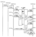
図4は、データ書込時の排他制御不備の例を示す図である。
Next, an example in which two or more data writings collide due to inadequate exclusive control and a flow in which the CPUs 111 to 114 determine such incomplete exclusive control will be described.
FIG. 4 is a diagram showing an example of incomplete control during data writing.

プログラムA,B,C,Dの4つを考える。例えば、プログラムA,Bはユーザプログラムであり、プログラムCはOSプログラムである。プログラムA,B,CはCPU111で実行され、プログラムDはCPU112で実行される。プログラムAは、呼出命令によってプログラムBを呼び出す。これにより、実行中のプログラムがプログラムAからプログラムBに切り替わる。プログラムBは、スーパーバイザコール命令(SVC命令)によってプログラムCを呼び出す。これにより、CPU111の動作モードが変更され、実行中のプログラムがプログラムBからプログラムCに切り替わる(ST10)。   Consider four programs A, B, C, and D. For example, programs A and B are user programs, and program C is an OS program. The programs A, B, and C are executed by the CPU 111, and the program D is executed by the CPU 112. Program A calls program B by a call instruction. As a result, the program being executed is switched from program A to program B. Program B calls program C with a supervisor call instruction (SVC instruction). As a result, the operation mode of CPU 111 is changed, and the program being executed is switched from program B to program C (ST10).

その後に、プログラムC,DがRAM115のブロック#2にユーザデータを書き込む場合を考える。排他制御が正常に行われるとき、プログラムCは、テストアンドセット命令(TS命令)によって、RAM115のブロック#1に記憶されたロックワードを更新する。ロックワードは、RAM115上の領域のロックが獲得されているか否かを示すフラグの集合である。ブロック#2に対応するフラグをOFFからONに更新することで、プログラムCはブロック#2のロックを獲得したことになる(ST11)。   Then, consider a case where programs C and D write user data in block # 2 of RAM 115. When the exclusive control is normally performed, the program C updates the lock word stored in the block # 1 of the RAM 115 by a test and set instruction (TS instruction). The lock word is a set of flags indicating whether or not the lock on the area on the RAM 115 has been acquired. By updating the flag corresponding to the block # 2 from OFF to ON, the program C has acquired the lock of the block # 2 (ST11).

プログラムDがTS命令によってブロック#2のロックを獲得しようとしたとき、プログラムCによって既にロックが獲得されていれば(フラグがONになっていれば)、プログラムDのTS命令は失敗する(ST12)。そして、プログラムDは、継続的に(例えば、定期的に)ブロック#1に記憶されたロックワードを確認し、ブロック#2のロックが解放されるまで(ブロック#2に対応するフラグがOFFになるまで)待つことになる。このような排他制御の方法は、スピンロックと呼ばれることがある。   When the program D tries to acquire the lock of the block # 2 by the TS instruction, if the lock has already been acquired by the program C (if the flag is ON), the TS instruction of the program D fails (ST12). ). Then, the program D continuously checks the lock word stored in the block # 1 (for example, periodically) until the lock of the block # 2 is released (the flag corresponding to the block # 2 is turned OFF). I will wait). Such a method of exclusive control is sometimes called spin lock.

ブロック#2のロックを獲得したプログラムCは、ストア命令(STR命令)によってブロック#2にデータを書き込む(ST13)。データ書込が成功すると、プログラムCは、STR命令によってブロック#1に記憶されたロックワードを更新する。ブロック#2に対応するフラグをONからOFFに更新することで、プログラムCはブロック#2のロックを解放したことになる(ST14)。   The program C that has acquired the lock of the block # 2 writes data to the block # 2 by a store instruction (STR instruction) (ST13). When the data writing is successful, the program C updates the lock word stored in the block # 1 by the STR instruction. By updating the flag corresponding to the block # 2 from ON to OFF, the program C has released the lock of the block # 2 (ST14).

ブロック#2のロックが解放されると、プログラムDは、TS命令によってブロック#1に記憶されたロックワードを更新し、ブロック#2のロックを獲得する(ST15)。ブロック#2のロックを獲得したプログラムDは、プログラムCの場合と同様に、ブロック#2にデータを書き込む(ST16)。ブロック#2へのデータ書込が成功すると、プログラムDは、STR命令によってブロック#1に記憶されたロックワードを更新し、ブロック#2のロックを解放する(ST17)。同一の領域に対するデータ書込が連続しても、排他制御が正常に行われる限り、それらデータ書込は正常であると言える。   When the lock of the block # 2 is released, the program D updates the lock word stored in the block # 1 by the TS instruction, and acquires the lock of the block # 2 (ST15). The program D that acquired the lock of the block # 2 writes data in the block # 2 as in the case of the program C (ST16). When the data writing to the block # 2 is successful, the program D updates the lock word stored in the block # 1 by the STR instruction and releases the lock of the block # 2 (ST17). Even if data writing to the same area continues, it can be said that the data writing is normal as long as the exclusive control is normally performed.

その後に、プログラムC,DがRAM115のブロック#3にデータを書き込む場合を考える。排他制御が正常に行われないとき、プログラムCは、ブロック#3のロックを獲得せずに(ブロック#3に対応するフラグをONにせずに)、STR命令によってブロック#3にデータを書き込む(ST18)。また、プログラムDも、ブロック#3にデータを書き込む(ST19)。排他制御なしにプログラムCによるデータ書込とプログラムDによるデータ書込とが短い時間内に行われた場合、このデータ書込の衝突によって、プログラムCのデータが意図せず破壊されることになり得る。その結果、プログラムCの処理が異常停止するなどの不具合が発生する可能性がある。   Then, consider a case where the programs C and D write data in block # 3 of the RAM 115. When the exclusive control is not normally performed, the program C does not acquire the lock of the block # 3 (without turning on the flag corresponding to the block # 3), and writes data to the block # 3 by the STR instruction ( ST18). Program D also writes data to block # 3 (ST19). If the data writing by the program C and the data writing by the program D are performed within a short time without exclusive control, the data of the program C is unintentionally destroyed due to the collision of the data writing. obtain. As a result, there is a possibility that problems such as abnormal stop of processing of the program C may occur.

図5は、データ書込時の排他制御不備の検出例を示すシーケンス図である。
ここでは、CPU111がCPU112との間でデータ書込が衝突していないか確認する場合を考える。実装時はCPU111は、CPU112と同様に他CPU(CPU113,114)との間でも、データ書込が衝突していないか確認する。また、CPU111以外のCPUも、CPU111と同様にデータ書込が衝突していないか確認する。
FIG. 5 is a sequence diagram illustrating an example of detection of inadequate exclusive control during data writing.
Here, consider a case where the CPU 111 confirms whether data writing has collided with the CPU 112. At the time of mounting, the CPU 111 checks whether data writing has collided with other CPUs (CPUs 113 and 114) as with the CPU 112. Further, CPUs other than the CPU 111 also check whether data writing has collided in the same manner as the CPU 111.

RAM115には、各CPUに対応する制御領域が用意される。CPU111用の制御領域には、CPU111がデータを書き込んだ領域を示すアドレス情報やCPU112〜114から収集したアドレス情報が格納される。また、CPU111用の制御領域には、アドレス情報の収集をCPU112〜114に依頼するか否かを示す依頼フラグが格納される。CPU112用の制御領域にも、同様の情報が格納される。   In the RAM 115, a control area corresponding to each CPU is prepared. In the control area for the CPU 111, address information indicating an area where the CPU 111 has written data and address information collected from the CPUs 112 to 114 are stored. In the control area for the CPU 111, a request flag indicating whether to request the CPUs 112 to 114 to collect address information is stored. Similar information is also stored in the control area for the CPU 112.

CPU111は、以下の制御を開始するとき、CPU111用の制御領域に格納された依頼フラグをONにする(ST20)。命令エミュレータを用いてCPU111でSTR命令が実行されるとき、CPU111は、アクセス先の領域を示すアドレス情報を生成して、CPU111用の制御領域に格納する(ST21)。また、命令エミュレータを用いてCPU112でSTR命令が実行されるとき、CPU112は、アクセス先の領域を示すアドレス情報を生成して、CPU112用の制御領域に格納する(ST22)。このとき、CPU112は、CPU111の依頼フラグを確認し、依頼フラグがONであるときは、生成したアドレス情報をCPU111用の制御領域にコピーする(ST23)。   When starting the following control, the CPU 111 turns on the request flag stored in the control area for the CPU 111 (ST20). When the STR instruction is executed by the CPU 111 using the instruction emulator, the CPU 111 generates address information indicating the access destination area and stores it in the control area for the CPU 111 (ST21). Further, when the STR instruction is executed by the CPU 112 using the instruction emulator, the CPU 112 generates address information indicating the access destination area and stores it in the control area for the CPU 112 (ST22). At this time, the CPU 112 checks the request flag of the CPU 111, and when the request flag is ON, copies the generated address information to the control area for the CPU 111 (ST23).

同様にして、CPU111は、CPU111でSTR命令が実行されるとき、アドレス情報を生成してCPU111用の制御領域に格納する(ST24)。CPU112は、CPU112でSTR命令が実行されるとき、アドレス情報を生成してCPU112用の制御領域に格納する(ST25)。また、CPU112は、依頼フラグがONであることを確認し、アドレス情報をCPU111用の制御領域にコピーする(ST26)。   Similarly, when the CPU 111 executes the STR instruction, the CPU 111 generates address information and stores it in the control area for the CPU 111 (ST24). When the STR instruction is executed by the CPU 112, the CPU 112 generates address information and stores it in the control area for the CPU 112 (ST25). Further, the CPU 112 confirms that the request flag is ON, and copies the address information to the control area for the CPU 111 (ST26).

後述する所定の条件が満たされると、CPU111は、CPU111用の制御領域に格納された依頼フラグをOFFにし、CPU112からのアドレス情報の収集を停止する。そして、CPU111は、CPU111用の制御領域に収集されているアドレス情報を用いて、直近の1区間内でCPU111とCPU112とが同一または近い領域に対してデータ書込を行ったか(データ書込の衝突があったか)確認する。すなわち、CPU111は、CPU111のアドレス情報が示すアドレスとCPU112のアドレス情報が示すアドレスとが、重複または近接しているか確認する(ST27)。   When a predetermined condition described later is satisfied, the CPU 111 turns off the request flag stored in the control area for the CPU 111 and stops collecting address information from the CPU 112. Then, the CPU 111 uses the address information collected in the control area for the CPU 111 to determine whether the CPU 111 and the CPU 112 have performed data writing in the same or close area within the latest one section (data writing). Check if there was a collision. That is, CPU 111 checks whether the address indicated by the address information of CPU 111 and the address indicated by the address information of CPU 112 overlap or are close to each other (ST27).

データ書込の衝突が検出された場合、CPU111は、CPU111で実行中のプログラムおよびCPU112で実行中のプログラムの少なくとも一方に排他制御の不備があると判定する。一方、データ書込の衝突が検出されない場合、CPU111は、直近の1区間内で実行された命令については排他制御の不備がないと判定する。図5の排他制御不備なしの例では、直近の1区間について排他制御の不備がないと判定している。なお、直近の1区間とは、依頼フラグを前回ONにしてから、依頼フラグをOFFにするまで(後述する所定の条件が満たされるまで)の区間である。CPU111は、排他制御の不備の有無を判定した後は、収集したアドレス情報を破棄してよい。   When a data write collision is detected, the CPU 111 determines that at least one of the program being executed by the CPU 111 and the program being executed by the CPU 112 is deficient in exclusive control. On the other hand, when a data write collision is not detected, the CPU 111 determines that there is no deficiency in exclusive control for an instruction executed in the latest one section. In the example of no exclusive control deficiency in FIG. 5, it is determined that there is no deficiency in exclusive control for the latest one section. The most recent section is a section from when the request flag is turned on last time until the request flag is turned off (until a predetermined condition described later is satisfied). The CPU 111 may discard the collected address information after determining whether or not the exclusive control is deficient.

その後、CPU111は、CPU111用の制御領域に格納された依頼フラグをONにし、CPU112からのアドレス情報の収集を再開する(ST28)。ステップST21〜ST26と同様に、CPU111は、アドレス情報を適宜生成してCPU111用の制御領域に格納する。また、CPU112は、アドレス情報を適宜生成してCPU112用の制御領域に格納すると共に、CPU111用の制御領域にコピーする。   Thereafter, the CPU 111 turns on the request flag stored in the control area for the CPU 111, and resumes collection of address information from the CPU 112 (ST28). As in steps ST21 to ST26, the CPU 111 generates address information as appropriate and stores it in the control area for the CPU 111. Further, the CPU 112 generates address information as appropriate and stores it in the control area for the CPU 112, and copies it to the control area for the CPU 111.

所定の条件が満たされると、CPU111は、CPU111用の制御領域に格納された依頼フラグをOFFにし、PU112からのアドレス情報の収集を停止する。そして、CPU111は、CPU111用の制御領域に収集されているアドレス情報を用いて、排他制御の不備の有無を判定する。図5の排他制御不備ありの例では、ここで排他制御の不備があると判定している(ST29)。排他制御の不備があると判定した場合、CPU111は、CPU111,112で実行されていたプログラムを特定するためのプログラム情報などを含むログ情報を生成し、ログファイルとしてHDD121に出力する。   When a predetermined condition is satisfied, the CPU 111 turns off the request flag stored in the control area for the CPU 111 and stops collecting address information from the PU 112. Then, the CPU 111 determines whether or not the exclusive control is deficient by using the address information collected in the control area for the CPU 111. In the example of lack of exclusive control in FIG. 5, it is determined here that there is a lack of exclusive control (ST29). If it is determined that there is a lack of exclusive control, the CPU 111 generates log information including program information for specifying the program executed by the CPUs 111 and 112 and outputs the log information to the HDD 121 as a log file.

このように、CPU111は、1つの区間内で収集されたアドレス情報同士を比較することで、排他制御の不備を判定する。排他制御の不備を判定するタイミング、すなわち、区間を区切るタイミングは、次の6つの条件の何れかが満たされたときとする。   As described above, the CPU 111 determines deficiencies in exclusive control by comparing the address information collected in one section. The timing for determining the deficiency of exclusive control, that is, the timing for dividing the section is when any of the following six conditions is satisfied.

第1の条件は、他のユーザプログラムの呼び出し、呼び出したユーザプログラムからの復帰、タイマ割り込みなどによってユーザプログラム間の切替が発生したことである。第2の条件は、SVC命令などによってユーザプログラムとシステムプログラム間の切替が発生したことである。第1および第2の条件に応じて区間を区切ることで、排他制御の不備があるプログラムの範囲が限定できるので、不備の特定が容易になる。第3の条件は、RAM115の領域に対してロックが獲得されたことである。第4の条件は、ロックが解放されたことである。第3および第4の条件に応じて区間を区切ることで、正常な排他制御のもとで行われるデータ書込が排他制御の不備であると誤判定されるのを抑制できる。   The first condition is that switching between user programs has occurred due to a call to another user program, a return from the called user program, a timer interrupt, or the like. The second condition is that switching between the user program and the system program has occurred due to an SVC instruction or the like. By delimiting the sections according to the first and second conditions, the range of programs having incomplete control can be limited, so that it is easy to identify the incompleteness. The third condition is that a lock has been acquired for the RAM 115 area. The fourth condition is that the lock has been released. By dividing the section according to the third and fourth conditions, it is possible to suppress erroneous determination that data writing performed under normal exclusive control is deficient in exclusive control.

第5の条件は、実行中のプログラムの動作モードの切り替えが発生したことである。動作モードには、入出力装置からの割り込みやタイマ割り込みを禁止するモードと禁止しないモードとがある。第6の条件は、排他制御の不備が前回判定されてから(依頼フラグがONになってから)、所定数の命令が実行されたことである。   The fifth condition is that the operation mode of the program being executed has been switched. The operation mode includes a mode for prohibiting an interrupt from the input / output device and a timer interrupt and a mode for prohibiting the interrupt. The sixth condition is that a predetermined number of instructions have been executed since the failure of exclusive control was determined last time (after the request flag was turned ON).

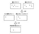
図6は、排他制御不備の有無の判定例を示す図である。
排他制御の不備を判定するにあたり、第2の実施の形態では、RAM115の各ブロックに対するデータ書込の有無を示す書込ビットマップが用いられる。書込ビットマップでは、直近の区間においてデータ書込があったブロック(ブロックについては、後述する図14に関する説明を参照)に対応するビットが1に設定され、データ書込がなかったブロックに対応するビットが0に設定されている。
FIG. 6 is a diagram illustrating an example of determining whether there is a lack of exclusive control.
In determining the lack of exclusive control, in the second embodiment, a write bit map indicating whether or not data is written to each block of the RAM 115 is used. In the write bit map, the bit corresponding to the block in which data was written in the most recent section (for the block, see the description related to FIG. 14 described later) is set to 1 and corresponds to the block in which no data was written The bit to be set is set to 0.

CPU111は、CPU111で生成された書込ビットマップとCPU112で生成された書込ビットマップの論理積(AND)を求める。論理積としてのビットマップでは、CPU111,112の両方からデータ書込のあったブロックに対応するビットが1になり、それ以外のブロックに対応するビットが0になる。論理積の全ビットが0であれば、CPU111,112は同じブロックに対してデータ書込を行っていないことになる。   The CPU 111 calculates a logical product (AND) of the write bitmap generated by the CPU 111 and the write bitmap generated by the CPU 112. In the bit map as the logical product, the bit corresponding to the block in which the data has been written from both the CPUs 111 and 112 becomes 1, and the bits corresponding to the other blocks become 0. If all the bits of the logical product are 0, the CPUs 111 and 112 have not written data to the same block.

ただし、論理積としてのビットマップの中に1のビットがあっても、そのビットに対応するブロックはロックワードが記憶されているブロックである可能性がある。CPU111,112の両方がロックワードを更新することは正常な排他制御であるため、ロックワードへのアクセスを除外して排他制御の不備を判定することが好ましい。   However, even if there is one bit in the bit map as the logical product, there is a possibility that the block corresponding to that bit is a block in which the lock word is stored. Since it is normal exclusive control that both the CPUs 111 and 112 update the lock word, it is preferable to determine the lack of exclusive control by excluding access to the lock word.

そこで、CPU111は、ロック獲得命令としてのTS命令によってアクセスされたブロックを示す書込ビットマップを生成する。CPU111は、上記の論理積としてのビットマップと排他制御用の書込ビットマップの排他的論理和(XOR)を求める。排他的論理和としてのビットマップでは、ロックワードでないデータがCPU111,112の両方から書き込まれたブロックに対応するビットが1になり、それ以外のブロックに対応するビットが0になる。論理積としてのビットマップの中に1のビットがあっても、排他的論理和の全ビットが0であれば、CPU111,112は排他制御の不備に該当するような同一ブロックへのデータ書込を行っていないことになる。   Therefore, the CPU 111 generates a write bit map indicating the block accessed by the TS instruction as the lock acquisition instruction. The CPU 111 obtains an exclusive OR (XOR) of the bitmap as the logical product and the write bitmap for exclusive control. In the bit map as the exclusive OR, the bit corresponding to the block in which the data that is not the lock word is written from both of the CPUs 111 and 112 becomes 1, and the bits corresponding to the other blocks become 0. Even if there is 1 bit in the bit map as the logical product, if all the bits of the exclusive logical sum are 0, the CPUs 111 and 112 write data to the same block corresponding to the lack of exclusive control. Will not go.

以上では、同一ブロックに対するデータ書込の有無を確認したが、CPU111は、同様にして近接するブロックに対するデータ書込の有無についても確認する。例えば、CPU111は、CPU111の書込ビットマップで1に設定されているビットの前後所定数のビットも1に書き換えて、CPU112の書込ビットマップとの論理積を求める。この論理積としてのビットマップの中に1のビットがある場合、CPU111は、この論理積としてのビットマップと排他制御用の書込ビットマップとの排他的論理和を求める。   In the above, the presence / absence of data writing to the same block has been confirmed, but the CPU 111 similarly confirms the presence / absence of data writing to adjacent blocks. For example, the CPU 111 rewrites a predetermined number of bits before and after the bit set to 1 in the write bitmap of the CPU 111 to 1 and obtains a logical product with the write bitmap of the CPU 112. When there is 1 bit in the bit map as the logical product, the CPU 111 obtains an exclusive logical sum of the bit map as the logical product and the write bitmap for exclusive control.

このようにして、書換前のCPU111の書込ビットマップを用いた論理積または排他的論理和の全ビットが0になれば、同一ブロックに対する実質的なデータ書込の衝突がないと判断できる。また、書換後のCPU111の書込ビットマップを用いた論理積または排他的論理和の全ビットが0になれば、近接するブロックに対する実質的なデータ書込の衝突がないと判断できる。CPU111は、同一または近接するブロックに対する実質的なデータ書込の衝突がなければ、直近の区間について排他制御の不備がないと判定する。一方、CPU111は、それ以外の場合は排他制御の不備があると判定する。   In this way, if all the bits of the logical product or exclusive logical sum using the write bitmap of the CPU 111 before rewriting become 0, it can be determined that there is no substantial data write collision for the same block. Further, if all the bits of the logical product or exclusive logical sum using the write bitmap of the CPU 111 after rewriting become 0, it can be determined that there is no substantial data write collision with adjacent blocks. If there is no substantial data writing collision with the same or adjacent blocks, the CPU 111 determines that there is no deficiency in exclusive control for the most recent section. On the other hand, the CPU 111 determines that there is a lack of exclusive control otherwise.

次に、情報処理装置100の機能およびデータ構造について説明する。
図7は、情報処理装置の機能例を示すブロック図である。
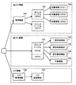
情報処理装置100は、命令判別部131、命令変換部132、制御情報記憶部133、ログファイル記憶部134、起動部135およびデバッグ支援部136を有する。
Next, functions and data structures of the information processing apparatus 100 will be described.
FIG. 7 is a block diagram illustrating an example of functions of the information processing apparatus.
The information processing apparatus 100 includes an instruction determination unit 131, an instruction conversion unit 132, a control information storage unit 133, a log file storage unit 134, an activation unit 135, and a debug support unit 136.

命令判別部131、命令変換部132、起動部135およびデバッグ支援部136は、命令エミュレータの中のソフトウェアモジュールとして実現できる。命令判別部131、命令変換部132およびデバッグ支援部136の処理は、複数のCPU(CPU111〜114)で並列に実行される。ここでは主に、命令判別部131、命令変換部132、起動部135およびデバッグ支援部136がCPU111で動作する場合を説明する。制御情報記憶部133は、RAM115に確保した領域として実現できる。ログファイル記憶部134は、HDD121に確保した記憶領域として実現できる。   The instruction determination unit 131, the instruction conversion unit 132, the activation unit 135, and the debug support unit 136 can be realized as software modules in the instruction emulator. The processes of the instruction determination unit 131, the instruction conversion unit 132, and the debug support unit 136 are executed in parallel by a plurality of CPUs (CPUs 111 to 114). Here, a case will be mainly described in which the instruction determination unit 131, the instruction conversion unit 132, the activation unit 135, and the debug support unit 136 operate on the CPU 111. The control information storage unit 133 can be realized as an area secured in the RAM 115. The log file storage unit 134 can be realized as a storage area secured in the HDD 121.

命令判別部131は、命令(例えば、システムプログラムの命令)が読み込まれると、読み込まれた命令の種類を判別する。命令の種類が所定の種類である場合、命令判別部131は、命令を命令変換部132とデバッグ支援部136の両方に渡す。命令の種類が所定の種類でない場合、命令判別部131は、命令を命令変換部132に渡す。第2の実施の形態では、所定の種類の命令として主に、データの書込またはロック解放に用いるSTR命令、ロック獲得に用いるTS命令、ユーザプログラムの呼出に用いる呼出命令、および、システムプログラムの呼出に用いるSVC命令の4種類を考える。   When an instruction (for example, a system program instruction) is read, the instruction determination unit 131 determines the type of the read instruction. When the instruction type is a predetermined type, the instruction determination unit 131 passes the instruction to both the instruction conversion unit 132 and the debug support unit 136. If the instruction type is not a predetermined type, the instruction determination unit 131 passes the instruction to the instruction conversion unit 132. In the second embodiment, as a predetermined type of instruction, a STR instruction used for data writing or lock release, a TS instruction used for lock acquisition, a call instruction used for calling a user program, and a system program Consider four types of SVC instructions used for calls.

命令変換部132は、命令判別部131から渡された命令をCPU111が解釈可能な命令に変換し、CPU111に実行させる。命令の実行が完了すると、命令変換部132は、命令の実行結果をデバッグ支援部136に通知する。例えば、命令変換部132は、TS命令が実行されたときにはロック獲得の成否をデバッグ支援部136に通知する。   The instruction conversion unit 132 converts the instruction passed from the instruction determination unit 131 into an instruction interpretable by the CPU 111 and causes the CPU 111 to execute the instruction. When the execution of the instruction is completed, the instruction conversion unit 132 notifies the debug support unit 136 of the execution result of the instruction. For example, the instruction conversion unit 132 notifies the debug support unit 136 of the success or failure of the lock acquisition when the TS instruction is executed.

制御情報記憶部133は、排他制御の不備の判定に用いられる制御情報を記憶する。制御情報記憶部133の領域は、デバッグ支援部136が起動するときに起動部135によってRAM115上に確保される。制御情報記憶部133は、CPU111〜114から共通にアクセス可能である。ただし、アドレス情報やプログラム情報を収集する領域については、制御情報記憶部133内にCPU毎に区分して設けられている。   The control information storage unit 133 stores control information used for determining whether or not exclusive control is defective. The area of the control information storage unit 133 is secured on the RAM 115 by the activation unit 135 when the debug support unit 136 is activated. The control information storage unit 133 can be commonly accessed from the CPUs 111 to 114. However, areas for collecting address information and program information are provided in the control information storage unit 133 for each CPU.

ログファイル記憶部134は、ログファイルを記憶する。ログファイルには、排他制御の不備に該当するデータ書込の衝突が検出されたときに、問題となったデータ書込についての情報(アドレス情報やプログラム情報など)がログ情報として書き込まれる。情報処理装置100のユーザは、デバッグ作業において、ログファイルに記載されたログ情報を分析することで、排他制御の不備のあるプログラムを特定することが容易となり、不具合が発生しないようにプログラムを修正することが容易となる。   The log file storage unit 134 stores a log file. In the log file, information (address information, program information, etc.) about the data write that has become a problem when a data write collision corresponding to the lack of exclusive control is detected is written as log information. The user of the information processing apparatus 100 can easily identify a program that lacks exclusive control by analyzing the log information described in the log file during debugging, and corrects the program so that no malfunction occurs. Easy to do.

起動部135は、ユーザからデバッグ開始のコマンドやデバッグ終了のコマンドを受け付ける。デバッグ開始のコマンドが入力されると、起動部135は、RAM115に制御情報記憶部133の領域を確保し、デバッグ支援部136を起動して排他制御の不備を判定できるようにする。デバッグ終了のコマンドが入力されると、起動部135は、デバッグ支援部136を停止させ、制御情報記憶部133の領域を解放する。   The activation unit 135 receives a debug start command and a debug end command from the user. When a command to start debugging is input, the activation unit 135 secures an area for the control information storage unit 133 in the RAM 115 and activates the debug support unit 136 so as to determine the lack of exclusive control. When a debug end command is input, the activation unit 135 stops the debug support unit 136 and releases the area of the control information storage unit 133.

デバッグ支援部136は、命令判別部131によって読み込まれる命令を監視し、CPU111〜114で実行されるプログラムの排他制御の不備を判定する。デバッグ支援部136は、情報収集部137、情報提供部138および検出部139を有する。   The debug support unit 136 monitors instructions read by the instruction determination unit 131 and determines deficiencies in exclusive control of programs executed by the CPUs 111 to 114. The debug support unit 136 includes an information collection unit 137, an information provision unit 138, and a detection unit 139.

情報収集部137は、CPU111が排他制御の不備の判定に用いる情報を収集する。情報収集部137は、CPU111でSTR命令が実行されるとき、当該STR命令に関するアドレス情報やプログラム情報などを生成して制御情報記憶部133に格納する。また、情報収集部137は、CPU111でTS命令が実行されるとき、当該TS命令に関するアドレス情報などを生成して制御情報記憶部133に格納する。また、情報収集部137は、CPU111の依頼フラグをONにすることで、CPU112〜114からSTR命令に関するアドレス情報やプログラム情報などを収集する。   The information collection unit 137 collects information used by the CPU 111 to determine whether the exclusive control is defective. When the CPU 111 executes the STR instruction, the information collection unit 137 generates address information, program information, and the like related to the STR instruction and stores them in the control information storage unit 133. In addition, when the CPU 111 executes a TS command, the information collection unit 137 generates address information and the like related to the TS command and stores them in the control information storage unit 133. The information collection unit 137 collects address information, program information, and the like regarding the STR command from the CPUs 112 to 114 by turning on the request flag of the CPU 111.

情報提供部138は、CPU112〜114が排他制御の不備の判定に用いる情報を、CPU112〜114に提供する。情報提供部138は、CPU111でSTR命令が実行されるとき、CPU112〜114の依頼フラグを確認する。依頼フラグがONであれば、情報提供部138は、情報収集部137が生成した当該STR命令に関するアドレス情報やプログラム情報などをCPU112〜114に提供する。具体的には、情報提供部138は、生成されたアドレス情報やプログラム情報などを、制御情報記憶部133の中のCPU112〜114に対応する領域にコピーする。   The information providing unit 138 provides the CPUs 112 to 114 with information used by the CPUs 112 to 114 for determining whether the exclusive control is defective. The information providing unit 138 checks the request flags of the CPUs 112 to 114 when the CPU 111 executes the STR command. If the request flag is ON, the information providing unit 138 provides the CPU 112 to 114 with address information, program information, and the like regarding the STR command generated by the information collecting unit 137. Specifically, the information providing unit 138 copies the generated address information, program information, and the like to an area corresponding to the CPUs 112 to 114 in the control information storage unit 133.

検出部139は、前述のような所定の条件が満たされたタイミングで、制御情報記憶部133の中のCPU111に対応する領域に収集された情報を用いて、排他制御の不備を判定する。所定の条件は、例えば、CPU111で呼出命令またはSVC命令などが実行されてプログラムの切り替えが発生すること、TS命令によりロック獲得が成功したこと、ロックが解放されること、または、前回判定を行ってからCPU111で所定数の命令が実行されたことである。   The detection unit 139 determines deficiency of exclusive control using information collected in an area corresponding to the CPU 111 in the control information storage unit 133 at a timing when the predetermined condition as described above is satisfied. The predetermined condition is, for example, that the CPU 111 executes a call instruction or SVC instruction or the like to switch programs, that the TS instruction has successfully acquired the lock, that the lock is released, or that the previous determination is performed. The CPU 111 has executed a predetermined number of instructions since then.

なお、情報収集部137は、命令の実行が完了する前に当該命令に関する情報を生成してもよいし、命令の実行が完了してから当該命令に関する情報を生成してもよい。生成された情報を情報提供部138がコピーするタイミングについても同様である。また、検出部139は、呼出命令、SVC命令またはロック解放を示すSTR命令に応じて排他制御の不備を判定するときは、その命令の実行が完了する前に判定を開始してもよいし、命令の実行が完了してから判定を開始してもよい。また、検出部139は、命令実行数に応じて排他制御の不備を判定するときは、最後の命令の実行が完了する前に判定を開始してもよいし、最後の命令の実行が完了してから判定を開始してもよい。   Note that the information collection unit 137 may generate information regarding the instruction before the execution of the instruction is completed, or may generate information regarding the instruction after the execution of the instruction is completed. The same applies to the timing at which the information providing unit 138 copies the generated information. In addition, when the detection unit 139 determines the lack of exclusive control according to the call instruction, the SVC instruction, or the STR instruction indicating the lock release, the detection unit 139 may start the determination before the execution of the instruction is completed, The determination may be started after execution of the instruction is completed. In addition, when the detection unit 139 determines the lack of exclusive control according to the number of executed instructions, the detection unit 139 may start the determination before the execution of the last instruction is completed, or the execution of the last instruction is completed. The determination may be started after that.

図8は、第2の実施の形態の制御情報の全体構造例を示す図である。
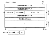
制御情報記憶部133には、図8に示すような構造をもつ制御情報が格納される。制御情報は、他CPU情報を管理するために、管理情報141、ポインタテーブル142を含む複数の第1のポインタテーブル、および、収集領域143を含む複数の収集領域を有する。また、制御情報は、自CPU情報を管理するために、ポインタテーブル151(第2のポインタテーブル)、一般記録領域152を含む複数の一般記録領域、排他記録領域153を含む複数の排他記録領域、排他管理情報154を含む複数の排他管理情報、および、作業領域155を含む複数の作業域を有する。また、制御情報は、ログ情報を管理するために、ログ管理情報156およびログ記録領域157を有する。
FIG. 8 is a diagram illustrating an example of the overall structure of the control information according to the second embodiment.
The control information storage unit 133 stores control information having a structure as shown in FIG. The control information includes management information 141, a plurality of first pointer tables including a pointer table 142, and a plurality of collection areas including a collection area 143 in order to manage other CPU information. The control information includes a pointer table 151 (second pointer table), a plurality of general recording areas including a general recording area 152, a plurality of exclusive recording areas including an exclusive recording area 153, in order to manage the own CPU information. It has a plurality of exclusion management information including exclusion management information 154 and a plurality of work areas including a work area 155. The control information includes log management information 156 and a log recording area 157 for managing log information.

管理情報141は、情報処理装置100全体の状態やCPU111〜114それぞれの状態を示す。第1のポインタテーブルは、CPU111〜114に対応して設けられる。1つの第1のポインタテーブルは、1つの「自CPU」を示す。管理情報141から第1のポインタテーブルを辿ることができる。収集領域には、他CPUから収集された情報が格納される。収集領域は、「自CPU」と「他CPU」の組み合わせ毎に設けられる。1つの「自CPU」に対応する第1のポインタテーブルから、「他CPU」に対応する3つの収集領域を辿ることができる。例えば、CPU111に対応する第1のポインタテーブルから、CPU112〜114に対応する収集領域を辿ることができる。   The management information 141 indicates the state of the entire information processing apparatus 100 and the states of the CPUs 111 to 114. The first pointer table is provided corresponding to the CPUs 111 to 114. One first pointer table indicates one “own CPU”. The first pointer table can be traced from the management information 141. Information collected from other CPUs is stored in the collection area. The collection area is provided for each combination of “own CPU” and “other CPU”. Three collection areas corresponding to “other CPUs” can be traced from the first pointer table corresponding to one “own CPU”. For example, the collection area corresponding to the CPUs 112 to 114 can be traced from the first pointer table corresponding to the CPU 111.

ポインタテーブル151は、CPU111〜114それぞれのロック獲得状況を示す情報を含む。一般記録領域には、自CPUで実行されるSTR命令に関するアドレス情報やプログラム情報などが格納される。排他記録領域には、自CPUで実行されるTS命令に関するアドレス情報などが格納される。排他管理情報は、ロック獲得時に更新されたロックワードのアドレスを含む。ロックワードのアドレスは、STR命令がロック解放を示すものであるか判断するために用いられる。作業領域は、自CPUで生成された情報を一時的に記憶する。一般記録領域、排他記録領域、排他管理情報および作業領域は、CPU111〜114に対応して設けられ、ポインタテーブル151から辿ることができる。   The pointer table 151 includes information indicating the lock acquisition status of each of the CPUs 111 to 114. The general recording area stores address information, program information, and the like related to the STR instruction executed by the CPU. In the exclusive recording area, address information related to a TS command executed by the CPU is stored. The exclusive management information includes the address of the lock word updated when the lock is acquired. The address of the lock word is used to determine whether the STR instruction indicates a lock release. The work area temporarily stores information generated by its own CPU. The general recording area, exclusive recording area, exclusive management information, and work area are provided corresponding to the CPUs 111 to 114 and can be traced from the pointer table 151.

ログ管理情報156は、ログ記録領域157を管理するための情報を含む。ログ記録領域157には、排他制御の不備があると判定されたときに、検出部139によって生成されたログ情報が格納される。ログ記録領域157に格納されたログ情報は、ログファイル記憶部134に記憶された(HDD121上の)ログファイルに書き出される。   The log management information 156 includes information for managing the log recording area 157. The log recording area 157 stores log information generated by the detection unit 139 when it is determined that there is a lack of exclusive control. The log information stored in the log recording area 157 is written to a log file (on the HDD 121) stored in the log file storage unit 134.

図9は、第2の実施の形態の管理情報のデータ構造例を示す図である。
管理情報141は、ヘッダ内に、システム状態、ロックワードおよび対象プログラムの項目を有する。また、管理情報141は、CPU111〜114それぞれについて、CPU状態およびポインタテーブルのアドレスの項目を有する。
FIG. 9 illustrates an example data structure of management information according to the second embodiment.
The management information 141 has items of system status, lock word, and target program in the header. Further, the management information 141 includes items of CPU status and pointer table address for each of the CPUs 111 to 114.

システム状態の項目は、デバッグ開始フラグを含む。デバッグ開始フラグは、デバッグ支援部136が動作中であるか否かを示す。デバッグ開始フラグは、1ビットで表現できる。例えば、デバッグ開始フラグ=1(ON)は、デバッグ支援部136が動作中であり排他制御の不備が判定されることを示す。デバッグ開始フラグ=0(OFF)は、デバッグ支援部136が停止中であり排他制御の不備が判定されないことを示す。ロックワードの項目は、管理情報141へのアクセスの排他制御に用いられるロックワードを含む。対象プログラムの項目は、デバッグ対象のプログラム(排他制御の不備を判定するプログラム)の識別情報を含む。対象プログラムは、例えば、ユーザが指定することもできる。対象プログラムを限定することで、情報処理装置100の負荷を軽減できる。   The item of system state includes a debug start flag. The debug start flag indicates whether or not the debug support unit 136 is operating. The debug start flag can be expressed by 1 bit. For example, the debug start flag = 1 (ON) indicates that the debug support unit 136 is operating and it is determined that the exclusive control is defective. The debug start flag = 0 (OFF) indicates that the debug support unit 136 is stopped and the lack of exclusive control is not determined. The item of the lock word includes a lock word used for exclusive control of access to the management information 141. The item of the target program includes identification information of a program to be debugged (a program for determining deficiencies in exclusive control). The target program can also be specified by the user, for example. By limiting the target program, the load on the information processing apparatus 100 can be reduced.

CPU状態の項目は、依頼フラグを含む。依頼フラグは、あるCPUが他CPUに対して情報収集を依頼しているか否かを示す。依頼フラグは、1ビットで表現できる。例えば、依頼フラグ=1(ON)は、情報収集を依頼中であることを示す。依頼フラグ=0(OFF)は、情報収集を依頼していないことを示す。ポインタテーブルのアドレスの項目は、第1のポインタテーブルが存在するRAM115の領域の先頭アドレスである。   The item of CPU status includes a request flag. The request flag indicates whether a certain CPU requests information collection from another CPU. The request flag can be expressed by 1 bit. For example, a request flag = 1 (ON) indicates that information collection is being requested. Request flag = 0 (OFF) indicates that information collection is not requested. The item of the address of the pointer table is the head address of the area of the RAM 115 where the first pointer table exists.

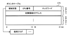
図10は、第1のポインタテーブルのデータ構造例を示す図である。
ポインタテーブル142は、「他CPU」それぞれについて(例えば、CPU112〜114それぞれについて)、領域状態、ロックワードおよび収集領域のアドレスの項目を有する。領域状態の項目は、使用フラグを含む。使用フラグは、収集領域が使用されているか否か、すなわち、他CPUから収集された情報が存在するか否かを示す。使用フラグは、1ビットで表現できる。例えば、使用フラグ=1(ON)は、収集された情報が存在することを示す。使用フラグ=0(OFF)は、収集された情報が存在しないことを示す。ロックワードの項目は、ポインタテーブル142へのアクセスの排他制御に用いられる。収集領域のアドレスの項目は、RAM115上の収集領域の先頭アドレスである。
FIG. 10 is a diagram illustrating a data structure example of the first pointer table.
The pointer table 142 includes items of an area state, a lock word, and a collection area address for each “other CPU” (for example, each of the CPUs 112 to 114). The area state item includes a use flag. The use flag indicates whether or not the collection area is used, that is, whether or not information collected from another CPU exists. The use flag can be expressed by 1 bit. For example, use flag = 1 (ON) indicates that the collected information exists. Use flag = 0 (OFF) indicates that the collected information does not exist. The lock word item is used for exclusive control of access to the pointer table 142. The collection area address item is the start address of the collection area on the RAM 115.

図11は、収集領域のデータ構造例を示す図である。
収集領域143は、収集領域ヘッダ144、集計領域145を含む複数の集計領域、および、追記領域147を含む複数の追記領域を有する。
FIG. 11 is a diagram illustrating an example of the data structure of the collection area.
The collection area 143 includes a collection area header 144, a plurality of aggregation areas including the aggregation area 145, and a plurality of additional recording areas including the additional recording area 147.

収集領域ヘッダ144は、集計領域の集合の状態を示す。各集計領域は、RAM115上のデータ書込が行われたブロックを示す書込ビットマップを含む。1つの集計領域は、RAM115の1つのアドレス範囲に対応する。1つの集計領域が担当するアドレス範囲の大きさは、予め設定されている。排他制御の不備を判定する1つの区間内で、異なるアドレス範囲に属する領域に対してデータ書込が行われた場合、複数の集計領域が使用されることになる。複数の集計領域は、連結リストとして形成されている。収集領域ヘッダ144からは、先頭の集計領域と末尾の集計領域とを辿ることができる。   The collection area header 144 indicates the state of the aggregation area set. Each total area includes a write bit map indicating a block in which data is written on the RAM 115. One total area corresponds to one address range of the RAM 115. The size of the address range handled by one aggregation area is set in advance. When data is written to areas belonging to different address ranges within one section for determining the lack of exclusive control, a plurality of total areas are used. The plurality of total areas are formed as a linked list. From the collection area header 144, it is possible to trace the head total area and the last total area.

1つの集計領域に対して、複数の追記領域が設けられる。各追記領域は、書込ビットマップ以外のアドレス情報やプログラム情報や時刻情報などを含む。1つの追記領域は、1回のデータ書込に対応する。1つの集計領域に対応する複数の追記領域は、連結リストとして形成されている。集計領域からは、先頭の追記領域を辿ることができる。   A plurality of additional write areas are provided for one total area. Each additional recording area includes address information other than the write bitmap, program information, time information, and the like. One additional recording area corresponds to one data writing. A plurality of additional write areas corresponding to one total area are formed as a linked list. From the total area, the head additional area can be traced.

図12は、収集領域ヘッダのデータ構造例を示す図である。
収集領域ヘッダ144は、領域状態、先頭の集計領域のアドレスおよび末尾の集計領域のアドレスの項目を有する。領域状態の項目は、使用フラグを含む。使用フラグは、少なくとも1つの集計領域が使用されているか否かを示す。使用フラグは、1ビットで表現できる。例えば、使用フラグ=1(ON)は、少なくとも1つの集計領域が使用されていることを示す。使用フラグ=0(OFF)は、何れの集計領域も使用されていないことを示す。先頭の集計領域のアドレスの項目は、RAM115上の先頭の集計領域の先頭アドレスである。末尾の集計領域のアドレスの項目は、末尾の集計領域の先頭アドレスである。
FIG. 12 is a diagram illustrating an example of the data structure of the collection area header.
The collection area header 144 includes items of an area state, an address of the first aggregation area, and an address of the last aggregation area. The area state item includes a use flag. The use flag indicates whether or not at least one total area is used. The use flag can be expressed by 1 bit. For example, use flag = 1 (ON) indicates that at least one total area is used. A use flag = 0 (OFF) indicates that no total area is used. The item of the address of the first total area is the start address of the first total area on the RAM 115. The item of the address of the last counting area is the head address of the last counting area.

図13は、集計領域のデータ構造例を示す図である。
集計領域145は、ヘッダ内に、次の集計領域のアドレス、領域状態、書込ビットマップに対応するメモリアドレス、先頭の追記領域のアドレスおよび末尾の追記領域のアドレスの項目を有する。また、集計領域145は、書込ビットマップ146を有する。
FIG. 13 is a diagram illustrating an example of the data structure of the total area.
The total area 145 includes items of the address of the next total area, the area state, the memory address corresponding to the write bitmap, the address of the first additional area, and the address of the last additional area in the header. The total area 145 includes a write bitmap 146.

次の集計領域のアドレスの項目は、RAM115上の次の集計領域の先頭アドレスを含む。領域状態の項目は、末尾フラグおよび使用フラグを含む。末尾フラグは、集計領域145が連結リストの末尾であるか否かを示す。末尾フラグは、1ビットで表現できる。例えば、末尾フラグ=1(ON)は、集計領域145が連結リストの末尾であることを示す。末尾フラグ=0(OFF)は、集計領域145の後方に他の集計領域があることを示す。使用フラグは、集計領域145が使用されているか否かを示す。使用フラグは、1ビットで表現できる。例えば、使用フラグ=1(ON)は、集計領域145が使用中であることを示す。使用フラグ=0(OFF)は、集計領域145が未使用であることを示す。   The next total area address item includes the start address of the next total area on the RAM 115. The area state item includes a tail flag and a use flag. The end flag indicates whether or not the total area 145 is the end of the linked list. The end flag can be expressed by 1 bit. For example, the end flag = 1 (ON) indicates that the aggregation area 145 is the end of the linked list. The tail flag = 0 (OFF) indicates that there is another counting area behind the counting area 145. The use flag indicates whether or not the total area 145 is used. The use flag can be expressed by 1 bit. For example, use flag = 1 (ON) indicates that the total area 145 is in use. Use flag = 0 (OFF) indicates that the total area 145 is unused.

書込ビットマップに対応するメモリアドレスの項目は、書込ビットマップ146が担当するRAM115のアドレス範囲の先頭アドレスを含む。先頭の追記領域のアドレスの項目は、集計領域145に対応するRAM115上の複数の追記領域のうち、先頭の追記領域の先頭アドレスを含む。末尾の追記領域のアドレスの項目は、集計領域145に対応するRAM115上の複数の追記領域のうち、末尾の追記領域の先頭アドレスである。   The item of the memory address corresponding to the write bitmap includes the start address of the address range of the RAM 115 that the write bitmap 146 is responsible for. The item of the address of the first additional recording area includes the first address of the first additional recording area among the plurality of additional recording areas on the RAM 115 corresponding to the total area 145. The item of the address of the tail additional recording area is the head address of the tail additional recording area among the plurality of additional recording areas on the RAM 115 corresponding to the total area 145.

図14は、書込ビットマップのデータ構造例を示す図である。
書込ビットマップ146は、32列×4行=128個のビットを含む。1つのビットは、RAM115上の1つのブロックに対応する。ブロックは、CPU111〜114がアクセスする領域の最小単位であり、例えば、4バイトの領域である。この場合、書込ビットマップ146は、128ブロック×4バイト=512バイトの領域をカバーすることができる。書込ビットマップ146に含まれる各ビットは、当該ビットに対応するブロックに対してデータ書込が行われたか否かを示す。ビット=1(ON)は、データが書き込まれたことを示し、ビット=0(OFF)は、データ書き込まれていないことを示す。書込ビットマップ146の初期化時には、全てのビットが0に設定される。
FIG. 14 is a diagram illustrating a data structure example of a write bitmap.
The write bitmap 146 includes 32 columns × 4 rows = 128 bits. One bit corresponds to one block on the RAM 115. The block is a minimum unit of an area accessed by the CPUs 111 to 114, and is, for example, a 4-byte area. In this case, the write bitmap 146 can cover an area of 128 blocks × 4 bytes = 512 bytes. Each bit included in the write bitmap 146 indicates whether or not data has been written to the block corresponding to the bit. Bit = 1 (ON) indicates that data has been written, and bit = 0 (OFF) indicates that data has not been written. When the write bitmap 146 is initialized, all bits are set to zero.

図15は、追記領域のデータ構造例を示す図である。
追記領域147は、領域状態、次の追記領域のアドレス、書込が行われたメモリアドレス、ベースアドレス、プログラム情報、書込時刻およびCPU番号の項目を有する。
FIG. 15 is a diagram illustrating a data structure example of the additional recording area.
The additional recording area 147 includes items of an area state, an address of the next additional recording area, a memory address where writing has been performed, a base address, program information, a writing time, and a CPU number.

領域状態の項目は、末尾フラグおよび使用フラグを含む。末尾フラグは、1つの集計領域に対する追記領域の連結リストの中で、追記領域147が末尾であるか否かを示す。末尾フラグは、1ビットで表現できる。使用フラグは、追記領域147が使用されているか否かを示す。使用フラグは、1ビットで表現できる。この末尾フラグおよび使用フラグのON・OFFの意味は、前述の集計領域145のものと同様である。   The area state item includes a tail flag and a use flag. The end flag indicates whether or not the additional write area 147 is the end in the linked list of additional write areas for one total area. The end flag can be expressed by 1 bit. The use flag indicates whether or not the additional recording area 147 is used. The use flag can be expressed by 1 bit. The meaning of ON / OFF of the tail flag and the use flag is the same as that in the above-described total area 145.

次の追記領域のアドレスの項目は、RAM115上の次の追記領域の先頭アドレスである。書込が行われたメモリアドレスの項目は、データ書込が行われた領域の先頭アドレスである。ベースアドレスの項目は、データ書込が行われた時点のベースアドレス、すなわち、アクセス先の領域を特定するための起点となるアドレスを含む。ベースアドレスは、各CPUが備えるベースレジスタに格納されている。ベースレジスタとしては、各CPUが備える複数のレジスタのうちの1または2以上のレジスタが使用される。ベースアドレスは、アクセス先の領域が不適切になった原因を分析するのに有用な情報である。   The item of the address of the next additional recording area is the head address of the next additional recording area on the RAM 115. The item of the memory address where the data has been written is the head address of the area where the data has been written. The base address item includes a base address at the time of data writing, that is, an address serving as a starting point for specifying an access destination area. The base address is stored in a base register included in each CPU. As the base register, one or two or more of a plurality of registers included in each CPU is used. The base address is information useful for analyzing the cause of the inappropriate access destination area.

プログラム情報の項目は、データ書込を行ったCPUにおいてデータ書込の時点で実行されていたプログラムを特定するための情報を含む。プログラム情報としては、例えば、プログラム状態ワード(PSW:Program Status Word)を用いることができる。PSWは、次に実行する命令を示す命令アドレスや、CPUによる命令実行を制御するための各種の制御フラグを含む。書込時刻の項目は、データ書込が行われた時刻を含む。CPU番号は、データ書込を行ったCPUを識別するための識別番号を含む。なお、CPU111〜114それぞれには、予め識別番号が付与されているものとする。   The item of program information includes information for specifying a program being executed at the time of data writing in the CPU that has performed data writing. As the program information, for example, a program status word (PSW) can be used. The PSW includes an instruction address indicating an instruction to be executed next and various control flags for controlling instruction execution by the CPU. The item of writing time includes the time when data writing is performed. The CPU number includes an identification number for identifying the CPU that has performed data writing. It is assumed that an identification number is assigned to each of the CPUs 111 to 114 in advance.

図16は、第2のポインタテーブルのデータ構造例を示す図である。
ポインタテーブル151は、CPU111〜114それぞれについて、一般記録領域のアドレス、排他記録領域のアドレス、ロック状態、ロック獲得数、命令カウンタ、排他管理情報のアドレスおよび作業領域のアドレスの項目を有する。
FIG. 16 is a diagram illustrating a data structure example of the second pointer table.
The pointer table 151 includes items of a general recording area address, an exclusive recording area address, a lock state, a lock acquisition number, an instruction counter, an exclusive management information address, and a work area address for each of the CPUs 111 to 114.

一般記録領域のアドレスの項目は、当該CPU用の一般記録領域(例えば、一般記録領域152)の先頭アドレスを含む。排他記録領域のアドレスの項目は、当該CPU用の排他記録領域(例えば、排他記録領域153)の先頭アドレスを含む。   The item of the address of the general recording area includes the head address of the general recording area for the CPU (for example, the general recording area 152). The item of the address of the exclusive recording area includes the head address of the exclusive recording area for the CPU (for example, the exclusive recording area 153).

ロック状態の項目は、ロック獲得フラグを含む。ロック獲得フラグは、当該CPUがRAM115の少なくとも1つの領域に対して、ロックを現在獲得しているか否かを示す。ロック獲得フラグは、1ビットで表現できる。例えば、ロック獲得フラグ=1(ON)は、ロックを獲得していることを示す。ロック獲得フラグ=0(OFF)は、ロックを獲得していないことを示す。ロック獲得数の項目は、当該CPUが獲得しているロックの数を含む。ロック獲得フラグがONであれば、ロック獲得数は1以上になる。   The item in the lock state includes a lock acquisition flag. The lock acquisition flag indicates whether or not the CPU is currently acquiring a lock for at least one area of the RAM 115. The lock acquisition flag can be expressed by 1 bit. For example, a lock acquisition flag = 1 (ON) indicates that a lock has been acquired. A lock acquisition flag = 0 (OFF) indicates that a lock has not been acquired. The item of the number of lock acquisition includes the number of locks acquired by the CPU. If the lock acquisition flag is ON, the number of lock acquisitions is 1 or more.

命令カウンタの項目は、排他制御の不備を前回判定してから当該CPUが実行した命令の数を含む。命令カウンタは、当該CPUが命令を実行する毎にカウントアップされ、当該CPUが排他制御の不備を判定する毎に0にリセットされる。排他管理情報のアドレスの項目は、当該CPU用の排他管理情報(例えば、排他管理情報154)が記憶されているRAM115の領域の先頭アドレスを含む。作業領域のアドレスの項目は、当該CPU用の作業領域(例えば、作業領域155)の先頭アドレスを含む。   The item of the instruction counter includes the number of instructions executed by the CPU since the deficiency of exclusive control was previously determined. The instruction counter is counted up every time the CPU executes an instruction, and is reset to 0 every time the CPU determines that the exclusive control is deficient. The item of the exclusive management information address includes the head address of the area of the RAM 115 in which the exclusive management information for the CPU (for example, the exclusive management information 154) is stored. The item of the work area address includes the head address of the work area for the CPU (for example, the work area 155).

図17は、ログ管理情報のデータ構造例を示す図である。
ログ管理情報156は、ロックワード、ログ情報のサイズ、ログ記録領域の全体サイズ、先頭のログ情報のアドレスおよび末尾のログ情報のアドレスの項目を含む。
FIG. 17 is a diagram illustrating an exemplary data structure of log management information.
The log management information 156 includes items of a lock word, the size of log information, the entire size of the log recording area, the address of the first log information, and the address of the last log information.

ロックワードの項目は、ログ管理情報156へのアクセスの排他制御に用いられるロックワードを含む。ログ情報のサイズの項目は、ログ記録領域157に現在記憶されているログ情報の量(例えば、バイト数)を示す。ログ記録領域の全体サイズの項目は、使用領域と空き領域の両方を含むログ記録領域157の大きさ(例えば、バイト数)を示す。先頭のログ情報のアドレスは、ログ記録領域157に記憶された先頭のログ情報(最初に追加されたもの)の先頭アドレスを含む。末尾のログ情報のアドレスは、ログ記録領域157に記憶された末尾のログ情報(最後に追加されたもの)の先頭アドレスを含む。   The item of lock word includes a lock word used for exclusive control of access to the log management information 156. The log information size item indicates the amount of log information (for example, the number of bytes) currently stored in the log recording area 157. The item of the overall size of the log recording area indicates the size (for example, the number of bytes) of the log recording area 157 including both the used area and the free area. The address of the first log information includes the first address of the first log information (the first added information) stored in the log recording area 157. The address of the tail log information includes the head address of the tail log information (added last) stored in the log recording area 157.

図18は、第2の実施の形態のログ情報のデータ構造例を示す図である。
ログ記録領域157は、図18に示すようなログ情報158を1単位として、1単位または2単位以上のログ情報を記憶することができる。2単位以上のログ情報は、例えば、連結リストとして記憶される。ログ情報158は、検出時刻の項目を有する。また、ログ情報158は、「他CPU」に関して、書込が行われたメモリアドレス、ベースアドレス、プログラム情報および書込時刻の項目を有する。また、「自CPU」に関して、書込が行われたメモリアドレス、ベースアドレスおよびプログラム情報の項目を有する。
FIG. 18 is a diagram illustrating a data structure example of log information according to the second embodiment.
The log recording area 157 can store one unit or two or more units of log information with the log information 158 as shown in FIG. 18 as one unit. Two or more units of log information are stored as a linked list, for example. The log information 158 has an item of detection time. In addition, the log information 158 includes items of a memory address, a base address, program information, and a writing time at which writing has been performed with respect to “other CPU”. In addition, “self CPU” includes items of a memory address, a base address, and program information for which writing has been performed.

検出時刻の項目は、自CPUが排他制御の不備を検出した時刻を含む。
他CPUに関して、他CPU番号の項目は、自CPUと衝突するデータ書込を行った他CPUの識別番号を含む。書込が行われたメモリアドレスの項目は、他CPUがデータ書込を行ったRAM115の領域の先頭アドレスを含む。ベースアドレスの項目は、他CPUがデータ書込を行った時点の他CPUのベースレジスタの値を含む。プログラム情報の項目は、他CPUがデータ書込を行った時点において他CPUが実行していたプログラムを特定するための情報(例えば、PSW)を含む。書込時刻の項目は、他CPUがデータ書込を行った時刻を含む。他CPUに関する情報としては、図15に示すように、当該他CPUに対応する収集領域の中の追記領域に記憶された情報を用いることができる。
The item of the detection time includes a time when the own CPU detects a lack of exclusive control.
Regarding the other CPU, the item of the other CPU number includes the identification number of the other CPU that performed the data writing that collides with the own CPU. The item of the memory address to which the writing has been performed includes the head address of the area of the RAM 115 where the other CPU has written the data. The item of the base address includes the value of the base register of the other CPU when the other CPU performs data writing. The item of program information includes information (for example, PSW) for specifying a program executed by the other CPU when the other CPU performs data writing. The item of the writing time includes the time when the other CPU performs data writing. As information related to the other CPU, as shown in FIG. 15, information stored in the additional write area in the collection area corresponding to the other CPU can be used.

自CPUに関して、自CPU番号の項目は、自CPUの識別番号を含む。書込が行われたメモリアドレスの項目は、自CPUがデータ書込を行ったRAM115の領域の先頭アドレスを含む。ベースアドレスの項目は、自CPUがデータ書込を行った時点の自CPUのベースレジスタの値を含む。プログラム情報の項目は、自CPUがデータ書込を行った時点において自CPUが実行していたプログラムを特定するための情報(例えば、PSW)を含む。これらの自CPUに関する情報としては、当該自CPUに対応する一般記録領域の中の追記領域に記憶された情報を用いることができる。   Regarding the own CPU, the item of own CPU number includes an identification number of the own CPU. The item of the memory address to which writing has been performed includes the head address of the area of the RAM 115 where the CPU has written data. The item of the base address includes the value of the base register of the own CPU at the time when the own CPU has written data. The item of program information includes information (for example, PSW) for specifying a program executed by the CPU at the time when the CPU has written data. As information regarding the own CPU, information stored in the additional recording area in the general recording area corresponding to the own CPU can be used.

なお、一般記録領域152は、収集領域143と同様のデータ構造によって実現できる。すなわち、一般記録領域152は、収集領域ヘッダ、複数の集計領域および複数の追記領域を有する。排他記録領域153は、収集領域143と同様に、収集領域ヘッダおよび複数の集計領域を有する。ただし、排他記録領域153は、追記領域を有しなくてよい。排他管理情報154は、現在獲得しているロックについてのロックワード(当該ロックの獲得時に更新されたロックワード)のアドレスを含む。ロック獲得数が2以上である場合、例えば、複数のロックワードのアドレスが連結リストとして記憶される。   The general recording area 152 can be realized by the same data structure as the collection area 143. That is, the general recording area 152 includes a collection area header, a plurality of total areas, and a plurality of additional areas. Similar to the collection area 143, the exclusive recording area 153 has a collection area header and a plurality of total areas. However, the exclusive recording area 153 does not need to have an additional recording area. The exclusive management information 154 includes the address of the lock word (the lock word updated when the lock is acquired) regarding the currently acquired lock. When the lock acquisition number is 2 or more, for example, addresses of a plurality of lock words are stored as a linked list.

次に、情報処理装置100が実行する処理について説明する。
図19は、起動処理および停止処理の手順例を示すフローチャートである。
(S110)起動部135は、デバッグ開始のコマンドを受け付ける。デバッグ開始のコマンドは、デバッグ支援部136を起動することによって、情報処理装置100をデバッグモード(排他制御の不備のログ情報が出力されるモード)で動作させることを示す。デバッグ開始のコマンドは、例えば、ユーザが入力デバイス102を用いて入力する。
Next, processing executed by the information processing apparatus 100 will be described.
FIG. 19 is a flowchart illustrating a procedure example of the start process and the stop process.
(S110) The activation unit 135 receives a command to start debugging. The debug start command indicates that the information processing apparatus 100 is caused to operate in a debug mode (a mode in which log information with insufficient exclusive control is output) by activating the debug support unit 136. The debug start command is input by the user using the input device 102, for example.

(S111)起動部135は、情報処理装置100が既にデバッグモードで動作しているか、すなわち、デバッグ支援部136が起動中か判断する。既にデバッグモードである場合は処理が終了し、デバッグモードでない場合はステップS112に処理が進む。   (S111) The activation unit 135 determines whether the information processing apparatus 100 is already operating in the debug mode, that is, whether the debug support unit 136 is activated. If it is already in the debug mode, the process ends. If it is not in the debug mode, the process proceeds to step S112.

(S112)起動部135は、RAM115に制御情報記憶部133のための領域を確保し、図8に示した構造の制御情報が記憶されるように当該領域を初期化する。
(S113)情報収集部137は、管理情報141に含まれるCPU111〜114の依頼フラグをOFFからONに変更する。これにより、CPU114〜114それぞれは、他CPUで実行されたSTR命令に関する情報の収集を開始することになる。そして、デバッグ開始のコマンドに応じた起動部135のプロセスは終了する。
(S112) The activation unit 135 secures an area for the control information storage unit 133 in the RAM 115, and initializes the area so that the control information having the structure shown in FIG. 8 is stored.
(S113) The information collection unit 137 changes the request flags of the CPUs 111 to 114 included in the management information 141 from OFF to ON. As a result, each of the CPUs 114 to 114 starts collecting information related to the STR instruction executed by the other CPU. Then, the process of the activation unit 135 according to the debug start command ends.

(S114)起動部135は、デバッグ終了のコマンドを受け付ける。デバッグ終了のコマンドは、デバッグ支援部136を停止することによって情報処理装置100を非デバッグモード(排他制御の不備のログ情報が出力されないモード)で動作させることを示す。デバッグ終了のコマンドは、例えば、ユーザが入力デバイス102を用いて入力する。   (S114) The activation unit 135 receives a debug end command. The debug end command indicates that the information processing apparatus 100 is caused to operate in a non-debug mode (a mode in which log information lacking exclusive control is not output) by stopping the debug support unit 136. The command to end debugging is input by the user using the input device 102, for example.

(S115)起動部135は、制御情報記憶部133のための領域を解放する。そして、デバッグ終了のコマンドに応じた起動部135のプロセスは終了する。
なお、起動部135は、CPU111〜114の何れか1つ(例えば、ユーザ入力を受け付ける所定のCPU)で動作すればよい。一方、命令判別部131、命令変換部132およびデバッグ支援部136は、CPU111〜114それぞれで動作する。以下では、「自CPU」をCPU111として、デバッグ支援について説明する。
(S115) The activation unit 135 releases an area for the control information storage unit 133. Then, the process of the activation unit 135 corresponding to the debug end command ends.
Note that the activation unit 135 may be operated by any one of the CPUs 111 to 114 (for example, a predetermined CPU that accepts user input). On the other hand, the instruction determination unit 131, the instruction conversion unit 132, and the debug support unit 136 operate in the CPUs 111 to 114, respectively. In the following, debugging support will be described with the “self CPU” as the CPU 111.

図20は、データ書込時のデバッグ支援の手順例を示すフローチャートである。
(S120)命令判別部131は、命令(例えば、システムプログラムの命令)を1つ読み込む。読み込まれた命令は、命令変換部132によってCPU111が解釈可能な命令に変換されて実行される。以下のステップS121以降の処理は、命令の実行が完了する前に開始してもよいし、命令の実行が完了してから開始してもよい。
FIG. 20 is a flowchart illustrating a procedure example of debugging support at the time of data writing.
(S120) The instruction determination unit 131 reads one instruction (for example, an instruction of a system program). The read instruction is converted into an instruction interpretable by the CPU 111 by the instruction conversion unit 132 and executed. The following processing after step S121 may be started before the execution of the instruction is completed, or may be started after the execution of the instruction is completed.

(S121)命令判別部131は、読み込まれた命令がSTR命令(ストア命令)であるか判断する。読み込まれた命令がSTR命令である場合はステップS122に処理が進み、STR命令でない場合はステップS125に処理が進む。   (S121) The instruction determination unit 131 determines whether the read instruction is a STR instruction (store instruction). If the read instruction is a STR instruction, the process proceeds to step S122, and if not, the process proceeds to step S125.

(S122)情報収集部137は、CPU111のデータ書込の情報として、STR命令に関するアドレス情報などを収集する。また、情報提供部138は、CPU111の情報をCPU112〜114に提供する。アドレス情報収集の詳細は後述する。   (S122) The information collection unit 137 collects address information related to the STR instruction as data write information of the CPU 111. Further, the information providing unit 138 provides the information of the CPU 111 to the CPUs 112 to 114. Details of address information collection will be described later.

(S123)情報収集部137は、読み込まれたSTR命令が、獲得済みのロックを解放するための命令であるか判定する。STR命令がロック解放を意図したものか否かは、アクセス先のRAM115のアドレスが、ロック獲得時に更新されたロックワードを指し示しているか否かによって判定できる。ロック解放判定の詳細は後述する。   (S123) The information collection unit 137 determines whether the read STR command is a command for releasing the acquired lock. Whether or not the STR instruction is intended to release the lock can be determined by whether or not the address of the access destination RAM 115 points to the lock word updated when the lock is acquired. Details of the lock release determination will be described later.

(S124)読み込まれたSTR命令がロック解放を意図したものと判定された場合、ステップS129に処理が進む。それ以外の場合、ステップS128に処理が進む。
(S125)命令判別部131は、読み込まれた命令がTS命令(テストアンドセット命令)であるか判断する。読み込まれた命令がTS命令である場合はステップS126に処理が進み、TS命令でない場合はステップS127に処理が進む。
(S124) If it is determined that the read STR instruction is intended to release the lock, the process proceeds to step S129. Otherwise, the process proceeds to step S128.
(S125) The instruction determination unit 131 determines whether the read instruction is a TS instruction (test and set instruction). If the read instruction is a TS instruction, the process proceeds to step S126, and if not, the process proceeds to step S127.

(S126)情報収集部137は、TS命令が実行されてロック獲得が成功した場合、TS命令によって更新されたロックワードの位置を示すアドレス情報を記録しておく。ロックワードのアドレス情報は、ステップS123においてSTR命令がロック解放を意図したものか判定するときに用いられる。そして、ステップS129に処理が進む。   (S126) When the TS command is executed and the lock acquisition is successful, the information collecting unit 137 records address information indicating the position of the lock word updated by the TS command. The address information of the lock word is used when it is determined in step S123 whether the STR instruction is intended to release the lock. Then, the process proceeds to step S129.

(S127)命令判別部131は、読み込まれた命令が呼出命令やSVC命令(スーパーバイザコール命令)など、プログラムの切替を示す命令であるか判断する。読み込まれた命令がプログラムの切替を示す命令である場合はステップS129に処理が進み、プログラムの切替を示す命令でない場合はステップS128に処理が進む。   (S127) The instruction determination unit 131 determines whether the read instruction is an instruction indicating program switching, such as a call instruction or an SVC instruction (supervisor call instruction). If the read instruction is an instruction indicating program switching, the process proceeds to step S129. If the read instruction is not an instruction indicating program switching, the process proceeds to step S128.

(S128)情報収集部137は、ポインタテーブル151に含まれるCPU111の命令カウンタの値が、閾値を超えたか判断する。すなわち、情報収集部137は、情報処理装置100がデバッグモードになって以降、または、排他制御の不備を前回判定して以降、CPU111で実行された命令の数が閾値を超えたか判断する。命令カウンタの値が閾値を超えた場合はステップS129に処理が進み、それ以外の場合は処理が終了する。   (S128) The information collection unit 137 determines whether the value of the instruction counter of the CPU 111 included in the pointer table 151 exceeds a threshold value. That is, the information collection unit 137 determines whether the number of instructions executed by the CPU 111 has exceeded the threshold after the information processing apparatus 100 enters the debug mode, or since the last time the lack of exclusive control was determined. If the value of the instruction counter exceeds the threshold value, the process proceeds to step S129. Otherwise, the process ends.

(S129)検出部139は、CPU111に対応する一般記録領域、排他記録領域および収集領域に収集されたアドレス情報に基づいて、CPU111とCPU112〜114との間におけるデータ書込の衝突を検出する。CPU111と何れかの他CPUとの間でデータ書込の衝突があると、検出部139は、CPU111が実行したプログラムおよび当該他CPUが実行したプログラムの少なくとも一方に排他制御の不備があると判定し、プログラム情報などを含むログ情報を出力する。排他制御不備検出の詳細は後述する。   (S129) The detection unit 139 detects a collision of data writing between the CPU 111 and the CPUs 112 to 114 based on the address information collected in the general recording area, the exclusive recording area, and the collection area corresponding to the CPU 111. When there is a data write collision between the CPU 111 and any other CPU, the detection unit 139 determines that at least one of the program executed by the CPU 111 and the program executed by the other CPU is defective in exclusive control. Log information including program information is output. Details of exclusive control deficiency detection will be described later.

このように、デバッグ支援部136は、CPU111〜114が行ったデータ書込についてのアドレス情報やプログラム情報を収集する。そして、デバッグ支援部136は、ロック獲得、ロック解放、ユーザプログラム間の切替、ユーザプログラムとシステムプログラム間の切替、一定数の命令の実行の何れかがCPU111において発生した時点で、排他制御の不備を判定する。排他制御の不備が検出されると、デバッグ支援部136は、排他制御の不備があるプログラムを特定するのに有用な情報を含むログ情報を出力する。   As described above, the debug support unit 136 collects address information and program information for data writing performed by the CPUs 111 to 114. Then, the debug support unit 136 is incapable of exclusive control when any one of lock acquisition, lock release, switching between user programs, switching between user programs and system programs, and execution of a certain number of instructions occurs in the CPU 111. Determine. When a lack of exclusive control is detected, the debug support unit 136 outputs log information including information useful for identifying a program with a lack of exclusive control.

図21は、アドレス情報収集の手順例を示すフローチャートである。
このアドレス情報収集は、前述のステップS122において実行される。
(S130)情報収集部137は、管理情報141を参照して、CPU111で実行されているプログラムがデバッグ対象であるか判断する。プログラムがデバッグ対象である場合はステップS131に処理が進み、デバッグ対象でない場合は処理が終了する。
FIG. 21 is a flowchart illustrating an exemplary procedure for collecting address information.
This address information collection is executed in step S122 described above.
(S130) The information collection unit 137 refers to the management information 141 and determines whether the program executed by the CPU 111 is a debug target. If the program is a debug target, the process proceeds to step S131. If the program is not a debug target, the process ends.

(S131)情報収集部137は、命令判別部131から受け取ったSTR命令に基づいて、データ書込が行われるRAM115のアドレス(絶対アドレス)を算出する。
(S132)情報収集部137は、CPU111に対応する作業領域に、ステップS131で算出したアドレスを格納する。また、情報収集部137は、CPU111が備えるベースレジスタの現在値(現在のベースアドレス)やCPU111で実行されているプログラムを示すプログラム情報(例えば、現在のPSW)を確認し、作業領域に格納する。
(S131) The information collection unit 137 calculates the address (absolute address) of the RAM 115 to which data is written, based on the STR command received from the command determination unit 131.
(S132) The information collection unit 137 stores the address calculated in step S131 in the work area corresponding to the CPU 111. Further, the information collection unit 137 checks the current value (current base address) of the base register included in the CPU 111 and program information (for example, current PSW) indicating the program being executed by the CPU 111, and stores it in the work area. .

(S133)情報収集部137は、図14に示したような書込ビットマップを生成し、CPU111に対応する作業領域に格納する。このとき、情報収集部137は、ステップS131で算出されたアドレスに対応するビットを1とし、他のビットを0にする。   (S133) The information collection unit 137 generates a write bitmap as shown in FIG. 14 and stores it in a work area corresponding to the CPU 111. At this time, the information collection unit 137 sets the bit corresponding to the address calculated in step S131 to 1 and sets the other bits to 0.

(S134)情報収集部137は、CPU111に対応する一般記録領域の中から、ステップS133で生成した書込ビットマップと担当するアドレス範囲が一致する集計領域を探す。情報収集部137は、該当する集計領域があれば当該集計領域を使用し、なければ未使用の集計領域を1つ獲得する。そして、情報収集部137は、論理和(OR)を求めることで、作業領域に格納された書込ビットマップを、使用する集計領域の書込ビットマップに合成する。また、情報収集部137は、上記の集計領域に対応する未使用の追記領域を1つ獲得し、ステップS132で生成した書込先のアドレス、ベースアドレスおよびプログラム情報を、作業領域から獲得した追記領域にコピーする。   (S134) The information collection unit 137 searches the general recording area corresponding to the CPU 111 for a total area where the write bitmap generated in step S133 matches the address range in charge. The information collection unit 137 uses the total area if there is a corresponding total area, and acquires one unused total area if there is not. Then, the information collection unit 137 obtains a logical sum (OR) to synthesize the write bitmap stored in the work area with the write bitmap of the total area to be used. Further, the information collecting unit 137 acquires one unused additional recording area corresponding to the above-mentioned total area, and the additional address acquired from the work area, the write destination address, the base address, and the program information generated in step S132. Copy to area.

(S135)情報提供部138は、CPU112〜114の1つ(1つの他CPU)を特定する。情報提供部138は、管理情報141を参照し、特定した他CPUの依頼フラグがONであるか、すなわち、当該他CPUから情報収集が依頼されているか判断する。依頼フラグがONである場合はステップS136に処理が進み、依頼フラグがOFFである場合はステップS138に処理が進む。   (S135) The information providing unit 138 identifies one of the CPUs 112 to 114 (one other CPU). The information providing unit 138 refers to the management information 141 and determines whether the request flag of the identified other CPU is ON, that is, whether information collection is requested from the other CPU. If the request flag is ON, the process proceeds to step S136. If the request flag is OFF, the process proceeds to step S138.

(S136)情報提供部138は、特定した他CPUに対応する複数の収集領域のうち、CPU111の情報を収集するための収集領域を検出する。
(S137)情報提供部138は、ステップS134と同様の方法で、CPU111の作業領域にある情報をステップS136で検出した収集領域にコピーする。すなわち、情報提供部138は、検出した収集領域の中から、ステップS133で生成した書込ビットマップと担当するアドレス範囲が一致する集計領域を探して集計領域を1つ使用する。情報提供部138は、論理和(OR)を求めることで、作業領域に格納された書込ビットマップを、使用する集計領域の書込ビットマップに合成する。また、情報提供部138は、上記の集計領域に対応する未使用の追記領域を1つ獲得し、作業領域に格納された書込先のアドレス、ベースアドレスおよびプログラム情報を追記領域にコピーする。
(S136) The information providing unit 138 detects a collection area for collecting information of the CPU 111 among a plurality of collection areas corresponding to the identified other CPUs.
(S137) The information providing unit 138 copies the information in the work area of the CPU 111 to the collection area detected in step S136 by the same method as in step S134. That is, the information providing unit 138 searches for a total area in which the write bitmap generated in step S133 matches the address range in charge from the detected collection areas, and uses one total area. The information providing unit 138 obtains a logical sum (OR), thereby synthesizing the write bitmap stored in the work area with the write bitmap of the totaling area to be used. In addition, the information providing unit 138 acquires one unused additional write area corresponding to the above-described total area, and copies the write destination address, base address, and program information stored in the work area to the additional write area.

(S138)情報提供部138は、全ての他CPU(CPU112〜114)を確認したか判断する。全ての他CPUを確認し終えた場合は処理が終了し、未確認の他CPUがある場合はステップS135に処理が進む。   (S138) The information providing unit 138 determines whether all other CPUs (CPUs 112 to 114) have been confirmed. If all other CPUs have been confirmed, the process ends. If there is an unconfirmed other CPU, the process proceeds to step S135.

図22は、ロック獲得記録の手順例を示すフローチャートである。
このロック獲得記録は、前述のステップS126において実行される。
(S140)情報収集部137は、TS命令の完了を検出する。
FIG. 22 is a flowchart illustrating an exemplary procedure for lock acquisition recording.
This lock acquisition recording is executed in step S126 described above.
(S140) The information collection unit 137 detects completion of the TS command.

(S141)情報収集部137は、管理情報141を参照して、CPU111で実行されているプログラムがデバッグ対象であるか判断する。プログラムがデバッグ対象である場合はステップS142に処理が進み、デバッグ対象でない場合は処理が終了する。   (S141) The information collection unit 137 refers to the management information 141 and determines whether the program being executed by the CPU 111 is a debug target. If the program is to be debugged, the process proceeds to step S142. If the program is not to be debugged, the process ends.

(S142)情報収集部137は、TS命令によりロック獲得が成功したか判断する。ロック獲得が成功した場合は、ステップS143に処理が進む。ロック獲得が失敗した場合(ロック解放を待ち、後でTS命令が再実行される場合)は、処理が終了する。   (S142) The information collection unit 137 determines whether the lock acquisition has succeeded by the TS command. If the lock acquisition is successful, the process proceeds to step S143. If the lock acquisition fails (waiting for lock release and the TS instruction is re-executed later), the process ends.

(S143)情報収集部137は、実行されたTS命令に基づいて、ロック獲得のためにアクセスされたRAM115の領域を示すアドレス、すなわち、更新されたロックワードが記憶されている領域のアドレス(絶対アドレス)を算出する。   (S143) The information collection unit 137, based on the executed TS instruction, indicates an address indicating the area of the RAM 115 accessed for lock acquisition, that is, an address of an area where the updated lock word is stored (absolute Address).

(S144)情報収集部137は、CPU111に対応する排他管理情報の中に、ステップS143で算出したアドレスを追加する。また、情報収集部137は、ポインタテーブル151の中のCPU111に対応する情報を更新する。すなわち、情報収集部137は、ロック獲得フラグがOFFであるときはロック獲得フラグをONに変更する。また、情報収集部137は、ロック獲得数をインクリメント(1だけ加算)する。   (S144) The information collection unit 137 adds the address calculated in step S143 to the exclusive management information corresponding to the CPU 111. Further, the information collection unit 137 updates information corresponding to the CPU 111 in the pointer table 151. That is, the information collection unit 137 changes the lock acquisition flag to ON when the lock acquisition flag is OFF. In addition, the information collection unit 137 increments the lock acquisition number (adds 1 only).

(S145)情報収集部137は、図14に示したような書込ビットマップを生成し、CPU111に対応する作業領域に格納する。このとき、情報収集部137は、ステップS143で算出されたアドレスに対応するビットを1とし、他のビットを0とする。   (S145) The information collection unit 137 generates a write bitmap as shown in FIG. 14 and stores it in a work area corresponding to the CPU 111. At this time, the information collection unit 137 sets the bit corresponding to the address calculated in step S143 to 1 and sets the other bits to 0.

(S146)情報収集部137は、CPU111に対応する排他記録領域の中から、生成した書込ビットマップと担当するアドレス範囲が一致する集計領域を探す。情報収集部137は、該当する集計領域があれば当該集計領域を使用、なければ未使用の集計領域を1つ獲得する。そして、情報収集部137は、論理和(OR)を求めることで、生成した書込ビットマップを使用する集計領域の書込ビットマップに合成する。   (S146) The information collection unit 137 searches the exclusive recording area corresponding to the CPU 111 for a total area where the generated write bitmap matches the address range in charge. The information collection unit 137 uses the total area if there is a corresponding total area, and acquires one unused total area if it does not exist. Then, the information collecting unit 137 obtains a logical sum (OR) and synthesizes it with a write bitmap of the total area using the generated write bitmap.

図23は、ロック解放判定の手順例を示すフローチャートである。
このロック解放判定は、前述のステップS123において実行される。
(S150)情報収集部137は、管理情報141を参照して、CPU111で実行されているプログラムがデバッグ対象であるか判断する。プログラムがデバッグ対象である場合はステップS151に処理が進み、デバッグ対象でない場合は処理が終了する。
FIG. 23 is a flowchart illustrating a procedure example of lock release determination.
This lock release determination is executed in step S123 described above.
(S150) The information collection unit 137 refers to the management information 141 to determine whether the program being executed by the CPU 111 is a debug target. If the program is a debug target, the process proceeds to step S151. If the program is not a debug target, the process ends.

(S151)情報収集部137は、CPU111に対応する排他管理情報の中から、読み込まれたSTR命令に基づいてデータ書込が行われるRAM115上の領域のアドレス(前述のステップS131で算出されたアドレス)を検索する。   (S151) The information collection unit 137 reads the address of the area on the RAM 115 where the data is written based on the read STR command from the exclusive management information corresponding to the CPU 111 (the address calculated in the above-described step S131). )

(S152)情報収集部137は、ステップS151において排他管理情報の中から該当するアドレスが検索されたか判断する。読み込まれたSTR命令が、ロック解放のためにロックワードを更新するものである場合、排他管理情報の中に該当するアドレスが存在する。排他管理情報の中から該当するアドレスが検索された場合はステップS153に処理が進み、該当するアドレスが検索されなかった場合は処理が終了する。   (S152) The information collection unit 137 determines whether a corresponding address has been retrieved from the exclusive management information in step S151. When the read STR instruction is to update the lock word for releasing the lock, the corresponding address exists in the exclusion management information. If the corresponding address is searched from the exclusion management information, the process proceeds to step S153. If the corresponding address is not searched, the process ends.

(S153)情報収集部137は、CPU111に対応する排他管理情報から、前述のステップS131で算出されたアドレスを削除する。また、情報収集部137は、ポインタテーブル151の中のCPU111に対応する情報を更新する。すなわち、情報収集部137は、ロック獲得数をデクリメント(1だけ減算)する。ロック獲得数が0になった場合、情報収集部137は、ロック獲得フラグをONからOFFに変更する。   (S153) The information collection unit 137 deletes the address calculated in step S131 described above from the exclusive management information corresponding to the CPU 111. Further, the information collection unit 137 updates information corresponding to the CPU 111 in the pointer table 151. That is, the information collecting unit 137 decrements the lock acquisition number (subtracts 1). When the lock acquisition count becomes 0, the information collection unit 137 changes the lock acquisition flag from ON to OFF.

図24は、排他制御不備検出の手順例を示すフローチャートである。
この排他制御不備検出は、前述のステップS129において実行される。
(S160)検出部139は、管理情報141を参照して、CPU111で現在実行されているプログラムがデバッグ対象であるか判断する。デバッグ対象である場合はステップS162に処理が進み、デバッグ対象でない場合はステップS161に処理が進む。
FIG. 24 is a flowchart illustrating an example of a procedure for exclusive control defect detection.
This exclusive control deficiency detection is executed in step S129 described above.
(S160) The detection unit 139 refers to the management information 141 and determines whether the program currently executed by the CPU 111 is a debug target. If it is a debug target, the process proceeds to step S162. If it is not a debug target, the process proceeds to step S161.

(S161)検出部139は、CPU111において直近の所定時間以内にプログラムの切替が発生しており、かつ、現在実行されているプログラムの1つ前に実行されていたプログラムがデバッグ対象であるか判断する。上記の条件に該当する場合はステップS162に処理が進み、上記の条件に該当しない場合は処理が終了する。   (S161) The detection unit 139 determines whether or not the program has been switched within the most recent predetermined time in the CPU 111, and the program executed immediately before the currently executed program is a debug target. To do. If the above condition is met, the process proceeds to step S162. If the above condition is not met, the process ends.

(S162)検出部139は、管理情報141の中のCPU111に対応する依頼フラグをONからOFFに変更する。これにより、他CPUからの情報収集が中断される。
(S163)検出部139は、CPU111に対応する一般記録領域に、CPU111で行われたデータ書込についての情報が存在するか判断する。CPU111が直近の1区間内でSTR命令を1つ以上実行した場合、一般記録領域にデータ書込の情報が存在することになる。CPU111のデータ書込の情報が存在する場合はステップS166に処理が進み、存在しない場合はステップS164に処理が進む。
(S162) The detection unit 139 changes the request flag corresponding to the CPU 111 in the management information 141 from ON to OFF. As a result, information collection from other CPUs is interrupted.
(S163) The detection unit 139 determines whether information about data writing performed by the CPU 111 exists in the general recording area corresponding to the CPU 111. When the CPU 111 executes one or more STR instructions in the latest one section, data writing information exists in the general recording area. If the data writing information of the CPU 111 exists, the process proceeds to step S166, and if not, the process proceeds to step S164.

(S164)検出部139は、CPU111の収集領域にある情報を破棄する。
(S165)検出部139は、管理情報141の中のCPU111に対応する依頼フラグをOFFからONに変更する。これにより、他CPUからの情報収集が再開される。
(S164) The detection unit 139 discards information in the collection area of the CPU 111.
(S165) The detection unit 139 changes the request flag corresponding to the CPU 111 in the management information 141 from OFF to ON. Thereby, information collection from another CPU is resumed.

図25は、排他制御不備検出の手順例を示すフローチャート(続き)である。
(S166)検出部139は、CPU112〜114の1つ(1つの他CPU)を特定する。検出部139は、CPU111が特定した他CPUから情報を収集するための収集領域の中に、情報が存在するか判断する。特定した他CPUが直近の1区間内でSTR命令を1つ以上実行した場合、当該収集領域にデータ書込の情報が存在することになる。特定した他CPUのデータ書込の情報が存在する場合はステップS167に処理が進み、存在しない場合はステップS172に処理が進む。
FIG. 25 is a flowchart (continuation) illustrating an example of a procedure for detecting exclusive control deficiencies.
(S166) The detection unit 139 identifies one of the CPUs 112 to 114 (one other CPU). The detection unit 139 determines whether information exists in the collection area for collecting information from other CPUs identified by the CPU 111. When the identified other CPU executes one or more STR instructions in the latest one section, data writing information exists in the collection area. If there is data writing information of the identified other CPU, the process proceeds to step S167, and if not, the process proceeds to step S172.

(S167)検出部139は、CPU111に対応する一般記録領域の中から、使用されている集計領域(使用フラグがONであるもの)を1つ特定する。検出部139は、特定した他CPUに対応する収集領域の中から、CPU111の集計領域と担当するアドレス範囲が一致する他CPUの集計領域を検索する。該当する他CPUの集計領域がある場合はステップS168に処理が進み、ない場合はステップS171に処理が進む。   (S167) The detection unit 139 identifies one totaling area that is used (one whose use flag is ON) from the general recording areas corresponding to the CPU 111. The detection unit 139 searches the collection area corresponding to the identified other CPU for the aggregation area of the other CPU having the same address range as the aggregation area of the CPU 111. If there is a total area of the corresponding other CPU, the process proceeds to step S168, and if not, the process proceeds to step S171.

(S168)検出部139は、特定したCPU111の集計領域に含まれる書込ビットマップと、これに対応する他CPUの集計領域に含まれる書込ビットマップとを用いて、データ書込の衝突を判定する。書込衝突判定の詳細は後述する。   (S168) The detecting unit 139 uses the write bitmap included in the identified total area of the CPU 111 and the corresponding write bitmap included in the total area of the other CPU to detect a data write collision. judge. Details of the writing collision determination will be described later.

(S169)検出部139は、ステップS168でデータ書込の衝突が検出されたか判断する。データ書込の衝突が検出された場合、ステップS170に処理が進む。データ書込の衝突が検出されなかった場合、ステップS171に処理が進む。   (S169) The detection unit 139 determines whether or not a data write collision is detected in step S168. If a data writing collision is detected, the process proceeds to step S170. If no data writing collision is detected, the process proceeds to step S171.

(S170)検出部139は、衝突したデータ書込についての情報を含むログ情報を生成し、ログ記録領域157に格納する。具体的には、検出部139は、特定したCPU111の集計領域と関連付けられている複数の追記領域の中から、データ書込先のアドレスに基づいて、衝突したデータ書込に対応する追記領域を探す。また、検出部139は、ステップS167で検索された他CPUの集計領域と関連付けられている複数の追記領域の中から、データ書込先のアドレスに基づいて、衝突したデータ書込に対応する追記領域を探す。そして、検出部139は、検索されたCPU111の追記領域と他CPUの追記領域からプログラム情報などを抽出し、ログ情報に挿入する。   (S170) The detection unit 139 generates log information including information on the collided data writing and stores the log information in the log recording area 157. Specifically, the detection unit 139 selects a write-once area corresponding to the collided data write from a plurality of write-once areas associated with the identified total area of the CPU 111 based on the data write destination address. look for. In addition, the detection unit 139 adds additional data corresponding to the collided data writing based on the address of the data writing destination from among a plurality of additional recording areas associated with the total area of the other CPU searched in step S167. Find an area. Then, the detection unit 139 extracts program information and the like from the found additional recording area of the CPU 111 and the additional recording area of another CPU, and inserts them into log information.

(S171)検出部139は、使用されているCPU111の集計領域を全て確認したか判断する。全ての集計領域を確認し終えた場合はステップS172に処理が進み、未確認の集計領域がある場合はステップS167に処理が進む。   (S171) The detection unit 139 determines whether or not all the total areas of the CPU 111 being used have been confirmed. If all of the total areas have been confirmed, the process proceeds to step S172. If there is an unconfirmed total area, the process proceeds to step S167.

(S172)検出部139は、全ての他CPU(CPU112〜114)を確認したか判断する。全ての他CPUを確認し終えた場合はステップS173に処理が進み、未確認の他CPUがある場合はステップS166に処理が進む。   (S172) The detection unit 139 determines whether all other CPUs (CPUs 112 to 114) have been confirmed. If all other CPUs have been confirmed, the process proceeds to step S173. If there is another unconfirmed CPU, the process proceeds to step S166.

(S173)検出部139は、ログ記録領域157に格納されているログ情報を、ログファイル記憶部134に記憶されるログファイルに書き出す。このとき、検出部139は、ログファイルに書き出したログ情報をログ記録領域157から削除してよい。   (S173) The detection unit 139 writes the log information stored in the log recording area 157 to a log file stored in the log file storage unit 134. At this time, the detection unit 139 may delete the log information written in the log file from the log recording area 157.

(S174)検出部139は、CPU111に対応する一般記録領域、排他記録領域および作業領域にある情報を破棄する。そして、ステップS164に処理が進む。
図26は、書込衝突判定の手順例を示すフローチャートである。
(S174) The detection unit 139 discards information in the general recording area, the exclusive recording area, and the work area corresponding to the CPU 111. Then, the process proceeds to step S164.
FIG. 26 is a flowchart illustrating a procedure example of writing collision determination.

この書込衝突判定は、前述のステップS170において実行される。
(S180)検出部139は、CPU111の一般記録領域にある書込ビットマップ(一般用ビットマップ)と他CPUの書込ビットマップとの論理積(AND)を求める。
This writing collision determination is executed in step S170 described above.
(S180) The detection unit 139 obtains a logical product (AND) of a write bitmap (general bitmap) in the general recording area of the CPU 111 and a write bitmap of another CPU.

(S181)検出部139は、ステップS180で算出された論理積の全ビットが0であるか判断する。論理積の全ビットが0である場合はステップS184に処理が進み、少なくとも1つのビットが1である場合はステップS182に処理が進む。   (S181) The detection unit 139 determines whether all the bits of the logical product calculated in step S180 are zero. If all the bits of the logical product are 0, the process proceeds to step S184, and if at least one bit is 1, the process proceeds to step S182.

(S182)検出部139は、CPU111に対応する排他記録領域の中から、上記の一般用ビットマップと担当するアドレス範囲が一致する集計領域の書込ビットマップ(排他用ビットマップ)を探す。そして、検出部139は、ステップS180で算出された論理積としてのビットマップと排他用ビットマップとの排他的論理和(XOR)を求める。   (S182) The detection unit 139 searches the exclusive recording area corresponding to the CPU 111 for a write bit map (exclusive bit map) of the total area where the address range in charge matches the above general bit map. Then, the detection unit 139 obtains an exclusive OR (XOR) of the bitmap as the logical product calculated in step S180 and the exclusive bitmap.

(S183)検出部139は、ステップS182で算出された排他的論理和の全ビットが0であるか判断する。排他的論理和の全ビットが0である場合はステップS184に処理が進み、少なくとも1つのビットが1である場合はステップS190に処理が進む。   (S183) The detection unit 139 determines whether all the bits of the exclusive OR calculated in step S182 are zero. If all the bits of the exclusive OR are 0, the process proceeds to step S184, and if at least one bit is 1, the process proceeds to step S190.

(S184)検出部139は、一般用ビットマップの中で値が1になっているビットの周辺ビット(例えば、前後所定数のビット)を1に変更する。
(S185)検出部139は、ステップS184で修正した一般用ビットマップと他CPUの書込ビットマップとの論理積(AND)を求める。
(S184) The detection unit 139 changes the peripheral bits (for example, a predetermined number of bits before and after) of the bit having a value of 1 in the general bitmap to 1.
(S185) The detection unit 139 obtains a logical product (AND) of the general bitmap corrected in step S184 and the write bitmap of another CPU.

(S186)検出部139は、ステップS185で算出された論理積の全ビットが0であるか判断する。論理積の全ビットが0である場合はステップS189に処理が進み、少なくとも1つのビットが1である場合はステップS187に処理が進む。   (S186) The detection unit 139 determines whether all the bits of the logical product calculated in step S185 are zero. If all the bits of the logical product are 0, the process proceeds to step S189, and if at least one bit is 1, the process proceeds to step S187.

(S187)検出部139は、ステップS185で算出された論理積としてのビットマップと排他用ビットマップとの排他的論理和(XOR)を求める。
(S188)検出部139は、ステップS187で算出された排他的論理和の全ビットが0であるか判断する。排他的論理和の全ビットが0である場合はステップS189に処理が進み、少なくとも1つのビットが1である場合はステップS190に処理が進む。
(S187) The detection unit 139 obtains an exclusive OR (XOR) of the bitmap as the logical product calculated in step S185 and the exclusive bitmap.
(S188) The detection unit 139 determines whether all the bits of the exclusive OR calculated in step S187 are 0. If all the bits of the exclusive OR are 0, the process proceeds to step S189, and if at least one bit is 1, the process proceeds to step S190.

(S189)検出部139は、データ書込の衝突がないと判定する。
(S190)検出部139は、データ書込の衝突があると判定する。
このようにして、検出部139は、CPU111と他CPUの両方から同じブロックに対してデータ書込が行われたか判断する。同じブロックに対してデータ書込が行われた場合、検出部139は、原則として実行されたプログラムに排他制御の不備があると判定する。ただし、データ書込先がロックワードの記憶されているブロックである場合、そのデータ書込は正常な排他制御に基づくものであるため、排他制御の不備としては扱わない。
(S189) The detection unit 139 determines that there is no data write collision.
(S190) The detection unit 139 determines that there is a data write collision.
In this way, the detection unit 139 determines whether data has been written to the same block from both the CPU 111 and another CPU. When data is written to the same block, the detection unit 139 determines that the executed program has a lack of exclusive control in principle. However, when the data write destination is a block in which a lock word is stored, the data write is based on normal exclusive control, and thus is not treated as a defect in exclusive control.

上記で排他制御の不備があると判定しなかった場合、検出部139は次に、CPU111と他CPUから、アドレスの近いブロックに対してデータ書込が行われたか判断する。近いブロックに対してデータ書込が行われた場合、検出部139は、原則として実行されたプログラムに排他制御の不備があると判定する。ただし、他CPUのデータ書込先がロックワードの記憶されているブロックである場合、そのデータ書込は正常な排他制御に基づくものであるため、排他制御の不備としては扱わない。   If it is not determined that there is a lack of exclusive control as described above, the detection unit 139 next determines whether data has been written to a block having a close address from the CPU 111 and another CPU. When data is written to a nearby block, the detection unit 139 determines that there is a lack of exclusive control in the executed program in principle. However, when the data write destination of the other CPU is a block in which a lock word is stored, the data write is based on normal exclusive control, and thus is not treated as a defect of exclusive control.

以上、第2の実施の形態によれば、CPU111〜114それぞれが命令エミュレータを用いて、自CPUで行われたデータ書込および他CPUで行われたデータ書込についてのアドレス情報やプログラム情報を収集する。そして、CPU111〜114それぞれが命令エミュレータを用いて、直近の1区間で収集されたアドレス情報に基づいて排他制御の不備を判定し、プログラム情報などを含むログ情報を出力する。これにより、特殊なハードウェアやシミュレーション環境を用意しなくても、RAM115へのアクセスの排他制御に不備があることを効率的に検出することができる。特に、第2の実施の形態では、スピンロック方式の排他制御について、その不備を効率的に検出できる。   As described above, according to the second embodiment, each of the CPUs 111 to 114 uses the instruction emulator to obtain address information and program information for data writing performed by the CPU and data writing performed by another CPU. collect. Then, each of the CPUs 111 to 114 uses an instruction emulator to determine the lack of exclusive control based on the address information collected in the last one section, and outputs log information including program information and the like. Thus, it is possible to efficiently detect that there is a defect in exclusive control of access to the RAM 115 without preparing special hardware or a simulation environment. In particular, in the second embodiment, it is possible to efficiently detect deficiencies in the exclusive control of the spin lock method.

また、ユーザは、ログ情報に含まれるプログラム情報に基づいて、排他制御の不備のあるプログラムを特定することができ、デバッグ作業が容易となる。また、ロック獲得やロック解放を契機として情報収集区間を区切ることで、正常な排他制御によるアクセスを排他制御の不備と誤判定するのを抑制できる。また、ロックワードへのアクセスを除外してアドレス情報を比較することで、排他制御の不備の判定精度を向上させることができる。また、実行するプログラムの切替を形式として情報収集区間を区切ることで、排他制御の不備があるプログラムの判定精度を向上させることができる。   In addition, the user can specify a program having a lack of exclusive control based on the program information included in the log information, and debugging work is facilitated. Further, by dividing the information collection section in response to lock acquisition or lock release, it is possible to suppress erroneously determining that access by normal exclusive control is incomplete. Further, by comparing the address information excluding access to the lock word, it is possible to improve the accuracy of determining the lack of exclusive control. Further, by dividing the information collection section in the form of switching of the program to be executed, it is possible to improve the determination accuracy of the program having inadequate exclusive control.

[第3の実施の形態]
次に、第3の実施の形態を説明する。第2の実施の形態との違いを中心に説明し、第2の実施の形態と同様の事項については説明を省略する。第3の実施の形態の情報処理装置は、排他制御の不備によって、あるCPUからRAMへのデータ参照と他の1以上のCPUからRAMへのデータ書込とが衝突したことを検出する。
[Third Embodiment]
Next, a third embodiment will be described. Differences from the second embodiment will be mainly described, and description of matters similar to those of the second embodiment will be omitted. The information processing apparatus according to the third embodiment detects that data reference from one CPU to the RAM collides with data writing from one or more other CPUs to the RAM due to the lack of exclusive control.

第3の実施の形態の情報処理装置は、図2に示した第2の実施の形態と同様のハードウェア構成によって実現できる。また、第3の実施の形態の情報処理装置は、図7に示した第2の実施の形態と同様のソフトウェア構成によって実現できる。以下、図2,7で用いたものと同様の符号を用いて、第3の実施の形態の情報処理装置を説明する。   The information processing apparatus of the third embodiment can be realized by the same hardware configuration as that of the second embodiment shown in FIG. The information processing apparatus according to the third embodiment can be realized by the same software configuration as that of the second embodiment shown in FIG. The information processing apparatus according to the third embodiment will be described below using the same reference numerals as those used in FIGS.

まず、排他制御の不備によってデータ参照とデータ書込が衝突する例およびCPU111〜114がこのような排他制御の不備を判定する流れについて説明する。
図27は、データ参照時の排他制御不備の例を示す図である。
First, an example in which data reference and data writing collide due to deficiency in exclusive control and a flow in which the CPUs 111 to 114 determine such deficiency in exclusive control will be described.
FIG. 27 is a diagram illustrating an example of incomplete control during data reference.

互いに異なるCPUで実行されるプログラムE,Fを考える。例えば、プログラムEはCPU111で実行され、プログラムFはCPU112で実行される。
プログラムEは、RAM115に対するデータ参照を伴う命令として、複数のブロックに跨がるデータ同士を比較する比較命令(CMP命令)を含む。プログラムEは、このCMP命令により、ブロック#1,#2に跨がって格納されているデータXとブロック#3,#4に跨がって格納されているデータYとを比較する。前述のように、ブロックはRAM115へのアクセスの最小単位である。そこで、プログラムEは、ブロック#1のデータとブロック#3のデータを読み込んで比較する(ST30)。また、プログラムEは、ブロック#2のデータとブロック#4のデータを読み込んで比較する(ST32)。
Consider programs E and F executed by different CPUs. For example, the program E is executed by the CPU 111 and the program F is executed by the CPU 112.
The program E includes a comparison instruction (CMP instruction) that compares data across a plurality of blocks as an instruction accompanied by data reference to the RAM 115. The program E compares the data X stored across the blocks # 1 and # 2 with the data Y stored across the blocks # 3 and # 4 by this CMP instruction. As described above, the block is the minimum unit of access to the RAM 115. Therefore, the program E reads and compares the data of the block # 1 and the data of the block # 3 (ST30). The program E reads and compares the data of the block # 2 and the data of the block # 4 (ST32).

一方、プログラムFは、ブロック#3にデータを書き込むストア命令(STR命令)を含む。ここで、プログラムEとプログラムFの間で排他制御が正常に行われないとする。その場合、プログラムEのCMP命令が実行されている途中で、プログラムFのSTR命令が実行される可能性がある。例えば、プログラムEがブロック#3のデータを参照した後、CMP命令が完了する前に、プログラムFがブロック#3のデータを更新する(ST31)。その結果、CMP命令が完了した時点のデータX,Yの同一性とCMP命令の結果とが整合しない場合があるなど、CMP命令の結果の正しさが保証されなくなる。   On the other hand, the program F includes a store instruction (STR instruction) for writing data in the block # 3. Here, it is assumed that exclusive control is not normally performed between the program E and the program F. In that case, the STR instruction of the program F may be executed while the CMP instruction of the program E is being executed. For example, after the program E refers to the data in the block # 3 and before the CMP instruction is completed, the program F updates the data in the block # 3 (ST31). As a result, the correctness of the result of the CMP instruction cannot be guaranteed, for example, the identity of the data X and Y when the CMP instruction is completed may not match the result of the CMP instruction.

なお、図27の例では、比較されるデータX,Yの両方がRAM115に格納されているとしたが、データX,Yの一方がCPU111のレジスタに格納されていてもよい。例えば、プログラムEは、データXをレジスタにロードしておき、CMP命令を実行するときにブロック#3,#4に格納されているデータYを参照してもよい。   In the example of FIG. 27, both the data X and Y to be compared are stored in the RAM 115, but one of the data X and Y may be stored in the register of the CPU 111. For example, the program E may load the data X into a register and refer to the data Y stored in the blocks # 3 and # 4 when executing the CMP instruction.

図28は、データ参照時の排他制御不備の検出例を示すシーケンス図である。
ここでは、CPU111が、CPU111によるデータ参照とCPU112によるデータ書込とが衝突していないか確認する場合を考える。CPU111は、CPU112と同様にCPU113,114によるデータ書込についても衝突の有無を確認する。また、CPU112〜114も、CPU111と同様に衝突の有無を確認する。
FIG. 28 is a sequence diagram illustrating an example of detection of inadequate exclusive control during data reference.
Here, consider a case where the CPU 111 checks whether the data reference by the CPU 111 and the data writing by the CPU 112 collide. Similar to the CPU 112, the CPU 111 confirms whether or not there is a collision in data writing by the CPUs 113 and 114. Further, the CPUs 112 to 114 also confirm the presence or absence of a collision in the same manner as the CPU 111.

RAM115には、CPU111〜114それぞれに対応する制御領域が用意される。CPU111用の制御領域には、CPU111が参照するRAM115の領域を示すアドレス情報が格納される。また、CPU111用の制御領域には、データ書込の監視をCPU112〜114に依頼するか否かを示す依頼フラグや、CPU111が参照する領域へのデータ書込の発生(データ参照とデータ書込の衝突)を示す衝突情報が格納される。CPU112〜114用の制御領域にも、同様の情報が格納される。   In the RAM 115, control areas corresponding to the CPUs 111 to 114 are prepared. In the control area for the CPU 111, address information indicating the area of the RAM 115 referred to by the CPU 111 is stored. Further, in the control area for the CPU 111, a request flag indicating whether or not the CPU 112 to 114 is requested to monitor data writing, and the occurrence of data writing to the area referred to by the CPU 111 (data reference and data writing). Collision information indicating (collision) is stored. Similar information is also stored in the control areas for the CPUs 112 to 114.

命令エミュレータを用いてCPU111でCMP命令が開始されるとき、CPU111は、比較されるデータが格納されている1つまたは2つの領域を示すアドレス情報を生成して、CPU111用の制御領域に格納する。そして、CPU111は、CPU111用の制御領域に格納された依頼フラグをONにする(ST40)。   When a CMP instruction is started by the CPU 111 using the instruction emulator, the CPU 111 generates address information indicating one or two areas in which data to be compared is stored, and stores the address information in the control area for the CPU 111. . Then, CPU 111 turns on the request flag stored in the control area for CPU 111 (ST40).

一方、命令エミュレータを用いてCPU112でSTR命令が実行されるとき、CPU112は、CPU111の依頼フラグを確認し、依頼フラグがONであればCPU111用の制御領域からアドレス情報を読み込む。そして、CPU112は、CPU112によるデータ書込がCPU111によるデータ参照と衝突するか、すなわち、データ書込先がアドレス情報の示す領域に含まれるか判断する(ST41)。データ参照とデータ書込の衝突が検出された場合、CPU112は、衝突発生を示す衝突情報を生成してCPU111用の制御領域に格納する。図28の排他制御不備なしの例では、この時点で衝突は検出されない。   On the other hand, when the STR instruction is executed by the CPU 112 using the instruction emulator, the CPU 112 checks the request flag of the CPU 111 and reads the address information from the control area for the CPU 111 if the request flag is ON. Then, CPU 112 determines whether data writing by CPU 112 collides with data reference by CPU 111, that is, whether the data writing destination is included in the area indicated by the address information (ST41). When a collision between data reference and data writing is detected, the CPU 112 generates collision information indicating the occurrence of the collision and stores it in the control area for the CPU 111. In the example without exclusive control deficiency in FIG. 28, no collision is detected at this point.

CMP命令が完了すると、CPU111は、CPU111用の制御領域に格納された依頼フラグをOFFにし、CPU112からの衝突情報の収集を停止する。そして、CPU111は、CPU111用の制御領域に衝突情報があるか確認する(ST42)。衝突情報がある場合、CPU111は、CPU111で実行中のプログラムおよびCPU112で実行中のプログラムの少なくとも一方に排他制御の不備があると判定する。一方、衝突情報がない場合、CPU111は、CMP命令が実行された区間について排他制御の不備がないと判定する。図28の排他制御不備なしの例では、排他制御の不備がないと判定されている。   When the CMP instruction is completed, the CPU 111 turns off the request flag stored in the control area for the CPU 111 and stops collecting the collision information from the CPU 112. Then, the CPU 111 confirms whether there is collision information in the control area for the CPU 111 (ST42). When there is collision information, the CPU 111 determines that at least one of the program being executed by the CPU 111 and the program being executed by the CPU 112 is deficient in exclusive control. On the other hand, when there is no collision information, the CPU 111 determines that there is no deficiency in exclusive control for the section in which the CMP command is executed. In the example of the absence of exclusive control deficiency in FIG. 28, it is determined that there is no exclusive control deficiency.

その後、ステップST40〜ST42と同様にして、CPU111は、CMP命令が開始されるとき、アドレス情報を生成してCPU111用の制御領域に格納し、依頼フラグをONにする(ST43)。CPU112は、STRが実行されるとき、依頼フラグがONであることを確認し、データ書込先がアドレス情報の示す領域に含まれるか判断する(ST44)。図28の排他制御不備ありの例では、この時点で衝突が検出されている。そこで、CPU112は、衝突情報を生成してCPU111用の制御領域に格納する(ST45)。   Thereafter, as in steps ST40 to ST42, when the CMP instruction is started, the CPU 111 generates address information, stores it in the control area for the CPU 111, and turns on the request flag (ST43). When the STR is executed, the CPU 112 confirms that the request flag is ON, and determines whether the data write destination is included in the area indicated by the address information (ST44). In the example with the lack of exclusive control in FIG. 28, a collision is detected at this point. Therefore, the CPU 112 generates collision information and stores it in the control area for the CPU 111 (ST45).

CMP命令が完了すると、CPU111は、依頼フラグをOFFにし、CPU111用の制御領域に衝突情報があるか確認する(ST46)。CPU111は、衝突情報を検出すると、CPU111で実行中のプログラムおよびCPU112で実行中のプログラムの少なくとも一方に排他制御の不備があると判定する。そして、CPU111は、プログラム情報などを含むログ情報を生成し、ログファイルとしてHDD121に出力する。   When the CMP command is completed, the CPU 111 turns off the request flag and checks whether there is collision information in the control area for the CPU 111 (ST46). When detecting the collision information, the CPU 111 determines that at least one of the program being executed by the CPU 111 and the program being executed by the CPU 112 is defective in exclusive control. Then, the CPU 111 generates log information including program information and outputs the log information to the HDD 121 as a log file.

図29は、第3の実施の形態の制御情報の全体構造例を示す図である。
制御情報記憶部133には、図29に示すような構造をもつ制御情報が格納される。制御情報は、自CPU情報を管理するために、管理情報161、ポインタテーブル162(第3のポインタテーブル)、収集依頼情報163を含む複数の収集依頼情報、および、比較記録領域164を含む複数の比較記録領域を有する。また、制御情報は、他CPU情報を管理するために、ポインタテーブル171を含む複数の第4のポインタテーブル、および、収集領域172を含む複数の収集領域を有する。また、制御情報は、ログ情報を管理するために、ログ管理情報174およびログ記録領域175を有する。
FIG. 29 is a diagram illustrating an example of the overall structure of control information according to the third embodiment.
The control information storage unit 133 stores control information having a structure as shown in FIG. The control information includes management information 161, a pointer table 162 (third pointer table), a plurality of collection request information including collection request information 163, and a plurality of pieces of comparison recording area 164 in order to manage the own CPU information. It has a comparative recording area. Further, the control information has a plurality of fourth pointer tables including a pointer table 171 and a plurality of collection areas including a collection area 172 in order to manage other CPU information. Further, the control information includes log management information 174 and a log recording area 175 for managing log information.

管理情報161は、情報処理装置100全体の状態を示す情報を含み、ポインタテーブル162を指し示す。ポインタテーブル162は、CPU111〜114の依頼フラグを含み、CPU111〜114それぞれに対応する収集依頼情報、比較記録領域および第4のポインタテーブルを指し示す。収集依頼情報には、CMP命令によって比較されるデータが格納されている領域を示すアドレスが格納される。比較記録領域には、「自CPU」で実行されるCMP命令に関するアドレスやプログラム情報などが格納される。収集依頼情報および比較記録領域は、CPU111〜114に対応して設けられる。   The management information 161 includes information indicating the overall state of the information processing apparatus 100 and points to the pointer table 162. The pointer table 162 includes request flags of the CPUs 111 to 114, and points to the collection request information, the comparison recording area, and the fourth pointer table corresponding to the CPUs 111 to 114, respectively. The collection request information stores an address indicating an area in which data to be compared by the CMP instruction is stored. The comparison recording area stores an address, program information, and the like related to a CMP instruction executed by the “own CPU”. The collection request information and the comparison recording area are provided corresponding to the CPUs 111 to 114.

第4のポインタテーブルは、CPU111〜114に対応して設けられる。1つの第4のポインタテーブルは、1つの「自CPU」を示す。第4のポインタテーブルは、複数の「他CPU」に対応する収集領域を指し示す。収集領域は、「自CPU」と「他CPU」の組み合わせ毎に設けられる。収集領域には、他CPUから収集された衝突情報が格納される。衝突情報は、STR命令によってデータ書込が行われた領域を示すアドレス情報やプログラム情報を含む。ただし、衝突が発生していないとき衝突情報は格納されない。   The fourth pointer table is provided corresponding to the CPUs 111 to 114. One fourth pointer table indicates one “own CPU”. The fourth pointer table points to collection areas corresponding to a plurality of “other CPUs”. The collection area is provided for each combination of “own CPU” and “other CPU”. In the collection area, collision information collected from other CPUs is stored. The collision information includes address information and program information indicating an area where data has been written by the STR instruction. However, collision information is not stored when no collision has occurred.

ログ管理情報174は、ログ記録領域175を管理するための情報を含む。ログ記録領域175には、排他制御の不備があると判定されたときに、収集された情報に基づいて生成されたログ情報が格納される。ログ記録領域175に格納されたログ情報は、ログファイル記憶部134に記憶された(HDD121上の)ログファイルに書き出される。   The log management information 174 includes information for managing the log recording area 175. The log recording area 175 stores log information generated based on the collected information when it is determined that there is a lack of exclusive control. The log information stored in the log recording area 175 is written to a log file (on the HDD 121) stored in the log file storage unit 134.

図30は、第3の実施の形態の管理情報のデータ構造例を示す図である。
管理情報161は、システム状態、ロックワード、対象プログラムおよびポインタテーブルのアドレスの項目を有する。システム状態の項目は、デバッグ開始フラグをもつ。デバッグ開始フラグは、デバッグ支援部136が動作中であるか否かを示す。デバッグ開始フラグは、1ビットで表現できる。ロックワードの項目は、管理情報161へのアクセスの排他制御に用いられるロックワードを含む。対象プログラムの項目は、デバッグ対象のプログラムの識別情報をもつ。ポインタテーブルのアドレスの項目は、ポインタテーブル162が存在するRAM115の領域の先頭アドレスである。
FIG. 30 illustrates an example data structure of management information according to the third embodiment.
The management information 161 includes items of system state, lock word, target program, and pointer table address. The item of the system state has a debug start flag. The debug start flag indicates whether or not the debug support unit 136 is operating. The debug start flag can be expressed by 1 bit. The item of lock word includes a lock word used for exclusive control of access to the management information 161. The item of the target program has identification information of the program to be debugged. The item of the address of the pointer table is the head address of the area of the RAM 115 where the pointer table 162 exists.

図31は、第3のポインタテーブルのデータ構造例を示す図である。
ポインタテーブル162は、CPU111〜114に対応して、依頼状態、収集依頼情報のアドレス、比較記録領域のアドレスおよび他CPU用ポインタテーブルのアドレスの項目を有する。依頼状態の項目は、依頼フラグとしてデータ1依頼フラグおよびデータ2依頼フラグをもつ。データ1依頼フラグは、後述する収集依頼情報が示す1番目のアドレス範囲について、データ書込の監視を他CPUへ依頼しているか否かを示す。データ2依頼フラグは、後述する収集依頼情報が示す2番目のアドレス範囲について、データ書込の監視を他CPUへ依頼しているか否かを示す。各依頼フラグは、1ビットで表現できる。例えば、依頼フラグ=1(ON)は、監視を依頼中であることを示す。依頼フラグ=0(OFF)は、監視を依頼していないことを示す。
FIG. 31 is a diagram illustrating an example of a data structure of the third pointer table.
The pointer table 162 includes items of a request state, an address of collection request information, an address of a comparison recording area, and an address of another CPU pointer table corresponding to the CPUs 111 to 114. The request status item has a data 1 request flag and a data 2 request flag as request flags. The data 1 request flag indicates whether or not another CPU is requested to monitor data writing for the first address range indicated by the collection request information described later. The data 2 request flag indicates whether or not another CPU is requested to monitor data writing for a second address range indicated by collection request information described later. Each request flag can be expressed by 1 bit. For example, a request flag = 1 (ON) indicates that monitoring is being requested. A request flag = 0 (OFF) indicates that monitoring is not requested.

収集依頼情報のアドレスの項目は、「自CPU」に対応する収集依頼情報が存在するRAM115の領域の先頭アドレスである。比較記録領域のアドレスの項目は、「自CPU」に対応する比較記録領域が存在するRAM115の領域の先頭アドレスである。他CPU用ポインタテーブルのアドレスの項目は、「自CPU」に対応する第4のポインタテーブルが存在するRAM115の領域の先頭アドレスである
図32は、収集依頼情報のデータ構造例を示す図である。
The address item of the collection request information is the head address of the area of the RAM 115 where the collection request information corresponding to “own CPU” exists. The item of the address of the comparison recording area is the start address of the area of the RAM 115 where the comparison recording area corresponding to “own CPU” exists. The item of the address of the other CPU pointer table is the start address of the area of the RAM 115 where the fourth pointer table corresponding to “own CPU” is present. FIG. 32 is a diagram showing an example of the data structure of the collection request information. .

収集依頼情報163は、比較データ1の先頭メモリアドレスおよび末尾メモリアドレスと、比較データ2の先頭メモリアドレスおよび末尾メモリアドレスの項目を有する。
比較データ1の先頭メモリアドレスおよび末尾メモリアドレスは、CMP命令の1番目の引数に相当するデータが格納されているRAM115の領域の先頭アドレスおよび末尾アドレスである。なお、CMP命令の1番目の引数がレジスタを参照している場合(CMP命令を実行するときRAM115上にある比較データ1を参照しなくてよい場合)は、比較データ1の先頭メモリアドレスおよび末尾メモリアドレスの項目は空でよい。
The collection request information 163 includes items of a head memory address and a tail memory address of the comparison data 1 and a head memory address and a tail memory address of the comparison data 2.
The start memory address and the end memory address of the comparison data 1 are the start address and the end address of the area of the RAM 115 in which data corresponding to the first argument of the CMP instruction is stored. When the first argument of the CMP instruction refers to a register (when it is not necessary to refer to the comparison data 1 on the RAM 115 when executing the CMP instruction), the start memory address and the end of the comparison data 1 are stored. The memory address field may be empty.

比較データ2の先頭メモリアドレスおよび末尾メモリアドレスは、CMP命令の2番目の引数に相当するデータが格納されているRAM115の領域の先頭アドレスおよび末尾アドレスである。なお、CMP命令の2番目の引数がレジスタを参照している場合(CMP命令を実行するときRAM115上にある比較データ2を参照しなくてよい場合)は、比較データ2の先頭メモリアドレスおよび末尾メモリアドレスの項目は空でよい。比較データ1,2の少なくとも一方は、RAM115にあるものがアクセスされるとする。   The start memory address and the end memory address of the comparison data 2 are the start address and the end address of the area of the RAM 115 in which data corresponding to the second argument of the CMP instruction is stored. When the second argument of the CMP instruction refers to a register (when it is not necessary to refer to the comparison data 2 on the RAM 115 when executing the CMP instruction), the start memory address and the end of the comparison data 2 are stored. The memory address field may be empty. Assume that at least one of the comparison data 1 and 2 is accessed in the RAM 115.

図33は、比較命令情報のデータ構造例を示す図である。
比較記録領域164は、図33に示すような比較命令情報165を記憶する。比較命令情報165は、領域状態、プログラム情報および比較時刻の項目を有する。また、比較命令情報165は、比較データ1について、参照されたメモリアドレス、ベースアドレスおよびサイズの項目を有する。同様に、比較命令情報165は、比較データ2について、参照されたメモリアドレス、ベースアドレスおよびサイズの項目を有する。
FIG. 33 is a diagram illustrating a data structure example of comparison instruction information.
The comparison recording area 164 stores comparison command information 165 as shown in FIG. The comparison command information 165 includes items of area state, program information, and comparison time. Further, the comparison instruction information 165 includes items of a reference memory address, a base address, and a size for the comparison data 1. Similarly, the comparison instruction information 165 includes items of the referenced memory address, base address, and size for the comparison data 2.

領域状態の項目は、データ1フラグおよびデータ2フラグを含む。データ1フラグは、比較命令情報165の比較データ1の項目が使用されているか否かを示す。データ2フラグは、比較命令情報165の比較データ2の項目が使用されているか否かを示す。データ1フラグおよびデータ2フラグは、それぞれ1ビットで表現できる。例えば、データ1フラグ=1(ON)は、比較データ1の項目が使用されている(有効なデータが記憶されている)ことを示す。データ1フラグ=0(OFF)は、比較データ1の項目が使用されていない(有効なデータがない)ことを示す。   The area state item includes a data 1 flag and a data 2 flag. The data 1 flag indicates whether or not the item of comparison data 1 of the comparison instruction information 165 is used. The data 2 flag indicates whether or not the item of comparison data 2 of the comparison command information 165 is used. Each of the data 1 flag and the data 2 flag can be expressed by 1 bit. For example, data 1 flag = 1 (ON) indicates that the item of comparison data 1 is used (valid data is stored). Data 1 flag = 0 (OFF) indicates that the item of comparison data 1 is not used (no valid data).

比較データ1について、参照されたメモリアドレスの項目は、比較データ1が記憶されているRAM115の領域の先頭アドレスである。ベースアドレスの項目は、CMP命令が開始された時点のベースレジスタの値であって、比較データ1が記憶された領域を特定するための起点となるアドレスである。サイズの項目は、参照する比較データ1の大きさを示す情報(例えば、バイト数)を含む。比較データ2について、参照されたメモリアドレス、ベースアドレスおよびサイズの項目は、比較データ1と同様の情報を含む。   For the comparison data 1, the referenced memory address item is the start address of the area of the RAM 115 where the comparison data 1 is stored. The item of the base address is a value of the base register at the time when the CMP instruction is started, and is an address serving as a starting point for specifying an area in which the comparison data 1 is stored. The size item includes information (for example, the number of bytes) indicating the size of the comparison data 1 to be referred to. For the comparison data 2, the referenced memory address, base address, and size items contain the same information as the comparison data 1.

プログラム情報の項目は、「自CPU」で実行されたCMP命令を含むプログラムを特定するための情報である。プログラム情報としては、例えば、プログラム状態ワード(PSW)を用いることができる。比較時刻の項目は、CMP命令が実行された時刻を含む。   The item of program information is information for specifying a program including a CMP instruction executed by the “own CPU”. As the program information, for example, a program status word (PSW) can be used. The item of comparison time includes the time when the CMP instruction is executed.

図34は、第4のポインタテーブルのデータ構造例を示す図である。
ポインタテーブル171は、「他CPU」(例えば、CPU112〜114)に対応して、領域状態、CPU番号、ロックワードおよび収集領域のアドレスの項目を有する。領域状態の項目は、使用フラグをもつ。使用フラグは、収集領域が使用されているか否か、すなわち、他CPUから収集された衝突情報が存在するか否かを示す。使用フラグは、1ビットで表現できる。CPU番号の項目には、「他CPU」を識別するための識別番号が格納される。ロックワードの項目は、ポインタテーブル171へのアクセスの排他制御に用いられる。収集領域のアドレスの項目は、RAM115上の当該収集領域の先頭アドレスである。
FIG. 34 is a diagram illustrating an example of the data structure of the fourth pointer table.
The pointer table 171 has items of an area state, a CPU number, a lock word, and a collection area address corresponding to “another CPU” (for example, the CPUs 112 to 114). The area state item has a use flag. The use flag indicates whether or not the collection area is used, that is, whether or not collision information collected from another CPU exists. The use flag can be expressed by 1 bit. In the item of CPU number, an identification number for identifying “another CPU” is stored. The lock word item is used for exclusive control of access to the pointer table 171. The collection area address item is the start address of the collection area on the RAM 115.

図35は、衝突情報のデータ構造例を示す図である。
収集領域172は、図35に示すような衝突情報173を1単位として、1単位または2単位以上の衝突情報を記憶する。2単位以上の衝突情報は、連結リストとして記憶される。衝突情報173は、次の衝突情報のアドレス、領域状態、書込が行われたメモリアドレス、ベースアドレス、プログラム情報および書込時刻の項目を有する。
FIG. 35 is a diagram illustrating an example data structure of collision information.
The collection area 172 stores collision information of one unit or two or more units with collision information 173 as shown in FIG. 35 as one unit. Two or more units of collision information are stored as a linked list. The collision information 173 includes items of an address of the next collision information, a region state, a memory address at which writing is performed, a base address, program information, and a writing time.

次の衝突情報のアドレスの項目は、連結リストにおける次の衝突情報が記憶されたRAM115の領域の先頭アドレスである。領域状態の項目は、末尾フラグおよび使用フラグを含む。末尾フラグは、衝突情報173が連結リストの末尾であるか否かを示す。使用フラグは、他CPUから情報が収集されたか否かを示す。末尾フラグおよび使用フラグは、それぞれ1ビットで表現できる。   The item of the next collision information address is the head address of the area of the RAM 115 in which the next collision information in the linked list is stored. The area state item includes a tail flag and a use flag. The end flag indicates whether or not the collision information 173 is the end of the linked list. The use flag indicates whether information is collected from another CPU. Each of the end flag and the use flag can be expressed by 1 bit.

書込が行われたメモリアドレスの項目は、他CPUによってデータ書込が行われた領域の先頭アドレスを含む。ベースアドレスの項目は、データ書込が行われた時点の他CPUのベースアドレス、すなわち、他CPUがアクセスした領域を特定するための起点となるアドレスを含む。プログラム情報の項目は、データ書込の時点で実行されていたプログラムを特定するための情報である。プログラム情報としては、例えば、PSWを用いることができる。書込時刻の項目は、データ書込が行われた時刻である。   The item of the memory address to which writing has been performed includes the head address of the area in which data writing has been performed by another CPU. The item of the base address includes a base address of another CPU at the time of data writing, that is, an address serving as a starting point for specifying an area accessed by the other CPU. The item of program information is information for specifying a program being executed at the time of data writing. As the program information, for example, PSW can be used. The item of writing time is a time when data writing is performed.

ログ管理情報174は、例えば、図17に示した第1の実施の形態のログ管理情報156と同様のデータ構造によって実現することができる。
図36は、第3の実施の形態のログ情報のデータ構造例を示す図である。
The log management information 174 can be realized by, for example, the same data structure as the log management information 156 of the first embodiment shown in FIG.
FIG. 36 is a diagram illustrating a data structure example of log information according to the third embodiment.

ログ記録領域175は、図36に示すようなログ情報176を1単位として、1単位または2単位以上のログ情報を記憶する。2単位以上のログ情報は、連結リストとして記憶される。ログ情報176は、次のログ情報のアドレス、領域状態およびログサイズの項目を有する。また、ログ情報176は、CMP命令を実行したCPU(自CPU)について、CPU番号、比較時刻、比較データ1,2の参照されたメモリアドレス、比較データ1,2のベースアドレスおよびプログラム情報の項目を有する。また、ログ情報176は、データ書込を行ったCPU(他CPU)について、他CPU番号、書込時刻、書込が行われたメモリアドレス、ベースアドレスおよびプログラム情報の項目を有する。   The log recording area 175 stores log information of one unit or two units or more with log information 176 as shown in FIG. 36 as one unit. Two or more units of log information are stored as a linked list. The log information 176 includes items of the address, area state, and log size of the next log information. The log information 176 includes items of the CPU (local CPU) that executed the CMP instruction, the CPU number, the comparison time, the memory address to which the comparison data 1 and 2 are referenced, the base address of the comparison data 1 and 2 and the program information. Have Further, the log information 176 includes items of other CPU number, writing time, memory address at which writing is performed, base address, and program information for the CPU (other CPU) that has performed data writing.

次のログ情報のアドレスの項目は、連結リストにおける次のログ情報が記憶されたRAM115の領域の先頭アドレスである。領域状態の項目は、データ1フラグおよびデータ2フラグを含む。データ1フラグは、ログ情報176の比較データ1の項目が使用されているか否かを示す。データ2フラグは、ログ情報176の比較データ2の項目が使用されているか否かを示す。データ1フラグおよびデータ2フラグは、それぞれ1ビットで表現できる。ログサイズの項目は、ログ情報176の大きさを示す。   The item of the address of the next log information is the head address of the area of the RAM 115 in which the next log information in the linked list is stored. The area state item includes a data 1 flag and a data 2 flag. The data 1 flag indicates whether or not the item of the comparison data 1 of the log information 176 is used. The data 2 flag indicates whether or not the item of comparison data 2 of the log information 176 is used. Each of the data 1 flag and the data 2 flag can be expressed by 1 bit. The log size item indicates the size of the log information 176.

CPU番号の項目は、CMP命令を実行したCPUを識別するための識別番号である。CMP命令を実行したCPUの情報としては、例えば、比較記録領域164に記憶された比較命令情報165に含まれるものが用いられる。他CPU番号の項目は、CMP命令と衝突するストア命令を実行したCPUを識別するための識別番号である。データ書込を行ったCPUの情報としては、例えば、収集領域172に記憶された衝突情報173に含まれるものが用いられる。   The item of CPU number is an identification number for identifying the CPU that has executed the CMP instruction. For example, information included in the comparison command information 165 stored in the comparison recording area 164 is used as information on the CPU that has executed the CMP command. The item of other CPU number is an identification number for identifying the CPU that executed the store instruction that collides with the CMP instruction. For example, information included in the collision information 173 stored in the collection area 172 is used as information on the CPU that has performed data writing.

次に、第3の実施の形態で情報処理装置100が実行する処理について説明する。起動処理の手順は、図19に示した第2の実施の形態のものと同様であるため説明を省略する。以下では、「自CPU」をCPU111として、デバッグ支援について説明する。   Next, processing executed by the information processing apparatus 100 in the third embodiment will be described. The procedure of the startup process is the same as that of the second embodiment shown in FIG. In the following, debugging support will be described with the “self CPU” as the CPU 111.

図37は、データ参照時のデバッグ支援の手順例を示すフローチャートである。
(S210)命令判別部131は、命令を1つ読み込む。
(S211)命令判別部131は、読み込まれた命令がCMP命令(比較命令)であるか判断する。読み込まれた命令がCMP命令である場合はステップS212に処理が進み、CMP命令でない場合はステップS213に処理が進む。
FIG. 37 is a flowchart illustrating a procedure example of debugging support at the time of data reference.
(S210) The instruction determination unit 131 reads one instruction.
(S211) The instruction determination unit 131 determines whether the read instruction is a CMP instruction (comparison instruction). If the read instruction is a CMP instruction, the process proceeds to step S212, and if not, the process proceeds to step S213.

(S212)情報収集部137は、読み込まれたCMP命令の開始時に、CMP命令によって参照されるRAM115の領域に対してデータ書込が行われていないか監視するよう他CPUに依頼する。また、情報収集部137は、CMP命令に関するアドレス情報やプログラム情報を生成する。そして、ステップS215に処理が進む。この処理(衝突情報収集)の詳細は後述する。   (S212) At the start of the read CMP instruction, the information collection unit 137 requests another CPU to monitor whether data is being written to the area of the RAM 115 referred to by the CMP instruction. The information collection unit 137 generates address information and program information related to the CMP instruction. Then, the process proceeds to step S215. Details of this processing (collision information collection) will be described later.

(S213)命令判別部131は、読み込まれた命令がSTR命令(ストア命令)であるか判断する。読み込まれた命令がSTR命令である場合はステップS214に処理が進み、STR命令でない場合は処理が終了する。なお、読み込まれた命令は、命令変換部132によってCPU111が解釈可能な命令に変換されて実行される。   (S213) The instruction determination unit 131 determines whether the read instruction is a STR instruction (store instruction). If the read instruction is a STR instruction, the process proceeds to step S214, and if it is not a STR instruction, the process ends. The read instruction is converted into an instruction interpretable by the CPU 111 by the instruction conversion unit 132 and executed.

(S214)情報提供部138は、CPU112〜114によるデータ参照とCPU111によるデータ書込とが衝突したか、すなわち、CMP命令で比較されたデータが記憶されているRAM115の領域に対して、データ書込が行われるか判定する。データ参照とデータ書込の衝突を検出した場合、情報提供部138は、STR命令に関するアドレス情報やプログラム情報を含む衝突情報を生成する。そして、読み込まれた命令の処理が終了する。この処理(読み書き衝突判定)の詳細は後述する。   (S214) The information providing unit 138 determines whether the data reference by the CPUs 112 to 114 and the data writing by the CPU 111 collide, that is, the data writing to the area of the RAM 115 in which the data compared by the CMP instruction is stored. Determine whether or not When a collision between data reference and data writing is detected, the information providing unit 138 generates collision information including address information and program information regarding the STR instruction. Then, the processing of the read instruction ends. Details of this process (read / write collision determination) will be described later.

(S215)検出部139は、CMP命令が開始されてから完了するまでの間に、CPU111に対応する収集領域に衝突情報が収集されたか確認する。衝突情報が収集されていることで、検出部139は、CPU111によるデータ参照とCPU112〜114の少なくとも1つのCPUによるデータ書込とが衝突したことを検出する。検出部139は、衝突を検出すると、CPU111で実行されたプログラムおよびデータ書込を行った他CPUで実行されたプログラムの少なくとも一方に排他制御の不備があると判定し、プログラム情報などを含むログ情報を出力する。排他制御不備検出の詳細は後述する。   (S215) The detection unit 139 checks whether collision information has been collected in the collection area corresponding to the CPU 111 between the start and completion of the CMP command. By collecting the collision information, the detection unit 139 detects that the data reference by the CPU 111 and the data writing by at least one of the CPUs 112 to 114 collide. When detecting a collision, the detection unit 139 determines that at least one of the program executed by the CPU 111 and the program executed by the other CPU that has performed data writing is deficient in exclusive control, and includes a log including program information and the like Output information. Details of exclusive control deficiency detection will be described later.

図38は、衝突情報収集の手順例を示すフローチャートである。
この衝突情報収集は、前述のステップS212において実行される。
(S220)情報収集部137は、管理情報161を参照して、CPU111で実行されているプログラムがデバッグ対象であるか判断する。プログラムがデバッグ対象である場合はステップS221に処理が進み、デバッグ対象でない場合は処理が終了する。
FIG. 38 is a flowchart illustrating an exemplary procedure for collecting collision information.
This collision information collection is executed in step S212 described above.
(S220) The information collection unit 137 refers to the management information 161 to determine whether the program being executed by the CPU 111 is a debug target. If the program is a debug target, the process proceeds to step S221. If the program is not a debug target, the process ends.

(S221)情報収集部137は、実行しようとするCMP命令が所定の条件を満たす命令であるか判断する。第3の実施の形態では、所定の条件は、比較する2つのデータの少なくとも一方がRAM115へアクセスすることで参照され、かつ、RAM115上の当該データが複数のブロックに跨がって記憶されていることである。ブロックは、1回にアクセスされるRAM115の領域の単位である。CMP命令が所定の条件を満たす場合はステップS222に処理が進み、所定の条件を満たさない場合は処理が終了する。   (S221) The information collection unit 137 determines whether the CMP instruction to be executed is an instruction that satisfies a predetermined condition. In the third embodiment, the predetermined condition is that at least one of two data to be compared is referred to by accessing the RAM 115, and the data on the RAM 115 is stored across a plurality of blocks. It is that you are. A block is a unit of an area of the RAM 115 accessed at one time. If the CMP instruction satisfies the predetermined condition, the process proceeds to step S222. If the CMP instruction does not satisfy the predetermined condition, the process ends.

(S222)情報収集部137は、命令判別部131から受け取ったCMP命令に基づいて、参照されるRAM115の領域を示すアドレス範囲(絶対アドレス)を算出する。ここでは、CMP命令の引数に応じて1つまたは2つのアドレス範囲が算出される。CMP命令の2つの引数の一方がレジスタを指している場合はアドレス範囲が1つ算出され、2つの引数が共にRAM115を指している場合はアドレス範囲が2つ算出される。   (S222) The information collection unit 137 calculates an address range (absolute address) indicating an area of the RAM 115 to be referenced based on the CMP instruction received from the instruction determination unit 131. Here, one or two address ranges are calculated according to the argument of the CMP instruction. If one of the two arguments of the CMP instruction points to a register, one address range is calculated, and if both arguments point to the RAM 115, two address ranges are calculated.

(S223)情報収集部137は、CPU111に対応する収集依頼情報に、ステップS222で算出した1つまたは2つのアドレス範囲を示す情報を格納する。
(S224)情報収集部137は、CPU111が備えるベースレジスタの現在値(現在のベースアドレス)や、CPU111で実行されているプログラムを示すプログラム情報(例えば、現在のPSW)を収集する。そして、情報収集部137は、アドレス範囲を示す情報、ベースアドレス、プログラム情報などを含む比較命令情報を生成し、CPU111に対応する比較記録領域に比較命令情報を格納する。
(S223) The information collection unit 137 stores information indicating one or two address ranges calculated in step S222 in the collection request information corresponding to the CPU 111.
(S224) The information collection unit 137 collects the current value (current base address) of the base register included in the CPU 111 and program information (for example, current PSW) indicating the program being executed by the CPU 111. The information collecting unit 137 generates comparison command information including information indicating an address range, a base address, program information, and the like, and stores the comparison command information in a comparison recording area corresponding to the CPU 111.

(S225)情報収集部137は、ポインタテーブル162に含まれるCPU111に対応する依頼フラグをONに変更する。このとき、CMP命令の引数に応じて、データ1依頼フラグとデータ2依頼フラグが設定される。データ1依頼フラグとデータ2依頼フラグの少なくとも一方がONになる。   (S225) The information collection unit 137 changes the request flag corresponding to the CPU 111 included in the pointer table 162 to ON. At this time, the data 1 request flag and the data 2 request flag are set according to the argument of the CMP instruction. At least one of the data 1 request flag and the data 2 request flag is turned on.

図39は、読み書き衝突判定の手順例を示すフローチャートである。
この読み書き衝突判定は、前述のステップS214において実行される。
(S230)情報提供部138は、CPU112〜114の1つ(1つの他CPU)を特定する。情報提供部138は、ポインタテーブル162を参照して、特定した他CPUに対応する2つの依頼フラグ(データ1依頼フラグおよびデータ2依頼フラグ)の少なくとも一方がONであるか判断する。少なくとも一方の依頼フラグがONであることは、当該他CPUからデータ書込の監視が依頼されていることを示す。少なくとも一方の依頼フラグがONである場合はステップS231に処理が進み、2つの依頼フラグが共にOFFである場合はステップS235に処理が進む。
FIG. 39 is a flowchart illustrating an example of a procedure for determining a read / write collision.
This read / write collision determination is executed in step S214 described above.
(S230) The information providing unit 138 identifies one of the CPUs 112 to 114 (one other CPU). The information providing unit 138 refers to the pointer table 162 and determines whether at least one of the two request flags (data 1 request flag and data 2 request flag) corresponding to the identified other CPU is ON. The fact that at least one of the request flags is ON indicates that the other CPU is requested to monitor data writing. If at least one request flag is ON, the process proceeds to step S231. If both request flags are OFF, the process proceeds to step S235.

(S231)情報提供部138は、命令判別部131から受け取ったSTR命令に基づいて、データ書込が行われるRAM115のアドレス(絶対アドレス)を算出する。
(S232)情報提供部138は、特定した他CPUに対応する収集依頼情報を参照して、当該他CPUから指定された1つまたは2つのアドレス範囲(ONの依頼フラグに対応するアドレス範囲)を確認する。そして、情報提供部138は、ステップS231で算出されたデータ書込先のアドレスが、指定された何れかのアドレス範囲に含まれるか判断する。データ書込先が指定されたアドレス範囲に属する場合はステップS233に処理が進み、属さない場合はステップS235に処理が進む。
(S231) The information providing unit 138 calculates the address (absolute address) of the RAM 115 to which data is written, based on the STR command received from the command determining unit 131.
(S232) The information providing unit 138 refers to the collection request information corresponding to the specified other CPU, and determines one or two address ranges (address range corresponding to the ON request flag) designated by the other CPU. Check. Then, the information providing unit 138 determines whether the data write destination address calculated in step S231 is included in any of the designated address ranges. If the data write destination belongs to the designated address range, the process proceeds to step S233, and if not, the process proceeds to step S235.

(S233)情報提供部138は、特定した他CPUに対応する複数の収集領域のうち、CPU111の衝突情報を収集するための収集領域を検出する。
(S234)情報提供部138は、CPU111のベースレジスタの値(ベースアドレス)やプログラム情報(例えば、PSW)を収集し、データ書込先のアドレス、ベースアドレスおよびプログラム情報を含む衝突情報を生成する。そして、情報提供部138は、ステップS233で検出した収集領域に衝突情報を格納する。
(S233) The information providing unit 138 detects a collection area for collecting collision information of the CPU 111 among a plurality of collection areas corresponding to the identified other CPUs.
(S234) The information providing unit 138 collects the base register value (base address) and program information (for example, PSW) of the CPU 111, and generates collision information including the data write destination address, base address, and program information. . Then, the information providing unit 138 stores the collision information in the collection area detected in step S233.

(S235)情報提供部138は、全ての他CPU(CPU112〜114)を確認したか判断する。全ての他CPUを確認し終えた場合は処理が終了し、未確認の他CPUがある場合はステップS230に処理が進む。   (S235) The information providing unit 138 determines whether all other CPUs (CPUs 112 to 114) have been confirmed. If all other CPUs have been confirmed, the process ends. If there is an unconfirmed other CPU, the process proceeds to step S230.

図40は、データ参照時の排他制御不備検出の手順例を示すフローチャートである。
この排他制御不備検出は、前述のステップS215において実行される。
(S240)検出部139は、CMP命令の完了を検出する。
FIG. 40 is a flowchart illustrating an example of a procedure for detecting exclusive control deficiencies when referring to data.
This exclusive control deficiency detection is executed in the aforementioned step S215.
(S240) The detection unit 139 detects completion of the CMP instruction.

(S241)検出部139は、管理情報161を参照して、CPU111で実行されているプログラムがデバッグ対象であるか判断する。プログラムがデバッグ対象である場合はステップS242に処理が進み、デバッグ対象でない場合は処理が終了する。   (S241) The detection unit 139 refers to the management information 161 to determine whether the program being executed by the CPU 111 is a debug target. If the program is a debug target, the process proceeds to step S242. If the program is not a debug target, the process ends.

(S242)検出部139は、CMP命令が所定の条件を満たす命令であるか判断する。所定の条件は前述の図39におけるステップS221と同様である。CMP命令が所定の条件を満たす場合はステップS243に処理が進み、所定の条件を満たさない場合は処理が終了する。   (S242) The detection unit 139 determines whether the CMP command is a command that satisfies a predetermined condition. The predetermined condition is the same as that in step S221 in FIG. If the CMP instruction satisfies a predetermined condition, the process proceeds to step S243. If the CMP instruction does not satisfy the predetermined condition, the process ends.

(S243)検出部139は、ポインタテーブル162に含まれるCPU111に対応するデータ1依頼フラグおよびデータ2依頼フラグをOFFにする。
(S244)検出部139は、CPU112〜114の1つ(1つの他CPU)を特定する。検出部139は、CPU111と特定した他CPUの組に対応する収集領域に、当該他CPUの衝突情報が存在するか判断する。衝突情報がある場合はステップS245に処理が進み、ない場合はステップS246に処理が進む。
(S243) The detection unit 139 turns off the data 1 request flag and the data 2 request flag corresponding to the CPU 111 included in the pointer table 162.
(S244) The detection unit 139 identifies one of the CPUs 112 to 114 (one other CPU). The detection unit 139 determines whether the collision information of the other CPU exists in the collection area corresponding to the CPU 111 and the set of other CPUs identified. If there is collision information, the process proceeds to step S245; otherwise, the process proceeds to step S246.

(S245)検出部139は、衝突情報に含まれるアドレス情報やプログラム情報などを、ログ情報の一部としてログ記録領域175にコピーする。
(S246)検出部139は、全ての他CPU(CPU112〜114)を確認したか判断する。全ての他CPUを確認し終えた場合はステップS247に処理が進み、未確認の他CPUがある場合はステップS244に処理が進む。
(S245) The detection unit 139 copies address information, program information, and the like included in the collision information to the log recording area 175 as part of the log information.
(S246) The detection unit 139 determines whether all other CPUs (CPUs 112 to 114) have been confirmed. If all other CPUs have been confirmed, the process proceeds to step S247, and if there is an unconfirmed other CPU, the process proceeds to step S244.

(S247)検出部139は、少なくとも1つの他CPUで衝突情報が収集されていたか、すなわち、ステップS245が実行されたか判断する。衝突情報が収集された場合はステップS248に処理が進み、収集されていない場合は処理が終了する。   (S247) The detection unit 139 determines whether collision information has been collected by at least one other CPU, that is, whether step S245 has been executed. If collision information has been collected, the process proceeds to step S248. If collision information has not been collected, the process ends.

(S248)検出部139は、CPU111に対応する比較記録領域から比較命令情報を取得する。検出部139は、比較命令情報に含まれるアドレス情報やプログラム情報などを、ログ情報の一部としてログ記録領域175にコピーする。   (S248) The detection unit 139 acquires comparison command information from the comparison recording area corresponding to the CPU 111. The detection unit 139 copies address information, program information, and the like included in the comparison instruction information to the log recording area 175 as a part of the log information.

(S249)検出部139は、ログ記録領域175に格納されているログ情報を、ログファイル記憶部134に記憶されるログファイルに書き出す。このとき、検出部139は、ログファイルに書き出したログ情報をログ記録領域175から削除してよい。   (S249) The detection unit 139 writes the log information stored in the log recording area 175 to a log file stored in the log file storage unit 134. At this time, the detection unit 139 may delete the log information written in the log file from the log recording area 175.

以上、第3の実施の形態によれば、CPU111〜114それぞれが命令エミュレータを用いて、自CPUで行われたデータ参照および他CPUで行われたデータ書込についてのアドレス情報やプログラム情報などを収集する。そして、CPU111〜114それぞれが命令エミュレータを用いて、データ参照とデータ書込の間の排他制御の不備を判定してログ情報を出力する。これにより、特殊なハードウェアやシミュレーション環境を用意しなくても、RAM115へのアクセスの排他制御に不備があることを効率的に検出できる。特に、第3の実施の形態では、スピンロック方式の排他制御について、その不備を効率的に判定できる。また、ユーザは、ログ情報に含まれるプログラム情報に基づいて、排他制御の不備のあるプログラムを特定することができ、デバッグ作業が容易となる。   As described above, according to the third embodiment, each of the CPUs 111 to 114 uses the instruction emulator to obtain address information, program information, and the like for data reference performed by the own CPU and data writing performed by another CPU. collect. Each of the CPUs 111 to 114 uses an instruction emulator to determine the lack of exclusive control between data reference and data writing and output log information. Thus, it is possible to efficiently detect that there is a defect in exclusive control of access to the RAM 115 without preparing special hardware or a simulation environment. In particular, in the third embodiment, deficiencies in spin-lock exclusive control can be determined efficiently. In addition, the user can specify a program having a lack of exclusive control based on the program information included in the log information, and debugging work is facilitated.

なお、前述のように、第1の実施の形態の情報処理は、情報処理装置10にプログラムを実行させることで実現することができる。また、第2および第3の実施の形態の情報処理は、情報処理装置100にプログラムを実行させることで実現することができる。   As described above, the information processing according to the first embodiment can be realized by causing the information processing apparatus 10 to execute a program. The information processing according to the second and third embodiments can be realized by causing the information processing apparatus 100 to execute a program.

プログラムは、コンピュータ読み取り可能な記録媒体(例えば、記録媒体103)に記録しておくことができる。記録媒体としては、例えば、磁気ディスク、光ディスク、光磁気ディスク、半導体メモリなどを使用できる。磁気ディスクには、FDおよびHDDが含まれる。光ディスクには、CD、CD−R(Recordable)/RW(Rewritable)、DVDおよびDVD−R/RWが含まれる。プログラムは、可搬型の記録媒体に記録されて配布されることがある。その場合、可搬型の記録媒体からHDDなどの他の記録媒体(例えば、HDD121)にプログラムを複製して(インストールして)実行してもよい。   The program can be recorded on a computer-readable recording medium (for example, the recording medium 103). As the recording medium, for example, a magnetic disk, an optical disk, a magneto-optical disk, a semiconductor memory, or the like can be used. Magnetic disks include FD and HDD. Optical discs include CD, CD-R (Recordable) / RW (Rewritable), DVD, and DVD-R / RW. The program may be recorded and distributed on a portable recording medium. In that case, the program may be copied (installed) from a portable recording medium to another recording medium such as an HDD (for example, the HDD 121) and executed.

上記については単に本発明の原理を示すものである。更に、多数の変形や変更が当業者にとって可能であり、本発明は上記に示し、説明した正確な構成および応用例に限定されるものではなく、対応する全ての変形例および均等物は、添付の請求項およびその均等物による本発明の範囲とみなされる。   The above merely illustrates the principle of the present invention. In addition, many modifications and variations will be apparent to practitioners skilled in this art and the present invention is not limited to the precise configuration and application shown and described above, and all corresponding modifications and equivalents may be And the equivalents thereof are considered to be within the scope of the invention.

10 情報処理装置
11,12 プロセッサ
13 メモリ
14 制御ソフトウェア
15,16 命令
17,18 履歴情報
DESCRIPTION OF SYMBOLS 10 Information processing apparatus 11, 12 Processor 13 Memory 14 Control software 15, 16 Instruction 17, 18 History information

Claims (9)

複数のプロセッサを含むコンピュータが実行するソフトウェアデバッグ方法であって、
第1および第2のプロセッサそれぞれが、命令の実行を制御する制御ソフトウェアを用いて、デバッグするソフトウェアに含まれる命令を実行し、
前記第1のプロセッサが、メモリに対するデータ書込またはデータ参照を示す第1の命令を実行するとき、前記第1の命令に応じた第1の履歴情報を生成し、
前記第2のプロセッサが、前記メモリに対するデータ書込を示す第2の命令を実行するとき、前記第2の命令に応じた第2の履歴情報を生成し、
前記第1のプロセッサが、前記第2の履歴情報を取得し、前記第1および第2の履歴情報に基づいて、前記メモリ上の領域に対する排他制御の不備を判定する、
ソフトウェアデバッグ方法。
A software debugging method executed by a computer including a plurality of processors,
Each of the first and second processors executes instructions included in the software to be debugged using control software that controls execution of the instructions;
When the first processor executes a first instruction indicating data writing or data reference to a memory, the first processor generates first history information according to the first instruction;
When the second processor executes a second instruction indicating data writing to the memory, the second processor generates second history information according to the second instruction;
The first processor acquires the second history information, and determines, based on the first and second history information, deficiencies in exclusive control over the area on the memory;
Software debugging method.
前記第1のプロセッサが、前記デバッグするソフトウェアの実行時間を、ロック獲得またはロック解放を行う第3の命令の実行タイミングに応じて複数の区間に分割し、
前記排他制御の不備の判定は、区間毎に当該区間で生成された前記第1の履歴情報と前記第2の履歴情報とを比較することによって行う、
請求項1記載のソフトウェアデバッグ方法。
The first processor divides the execution time of the software to be debugged into a plurality of sections according to the execution timing of a third instruction that performs lock acquisition or lock release,
The determination of the deficiency of the exclusive control is performed by comparing the first history information generated in the section and the second history information for each section.
The software debugging method according to claim 1 .
前記第1のプロセッサが、前記デバッグするソフトウェアの実行時間を、ソフトウェアモジュールの切替または動作モードの切替を行う第3の命令の実行タイミングに応じて複数の区間に分割し、
前記排他制御の不備の判定は、区間毎に当該区間で生成された前記第1の履歴情報と前記第2の履歴情報とを比較することによって行う、
請求項1記載のソフトウェアデバッグ方法。
The first processor divides the execution time of the software to be debugged into a plurality of sections according to the execution timing of a third instruction for switching a software module or switching an operation mode,
The determination of the deficiency of the exclusive control is performed by comparing the first history information generated in the section and the second history information for each section.
The software debugging method according to claim 1 .
前記第1および第2の履歴情報は、前記メモリのアドレスを示す情報を含み、
前記第1のプロセッサが、ロック獲得またはロック解放を行う第3の命令を実行するとき、更新されるロック制御情報のアドレスを含む第3の履歴情報を生成し、
前記排他制御の不備の判定は、前記第1および第2の履歴情報が示すアドレスから前記第3の履歴情報が示すアドレスを除外することによって行う、
請求項1記載のソフトウェアデバッグ方法。
The first and second history information includes information indicating an address of the memory,
When the first processor executes a third instruction for acquiring or releasing a lock, it generates third history information including an address of lock control information to be updated,
The determination of the lack of exclusive control is performed by excluding the address indicated by the third history information from the address indicated by the first and second history information.
The software debugging method according to claim 1 .
前記第1の命令は、前記メモリ上の複数のブロックに跨がるデータ参照を行い、
前記排他制御の不備の判定は、前記第1の命令が読み込まれてから前記第1の命令の実行が完了するまでの間に生成された第2の履歴情報を用いることによって行う、
請求項1記載のソフトウェアデバッグ方法。
The first instruction performs data reference across a plurality of blocks on the memory,
The determination of the deficiency of the exclusive control is performed by using second history information generated between the time when the first instruction is read and the execution of the first instruction is completed.
The software debugging method according to claim 1 .
前記制御ソフトウェアは、前記デバッグするソフトウェアの命令セットを前記第1および第2のプロセッサに応じた他の命令セットに変換するエミュレータである、
請求項1記載のソフトウェアデバッグ方法。
The control software is an emulator that converts an instruction set of the software to be debugged into another instruction set corresponding to the first and second processors.
The software debugging method according to claim 1 .
前記第1の履歴情報は、前記制御ソフトウェアを用いて、前記メモリ上の前記第1のプロセッサに対応する第1の領域に保存され、
前記第2の履歴情報は、前記制御ソフトウェアを用いて、前記第1の領域および前記メモリ上の前記第2のプロセッサに対応する第2の領域の少なくとも一方に保存される、
請求項1記載のソフトウェアデバッグ方法。
The first history information is stored in a first area corresponding to the first processor on the memory using the control software,
The second history information is stored in at least one of the first area and the second area corresponding to the second processor on the memory using the control software.
The software debugging method according to claim 1 .
命令の実行を制御する制御ソフトウェアを用いて、デバッグするソフトウェアに含まれる命令を実行する第1および第2のプロセッサと、
前記第1および第2のプロセッサからアクセスされるメモリと、を有し、
前記第1のプロセッサは、前記メモリに対するデータ書込またはデータ参照を示す第1の命令を実行するとき、前記第1の命令に応じた第1の履歴情報を生成し、
前記第2のプロセッサは、前記メモリに対するデータ書込を示す第2の命令を実行するとき、前記第2の命令に応じた第2の履歴情報を生成し、
前記第1のプロセッサは、前記第2の履歴情報を取得し、前記第1および第2の履歴情報に基づいて、前記メモリ上の領域に対する排他制御の不備を判定する、
情報処理装置。
First and second processors for executing instructions contained in the software to be debugged using control software for controlling execution of the instructions;
And a memory accessed from the first and second processors,
When the first processor executes a first instruction indicating data writing or data reference to the memory, the first processor generates first history information according to the first instruction;
When the second processor executes a second instruction indicating data writing to the memory, the second processor generates second history information according to the second instruction,
The first processor acquires the second history information, and determines, based on the first and second history information, deficiencies in exclusive control over the area on the memory;
Information processing device.
複数のプロセッサを含むコンピュータに、
第1および第2のプロセッサそれぞれにおいて、デバッグするソフトウェアに含まれる命令が実行されるように制御し、
前記第1のプロセッサを用いて、メモリに対するデータ書込またはデータ参照を示す第1の命令が実行されるとき、前記第1の命令に応じた第1の履歴情報を生成し、
前記第2のプロセッサを用いて、前記メモリに対するデータ書込を示す第2の命令が実行されるとき、前記第2の命令に応じた第2の履歴情報を生成し、
前記第1のプロセッサを用いて、前記第2の履歴情報を取得し、前記第1および第2の履歴情報に基づいて、前記メモリ上の領域に対する排他制御の不備を判定する、
処理を実行させるプログラム。
For computers with multiple processors,
In each of the first and second processors, control is performed so that instructions included in the software to be debugged are executed,
When a first instruction indicating data writing or data reference to a memory is executed using the first processor, first history information corresponding to the first instruction is generated,
When a second instruction indicating data writing to the memory is executed using the second processor, second history information corresponding to the second instruction is generated,
Using the first processor, obtaining the second history information, and determining, based on the first and second history information, deficiencies in exclusive control over the area on the memory;
A program that executes processing.
JP2015529270A 2013-07-31 2013-07-31 Software debugging method, information processing apparatus, and program Active JP6069719B2 (en)

Applications Claiming Priority (1)

Application Number Priority Date Filing Date Title
PCT/JP2013/070734 WO2015015591A1 (en) 2013-07-31 2013-07-31 Software debugging method, information processing device, and program

Publications (2)

Publication Number Publication Date
JP6069719B2 true JP6069719B2 (en) 2017-02-01
JPWO2015015591A1 JPWO2015015591A1 (en) 2017-03-02

Family

ID=52431171

Family Applications (1)

Application Number Title Priority Date Filing Date
JP2015529270A Active JP6069719B2 (en) 2013-07-31 2013-07-31 Software debugging method, information processing apparatus, and program

Country Status (2)

Country Link
JP (1) JP6069719B2 (en)
WO (1) WO2015015591A1 (en)

Citations (2)

* Cited by examiner, † Cited by third party
Publication number Priority date Publication date Assignee Title
JP2006318412A (en) * 2005-05-16 2006-11-24 Toshiba Corp Semiconductor device
JP2010160704A (en) * 2009-01-08 2010-07-22 Toshiba Corp Debug support device

Patent Citations (2)

* Cited by examiner, † Cited by third party
Publication number Priority date Publication date Assignee Title
JP2006318412A (en) * 2005-05-16 2006-11-24 Toshiba Corp Semiconductor device
JP2010160704A (en) * 2009-01-08 2010-07-22 Toshiba Corp Debug support device

Also Published As

Publication number Publication date
WO2015015591A1 (en) 2015-02-05
JPWO2015015591A1 (en) 2017-03-02

Similar Documents

Publication Publication Date Title
US10649853B2 (en) Tracking modifications to a virtual machine image that occur during backup of the virtual machine
US8117600B1 (en) System and method for detecting in-line synchronization primitives in binary applications
US8949671B2 (en) Fault detection, diagnosis, and prevention for complex computing systems
ES2734305T3 (en) Prediction, diagnosis and recovery of application failures based on resource access patterns
US9218234B2 (en) Memory dump and analysis in a computer system
US8326894B2 (en) Method and system to space-efficiently track memory access of object-oriented language in presence of garbage collection
US7346809B2 (en) Bootable post crash analysis environment
CN110741354B (en) Presenting differences between code entity calls
US7698690B2 (en) Identifying code that wastes time performing redundant computation
US6523141B1 (en) Method and apparatus for post-mortem kernel memory leak detection
US8032869B2 (en) Profiling method and computer product
US20030163758A1 (en) Method and system to identify a memory corruption source within a multiprocessor system
JPH06208486A (en) Method of selective data capture for software exception condition
Eizenberg et al. Remix: Online detection and repair of cache contention for the jvm
US10339009B2 (en) System for flagging data modification during a virtual machine backup
JPH07319735A (en) Fraudulent access detecting method for memory and system therefor
US8489652B2 (en) Tracking object fields using relocatable object watchpoints
US8412751B2 (en) Determining whether a Java object has been scan-missed by a garbage collector scan
CN108628726B (en) CPU state information recording method and device
JP2015114750A (en) Examination program, information processing device, and information processing method
US20110202903A1 (en) Apparatus and method for debugging a shared library
JP6069719B2 (en) Software debugging method, information processing apparatus, and program
US11010158B2 (en) Determining the availability of memory optimizations by analyzing a running binary
JP2009129025A (en) Stored information arrangement system, stored information arrangement method, and stored information arrangement program
JP6079868B2 (en) Error analysis method, information processing apparatus, and error analysis program

Legal Events

Date Code Title Description
TRDD Decision of grant or rejection written
A01 Written decision to grant a patent or to grant a registration (utility model)

Free format text: JAPANESE INTERMEDIATE CODE: A01

Effective date: 20161129

A61 First payment of annual fees (during grant procedure)

Free format text: JAPANESE INTERMEDIATE CODE: A61

Effective date: 20161212

R150 Certificate of patent or registration of utility model

Ref document number: 6069719

Country of ref document: JP

Free format text: JAPANESE INTERMEDIATE CODE: R150