JP6066963B2 - Color and infrared filter array pattern to reduce color aliasing - Google Patents
Color and infrared filter array pattern to reduce color aliasing Download PDFInfo
- Publication number
- JP6066963B2 JP6066963B2 JP2014135239A JP2014135239A JP6066963B2 JP 6066963 B2 JP6066963 B2 JP 6066963B2 JP 2014135239 A JP2014135239 A JP 2014135239A JP 2014135239 A JP2014135239 A JP 2014135239A JP 6066963 B2 JP6066963 B2 JP 6066963B2
- Authority
- JP
- Japan
- Prior art keywords
- pixels
- repeating unit
- color filter
- filter array
- component
- Prior art date
- Legal status (The legal status is an assumption and is not a legal conclusion. Google has not performed a legal analysis and makes no representation as to the accuracy of the status listed.)
- Active
Links
- 230000004298 light response Effects 0.000 claims description 42
- 230000004044 response Effects 0.000 claims description 19
- 230000003287 optical effect Effects 0.000 claims description 17
- 238000012546 transfer Methods 0.000 description 18
- 238000009792 diffusion process Methods 0.000 description 15
- 230000004888 barrier function Effects 0.000 description 14
- 238000012986 modification Methods 0.000 description 14
- 230000004048 modification Effects 0.000 description 14
- 238000010586 diagram Methods 0.000 description 10
- 238000000034 method Methods 0.000 description 9
- 238000002955 isolation Methods 0.000 description 8
- 239000002184 metal Substances 0.000 description 8
- 239000000758 substrate Substances 0.000 description 8
- 238000003491 array Methods 0.000 description 7
- 230000035945 sensitivity Effects 0.000 description 7
- 230000010354 integration Effects 0.000 description 6
- 230000008569 process Effects 0.000 description 6
- 239000007943 implant Substances 0.000 description 5
- VYPSYNLAJGMNEJ-UHFFFAOYSA-N Silicium dioxide Chemical compound O=[Si]=O VYPSYNLAJGMNEJ-UHFFFAOYSA-N 0.000 description 4
- 239000003086 colorant Substances 0.000 description 4
- 238000010276 construction Methods 0.000 description 4
- 239000003989 dielectric material Substances 0.000 description 4
- 230000000295 complement effect Effects 0.000 description 3
- 238000000151 deposition Methods 0.000 description 3
- 238000005286 illumination Methods 0.000 description 3
- 239000000463 material Substances 0.000 description 3
- 229910044991 metal oxide Inorganic materials 0.000 description 3
- 150000004706 metal oxides Chemical class 0.000 description 3
- 239000004065 semiconductor Substances 0.000 description 3
- 230000003595 spectral effect Effects 0.000 description 3
- XUIMIQQOPSSXEZ-UHFFFAOYSA-N Silicon Chemical compound [Si] XUIMIQQOPSSXEZ-UHFFFAOYSA-N 0.000 description 2
- 206010047571 Visual impairment Diseases 0.000 description 2
- QBAMSWGNEGKELL-LBWPDWBLSA-O [n'-[3-[1-[(2s,3s)-1-[4-[4-[4-[(2s,3s)-2-[4-[3-[[amino(azaniumyl)methylidene]amino]propyl]triazol-1-yl]-3-methylpentanoyl]piperazin-1-yl]-6-[2-[2-(2-prop-2-ynoxyethoxy)ethoxy]ethylamino]-1,3,5-triazin-2-yl]piperazin-1-yl]-3-methyl-1-oxopentan-2-yl]triazol Chemical compound [Cl-].N1([C@@H]([C@@H](C)CC)C(=O)N2CCN(CC2)C=2N=C(NCCOCCOCCOCC#C)N=C(N=2)N2CCN(CC2)C(=O)[C@H]([C@@H](C)CC)N2N=NC(CCCN=C(N)[NH3+])=C2)C=C(CCCN=C(N)[NH3+])N=N1 QBAMSWGNEGKELL-LBWPDWBLSA-O 0.000 description 2
- 230000009286 beneficial effect Effects 0.000 description 2
- 230000000694 effects Effects 0.000 description 2
- 238000005530 etching Methods 0.000 description 2
- 238000003384 imaging method Methods 0.000 description 2
- 230000007935 neutral effect Effects 0.000 description 2
- 230000003647 oxidation Effects 0.000 description 2
- 238000007254 oxidation reaction Methods 0.000 description 2
- 238000012545 processing Methods 0.000 description 2
- 230000009467 reduction Effects 0.000 description 2
- 229910052710 silicon Inorganic materials 0.000 description 2
- 239000010703 silicon Substances 0.000 description 2
- 235000012239 silicon dioxide Nutrition 0.000 description 2
- 239000000377 silicon dioxide Substances 0.000 description 2
- 238000001228 spectrum Methods 0.000 description 2
- 239000011800 void material Substances 0.000 description 2
- 206010006582 Bundle branch block right Diseases 0.000 description 1
- 241000593989 Scardinius erythrophthalmus Species 0.000 description 1
- 230000004913 activation Effects 0.000 description 1
- 230000002411 adverse Effects 0.000 description 1
- 229910021417 amorphous silicon Inorganic materials 0.000 description 1
- 238000006243 chemical reaction Methods 0.000 description 1
- 238000012937 correction Methods 0.000 description 1
- 238000013461 design Methods 0.000 description 1
- 230000007274 generation of a signal involved in cell-cell signaling Effects 0.000 description 1
- 238000005259 measurement Methods 0.000 description 1
- 239000000203 mixture Substances 0.000 description 1
- 230000004297 night vision Effects 0.000 description 1
- 201000005111 ocular hyperemia Diseases 0.000 description 1
- 229910021332 silicide Inorganic materials 0.000 description 1
- FVBUAEGBCNSCDD-UHFFFAOYSA-N silicide(4-) Chemical compound [Si-4] FVBUAEGBCNSCDD-UHFFFAOYSA-N 0.000 description 1
- 238000006467 substitution reaction Methods 0.000 description 1
- 238000001429 visible spectrum Methods 0.000 description 1
Images


Classifications
-
- G—PHYSICS
- G02—OPTICS
- G02B—OPTICAL ELEMENTS, SYSTEMS OR APPARATUS
- G02B5/00—Optical elements other than lenses
- G02B5/20—Filters
- G02B5/201—Filters in the form of arrays
-
- H—ELECTRICITY
- H01—ELECTRIC ELEMENTS
- H01L—SEMICONDUCTOR DEVICES NOT COVERED BY CLASS H10
- H01L27/00—Devices consisting of a plurality of semiconductor or other solid-state components formed in or on a common substrate
- H01L27/14—Devices consisting of a plurality of semiconductor or other solid-state components formed in or on a common substrate including semiconductor components sensitive to infrared radiation, light, electromagnetic radiation of shorter wavelength or corpuscular radiation and specially adapted either for the conversion of the energy of such radiation into electrical energy or for the control of electrical energy by such radiation
- H01L27/144—Devices controlled by radiation
- H01L27/146—Imager structures
- H01L27/14601—Structural or functional details thereof
- H01L27/1462—Coatings
- H01L27/14621—Colour filter arrangements
-
- H—ELECTRICITY
- H04—ELECTRIC COMMUNICATION TECHNIQUE
- H04N—PICTORIAL COMMUNICATION, e.g. TELEVISION
- H04N23/00—Cameras or camera modules comprising electronic image sensors; Control thereof
- H04N23/10—Cameras or camera modules comprising electronic image sensors; Control thereof for generating image signals from different wavelengths
- H04N23/11—Cameras or camera modules comprising electronic image sensors; Control thereof for generating image signals from different wavelengths for generating image signals from visible and infrared light wavelengths
-
- H—ELECTRICITY
- H01—ELECTRIC ELEMENTS
- H01L—SEMICONDUCTOR DEVICES NOT COVERED BY CLASS H10
- H01L27/00—Devices consisting of a plurality of semiconductor or other solid-state components formed in or on a common substrate
- H01L27/14—Devices consisting of a plurality of semiconductor or other solid-state components formed in or on a common substrate including semiconductor components sensitive to infrared radiation, light, electromagnetic radiation of shorter wavelength or corpuscular radiation and specially adapted either for the conversion of the energy of such radiation into electrical energy or for the control of electrical energy by such radiation
- H01L27/144—Devices controlled by radiation
- H01L27/146—Imager structures
- H01L27/14601—Structural or functional details thereof
- H01L27/14603—Special geometry or disposition of pixel-elements, address-lines or gate-electrodes
- H01L27/14605—Structural or functional details relating to the position of the pixel elements, e.g. smaller pixel elements in the center of the imager compared to pixel elements at the periphery
-
- H—ELECTRICITY
- H01—ELECTRIC ELEMENTS
- H01L—SEMICONDUCTOR DEVICES NOT COVERED BY CLASS H10
- H01L27/00—Devices consisting of a plurality of semiconductor or other solid-state components formed in or on a common substrate
- H01L27/14—Devices consisting of a plurality of semiconductor or other solid-state components formed in or on a common substrate including semiconductor components sensitive to infrared radiation, light, electromagnetic radiation of shorter wavelength or corpuscular radiation and specially adapted either for the conversion of the energy of such radiation into electrical energy or for the control of electrical energy by such radiation
- H01L27/144—Devices controlled by radiation
- H01L27/146—Imager structures
- H01L27/14643—Photodiode arrays; MOS imagers
-
- H—ELECTRICITY
- H04—ELECTRIC COMMUNICATION TECHNIQUE
- H04N—PICTORIAL COMMUNICATION, e.g. TELEVISION
- H04N25/00—Circuitry of solid-state image sensors [SSIS]; Control thereof
- H04N25/10—Circuitry of solid-state image sensors [SSIS]; Control thereof for transforming different wavelengths into image signals
- H04N25/11—Arrangement of colour filter arrays [CFA]; Filter mosaics
- H04N25/13—Arrangement of colour filter arrays [CFA]; Filter mosaics characterised by the spectral characteristics of the filter elements
- H04N25/133—Arrangement of colour filter arrays [CFA]; Filter mosaics characterised by the spectral characteristics of the filter elements including elements passing panchromatic light, e.g. filters passing white light
-
- H—ELECTRICITY
- H04—ELECTRIC COMMUNICATION TECHNIQUE
- H04N—PICTORIAL COMMUNICATION, e.g. TELEVISION
- H04N25/00—Circuitry of solid-state image sensors [SSIS]; Control thereof
- H04N25/10—Circuitry of solid-state image sensors [SSIS]; Control thereof for transforming different wavelengths into image signals
- H04N25/11—Arrangement of colour filter arrays [CFA]; Filter mosaics
- H04N25/13—Arrangement of colour filter arrays [CFA]; Filter mosaics characterised by the spectral characteristics of the filter elements
- H04N25/135—Arrangement of colour filter arrays [CFA]; Filter mosaics characterised by the spectral characteristics of the filter elements based on four or more different wavelength filter elements
-
- H—ELECTRICITY
- H04—ELECTRIC COMMUNICATION TECHNIQUE
- H04N—PICTORIAL COMMUNICATION, e.g. TELEVISION
- H04N2209/00—Details of colour television systems
- H04N2209/04—Picture signal generators
- H04N2209/041—Picture signal generators using solid-state devices
- H04N2209/042—Picture signal generators using solid-state devices having a single pick-up sensor
- H04N2209/045—Picture signal generators using solid-state devices having a single pick-up sensor using mosaic colour filter
Description
〔関連出願への相互参照〕
本出願は、2013年7月1日出願の米国特許仮出願第61/841,818号及び2013年7月19日出願の米国特許仮出願第61/856,558号に対する「35 U.S.C.§119(e)」の下での優先権を主張するものである。両仮出願は、現在現在特許出願中であり、かつ引用によってこれらの全体が本明細書に組み込まれる。
[Cross-reference to related applications]
This application is filed in US patent application Ser. No. 61 / 841,818, filed Jul. 1, 2013, and US Provisional Application No. 61 / 856,558, filed Jul. 19, 2013. C. §119 (e) "claims. Both provisional applications are currently pending and are incorporated herein by reference in their entirety.
開示する実施形態は、一般的に画像センサに関し、限定ではないが特に、グローバルシャッターを有する画像センサを含む画像センサ内の色エイリアシングを低減する色及び赤外線フィルタアレイパターンに関する。 The disclosed embodiments relate generally to image sensors, and more particularly, but not exclusively, to color and infrared filter array patterns that reduce color aliasing in image sensors, including image sensors with global shutters.
色エイリアシングは、一般的に、電荷結合素子(CCD)又は相補型金属酸化物半導体(CMOS)画像センサのある一定の色フィルタアレイ(CFA)パターンによって引き起こされる望ましくない効果である。色エイリアシングの典型的な例として、個々のピクセル上で位置合わせする黒い又はそうでなければ暗い背景上の小さい白い線は、位置合わせされた原色の各々の単一ピクセルを含む線として解釈されることになる。従って、色エイリアシングを最小にするCFAパターンを設計することが望ましい。 Color aliasing is generally an undesirable effect caused by certain color filter array (CFA) patterns of charge coupled devices (CCD) or complementary metal oxide semiconductor (CMOS) image sensors. As a typical example of color aliasing, a small white line on a black or otherwise dark background that aligns on individual pixels is interpreted as a line that includes each single pixel of the aligned primary colors It will be. Therefore, it is desirable to design a CFA pattern that minimizes color aliasing.
同じ参照番号が別に定めない限り様々な図を通して同じ部分を参照する以下の図を参照して、本発明の非限定的及び非網羅的な実施形態を説明する。 Non-limiting and non-exhaustive embodiments of the present invention are described with reference to the following figures, wherein like reference numerals refer to like parts throughout the various views unless otherwise specified by the same reference numerals.
色エイリアシングを低減する色及び赤外線色フィルタアレイパターンのための装置、システム、及び方法の実施形態を説明する。特定の詳細を実施形態の完全な理解を提供するために説明するが、当業者は、説明する詳細のうちの1つ又はそれよりも多くがなくとも又は他の方法、構成要素、材料などによって本発明を実施することができることを認識するであろう。一部の事例では、公知の構造、材料、又は作動は、詳細に説明又は図示しないが、それにもかかわらず本発明の範囲に包含される。 Embodiments of an apparatus, system, and method for color and infrared color filter array patterns that reduce color aliasing are described. Although specific details are set forth in order to provide a thorough understanding of the embodiments, those skilled in the art will recognize, by way of other methods, components, materials, etc., one or more of the details described or not It will be appreciated that the present invention can be implemented. In some instances, well-known structures, materials, or operations are not described or illustrated in detail but are nevertheless within the scope of the present invention.
本明細書を通して「一実施形態」又は「実施形態」への参照は、実施形態と共に説明する詳細な特徴、構造、又は特性が少なくとも1つの説明する実施形態に含まれることを意味する。従って、語句「一実施形態では」又は「実施形態では」の出現は、必ずしも全て同じ実施形態を意味するとは限らない。更に、説明する特徴、構造、又は特性は、1つ又はそれよりも多くの実施形態においていずれかの適切な方式で組み合わせることができる。 Reference throughout this specification to “one embodiment” or “an embodiment” means that a detailed feature, structure, or characteristic described with the embodiment is included in at least one described embodiment. Thus, the appearances of the phrases “in one embodiment” or “in an embodiment” do not necessarily all refer to the same embodiment. Furthermore, the described features, structures, or characteristics may be combined in any suitable manner in one or more embodiments.
図1は、色ピクセルアレイ105、ピクセルアレイに結合された読み出し回路170、読み出し回路に結合された機能論理115、及びピクセルアレイに結合された制御回路120を含む相補型金属酸化物半導体(CMOS)画像センサ100の実施形態を示している。色ピクセルアレイ105は、個々の画像センサ又はXピクセル縦列及びYピクセル横列を有するピクセル(例えば、ピクセルP1、P2...,Pn)の2次元(「2D」)アレイである。色ピクセルアレイ105は、図5Aに示すような前面照明画像センサ又は図5Bに示すような背面照明画像センサに実施することができる。図示のように、アレイの各ピクセルは、横列(例えば、横列R1〜Ry)及び縦列(例えば、縦列C1〜Cx)に配置され、人、場所、又は物体の画像データを取得し、次に、これらを使用して人、場所、又は物体の2D画像を提供することができる。色ピクセルアレイ105は、色フィルタアレイの開示する実施形態と共に以下で更に説明するように、ピクセルアレイに結合された色フィルタアレイ(「CFA」)を使用して各ピクセルに色を割り当てる。
FIG. 1 illustrates a complementary metal oxide semiconductor (CMOS) including a color pixel array 105, a readout circuit 170 coupled to the pixel array,
ピクセルアレイ105の各ピクセルがその画像データ又は画像電荷を取得した後に、画像データは、読み出し回路170によって読み出されて記憶、追加処理、その他のために機能論理115に転送される。読み出し回路170は、振幅回路、アナログ/デジタル変換(「ADC」)回路、又は他の回路を含むことができる。機能論理115は、画像データを記憶し及び/又は影像後効果(例えば、切り取り、回転、赤目除去、輝度調節、コントラスト調節、又はその他)を適用することによって画像データを操作することができる。機能論理115も使用して、一実施形態では画像データを処理し、固定パターンノイズを補正することができる(すなわち、低減するか又は除去する)。制御回路120をピクセルアレイ105に結合して、色ピクセルアレイ105の作動特性を制御する。例えば、制御回路120は、画像取得を制御するためのシャッター信号を発生させることができる。
After each pixel of pixel array 105 has acquired its image data or image charge, the image data is read by read circuit 170 and transferred to
図2〜図4は、グローバルリセット又はグローバルシャッターを含むピクセルの実施形態を示している。これらの実施形態は、米国特許第7,781,718号明細書に更に説明されており、この特許は、引用によってその全体が本明細書に組み込まれている。図示のグローバルシャッターピクセルは、本明細書に説明する色フィルタアレイのいずれかに結合されたピクセルアレイに使用することができる。 2-4 illustrate pixel embodiments that include a global reset or a global shutter. These embodiments are further described in US Pat. No. 7,781,718, which is incorporated herein by reference in its entirety. The illustrated global shutter pixel can be used in a pixel array coupled to any of the color filter arrays described herein.
図2は、ピクセルアレイに実施された障壁インプラントを有するサンプルの「one−shared」ピクセル構造の断面を示している。ピクセル構造200は、P−well構造204及び206を形成する基板202を含む。フォトダイオード領域210は、基板202に埋込まれ及び/又は拡散される。フォトダイオード領域210は、基板202上に形成された水素化非晶質シリコンとすることができる。N−type領域212、214、及び216は、P−well204に形成される。ピン止め層222は、領域210の上に形成することができ、これは、読み出し時間迄に領域210に光電子を閉じ込めるのを補助する。領域212は、ドープP−type又は低濃度ドープN−typeとすることができる。
FIG. 2 shows a cross section of a sample “one-shared” pixel structure with a barrier implant implemented in a pixel array. The
隔離構造220は、P−well構造206の上に形成される。隔離構造220は、浅溝隔離(STI)又はシリコンの局所酸化(LOCOS)のような処理を使用して形成することができる。STI処理を使用する隔離構造220は、P−well構造206内の空隙をエッチングし、空隙内に誘電材料(二酸化シリコン等)を堆積させることによって形成することができる。堆積された誘電材料は、CMPを使用して平坦化することができる。
The
ストレージゲートトランジスタは、領域210及び212の上及びこれらの間にある区域にゲート224を有する。ストレージゲート(SG)トランジスタは、信号SGによって制御される(図6に関してより完全に説明するように)。ストレージゲートトランジスタは、捕捉電荷をストレージゲートに転送する時に、光ダイオード領域210からストレージゲート224への電子の流れを制御する。ストレージゲートトランジスタはまた、転送ゲートがオンである時に、ストレージゲート224から浮遊拡散214への電子の流れを制御する。1次電荷ストレージ領域は、ストレージゲート224である。
The storage gate transistor has a
障壁インプラント208は、基板202においてストレージゲート224の下の領域に形成される。障壁インプラントは、P−typeインプラントを使用して形成することができる。障壁インプラント208は、ストレージゲート224の下に形成されたチャネルを貫流する電荷が(ゲート224が活性化されている時)領域210の中に逆流するのを防止することによって残像を低減するのを補助する。
The
フォトシールド230を例えばストレージゲート224の上に設けて、光子232を捕捉することができる開口のエッジを定めるのを補助する。フォトシールド230はまた、光子232が積分後にピクセルのストレージ電荷に悪影響を与えるのを防止するのを補助する(ピクセルの作動は、図6を参照して以下により完全に説明される)。フォトシールド230構造は、ストレージゲート224の上に金属層又はシリサイドを堆積させることによって形成することができる。
A
転送ゲートトランジスタは、領域212及び214の上及びこれらの間にある領域にゲート226を形成することによって領域212及び214を使用して形成される。転送ゲート(TG)トランジスタは、図4に関してより完全に説明するように、信号TGによって制御される。転送ゲートトランジスタは、捕捉電荷を読み出すために転送する時に、ストレージゲート224から浮遊拡散領域214への電子の流れを制御する。転送ゲートトランジスタはまた、ストレージゲート及び転送ゲートの両方をオンにする時に、浮遊拡散領域214から光ダイオード領域210への電子の流れを制御する。
A transfer gate transistor is formed using
グローバルリセットトランジスタは、領域216及び214の上及びこれらの間にある領域にグローバルリセットゲート228を形成することによって領域216及び領域214を使用して形成される。グローバルリセット(GR)トランジスタは、図4に関してより完全に説明するように、信号GRによって制御される。グローバルリセットトランジスタは、ピクセルを(グローバルに)リセットしている時に、リセット電圧(VRST)領域216から浮遊拡散(FD)領域214への電子の流れを制御する。ストレージゲート224及び転送ゲートもオンにする場合に、グローバルリセットトランジスタは、光ダイオード領域210をリセットする。グローバルリセットトランジスタも使用して、横列内のピクセルの読み出しの一部としてFDの横列リセットを実施することができる。
A global reset transistor is formed using
図3は、ピクセルアレイに実施された障壁ゲートトランジスタを有するサンプルの「one−shared」ピクセル構造300の断面を示している。構造300は、P−well構造304及び306を形成する基板302を含む。光ダイオード領域310を基板302に埋込み及び/又は拡散する。N−type領域312、314、及び316は、P−well304に形成される。ピン止め層322は、領域310の上に形成することができ、これは、読み出し時間迄光電子を領域310に閉じ込めるのを補助する。
FIG. 3 shows a cross section of a sample “one-shared”
隔離構造320は、P−well構造306の上に形成される。隔離構造320は、浅溝隔離(STI)又はシリコンの局所酸化(LOCOS)のような処理を使用して形成することができる。STI処理を使用する隔離構造320は、P−well構造306内の溝をエッチングし、溝内に誘電材料(二酸化シリコン等)を堆積させることによって形成することができる。堆積された誘電材料は、CMPを使用して平坦化することができる。
The
障壁ゲートトランジスタは、領域310及び318の上及びこれらの間にある区域にトランジスタゲート334を形成することによって領域310及び領域318を使用して形成される。障壁ゲート(BG)トランジスタは、図4に関してより完全に説明するように、信号BGによって制御される。障壁ゲートトランジスタは、光ダイオード領域310から領域318への電子の流れを制御する。障壁トランジスタは、ストレージゲート324の下に形成されたチャネルを貫流する電荷が(ゲート324が活性化されている時)領域310の中に逆流するのを防止するのを補助するストレージゲートトランジスタ(以下に説明する)と共に作動することによって残像を低減するのを補助する。
Barrier gate transistors are formed using
ストレージゲートトランジスタは、領域318及び312の上及びこれらの間にある区域に転送ゲート324を形成することによって領域318及び領域312を使用して形成される。ストレージゲート(SG)トランジスタは、図4に関してより完全に説明するように、信号SGによって制御される。ストレージゲートトランジスタは、光ダイオード領域318から領域312への電子の流れを制御する。
Storage gate transistors are formed using
フォトシールド330をストレージゲート324及び障壁ゲート334の上に設けて、光子332を捕捉することができる開口のエッジを定めるのを補助する。フォトシールド330はまた、光子332が積分後にピクセルのストレージ電荷に影響を与えるのを防止するのを補助する。転送ゲートトランジスタは、領域312及び314の上及びこれらの間にある領域に転送トランジスタゲート326を形成することによって領域312及び314を使用して形成される。転送ゲート(TG)トランジスタは、図6に関してより完全に説明するように、信号TGによって制御される。転送ゲートトランジスタは、捕捉電荷を後で測定するために転送している時に、(ストレージ)領域312から(浮遊拡散)領域314への電子の流れを制御する。転送ゲートトランジスタはまた、ピクセルをグローバルリセットしている時に、浮遊拡散領域314から領域312への電子の流れを制御する。
A
グローバルリセットトランジスタは、領域316及び314の上及びこれらの間にある領域にグローバルリセットゲート328を形成することによって領域316及び314を使用して形成される。グローバルリセット(GR)トランジスタは、図4に関してより完全に説明するように、信号GRによって制御される。グローバルリセットトランジスタは、ピクセルを(グローバルに)リセットしている時に、リセット電圧(VRST)領域316から浮遊拡散(FD)領域314への電子の流れを制御する。
A global reset transistor is formed using
図4は、図2〜図3に示すもののようなピクセル実施形態を使用してピクセルアレイをグローバルにリセットしたサンプルの作動を示すタイミング図である。時間T0において、信号GR(グローバルリセット)、TG(転送ゲート)、SG(ソースゲート)、BG(障壁ゲート)をアサートする。一部の実施形態において、全ての横列選択線をグローバルリセット時間中に同時にアサートし、同時に全てのピクセルをリセットする。一部の実施形態において、SGトランジスタ及びTGトランジスタは、GR信号に応答して活性化される。 FIG. 4 is a timing diagram illustrating the operation of a sample that has globally reset the pixel array using a pixel embodiment such as that shown in FIGS. At time T0, signals GR (global reset), TG (transfer gate), SG (source gate), and BG (barrier gate) are asserted. In some embodiments, all row select lines are asserted simultaneously during the global reset time, and all pixels are reset simultaneously. In some embodiments, the SG and TG transistors are activated in response to the GR signal.
図3を参照して、転送ゲート334、324、326、及び328は、全て自動的に活性化される。相応に、領域314(浮遊拡散)がVRST電圧(ゲート328の閾値電圧よりも小さい)に、又は光ダイオードを完全に消耗する場合はVpinに荷電されるように、信号VRST(リセット電圧)は、ゲート328の下に形成されたNチャネルにわたってノード316から伝播する。ゲート326、324、及び334が活性化されている状態で、領域310(ピクセル光ダイオードの光ダイオード領域)は、VRST電圧(介在するゲートの閾値電圧よりも小さい)に予め荷電される。光ダイオードが完全に消耗可能なピン止め光ダイオードである場合には、光ダイオードは、Vpin<VRST−V閾値である限りVpinにリセットされる。従って、ピクセルアレイ内のピクセルは、開示したグローバルリセットに従って同時にリセットすることができる。
Referring to FIG. 3,
図4において、ピクセルアレイの各ピクセルは、時間T1において積分期間を受ける。積分期間中に、ピクセル光ダイオードの感光性部分(領域310)を入射光332に露出し、入射光332は、電子正孔対(電荷)を生成して蓄積させる。積分期間は時間T2で終了し、ここで障壁ゲート及びストレージゲートを活性化する。障壁ゲート及びサンプルゲートの活性化は、ストレージ電荷を光ダイオードからストレージゲートに転送することを可能にする。図に示すように、ストレージゲートを不活性化する前に障壁ゲートを不活性化し、蓄積された電荷がストレージゲートから光ダイオードへ逆流して戻るのを防止するのを補助する。転送ゲートは、この時点では活性化されず、転送ゲートは、浮遊拡散領域への電荷の流れを防止し、浮遊拡散領域は、実質的にその予め荷電されたレベルを維持する。ストレージゲートに転送された電荷は、ストレージゲートがオンである間そこに格納される。
In FIG. 4, each pixel of the pixel array undergoes an integration period at time T1. During the integration period, the photosensitive portion (region 310) of the pixel photodiode is exposed to
時間T3において、横列選択線をアサートし、これは測定すべきピクセルアレイの横列内に全てのピクセルを準備する。時間T4において、浮遊拡散電圧(ソースフォロアによってバッファに入れられた時の)を測定する。時間T5において、転送ゲートをオンにし、電荷をストレージゲートから浮遊拡散に転送することを可能にする。電荷をストレージゲートから強制的に出すことにより、ストレージゲートを能動的にオフにして補助する。BGはオフであるので、ストレージゲートの電荷を強制的に浮遊拡散に転送する。例示的に図3を使用すると、図3の信号TGを活性化するのは、横列選択線RS0を活性化するからである。従って、積分(露出値)からのストレージ電荷は浮遊拡散に転送される。時間T6において、ソースフォロアによってバッファに入れられた時に浮遊拡散電圧が測定される。時間T6の終わりに、横列選択線RS0を不活性化する。従って、このようにして横列毎方式で電荷を読み出すことができる。 At time T3, the row select line is asserted, which prepares all the pixels in the row of the pixel array to be measured. At time T4, the floating diffusion voltage (when buffered by the source follower) is measured. At time T5, the transfer gate is turned on, allowing charge to be transferred from the storage gate to the floating diffusion. The storage gate is actively turned off to assist by forcing the charge out of the storage gate. Since BG is off, the charge of the storage gate is forcibly transferred to the floating diffusion. 3 exemplarily, the signal TG in FIG. 3 is activated because the row selection line RS0 is activated. Therefore, the storage charge from the integration (exposure value) is transferred to the floating diffusion. At time T6, the floating diffusion voltage is measured when buffered by the source follower. At the end of time T6, the row selection line RS0 is inactivated. Therefore, the charge can be read out in this way by the row-by-row method.
図5Aは、CMOS画像センサの前面照明(FSI)ピクセル500の実施形態の断面を示し、ここではFSIピクセル500は、色フィルタアレイ501のような色フィルタアレイを使用し、色フィルタアレイ501は、本明細書に説明するMRUのいずれかを使用する色フィルタアレイとすることができる。FSIピクセル500の前面は、感光性区域504及び関連ピクセル回路を配置し、かつ信号を再分配するための金属スタック506を形成する基板の側面である。金属スタック506は、金属層M1及びM2を含み、金属層M1及びM2をパターン化し、FSIピクセル500への光入射が感光性又は光ダイオード(「PD」)領域504に到達することができる光通路を生成する。色画像センサを実施するために、前面は、その個々の色フィルタ(個々のフィルタ503及び505は、この特定の断面で示されている)の各々が入射光をPD領域504上に集束させるのに役に立つマイクロレンズ506の下に配置された色フィルタアレイ100を含む。
FIG. 5A shows a cross section of an embodiment of a front-illuminated (FSI)
図5Bは、CMOS画像センサにおける背面照明(BSI)ピクセル550の実施形態の断面を示し、ここではBSIピクセルは、色フィルタアレイ501の実施形態を使用し、色フィルタアレイ501は、本明細書に説明するMRUのいずれかを使用する色フィルタアレイとすることができる。ピクセル500のように、ピクセル550の前面は、感光性領域504及び関連ピクセル回路を配置し、かつ信号を再分配するために金属スタック506を形成する基板の側面である。背面は、前面の反対側のピクセルの側である。色画像センサを実施するために、背面は、その個々の色フィルタ(個々のフィルタ503及び505は、この特定の断面で示されている)の各々がマイクロレンズ506の下に配置された色フィルタアレイ501を含む。マイクロレンズ506は、入射光を感光性領域504上に集束させるのに役に立つ。ピクセル550の背面照明は、金属スタック506における金属相互接続線が、撮像されている物体と感光性領域504の間の経路を覆い隠さず、感光性領域によってより大きい信号発生をもたらすことを意味する。
FIG. 5B shows a cross-section of an embodiment of a back-illuminated (BSI)
図6A〜図6Fは、色フィルタアレイ(CFA)、最小反復単位(MRU)、及び以下の成分パターンの説明において使用する様々な概念及び専門用語を示している。図6Aは、CFA600の実施形態を示している。CFA600は、CFAが結合しているか又は結合することになるピクセルアレイの個々のピクセルの数に実質的に対応するいくつかの個々のフィルタを含む。各個々のフィルタは、特定の光応答を有し、ピクセルアレイの対応する個々のピクセルに光学的に結合される。その結果、各ピクセルは、1組の光応答から選択された特定の色又は光応答を有する。特定の光応答は、同時に他のスペクトルの部分に対して低い感度を有しながら電磁気スペクトルの一定の部分に対して高い感度を有する。CFAは、ピクセルの上にフィルタを配置することによって各ピクセルに個別の光応答を割り当てるので、ピクセルをその特定の光応答のピクセルと呼ぶのが一般的である。従って、ピクセルは、ピクセルにフィルタがないか又は透明(すなわち、無色)フィルタに結合される場合に「透明ピクセル」、ピクセルが青色フィルタに結合される場合に「青色ピクセル」、ピクセルが緑色フィルタに結合される場合に「緑色ピクセル」、又はピクセルが赤色フィルタに結合される場合に「赤色ピクセル」等と呼ぶことができる。 6A-6F illustrate various concepts and terminology used in the description of the color filter array (CFA), the minimal repeating unit (MRU), and the following component patterns. FIG. 6A shows an embodiment of CFA 600. CFA 600 includes a number of individual filters that substantially correspond to the number of individual pixels in the pixel array to which CFA is or will be coupled. Each individual filter has a specific light response and is optically coupled to a corresponding individual pixel of the pixel array. As a result, each pixel has a specific color or light response selected from a set of light responses. Certain optical responses have high sensitivity to certain parts of the electromagnetic spectrum while simultaneously having low sensitivity to other parts of the spectrum. Since CFA assigns a separate photoresponse to each pixel by placing a filter over the pixel, it is common to refer to a pixel as that particular photoresponse pixel. Thus, a pixel is a “transparent pixel” if the pixel is unfiltered or coupled to a transparent (ie, colorless) filter, a “blue pixel” if the pixel is coupled to a blue filter, and a pixel is a green filter. It can be referred to as a “green pixel” when combined, a “red pixel” or the like when the pixel is combined with a red filter.
センサに使用するように選択された色光応答の組は、少なくとも3つの色を有するが、4つ又はそれよりも多くの色を含むことができる。本明細書に使用される場合に、白色又は全整色光応答は、色光応答の選択された組で表されるこれらのスペクトル感度よりも広いスペクトル感度を有する光応答を意味する。全整色の感光性は、可視スペクトルにわたって高い感度を有することができる。全整色ピクセルという用語は、全整色光応答を有するピクセルを意味する。全整色ピクセルは、一般的に、色光応答の組よりも広いスペクトル感度を有するが、各全整色ピクセルは、関連フィルタを有することができる。このようなフィルタは、減光フィルタ又は色フィルタのいずれかである。 The set of color light responses selected for use with the sensor has at least three colors, but can include four or more colors. As used herein, white or full toned photoresponse means a photoresponse having a spectral sensitivity broader than those spectral sensitivities represented by a selected set of color photoresponses. Full color sensitivity can have high sensitivity across the visible spectrum. The term fully toned pixel means a pixel that has a toned light response. A total color pixel generally has a wider spectral sensitivity than a set of color light responses, but each total color pixel can have an associated filter. Such a filter is either a neutral density filter or a color filter.
一実施形態において、光応答の組は、赤色、緑色、青色、及び透明又は全整色(すなわち、中性又は無色)とすることができる。他の実施形態において、CFA600は、列挙したものに加えて又はその代わりに他の光応答を含むことができる。例えば、その他の実施形態は、シアン(C)、マゼンタ(M)、及びイエロー(Y)フィルタ、透明(すなわち、無色)フィルタ、赤外線フィルタ、紫外線フィルタ、X線フィルタなどを含むことができる。他の実施形態はまた、MRU602に示すよりも多数又は少数のピクセルを含むMRUを有するフィルタアレイを含むことができる。
In one embodiment, the set of photoresponses can be red, green, blue, and transparent or full color (ie, neutral or colorless). In other embodiments, the CFA 600 can include other optical responses in addition to or in place of those listed. For example, other embodiments can include cyan (C), magenta (M), and yellow (Y) filters, transparent (ie, colorless) filters, infrared filters, ultraviolet filters, x-ray filters, and the like. Other embodiments can also include a filter array having MRUs that include more or fewer pixels than shown in
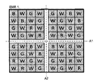
CFA600の個々のフィルタは、MRU602のような最小反復単位(MRU)にグループ分けされ、MRUは、矢印によって示すように垂直及び水平にタイル張りされてGFA600を形成する。最小反復単位は、その他の反復単位により少ない個々のフィルタがないような反復単位である。定められた色フィルタアレイは、いくつかの異なる反復単位を含むことができるが、反復単位は、より少ない個々のフィルタを含むアレイに別の反復単位がある場合に最小反復単位ではない。
The individual filters of CFA 600 are grouped into minimal repeating units (MRUs) such as
図6Bは、MRU602の実施形態を示している。MRU602は、横列及び縦列にグループ分けされた個々のフィルタのアレイである。MRU602は、iが1からM及びjが1からNに及ぶように、縦列を指標iで測定し、横列を指標jで測定したM縦列及びN横列を含む。例示的な実施形態において、MRU602は正方形であり、N=Mを意味するが、その他の実施形態において、Nは、Mに等しい必要はない。
FIG. 6B shows an embodiment of
MRU602は、I−IVに番号付されて右上から始まって反時計回りに配置された第1から第4の四分円を有する4つの四分円に分けることができ、四分円Iは上部右に、四分円IIは上部左に、四分円IIIは下部左に、四分円IVは下部右にある。以下に説明するように、MRU602のようなMRUを形成する1つの方法は、異なる四分円のMRU602よりも小さい複数の成分パターンを配置することである。MRU602はまた、直交して実質的にMRUを二等分する1組の軸線1及び2を含み、軸線1は、MRU602を上部と下部の半分に分けるが、軸線2は、MRUを左と右の半分に分ける。他の実施形態において、軸線の他の組が可能であり、軸線は、互いに直交している必要はなく、例えば、その他の実施形態において、MRUの対角線は、MRUの軸線を形成することができる。
The
図6Cは、MRUの一部の態様、特にこれらの対称、非対称、又は逆対称を説明するために本発明の開示に使用する専門用語を示している。図は、軸線の左側及び右側に赤色(R)及び青色(B)フィルタ位置を示している。左側のフィルタは下付き文字1(R1、B1等)を有するが、右側のフィルタは下付き文字2(R2、B2等)を有する。 FIG. 6C illustrates some terminology used in disclosing the present invention to describe some aspects of the MRU, particularly these symmetry, asymmetry, or antisymmetry. The figure shows red (R) and blue (B) filter positions on the left and right sides of the axis. The left filter has subscript 1 (R1, B1, etc.) while the right filter has subscript 2 (R2, B2, etc.).
横列604は、左側及び右側が軸線の回りで互いに鏡像であるように軸線の回りで物理的に及び連続的に対称である。横列604は、軸線に対する各色の位置が同じであるので物理的に対称であり、R1及びR2は軸線から同じ距離(xR1=xR2)であり、B1及びB2は軸線から同じ距離(xB1=xB2)である等々である。かつ横列はまた、色シーケンスが軸線に関して対称であるので連続的に対称であり、軸線から右に移動すると色シーケンスはRBGであり、軸線から左に移動すると色シーケンスは同じくRBGである。 Row 604 is physically and continuously symmetrical about the axis so that the left and right sides are mirror images of each other about the axis. Row 604 is physically symmetrical because the position of each color relative to the axis is the same, R1 and R2 are the same distance from the axis (xR1 = xR2), and B1 and B2 are the same distance from the axis (xB1 = xB2). And so on. And the rows are also continuously symmetric because the color sequence is symmetric about the axis, the color sequence is RBG when moving to the right from the axis, and the color sequence is also RBG when moving to the left from the axis.
横列606は、軸線の回りで物理的に対称ではないが、実質的に対称である一定の実施形態を示している。横列606は、軸線に対する各色の位置が同じではないので物理的に対称ではなく(すなわち、横列606は物理的に非対称である)、R1及びR2は、軸線から異なる距離(xR1≠xR2)であり、青色ピクセルB1及びB2は、軸線から異なる距離(xB1≠xB2)である等々である。しかし、例示的な実施形態は、物理的に対称ではないが、色シーケンスが軸線に関して対称であるので、例示的な実施形態は、それにもかかわらず連続的に対称であり、軸線から右に移動すると色シーケンスはRBGであり、同様に軸線から左に移動すると色シーケンスは同じくRBGである。
Row 606 illustrates certain embodiments that are not physically symmetric about the axis, but are substantially symmetric. Row 606 is not physically symmetric because the position of each color relative to the axis is not the same (ie,
横列608は、物理的に及び連続的に非対称である一定の実施形態を示し、すなわち、軸線の回りで連続的に対称でもなければ物理的に対称でもない。横列608は、軸線に対する各色の位置が同じではないので物理的に対称ではなく、R1及びR2は、軸線から異なる距離(xR1≠xR2)であり、青色ピクセルB1及びB2は、異なる距離(xB1≠xB2)である等々である。同様に横列は、色シーケンスが軸線に関して対称ではないので連続的に非対称であり、軸線から左に移動すると色シーケンスはRBGであるが、軸線から右に移動すると色シーケンスはBRGである。 Row 608 represents an embodiment that is physically and continuously asymmetric, i.e., neither continuously symmetrical nor physically symmetrical about the axis. Row 608 is not physically symmetrical because the position of each color relative to the axis is not the same, R1 and R2 are at different distances (xR1 ≠ xR2) from the axis, and blue pixels B1 and B2 are at different distances (xB1 ≠ xB2) and so on. Similarly, the rows are continuously asymmetric because the color sequence is not symmetric about the axis, and the color sequence is RBG when moving left from the axis, but the color sequence is BRG when moving right from the axis.
横列610は、物理的に非対称であり、かつ連続的に逆対称である一定の実施形態を示している。横列608は、軸線に対する各色の位置が同じでないので物理的に対称ではなく、R1及びR2は、軸線から異なる距離(xR1≠xR2)であり、青色ピクセルB1及びB2は、異なる距離(xB1≠xB2)等々である。同様に横列は、軸線の一方側の色シーケンスが軸線の他方側の色シーケンスの正反対であるので連続的に逆対称であり、軸線から左に移動すると色シーケンスはRBGであるが、軸線から右に移動すると色シーケンスはGBRである。 Row 610 illustrates an embodiment that is physically asymmetric and is continuously inversely symmetric. Row 608 is not physically symmetric because the position of each color relative to the axis is not the same, R1 and R2 are at different distances from the axis (xR1 ≠ xR2), and blue pixels B1 and B2 are at different distances (xB1 ≠ xB2). And so on. Similarly, the row is continuously inversely symmetric because the color sequence on one side of the axis is the exact opposite of the color sequence on the other side of the axis, and when moving from the axis to the left, the color sequence is RBG, but from the axis to the right When moving to, the color sequence is GBR.
図6Dは、8x8MRUにまとめることができる開示した4x4成分パターンを説明するために以下に使用する専門用語を示すが、専門用語はまた、異なる寸法の成分パターンを説明するのにも使用することができ、MRU自体又は全体として色フィルタアレイ(CFA)を説明するのにも使用することができる。メジャー対角線は上部左から下部右に延びるが、マイナー対角線は上部右から下部左に延びる。上部左から下部右に延びる4つのピクセルの長い対角線は、メジャー長い対角線として公知である。メジャー長い対角線の上では、上部左から下部右に延びる2つのピクセル対角線は、上側メジャー短い対角線として公知である。メジャー長い対角線よりも小さいと、上部左から下部右に延びる2つのピクセル対角線は、下側メジャー短い対角線として公知である。マイナー対角線に使用する専門用語は、図に示すものと同様であろう。本発明の開示は、メジャー対角線のみを説明するが、これは例示の目的に過ぎない。マイナー対角線を伴う実施形態は、代替実施形態であるので、これらは以下に説明しないが、これらは本発明の開示の一部として考えるべきである。 6D shows the terminology used below to describe the disclosed 4x4 component patterns that can be combined into an 8x8 MRU, but the terminology can also be used to describe component patterns of different dimensions. It can also be used to describe the MRU itself or the color filter array (CFA) as a whole. The major diagonal extends from the upper left to the lower right, while the minor diagonal extends from the upper right to the lower left. The long diagonal of four pixels extending from the upper left to the lower right is known as the major long diagonal. Above the major long diagonal, the two pixel diagonals extending from the upper left to the lower right are known as the upper major short diagonal. Two pixel diagonals extending from the upper left to the lower right below the major long diagonal are known as the lower major short diagonal. The terminology used for the minor diagonal will be similar to that shown in the figure. Although the present disclosure describes only the major diagonal, this is for illustrative purposes only. The embodiments with minor diagonals are alternative embodiments, so they are not described below, but should be considered as part of the disclosure of the present invention.
図6E〜図6Fは、チェッカー盤フィルタパターンの実施形態を示している。チェッカー盤パターンは、MRUを形成するアレイ又は成分パターンを形成するアレイの交互フィルタが同じ光応答、例えば、第1光応答を有するフィルタを有する1つである。チェッカー盤を形成するのに使用する第1光応答はまた、チェッカー盤光応答と呼ぶことができる。チェッカー盤光応答は、次に、MRUの個々のフィルタの実質的に半分を占める。例示的な実施形態において、チェッカー盤光応答は、白色又は全整色であるが、その他の実施形態において、チェッカー盤光応答は、緑色等の異なる可能性がある。以下に説明するように、チェッカー盤の一部でないものであるパターンの残りのスポットは、第1又はチェッカー盤光応答とは異なるものである第2、第3、及び第4光応答のフィルタで満たすことができる。 6E-6F illustrate an embodiment of a checkerboard filter pattern. The checkerboard pattern is one in which the array forming the MRU or the alternating filter of the array forming the component pattern has a filter with the same optical response, eg, a first optical response. The first optical response used to form the checkerboard can also be referred to as the checkerboard optical response. The checkerboard light response then accounts for substantially half of the individual filters of the MRU. In an exemplary embodiment, the checkerboard light response is white or fully chromatic, but in other embodiments, the checkerboard light response can be different, such as green. As will be described below, the remaining spots of the pattern that are not part of the checkerboard are the second, third, and fourth photoresponse filters that are different from the first or checkerboard photoresponse. Can be satisfied.
図6Eは、奇数の横列(j奇数)の偶数の縦列(i偶数)上にチェッカー盤光応答を有するフィルタを配置し、偶数の横列(j偶数)の奇数の縦列(i奇数)上にチェッカー盤光応答を有するフィルタを配置することによって形成されたチェッカー盤実施形態を示している。図6Fは、奇数の横列(j奇数)の奇数の縦列(i奇数)上にチェッカー盤光応答を有するフィルタを配置し、偶数の横列(j偶数)の偶数の縦列(i偶数)上にチェッカー盤光応答を有するフィルタを配置することによって形成されたチェッカー盤実施形態を示している。 FIG. 6E places a filter having a checkerboard photoresponse on an even number of rows (j even) of odd rows (j odd) and a checker on the odd columns (i odd) of even rows (j even). Fig. 5 illustrates a checkerboard embodiment formed by placing a filter having a panel light response. FIG. 6F places a filter with checkerboard light response on an odd number of rows (j odd), an odd number of columns (i odd), and a checker on an even number of rows (j even). Fig. 5 illustrates a checkerboard embodiment formed by placing a filter having a panel light response.
基本RGBW成分パターン
図7A〜図7Kは、図6Bに示す四分円の中に配置された4つの成分パターンの組を使用することによってMRUを形成するようにまとめることができる成分パターンの実施形態を示している。図7A〜図7Cは、成分パターンIと呼ばれる第1の成分パターン及びその変形のいくつかを示し、図7D〜図7Kは、成分パターンIIと呼ばれる第2の成分パターン及びその変形のいくつかを示している。図7A〜図7Kに示す成分パターンは、4つの組にまとめて8x8MRUを形成することができる4x4パターンであるが、その他の実施形態において、成分パターンは、4x4とは異なるサイズのものとすることができる。これらの他の成分パターンの実施形態の4つの組から形成されたMRUは、8x8とは異なるサイズを有することができる。
Basic RGBW Component Patterns FIGS. 7A-7K are embodiments of component patterns that can be combined to form an MRU by using a set of four component patterns arranged in the quadrant shown in FIG. 6B. Is shown. 7A-7C show a first component pattern called component pattern I and some of its variations, and FIGS. 7D-7K show a second component pattern called component pattern II and some of its variations. Show. The component patterns shown in FIGS. 7A to 7K are 4 × 4 patterns that can form 8 × 8 MRUs in groups of four, but in other embodiments, the component patterns have a size different from 4 × 4. Can do. An MRU formed from four sets of embodiments of these other component patterns can have a size different from 8x8.
一般的には、図7A〜図7Kに示す成分パターンは、チェッカー盤に使用する第1光応答、並びに非チェッカー盤フィルタに使用する第2、第3、及び第4光応答を含む1組の4つの光応答を使用する。例示的な実施形態において、第1又はチェッカー盤光応答は、全整色又は白色(W)であり、第2、第3、及び第4光応答は、赤色(R)、緑色(G)、及び青色(B)の中から選択される。他の実施形態は、勿論、光応答の異なる組を使用することができる。例えば、その他の実施形態は、シアン(C)、マゼンタ(M)、及びイエロー(Y)フィルタ、透明(すなわち、無色)フィルタ、赤外線フィルタ、紫外線フィルタ、X線フィルタなどを含むことができる。 In general, the component patterns shown in FIGS. 7A-7K include a set of first photoresponses used for a checkerboard and second, third, and fourth photoresponses used for non-checkerboard filters. Four light responses are used. In an exemplary embodiment, the first or checkerboard light response is fully toned or white (W), and the second, third, and fourth light responses are red (R), green (G), And blue (B). Other embodiments can, of course, use different sets of light responses. For example, other embodiments can include cyan (C), magenta (M), and yellow (Y) filters, transparent (ie, colorless) filters, infrared filters, ultraviolet filters, x-ray filters, and the like.
例示的な実施形態において、非チェッカー盤フィルタ、すなわち、第2、第3、及び第4光応答のフィルタの数は、できるだけほぼ等しくなるようにされる。正確な均等性は、非チェッカー盤フィルタの数を割り当てるべき光応答の数で均等に割り切れる実施形態で達成することができるが、単に近似的な均等性は、非チェッカー盤フィルタの数を割り当てるべき光応答の数で均等に割り切れない実施形態で達成することができる。他の実施形態において、第2、第3、及び第4光応答の各々のフィルタは、非チェッカー盤フィルタの0%〜100%、並びにあらゆる個々の数又はこれらの間の部分的範囲で変化させることができる。 In the exemplary embodiment, the number of non-checkerboard filters, ie, the second, third, and fourth photoresponse filters, is made to be as nearly equal as possible. Exact equality can be achieved in embodiments that are evenly divisible by the number of light responses to which the number of non-checkerboard filters should be assigned, but only approximate equality should be assigned the number of non-checkerboard filters. This can be achieved in embodiments that are not evenly divisible by the number of light responses. In other embodiments, each filter of the second, third, and fourth photoresponses varies from 0% to 100% of the non-checkerboard filter, and any individual number or subrange between them. be able to.
図7A〜図7Cは、成分パターンI及びその変形のいくつかを示している。図7Aは、成分パターンIを示し、成分パターンIは、そのフィルタアレイのために対角線方向の色エイリアシングを受ける可能性がある。成分パターンIを単独に使用してより大きいMRUを構成する場合に、同じ対角色エイリアシング問題が存続することになる。これらの成分パターンのいくつかの変形は、色エイリアシングを低減するのを補助することができる。 7A-7C show component pattern I and some of its variations. FIG. 7A shows a component pattern I, which can undergo diagonal color aliasing due to its filter array. If component pattern I is used alone to construct a larger MRU, the same diagonal color aliasing problem will persist. Some variations of these component patterns can help reduce color aliasing.
図7Bは、成分パターンIの変形である成分パターンI−1を示している。成分パターンIとは対照的に、2つの主要な修正があり、緑色(G)ピクセルは、ここではメジャー長い対角線に移動し、青色(B)ピクセルカプレットBB及び赤色(R)ピクセルカプレットRRは、メジャー短い対角線に移動する。より具体的には、BBカプレットは、ここでは上側メジャー短い対角線を占め、RRカプレットは、ここでは下側メジャー短い対角線を占める。これらの修正の代替手段は、メジャー長い対角線の一部分のみを占めるGピクセルを有するBB及びRRカプレットのような対角線の反転を含むことができる。 FIG. 7B shows a component pattern I-1 that is a modification of the component pattern I. In contrast to component pattern I, there are two major modifications: the green (G) pixel now moves to the major long diagonal, the blue (B) pixel couplet BB and the red (R) pixel couplet RR are Move to the major short diagonal. More specifically, the BB couplet now occupies the upper major short diagonal, and the RR couplet here occupies the lower major short diagonal. Alternatives to these modifications can include diagonal inversions such as BB and RR couplets with G pixels occupying only a portion of the major long diagonal.
図7Cは、成分パターンIの別の変形である成分パターンI−2を示している。このパターンは、カプレットBBがここでは下側メジャー短い対角線を占め、カプレットRRがここでは上側メジャー短い対角線を占めることを除いて成分パターンI−1に類似している。代替手段は、上述したように類似している。 FIG. 7C shows a component pattern I-2, which is another variation of the component pattern I. This pattern is similar to the component pattern I-1 except that the couplet BB now occupies the lower major short diagonal and the couplet RR now occupies the upper major short diagonal. The alternative means are similar as described above.
図7D〜図7Kは、成分パターンII及びその変形のいくつかを示している。図7Dは成分パターンIIを示し、成分パターンIIは、成分パターンIのように、対角線方向の色エイリアシングを受ける可能性がある。成分パターンIIを単独に使用してより大きいMRUを構成する場合に、同じ対角線色エイリアシング問題が存続することになる。これらの成分パターンのいくつかの変形は、色エイリアシングを低減するのを補助することができる。 7D-7K illustrate component pattern II and some of its variations. FIG. 7D shows the component pattern II, which, like the component pattern I, may undergo diagonal color aliasing. The same diagonal color aliasing problem will persist if component pattern II is used alone to construct a larger MRU. Some variations of these component patterns can help reduce color aliasing.
図7Eは、成分パターンIIの変形である成分パターンII―1を示している。成分パターンIIとは対照的に、2つの主要な修正があり、Gピクセルは移動してメジャー長い対角線全体を占め、BR(又はこれに代えてRB)カプレットはメジャー短い対角線に移動する。これらの修正の代替手段は、第1の実施形態に関連した開示に説明したものに類似している。 FIG. 7E shows a component pattern II-1 that is a modification of the component pattern II. In contrast to component pattern II, there are two major modifications: the G pixel moves to occupy the entire major long diagonal, and the BR (or alternatively RB) couplet moves to the major short diagonal. Alternatives to these modifications are similar to those described in the disclosure relating to the first embodiment.
図7Fは、成分パターンIIの別の変形である成分パターンII−2を示している。このパターンは、カプレットRBをカプレットBRの代わりに使用することを除いて成分パターンII−1に類似している。代替手段は、上述したように類似している。 FIG. 7F shows a component pattern II-2, which is another variation of the component pattern II. This pattern is similar to component pattern II-1 except that couplet RB is used instead of couplet BR. The alternative means are similar as described above.
半無作為化によるRGBW成分パターン
色エイリアシングの低減を改善するために、上に開示した基本RGBW成分パターンは、より複雑な規則によって更に修正することができる。上に開示したRGBW成分パターンにおけるように、第1光応答(図示の実施形態ではW)は、依然としてチェッカー盤パターンを形成するが、第2、第3、及び第4光応答(これらの実施形態ではR、G、及びB)を有するフィルタは、得られるMRUパターンが、より無作為に現れるが依然として一定の規則に従うように、より無作為に割り当てられる。従って、以下に示す実施形態に対して開示する修正処理は、半無作為化と呼ばれる。例示していない他の実施形態において、第2、第3、及び第4光応答は、完全に無作為に割り当てることができる。非チェッカー盤光応答フィルタ、すなわち、第2、第3、及び第4光応答を有するフィルタのアレイにおける無作為化の増大は、色エイリアシングを低減するためには望ましい。
In order to improve the reduction of RGBW component pattern color aliasing due to semi-randomization, the basic RGBW component pattern disclosed above can be further modified by more complex rules. As in the RGBW component pattern disclosed above, the first light response (W in the illustrated embodiment) still forms a checkerboard pattern, but the second, third, and fourth light responses (these embodiments). Now filters with R, G, and B) are assigned more randomly so that the resulting MRU pattern appears more randomly but still follows certain rules. Accordingly, the correction process disclosed for the embodiment shown below is called semi-randomization. In other embodiments not illustrated, the second, third, and fourth photoresponses can be assigned completely randomly. Increasing randomization in a non-checkerboard photoresponsive filter, i.e., an array of filters with second, third, and fourth photoresponses, is desirable to reduce color aliasing.
図7Gは、成分パターンIIの変形である成分パターンII−3を示している。この成分パターンのメジャー長い対角線は、成分パターンII及び成分パターンII−1又はII−2の混合である。メジャー長い対角線に沿って、交互BRの代わりに又は全てGであると、左上はBであり、右下はRであるが、2つの中間ピクセルはGである。上側及び下側メジャー短い対角線は、成分パターンII−2と同じである。代替手段は、上述したように類似している。 FIG. 7G shows a component pattern II-3 that is a modification of the component pattern II. The major long diagonal of this component pattern is a mixture of component pattern II and component pattern II-1 or II-2. Along the major long diagonal, instead of alternating BR or all G, the upper left is B and the lower right is R, but the two middle pixels are G. The upper and lower major short diagonals are the same as component pattern II-2. The alternative means are similar as described above.
図7Hは、成分パターンIIの別の変形である成分パターンII−4を示している。このパターンは、カプレットRBがここではメジャー長い対角線の2つの中間ピクセルを占めることを除いて成分パターンII−2に類似している。代替手段は、上述したように類似している。 FIG. 7H shows component pattern II-4, which is another variation of component pattern II. This pattern is similar to the component pattern II-2 except that the couplet RB now occupies two intermediate pixels of a major long diagonal. The alternative means are similar as described above.
図7Iは、成分パターンIIの別の変形である成分パターンII−5を示している。いくつかの修正をここで行う。第1に、メジャー長い対角線に沿った色の順番は、BRからRBに逆にする。第2に、上側メジャー短い対角線は、ここではカプレットGGの代わりにカプレットBGを含む。第3に、下側メジャー短い対角線は、ここではカプレットGGの代わりにカプレットGRを含む。代替手段は、上述したように類似している。 FIG. 7I shows component pattern II-5, which is another variation of component pattern II. Here are some fixes. First, the order of colors along the major long diagonal is reversed from BR to RB. Second, the upper major short diagonal now includes the couplet BG instead of the couplet GG. Third, the lower major short diagonal now includes the couplet GR instead of the couplet GG. The alternative means are similar as described above.
図7Jは、成分パターンIIの別の変形である成分パターンII−6を示している。成分パターンII−6は、上側メジャー短い対角線がここではカプレットGGの代わりにカプレットGRを含み、下側メジャー短い対角線がここではカプレットGGの代わりにカプレットBGを含むことを除いて成分パターンII−5に類似している。代替手段は、上述したように類似している。 FIG. 7J shows component pattern II-6, which is another variation of component pattern II. Component pattern II-6 is component pattern II-5 except that the upper major short diagonal now contains couplet GR instead of couplet GG and the lower major short diagonal now contains couplet BG instead of couplet GG. Is similar. The alternative means are similar as described above.
図7Kは、成分パターンIIの別の変形である成分パターンII−7を示している。このパターンは、色パターンがここではRBRBの代わりにRBBBであるようにメジャー長い対角線のRフィルタがBフィルタで置換されることを除いて成分パターンII−6に類似している。成分パターンII−3〜II−7は、半無作為化処理の例に過ぎない。図面に示していないより多くの例があるが、依然として本発明の開示の一部である。 FIG. 7K shows a component pattern II-7, which is another variation of the component pattern II. This pattern is similar to component pattern II-6 except that the major long diagonal R filter is replaced with a B filter so that the color pattern is now RBBB instead of RBRB. Component patterns II-3 to II-7 are merely examples of semi-randomization processing. There are more examples not shown in the drawings, but they are still part of the present disclosure.
第1のRGBW MRU実施形態及び代替手段
図8Aは、成分パターンI及びI−1を使用する赤色−緑色−青色−白色(RGBW)MRUの実施形態を示している。成分パターンI−1は、第1及び第3の四分円を占め、成分パターンIは、第2及び第4の四分円を占める。得られるMRUは、軸線A2の回りで連続的に対称であるが軸線A1の回りで連続的に非対称である非チェッカー盤光応答(第2、第3、及び第4光応答)を有する。
First RGBW MRU Embodiment and Alternatives FIG. 8A shows an embodiment of a red-green-blue-white (RGBW) MRU that uses component patterns I and I-1. The component pattern I-1 occupies the first and third quadrants, and the component pattern I occupies the second and fourth quadrants. The resulting MRU has non-checkerboard photoresponses (second, third, and fourth photoresponses) that are continuously symmetrical about axis A2 but are continuously asymmetric about axis A1.
本発明の一部の実施形態の代替手段がある。第1に、成分パターンタイプへの四分円割り当ては、変更することができる。例えば、成分Iは、第2及び第4の四分円、又は第1及び第2の四分円などを占めることができるのに対して、成分パターンI−1は、残りの四分円を占める。第2に、成分パターンの数も変更することができる。例えば、3つの成分パターンI及び1つの成分パターンI−1が存在することができ、又は逆も同様である。成分パターンI−1のような1つの成分パターンのみが存在することができる。四分円割り当て及び成分パターンの様々な組合せは、多くの代替実施形態を生成することができ、代替実施形態は、本明細書では詳細に全てを示すか又は列挙しているとは限らず、それにもかかわらず本発明の開示の一部である。 There are alternatives to some embodiments of the invention. First, the quadrant assignment to the component pattern type can be changed. For example, component I can occupy the second and fourth quadrants, or the first and second quadrants, etc., whereas component pattern I-1 can represent the remaining quadrants. Occupy. Second, the number of component patterns can also be changed. For example, there can be three component patterns I and one component pattern I-1, or vice versa. There can be only one component pattern, such as component pattern I-1. Various combinations of quadrant assignments and component patterns can produce many alternative embodiments, which are not all shown or listed in detail herein, Nevertheless, it is part of the disclosure of the present invention.
第2のRGBW MRU実施形態及び代替手段
図8Bは、成分パターンII及びII−1を使用するRGBW MRUの第2の実施形態を示している。成分パターンII−1は、第1及び第3の四分円を占め、成分パターンIIは、第2及び第4の四分円を占める。得られるMRUは、軸線A1及び軸線A2の両方の回りで連続的に対称である非チェッカー盤光応答を有する(第2、第3、及び第4光応答)。MRUのこの第2の実施形態の代替手段は、第1の実施形態に関連付けられた開示において上述したものに類似している。
Second RGBW MRU Embodiment and Alternatives FIG. 8B shows a second embodiment of an RGBW MRU that uses component patterns II and II-1. The component pattern II-1 occupies the first and third quadrants, and the component pattern II occupies the second and fourth quadrants. The resulting MRU has a non-checkerboard optical response that is continuously symmetrical about both axis A1 and axis A2 (second, third, and fourth optical responses). Alternatives to this second embodiment of the MRU are similar to those described above in the disclosure associated with the first embodiment.
第3のRGBW MRU実施形態及び代替手段
図8Cは、成分パターンII及びII−2を使用するRGBW MRUの第3の実施形態を示している。2つの成分パターンII及び2つの成分パターンII−2を使用して最終MRUを構成する。成分パターンII−2は、第1及び第3の四分円を占め、成分パターンIIは、第2及び第4の四分円を占める。得られるMRUは、軸線A1及び軸線A2の両方の回りで連続的に非対称である非チェッカー盤光応答(第2、第3、及び第4光応答)を有する。この第3のMRU実施形態の代替手段は、上述したものに類似している。
Third RGBW MRU Embodiment and Alternatives FIG. 8C shows a third embodiment of an RGBW MRU that uses component patterns II and II-2. Two component patterns II and two component patterns II-2 are used to construct the final MRU. The component pattern II-2 occupies the first and third quadrants, and the component pattern II occupies the second and fourth quadrants. The resulting MRU has non-checkerboard photoresponses (second, third, and fourth photoresponses) that are continuously asymmetric about both axis A1 and axis A2. Alternatives to this third MRU embodiment are similar to those described above.
第4のRGBW MRU実施形態及び代替手段
図8Dは、成分パターンI及びI−2を使用するRGBW MRUの第4の実施形態を示している。2つの成分パターンI及び2つの成分パターンI−2を使用して、成分パターンI−2は、第1及び第3の四分円を占め、成分パターンIは、第2及び第4の四分円を占める。得られるMRUは、軸線A1及び軸線A2の両方の回りで連続的に非対称である非チェッカー盤光応答(第2、第3、及び第4光応答)を有する。この第4のMRU実施形態の代替手段は、上述したものに類似している。
Fourth RGBW MRU Embodiment and Alternatives FIG. 8D shows a fourth embodiment of an RGBW MRU that uses component patterns I and I-2. Using the two component patterns I and the two component patterns I-2, the component pattern I-2 occupies the first and third quadrants, and the component pattern I includes the second and fourth quadrants. Occupy the yen. The resulting MRU has non-checkerboard photoresponses (second, third, and fourth photoresponses) that are continuously asymmetric about both axis A1 and axis A2. Alternatives to this fourth MRU embodiment are similar to those described above.
第5のRGBW MRU実施形態及び代替手段
図8Eは、半無作為化から生じる成分パターン、具体的には成分パターンII−3及びII−7を使用するRGBW MRUの第5の実施形態を示している。成分パターンII−7は、第1及び第3の四分円を占め、成分パターンII−3は、第2及び第4の四分円を占める。得られるMRUは、軸線A1及び軸線A2の両方の回りで連続的に非対称である非チェッカー盤光応答(第2、第3、及び第4光応答)を有する。この第5のMRU実施形態の代替手段は、上述したものに類似している。
Fifth RGBW MRU Embodiment and Alternatives FIG. 8E shows a fifth embodiment of an RGBW MRU using component patterns resulting from semi-randomization, specifically component patterns II-3 and II-7. Yes. The component pattern II-7 occupies the first and third quadrants, and the component pattern II-3 occupies the second and fourth quadrants. The resulting MRU has non-checkerboard photoresponses (second, third, and fourth photoresponses) that are continuously asymmetric about both axis A1 and axis A2. Alternatives to this fifth MRU embodiment are similar to those described above.
第6のRGBW MRU実施形態及び代替手段
図8Fは、半無作為化から生じる成分パターン、具体的には成分パターンII−3、II−4、II−5、及びII−6を使用するRGBW MRUの第5の実施形態を示している。成分パターンII−5は、第1の四分円を占め、成分パターンII−3は、第2の四分円を占め、成分パターンII−6は、第3の四分円を占め、成分パターンII−4は、第4の四分円を占める。得られるMRUは、軸線A1及び軸線A2の両方の回りで連続的に対称である非チェッカー盤光応答(第2、第3、及び第4光応答)を有する。この第5のMRU実施形態の代替手段は、上述したものに類似している。
Sixth RGBW MRU Embodiment and Alternative FIG. 8F shows RGBW MRUs using component patterns resulting from semi-randomization, specifically component patterns II-3, II-4, II-5, and II-6. The 5th Embodiment of this is shown. Component pattern II-5 occupies the first quadrant, component pattern II-3 occupies the second quadrant, component pattern II-6 occupies the third quadrant, and component pattern II-4 occupies the fourth quadrant. The resulting MRU has non-checkerboard photoresponses (second, third, and fourth photoresponses) that are continuously symmetrical about both axis A1 and axis A2. Alternatives to this fifth MRU embodiment are similar to those described above.
RGB−IR成分パターン
CCD又はCMOS画像センサの赤外線(IR)応答を改善しながら色エイリアシングの低減を改善するために、図7G〜図7Kにおいて開示したRGBW成分パターンは、IRフィルタを含むように更に修正することができる。得られるRGB−IRパターンは、無作為であると思われるが、依然として一定の規則に従う。赤色(R)フィルタは、赤色及び赤外線光の両方がそのそれぞれの感光性領域(例えば、光ダイオード)を通過することを可能にし、緑色(G)フィルタは、緑色及び赤外線光の両方が通過することを可能にし、青色(B)フィルタは、青色及び赤外線光の両方が通過することを可能にすることに注意されたい。一部の実施形態において、赤外線(IR)ピクセルは、単に赤外線光が通過することを可能にするRGBフィルタ材料の組合せで覆われる。
RGB-IR Component Pattern To improve the reduction of color aliasing while improving the infrared (IR) response of a CCD or CMOS image sensor, the RGBW component pattern disclosed in FIGS. 7G-7K further includes an IR filter. Can be corrected. The resulting RGB-IR pattern appears to be random but still follows certain rules. A red (R) filter allows both red and infrared light to pass through its respective photosensitive area (eg, a photodiode), and a green (G) filter passes both green and infrared light. Note that the blue (B) filter allows both blue and infrared light to pass through. In some embodiments, the infrared (IR) pixels are covered with a combination of RGB filter materials that simply allow infrared light to pass through.
説明するRGB−IR成分パターンにおいて、第1の(チェッカー盤)光応答は、白色の代わりに緑色であり、第2、第3、及び第4光応答は、赤色、青色、及び赤外線の中から選択される。他の実施形態は、勿論、異なる組の光応答を使用することができる。例えば、その他の実施形態は、シアン(C)、マゼンタ(M)、及びイエロー(Y)フィルタ、透明(すなわち、無色)フィルタ、赤外線フィルタ、紫外線フィルタ、X線フィルタなどを含むことができる。 In the described RGB-IR component pattern, the first (checkerboard) light response is green instead of white, and the second, third, and fourth light responses are among red, blue, and infrared. Selected. Other embodiments can of course use different sets of light responses. For example, other embodiments can include cyan (C), magenta (M), and yellow (Y) filters, transparent (ie, colorless) filters, infrared filters, ultraviolet filters, x-ray filters, and the like.
図9A〜図9Fは、図6Bに示す四分円の中に配置された4つの組を使用することによってRGB−IR MRUを形成するようにまとめることができる赤色−緑色−青色−赤外線(RGB−IR)の実施形態を示している。図9Aは、成分パターンIの変形である成分パターンI−3を示している。成分パターンIとは対照的に、成分I−3は、2つの主要な修正を有し、成分パターンIの緑色(G)ピクセルは、赤外線(IR)ピクセルで置換されており、白色(W)(透明又は全整色とも呼ばれる)ピクセルは、緑色(G)ピクセルで置換される。IR−IRカプレットは、上側メジャー短い対角線及び下側メジャー短い対角線の両方を占めるが、メジャー長い対角線は、上側左コーナにBBカプレット及び下側右コーナにRRカプレットを含む。 9A-9F are red-green-blue-infrared (RGB) that can be grouped together to form an RGB-IR MRU by using four sets arranged in the quadrant shown in FIG. 6B. -IR) embodiment. FIG. 9A shows a component pattern I-3 that is a modification of the component pattern I. In contrast to component pattern I, component I-3 has two major modifications, the green (G) pixel of component pattern I has been replaced with an infrared (IR) pixel, and white (W) Pixels (also called transparent or full color matching) are replaced with green (G) pixels. The IR-IR couplet occupies both the upper major short diagonal and the lower major short diagonal, but the major long diagonal includes the BB couplet in the upper left corner and the RR couplet in the lower right corner.
図9Aの成分パターンI−3は、8X8又はそれよりも大きいMRUを構成するのに使用することができる以上に、成分パターンの唯一の例である。上述の成分パターンのいずれも、同様に修正することができる。すなわち、RGBW成分パターンI、I−1、I−2、II、II−1、II−2、II−3、II−4、II−5、II−6、II−7、及びこられの代替手段のいずれも、最初に緑色(G)ピクセルを赤外線(IR)ピクセルで置換、次に、白色(W)ピクセルを緑色(G)ピクセルで置換することによって修正することができる。言い換えると、RGBW成分パターンI、I−1、I−2、II、II−1、II−2、II−3、II−4、II−5、II−6、II−7、及びこられの代替手段は、第1の(チェッカー盤)光応答が、白色の代わりに緑色であり、かつ第2、第3、及び第4光応答が、赤色、青色、及び赤外線の中から選択されるように修正することができる。以下は、このような修正を実施するいくつかの例示的な成分パターン及び得られるMRUである。 The component pattern I-3 in FIG. 9A is the only example of a component pattern beyond that it can be used to construct an 8 × 8 or larger MRU. Any of the above-described component patterns can be similarly modified. That is, RGBW component patterns I, I-1, I-2, II, II-1, II-2, II-3, II-4, II-5, II-6, II-7, and alternatives thereof Any of the means can be modified by first replacing the green (G) pixel with an infrared (IR) pixel and then replacing the white (W) pixel with a green (G) pixel. In other words, RGBW component patterns I, I-1, I-2, II, II-1, II-2, II-3, II-4, II-5, II-6, II-7, and these An alternative is that the first (checkerboard) light response is green instead of white and the second, third and fourth light responses are selected from among red, blue and infrared. Can be corrected. The following are some example component patterns and resulting MRUs that implement such modifications.
図9Bは、成分パターンIの別の変形である成分パターンI−4を示している。このパターンは、カプレットRRがここではメジャー長い対角線の上側左コーナを占め、カプレットBBがここでは下側右コーナを占めることを除いて成分パターンI−3に類似している。 FIG. 9B shows a component pattern I-4, which is another variation of the component pattern I. This pattern is similar to component pattern I-3 except that the couplet RR now occupies the upper left corner of the major long diagonal and the couplet BB now occupies the lower right corner.
図9Cは、成分パターンIの別の変形である成分パターンI−5を示している。成分パターンI−5は、IRピクセルがメジャー長い対角線に移動し、RRカプレットがここでは上側メジャー短い対角線を占め、BBカプレットがここでは下側メジャー短い対角線を占めることを除いて成分パターンI−3に類似している。 FIG. 9C shows a component pattern I-5, which is another variation of the component pattern I. Component pattern I-5 is component pattern I-3 except that the IR pixel moves to the major long diagonal, the RR couplet now occupies the upper major short diagonal, and the BB couplet now occupies the lower major short diagonal. Is similar.
図9Dは、カプレットBBが上側メジャー短い対角線を占め、カプレットRRが下側メジャー短い対角線を占めることを除いて成分パターンI−5に類似している成分パターンI−6を示している。 FIG. 9D shows a component pattern I-6 that is similar to the component pattern I-5 except that the couplet BB occupies the upper major short diagonal and the couplet RR occupies the lower major short diagonal.
図9Eは、成分パターンIIの別の修正である成分パターンI−8を示している。成分パターンIIとは対照的に、2つの主要な修正があり、成分パターンIIの緑色(G)ピクセルは、赤外線(IR)ピクセルで置換されており、白色(W)ピクセルは、緑色(G)ピクセルで置換される。より具体的には、IR−IRカプレットは、上側メジャー短い対角線及び下側メジャー短い対角線の両方を占めるが、メジャー長い対角線は、上側左コーナにBRカプレット及び下側右コーナにBRカプレットを含む。 FIG. 9E shows component pattern I-8, which is another modification of component pattern II. In contrast to component pattern II, there are two major modifications: the green (G) pixel of component pattern II has been replaced with an infrared (IR) pixel and the white (W) pixel is green (G) Replaced by pixel. More specifically, the IR-IR couplet occupies both the upper major short diagonal and the lower major short diagonal, but the major long diagonal includes the BR couplet at the upper left corner and the BR couplet at the lower right corner.
図9Fは、成分パターンIIの別の変形である成分パターンII−9を示している。このパターンは、IRピクセルがメジャー長い対角線に移動し、BRカプレットがここでは上側メジャー短い対角線を占め、別のBRカプレットがここでは下側メジャー短い対角線を占めることを除いて成分パターンII−8に類似している。 FIG. 9F shows a component pattern II-9, which is another variation of the component pattern II. This pattern follows the component pattern II-8 except that the IR pixel moves to the major long diagonal, the BR couplet now occupies the upper major short diagonal, and another BR couplet now occupies the lower major short diagonal. It is similar.
第1のRGB−IR MRU実施形態及び代替手段
図10Aは、半無作為化から生じる成分パターンを含めることを意味する成分パターンI−3〜I−6を使用する赤色−緑色−青色−赤外線(RGB−IR)MRUの第1の実施形態を示している。成分パターンI−5は第1の四分円、成分パターンI−3は第2の四分円、成分パターンI−6は第3の四分円、成分パターンI−4は第4の四分円を占める。得られるMRUは、軸線A1及び軸線A2の両方の回りで連続的に非対称である非チェッカー盤光応答(第2、第3、及び第4光応答)を有する。四分円割り当て及び成分パターン数の様々な組合せは、多くの代替実施形態を生成することができ、これらは、本明細書に詳細に列挙することなく依然として本発明の開示の一部である。
First RGB-IR MRU Embodiment and Alternative FIG. 10A shows red-green-blue-infrared (IR) using component patterns I-3 to I-6, meant to include component patterns resulting from semi-randomization. 1 shows a first embodiment of an RGB-IR) MRU. Component pattern I-5 is the first quadrant, component pattern I-3 is the second quadrant, component pattern I-6 is the third quadrant, and component pattern I-4 is the fourth quadrant. Occupy the yen. The resulting MRU has non-checkerboard photoresponses (second, third, and fourth photoresponses) that are continuously asymmetric about both axis A1 and axis A2. Various combinations of quadrant assignments and number of component patterns can produce many alternative embodiments, which are still part of the present disclosure without being listed in detail herein.
明らかなように、図10Aに示す第1のRGB−IR MRU実施形態は、図8Dに示す第4のRGBW実施形態の修正バージョンである。すなわち、第1のRGB−IR実施形態は、第4のRGBW MRU実施形態を取り、緑色(G)ピクセルを赤外線(IR)ピクセルで置換し、白色(W)ピクセルを緑色(G)ピクセルで置換することによって形成することができる。 As is apparent, the first RGB-IR MRU embodiment shown in FIG. 10A is a modified version of the fourth RGBW embodiment shown in FIG. 8D. That is, the first RGB-IR embodiment takes the fourth RGBW MRU embodiment and replaces green (G) pixels with infrared (IR) pixels and replaces white (W) pixels with green (G) pixels. Can be formed.
第2のRGB−IR MRU実施形態及び代替手段
図10Bは、半無作為化から生じる成分パターンを含めることを意味する成分パターンII−8及びII−9を使用する第2のRGB−IR MRU実施形態を示している。成分パターンII−9は第1及び第3の四分円を占めるが、成分パターンII−8は第2及び第4の四分円を占める。得られるMRUは、軸線A1及び軸線A2の両方の回りで連続的に非対称である非チェッカー盤光応答(第2、第3、及び第4光応答)を有する。四分円割り当て及び成分パターン数の様々な組合せは、多くの代替実施形態を生成することができ、これらは、本明細書に詳細に列挙することなく依然として本発明の開示の一部と考えられる。
Second RGB-IR MRU Embodiment and Alternative FIG. 10B shows a second RGB-IR MRU implementation using component patterns II-8 and II-9 meant to include component patterns resulting from semi-randomization. The form is shown. Component pattern II-9 occupies the first and third quadrants, while component pattern II-8 occupies the second and fourth quadrants. The resulting MRU has non-checkerboard photoresponses (second, third, and fourth photoresponses) that are continuously asymmetric about both axis A1 and axis A2. Various combinations of quadrant assignments and number of component patterns can produce many alternative embodiments, which are still considered part of the disclosure of the present invention without being listed in detail herein. .
明らかなように、第2のRGB−IR MRU実施形態は、図8Bに示す第2のRGBW MRU実施形態の修正バージョンである。すなわち、第2のRGB−IR MRU実施形態は、第2のRGBW MRU実施形態を取り、緑色(G)ピクセルを赤外線(IR)ピクセルで置換し、白色(W)ピクセルを緑色(G)ピクセルで置換することによって形成することができる。上述のRGBW MRU実施形態のいずれも、IRピクセルを含むように同様に修正することができる。 As is apparent, the second RGB-IR MRU embodiment is a modified version of the second RGBW MRU embodiment shown in FIG. 8B. That is, the second RGB-IR MRU embodiment takes the second RGBW MRU embodiment and replaces green (G) pixels with infrared (IR) pixels and white (W) pixels with green (G) pixels. It can be formed by substitution. Any of the RGBW MRU embodiments described above can be similarly modified to include IR pixels.
第3のRGB−IR MRU実施形態及び代替手段
図10Cは、半無作為化から生じる成分パターンを含めることを意味する成分パターンII−8及びII−9を使用する赤外線MRUの第3のRGB−IR MRU実施形態を示している。成分パターンII−9は第1及び第3の四分円に位置決めされるが、成分パターンII−8は第2及び第4の四分円に位置決めされる。得られるMRUは、軸線A1及び軸線A2の両方の回りで連続的に対称である非チェッカー盤光応答(第2、第3、及び第4光応答)を有する。
Third RGB-IR MRU Embodiment and Alternative FIG. 10C shows a third RGB- infrared MRU using component patterns II-8 and II-9, which is meant to include component patterns resulting from semi-randomization. Fig. 2 illustrates an IR MRU embodiment. Component pattern II-9 is positioned in the first and third quadrants, while component pattern II-8 is positioned in the second and fourth quadrants. The resulting MRU has non-checkerboard photoresponses (second, third, and fourth photoresponses) that are continuously symmetrical about both axis A1 and axis A2.
一部の実施形態において、成分パターン及び得られるRGB−IR MRUは、緑色(G)、青色(B)、赤色(R)、及び赤外線(IR)ピクセルの比率を決める構成の第1の規則に従って構成することができる。一実施形態において、構成の第1の規則は、成分パターンが、約50%緑色フィルタ、12.5%青色フィルタ、12.5%赤色フィルタ、及び25%赤外線フィルタを含むように指示することができる。このフィルタ比率は、3次元(3D)撮像のようなある一定の用途において有益とすることができる。 In some embodiments, the component pattern and the resulting RGB-IR MRU are in accordance with a first rule of configuration that determines the ratio of green (G), blue (B), red (R), and infrared (IR) pixels. Can be configured. In one embodiment, the first rule of configuration directs the component pattern to include approximately 50% green filter, 12.5% blue filter, 12.5% red filter, and 25% infrared filter. it can. This filter ratio can be beneficial in certain applications, such as three-dimensional (3D) imaging.
上に示すように、成分パターンI−3〜I−6、II−8、及びII−9の各々と、得られる第1及び第2のRGB−IR MRUの各々とは、この規則に従う。すなわち、成分パターンI−3〜I−6、II−8、及びII−9の各々は、50%緑色フィルタ、12.5%青色フィルタ、12.5%赤色フィルタ、及び25%赤外線フィルタを有する。同様に、第1及び第2のRGB−IR MRUの両方も、50%緑色ピクセル、12.5%青色ピクセル、12.5%赤色ピクセル、及び25%赤外線ピクセルを含む。しかし、一部の実施形態において、成分パターン自体は、得られるRGB−IR MRUが従うという条件の下で、構成の第1の規則に従う必要はない。すなわち、成分パターンの更に別の無作為化は、得られる色及びIRフィルタアレイパターンが依然として構成の第1の規則に従う限り実施することができる。 As indicated above, each of the component patterns I-3 to I-6, II-8, and II-9 and each of the resulting first and second RGB-IR MRUs follows this rule. That is, each of the component patterns I-3 to I-6, II-8, and II-9 includes a 50% green filter, a 12.5% blue filter, a 12.5% red filter, and a 25% infrared filter. . Similarly, both the first and second RGB-IR MRUs include 50% green pixels, 12.5% blue pixels, 12.5% red pixels, and 25% infrared pixels. However, in some embodiments, the component pattern itself need not follow the first rule of construction, provided that the resulting RGB-IR MRU follows. That is, yet another randomization of the component pattern can be performed as long as the resulting color and IR filter array pattern still follows the first rule of construction.
第4のRGB−IR MRU実施形態及び代替手段
一部の実施形態において、成分パターン及び得られるRGB−IR MRUは、より低密度の赤外線(IR)ピクセルを含む構成の第2の規則に従って構成することができる。一実施形態において、構成の第2の規則は、パターンが、約50%緑色ピクセル、18.75%青色ピクセル、18.75%赤色ピクセル、及び12.5%赤外線ピクセルを含むように決めることができる。構成の第2の規則が与えるような比率は、暗視撮像のようなある一定の用途において有益とすることができる。
Fourth RGB-IR MRU embodiment and alternatives In some embodiments, the component pattern and the resulting RGB-IR MRU are configured according to a second rule of configuration that includes lower density infrared (IR) pixels. be able to. In one embodiment, the second rule of construction determines that the pattern includes approximately 50% green pixels, 18.75% blue pixels, 18.75% red pixels, and 12.5% infrared pixels. it can. The ratio as given by the second rule of construction can be beneficial in certain applications such as night vision imaging.
図11A〜図11Bは、低密度IR成分パターンの実施形態及びMRUの対応する実施形態を示している。図11Aは、低密度IR成分パターンを示している。図11Bは、全ての4つの四分円に位置決めされた図11Aの低密度IR成分パターンを使用するRGB−IR MRUの第4の実施形態を示している。得られるMRUは、軸線A1及び軸線A2の両方の回りで連続的に逆対称である非チェッカー盤光応答(第2、第3、及び第4光応答)を有する。 11A-11B illustrate low density IR component pattern embodiments and corresponding embodiments of the MRU. FIG. 11A shows a low density IR component pattern. FIG. 11B shows a fourth embodiment of an RGB-IR MRU that uses the low density IR component pattern of FIG. 11A positioned in all four quadrants. The resulting MRU has non-checkerboard photoresponses (second, third, and fourth photoresponses) that are continuously antisymmetric about both axis A1 and axis A2.
要約に説明するものを含む本発明の例示的な実施形態の上記説明は、網羅的であること又は本発明を開示された正確な形態に限定するように考えられているものではない。本発明の特定の実施形態及び実施例は、例示的な目的のために本明細書に説明したが、様々な同等な修正が、当業者が認識するように本発明の範囲で可能である。上記詳細説明に照らして本発明に対してこれらの修正を行うことができる。 The above description of exemplary embodiments of the invention, including those described in the summary, is not intended to be exhaustive or to limit the invention to the precise forms disclosed. While particular embodiments and examples of the invention have been described herein for illustrative purposes, various equivalent modifications are possible within the scope of the invention, as those skilled in the art will recognize. These modifications can be made to the invention in light of the above detailed description.
以下の特許請求の範囲に使用する用語は、本発明を明細書及び特許請求の範囲に開示される特定の実施形態に限定すると解釈すべきではない。そうではなく、本発明の範囲は、特許請求の範囲の解釈の確立された教義に従って解釈されるものとする特許請求の範囲によって完全に判断されるものとする。 The terms used in the following claims should not be construed to limit the invention to the specific embodiments disclosed in the specification and the claims. Rather, the scope of the invention is to be determined entirely by the claims, which are to be construed in accordance with established doctrines of claim interpretation.
105 色ピクセルアレイ
100 相補型金属酸化物半導体(CMOS)画像センサ
115 機能論理
120 制御回路
170 読み出し回路
105 color pixel array 100 complementary metal oxide semiconductor (CMOS)
Claims (23)
複数のタイル張りされた最小反復単位、
を含み、
各最小反復単位が、個々のフィルタのMxN組を含み、
前記個々のフィルタのMxN組内の各個々のフィルタが、4つの異なる光応答の中から選択された一つの光応答を有し、
各最小反復単位が、
第1光応答のフィルタのチェッカー盤パターンと、
第2、第3、及び第4光応答のフィルタが前記最小反復単位の1対の直交軸線の一方又は両方の回りで連続的に対称であるように前記チェッカー盤パターンの間に分配された該第2、第3、及び第4光応答の該フィルタと、
を含み、
前記連続的に対称は、一つの軸線のどちら側から移動しても、光応答タイプの連続性が同じ順序にあることを意味する、
ことを特徴とする色フィルタアレイ。 A color filter array,
Multiple tiled minimum repeating units,
Including
Each minimal repeating unit includes an MxN set of individual filters;
Each individual filter in the MxN set of individual filters has one photoresponse selected from four different photoresponses;
Each minimal repeating unit is
A checkerboard pattern of the filter of the first photoresponse;
The second, third, and fourth photoresponse filters distributed between the checkerboard patterns such that they are continuously symmetrical about one or both of a pair of orthogonal axes of the minimal repeating unit. The second, third and fourth photoresponsive filters;
Including
Said continuous symmetry means that the continuity of the light response type is in the same order no matter which side of the axis is moved,
A color filter array characterized by that.

50%緑色(G)ピクセル、
12.5%青色(B)ピクセル、
12.5%赤色(R)ピクセル、及び
25%赤外線(IR)ピクセル、
を含む、
ことを特徴とする請求項7に記載の色フィルタアレイ。 The minimum repeating unit is
50% green (G) pixels,
12.5% blue (B) pixels,
12.5% red (R) pixels and 25% infrared (IR) pixels,
including,
The color filter array according to claim 7.
50%緑色(G)ピクセル、
18.75%青色(B)ピクセル、
18.75%赤色(R)ピクセル、及び
12.5%赤外線(IR)ピクセル、
を含む、
ことを特徴とする請求項7に記載の色フィルタアレイ。 The minimum repeating unit is
50% green (G) pixels,
18.75% blue (B) pixels,
18.75% red (R) pixels, and 12.5% infrared (IR) pixels,
including,
The color filter array according to claim 7.
前記ピクセルアレイの上に位置決めされ、かつこれに光学的に結合され、複数のタイル張りの最小反復単位を含む色フィルタアレイであって、各最小反復単位が、個々のフィルタのMxN組を含み、該個々のフィルタのMxN組内の各個々のフィルタが、4つの異なる光応答の中から選択された一つの光応答を有し、各最小反復単位が、
第1光応答のフィルタのチェッカー盤パターンと、
第2、第3、及び第4光応答のフィルタが前記最小反復単位の1対の直交軸線の一方又は両方の回りで連続的に対称であるように前記チェッカー盤パターンの間に分配された該第2、第3、及び第4光応答の該フィルタと、
を含む前記色フィルタアレイと、
前記ピクセルアレイ内の前記個々のピクセルからの信号を読み出すために該ピクセルアレイに結合された回路と、
を含み、
前記連続的に対称は、一つの軸線のどちら側から移動しても、光応答タイプの連続性が同じ順序にあることを意味することを特徴とする画像センサ。 A pixel array including a plurality of individual pixels;
A color filter array positioned on and optically coupled to and comprising a plurality of tiled minimum repeating units, each minimum repeating unit comprising an MxN set of individual filters; Each individual filter in the MxN set of individual filters has one photoresponse selected from among four different photoresponses, and each minimal repeating unit is
A checkerboard pattern of the filter of the first photoresponse;
The second, third, and fourth photoresponse filters distributed between the checkerboard patterns such that they are continuously symmetrical about one or both of a pair of orthogonal axes of the minimal repeating unit. The second, third and fourth photoresponsive filters;
The color filter array comprising:
Circuitry coupled to the pixel array for reading signals from the individual pixels in the pixel array;
Including
The continuous symmetry means that the optical response type continuity is in the same order regardless of which side of one axis is moved.
50%緑色(G)ピクセル、
12.5%青色(B)ピクセル、
12.5%赤色(R)ピクセル、及び
25%赤外線(IR)ピクセル、
を含む、
ことを特徴とする請求項19に記載の画像センサ。 The minimum repeating unit is
50% green (G) pixels,
12.5% blue (B) pixels,
12.5% red (R) pixels and 25% infrared (IR) pixels,
including,
The image sensor according to claim 19 .
50%緑色(G)ピクセル、
18.75%青色(B)ピクセル、
18.75%赤色(R)ピクセル、及び
12.5%赤外線(IR)ピクセル、
を含む、
ことを特徴とする請求項19に記載の画像センサ。 The minimum repeating unit is
50% green (G) pixels,
18.75% blue (B) pixels,
18.75% red (R) pixels, and 12.5% infrared (IR) pixels,
including,
The image sensor according to claim 19 .
Applications Claiming Priority (6)
| Application Number | Priority Date | Filing Date | Title |
|---|---|---|---|
| US201361841818P | 2013-07-01 | 2013-07-01 | |
| US61/841,818 | 2013-07-01 | ||
| US201361856558P | 2013-07-19 | 2013-07-19 | |
| US61/856,558 | 2013-07-19 | ||
| US14/249,006 | 2014-04-09 | ||
| US14/249,006 US9692992B2 (en) | 2013-07-01 | 2014-04-09 | Color and infrared filter array patterns to reduce color aliasing |
Related Child Applications (1)
| Application Number | Title | Priority Date | Filing Date |
|---|---|---|---|
| JP2016157309A Division JP6426668B2 (en) | 2013-07-01 | 2016-08-10 | Color and infrared filter array patterns to reduce color aliasing |
Publications (2)
| Publication Number | Publication Date |
|---|---|
| JP2015012619A JP2015012619A (en) | 2015-01-19 |
| JP6066963B2 true JP6066963B2 (en) | 2017-01-25 |
Family
ID=51210998
Family Applications (2)
| Application Number | Title | Priority Date | Filing Date |
|---|---|---|---|
| JP2014135239A Active JP6066963B2 (en) | 2013-07-01 | 2014-06-30 | Color and infrared filter array pattern to reduce color aliasing |
| JP2016157309A Active JP6426668B2 (en) | 2013-07-01 | 2016-08-10 | Color and infrared filter array patterns to reduce color aliasing |
Family Applications After (1)
| Application Number | Title | Priority Date | Filing Date |
|---|---|---|---|
| JP2016157309A Active JP6426668B2 (en) | 2013-07-01 | 2016-08-10 | Color and infrared filter array patterns to reduce color aliasing |
Country Status (7)
| Country | Link |
|---|---|
| US (1) | US9692992B2 (en) |
| EP (1) | EP2822036B1 (en) |
| JP (2) | JP6066963B2 (en) |
| KR (2) | KR101613015B1 (en) |
| CN (2) | CN106249332B (en) |
| HK (1) | HK1206102A1 (en) |
| TW (2) | TWI585501B (en) |
Families Citing this family (55)
| Publication number | Priority date | Publication date | Assignee | Title |
|---|---|---|---|---|
| US9699429B2 (en) * | 2012-03-27 | 2017-07-04 | Sony Corporation | Image processing apparatus, imaging device, image processing method, and program for reducing noise or false colors in an image |
| JP6541324B2 (en) * | 2014-10-17 | 2019-07-10 | キヤノン株式会社 | Solid-state imaging device, method of driving the same, and imaging system |
| KR102286136B1 (en) * | 2014-12-01 | 2021-08-06 | 에스케이하이닉스 주식회사 | Color filter array, image sensor having the same and infrared data acquisition method using the same |
| US9360607B1 (en) * | 2015-01-15 | 2016-06-07 | Omnivision Technologies, Inc. | Color filter array with support structures to provide improved filter thickness uniformity |
| US10580341B2 (en) * | 2015-02-11 | 2020-03-03 | Apple Inc. | Electronic device with color sensing ambient light sensor |
| US9608027B2 (en) * | 2015-02-17 | 2017-03-28 | Omnivision Technologies, Inc. | Stacked embedded SPAD image sensor for attached 3D information |
| CN104658507B (en) * | 2015-03-18 | 2017-03-08 | 京东方科技集团股份有限公司 | A kind of display floater and its driving method and display device |
| KR20160114474A (en) * | 2015-03-24 | 2016-10-05 | (주)실리콘화일 | 4-color image sensor, process for 4-color image sensor and 4-color image sensor thereby |
| US10462431B2 (en) * | 2015-04-10 | 2019-10-29 | Visera Technologies Company Limited | Image sensors |
| US9674465B2 (en) * | 2015-06-03 | 2017-06-06 | Omnivision Technologies, Inc. | Non-visible illumination scheme |
| KR20170025087A (en) * | 2015-08-27 | 2017-03-08 | (주) 픽셀플러스 | Image sensor, digital image processing apparatus using the sensor and image processing method of the same |
| US10148919B2 (en) * | 2015-10-15 | 2018-12-04 | Visera Technologies Company Limited | Image sensor having yellow filter units |
| KR101806956B1 (en) * | 2015-12-09 | 2017-12-08 | (주) 픽셀플러스 | Color filter array and image sensor using the same |
| DE102015121660A1 (en) | 2015-12-11 | 2017-06-14 | Brunhilde Bentzinger | Flat element |
| CN105578078B (en) * | 2015-12-18 | 2018-01-19 | 广东欧珀移动通信有限公司 | Imaging sensor, imaging device, mobile terminal and imaging method |
| CN105516697B (en) | 2015-12-18 | 2018-04-17 | 广东欧珀移动通信有限公司 | Imaging sensor, imaging device, mobile terminal and imaging method |
| CN105578071B (en) * | 2015-12-18 | 2018-03-20 | 广东欧珀移动通信有限公司 | Imaging method, imaging device and the electronic installation of imaging sensor |
| CN105578066B (en) * | 2015-12-18 | 2018-01-19 | 广东欧珀移动通信有限公司 | Imaging method, imaging device and electronic installation |
| CN105592303B (en) * | 2015-12-18 | 2018-09-11 | 广东欧珀移动通信有限公司 | imaging method, imaging device and electronic device |
| CN105611257B (en) * | 2015-12-18 | 2018-09-11 | 广东欧珀移动通信有限公司 | Imaging method, imaging sensor, imaging device and electronic device |
| CN105430362B (en) * | 2015-12-18 | 2017-09-19 | 广东欧珀移动通信有限公司 | Imaging method, imaging device and electronic installation |
| US10060793B2 (en) * | 2016-01-19 | 2018-08-28 | Xerox Corporation | Spectral and spatial calibration illuminator and system using the same |
| JP2017139286A (en) * | 2016-02-02 | 2017-08-10 | ソニー株式会社 | Imaging element and camera system |
| US10151862B2 (en) | 2016-04-27 | 2018-12-11 | Visera Technologies Company Limited | Color filter array having low density of blue color |
| CN106023506B (en) * | 2016-06-08 | 2019-02-12 | 宁德师范学院 | A kind of method for early warning fire early period |
| US10764515B2 (en) | 2016-07-05 | 2020-09-01 | Futurewei Technologies, Inc. | Image sensor method and apparatus equipped with multiple contiguous infrared filter elements |
| US10714530B2 (en) * | 2016-09-10 | 2020-07-14 | Himax Technologies Limited | Image sensor |
| CN106507019B (en) | 2016-11-29 | 2019-05-10 | Oppo广东移动通信有限公司 | Control method, control device, electronic device |
| CN106507069B (en) * | 2016-11-29 | 2018-06-05 | 广东欧珀移动通信有限公司 | Control method, control device and electronic device |
| CN106507068B (en) | 2016-11-29 | 2018-05-04 | 广东欧珀移动通信有限公司 | Image processing method and device, control method and device, imaging and electronic device |
| CN108419062B (en) * | 2017-02-10 | 2020-10-02 | 杭州海康威视数字技术股份有限公司 | Image fusion apparatus and image fusion method |
| US10593712B2 (en) | 2017-08-23 | 2020-03-17 | Semiconductor Components Industries, Llc | Image sensors with high dynamic range and infrared imaging toroidal pixels |
| WO2019069399A1 (en) * | 2017-10-04 | 2019-04-11 | 堺ディスプレイプロダクト株式会社 | Liquid crystal display device |
| JP2019175912A (en) * | 2018-03-27 | 2019-10-10 | ソニーセミコンダクタソリューションズ株式会社 | Imaging apparatus and image processing system |
| FR3081585B1 (en) * | 2018-05-23 | 2021-05-14 | Valeo Comfort & Driving Assistance | DRIVER OF A VEHICLE IMAGE PRODUCTION SYSTEM AND ASSOCIATED ON-BOARD SYSTEM |
| CN108965704B (en) * | 2018-07-19 | 2020-01-31 | 维沃移动通信有限公司 | image sensor, mobile terminal and image shooting method |
| JP2022002229A (en) * | 2018-09-05 | 2022-01-06 | ソニーセミコンダクタソリューションズ株式会社 | Imaging apparatus and image pick-up device |
| CN113242964A (en) * | 2018-11-05 | 2021-08-10 | ams传感器德国有限公司 | Photoelectric sensor for color measurement |
| CN109873017B (en) * | 2019-02-28 | 2021-01-08 | 维沃移动通信有限公司 | Display panel and terminal |
| WO2020244765A1 (en) * | 2019-06-06 | 2020-12-10 | Huawei Technologies Co., Ltd. | Color filter array apparatus |
| US11470286B2 (en) * | 2019-07-16 | 2022-10-11 | Mritunjay Singh | Image sensors with color, panchromatic and infrared pixels |
| CN110913152B (en) * | 2019-11-25 | 2022-02-15 | Oppo广东移动通信有限公司 | Image sensor, camera assembly and mobile terminal |
| CN110971799B (en) * | 2019-12-09 | 2021-05-07 | Oppo广东移动通信有限公司 | Control method, camera assembly and mobile terminal |
| CN116261052A (en) * | 2019-12-30 | 2023-06-13 | Oppo广东移动通信有限公司 | Image sensor, imaging device, electronic apparatus, image processing system, and signal processing method |
| EP3972242A1 (en) * | 2020-09-17 | 2022-03-23 | AMS Sensors Belgium BVBA | Sensor arrangement and method of producing a sensor arrangement |
| WO2022073364A1 (en) * | 2020-10-09 | 2022-04-14 | Oppo广东移动通信有限公司 | Image obtaining method and apparatus, terminal, and computer readable storage medium |
| CN112702490A (en) * | 2020-12-25 | 2021-04-23 | Oppo广东移动通信有限公司 | Control method of electronic device, and storage medium |
| CN112490258B (en) * | 2020-12-25 | 2022-09-16 | 联合微电子中心有限责任公司 | Color CMOS image sensor pixel array, sensor and preparation process |
| KR20230046816A (en) | 2021-09-30 | 2023-04-06 | 에스케이하이닉스 주식회사 | Image sensing device |
| CN114125242A (en) * | 2021-12-01 | 2022-03-01 | Oppo广东移动通信有限公司 | Image sensor, camera module, electronic equipment, image generation method and device |
| CN114040084A (en) * | 2021-12-01 | 2022-02-11 | Oppo广东移动通信有限公司 | Image sensor, camera module, electronic equipment, image generation method and device |
| CN114554046A (en) * | 2021-12-01 | 2022-05-27 | Oppo广东移动通信有限公司 | Image sensor, camera module, electronic equipment, image generation method and device |
| CN114363486A (en) * | 2021-12-14 | 2022-04-15 | Oppo广东移动通信有限公司 | Image sensor, camera module, electronic equipment, image generation method and device |
| CN114157795A (en) * | 2021-12-14 | 2022-03-08 | Oppo广东移动通信有限公司 | Image sensor, camera module, electronic equipment, image generation method and device |
| CN114222047A (en) * | 2021-12-27 | 2022-03-22 | Oppo广东移动通信有限公司 | Focus control method, apparatus, image sensor, electronic device, and computer-readable storage medium |
Family Cites Families (82)
| Publication number | Priority date | Publication date | Assignee | Title |
|---|---|---|---|---|
| US4437112A (en) * | 1980-02-15 | 1984-03-13 | Canon Kabushiki Kaisha | Solid-state color imaging apparatus |
| US6657663B2 (en) | 1998-05-06 | 2003-12-02 | Intel Corporation | Pre-subtracting architecture for enabling multiple spectrum image sensing |
| US6759646B1 (en) | 1998-11-24 | 2004-07-06 | Intel Corporation | Color interpolation for a four color mosaic pattern |
| US6252218B1 (en) * | 1999-02-02 | 2001-06-26 | Agilent Technologies, Inc | Amorphous silicon active pixel sensor with rectangular readout layer in a hexagonal grid layout |
| JP4077120B2 (en) * | 1999-07-01 | 2008-04-16 | 富士フイルム株式会社 | Solid-state imaging device and signal processing method |
| US20040169748A1 (en) | 2003-02-28 | 2004-09-02 | Tinku Acharya | Sub-sampled infrared sensor for use in a digital image capture device |
| US7274393B2 (en) | 2003-02-28 | 2007-09-25 | Intel Corporation | Four-color mosaic pattern for depth and image capture |
| JP4385282B2 (en) * | 2003-10-31 | 2009-12-16 | ソニー株式会社 | Image processing apparatus and image processing method |
| US7628847B2 (en) | 2003-11-07 | 2009-12-08 | Artec 1, Inc. | Device for removing particulate, various acids, and other contaminants from industrial gases |
| US20050136766A1 (en) | 2003-12-17 | 2005-06-23 | Tanner James J. | Wet-or dry-use biodegradable collecting sheet |
| US7746396B2 (en) * | 2003-12-17 | 2010-06-29 | Nokia Corporation | Imaging device and method of creating image file |
| US20050174617A1 (en) | 2004-02-06 | 2005-08-11 | Xerox Corporation | Color filter configurations for linear photosensor arrays |
| US7460160B2 (en) | 2004-09-24 | 2008-12-02 | Microsoft Corporation | Multispectral digital camera employing both visible light and non-visible light sensing on a single image sensor |
| JP4882297B2 (en) * | 2004-12-10 | 2012-02-22 | ソニー株式会社 | Physical information acquisition apparatus and semiconductor device manufacturing method |
| JP2006237737A (en) * | 2005-02-22 | 2006-09-07 | Sanyo Electric Co Ltd | Color filter array and solid state image sensor |
| JP4579043B2 (en) * | 2005-04-21 | 2010-11-10 | 富士フイルム株式会社 | Solid-state imaging device and imaging apparatus |
| US7560679B1 (en) | 2005-05-10 | 2009-07-14 | Siimpel, Inc. | 3D camera |
| JP4984634B2 (en) | 2005-07-21 | 2012-07-25 | ソニー株式会社 | Physical information acquisition method and physical information acquisition device |
| US8139130B2 (en) * | 2005-07-28 | 2012-03-20 | Omnivision Technologies, Inc. | Image sensor with improved light sensitivity |
| US7821553B2 (en) * | 2005-12-30 | 2010-10-26 | International Business Machines Corporation | Pixel array, imaging sensor including the pixel array and digital camera including the imaging sensor |
| CN101361373B (en) | 2006-01-24 | 2011-06-15 | 松下电器产业株式会社 | Solid-state imaging device, signal processing method, and camera |
| JP4796871B2 (en) | 2006-03-06 | 2011-10-19 | 富士フイルム株式会社 | Imaging device |
| JP5183880B2 (en) * | 2006-03-14 | 2013-04-17 | ソニー株式会社 | Color filter and image sensor |
| JP5011814B2 (en) * | 2006-05-15 | 2012-08-29 | ソニー株式会社 | Imaging apparatus, image processing method, and computer program |
| US7633538B2 (en) * | 2006-09-11 | 2009-12-15 | Aptina Imaging Corporation | Color filter device and method for eliminating or reducing non-uniform color error caused by asymmetric color cross-talk in image sensor devices |
| JP2008092247A (en) | 2006-10-02 | 2008-04-17 | Sanyo Electric Co Ltd | Solid-state imaging apparatus |
| JP4396684B2 (en) | 2006-10-04 | 2010-01-13 | ソニー株式会社 | Method for manufacturing solid-state imaging device |
| JP4949806B2 (en) | 2006-11-10 | 2012-06-13 | オンセミコンダクター・トレーディング・リミテッド | Imaging apparatus and image signal processing apparatus |
| US7769230B2 (en) | 2006-11-30 | 2010-08-03 | Eastman Kodak Company | Producing low resolution images |
| US7893976B2 (en) * | 2006-12-01 | 2011-02-22 | Eastman Kodak Company | Light sensitivity in image sensors |
| JP4930109B2 (en) * | 2007-03-06 | 2012-05-16 | ソニー株式会社 | Solid-state imaging device, imaging device |
| JP2008288629A (en) * | 2007-05-15 | 2008-11-27 | Sony Corp | Image signal processing apparatus, imaging device, image signal processing method, and computer program |
| US7876957B2 (en) * | 2007-05-31 | 2011-01-25 | Aptina Imaging Corporation | Methods and apparatuses that reduce noise in image signals |
| JP2009026808A (en) * | 2007-07-17 | 2009-02-05 | Fujifilm Corp | Solid-state imaging apparatus |
| US20090051984A1 (en) | 2007-08-23 | 2009-02-26 | O'brien Michele | Image sensor having checkerboard pattern |
| WO2009046268A1 (en) | 2007-10-04 | 2009-04-09 | Magna Electronics | Combined rgb and ir imaging sensor |
| KR20090034479A (en) * | 2007-10-04 | 2009-04-08 | 주식회사 동부하이텍 | Image sensor and method for manufacturing the same |
| US20090159799A1 (en) | 2007-12-19 | 2009-06-25 | Spectral Instruments, Inc. | Color infrared light sensor, camera, and method for capturing images |
| KR100914785B1 (en) | 2007-12-26 | 2009-08-31 | 엘지디스플레이 주식회사 | Liquid Crystal Display |
| US7781716B2 (en) * | 2008-03-17 | 2010-08-24 | Eastman Kodak Company | Stacked image sensor with shared diffusion regions in respective dropped pixel positions of a pixel array |
| US8934034B2 (en) * | 2008-03-28 | 2015-01-13 | The Trustees Of Columbia University In The City Of New York | Generalized assorted pixel camera systems and methods |
| US7781718B2 (en) | 2008-05-30 | 2010-08-24 | Omnivision Technologies, Inc. | Globally reset image sensor pixels |
| JP5017193B2 (en) | 2008-06-30 | 2012-09-05 | パナソニック株式会社 | Solid-state imaging device and camera |
| JP5793688B2 (en) | 2008-07-11 | 2015-10-14 | パナソニックIpマネジメント株式会社 | Solid-state imaging device |
| JP5055643B2 (en) | 2008-07-28 | 2012-10-24 | 株式会社リコー | Image pickup device and image pickup apparatus |
| EP2315063A4 (en) | 2008-08-19 | 2011-08-17 | Rohm Co Ltd | Camera |
| JP2012507114A (en) | 2008-10-24 | 2012-03-22 | プリメット プレシジョン マテリアルズ, インコーポレイテッド | Group IVA small particle compositions and related methods |
| US8164042B2 (en) * | 2008-11-06 | 2012-04-24 | Visera Technologies Company Limited | Color filter arrays and image sensors using the same |
| TWI422020B (en) * | 2008-12-08 | 2014-01-01 | Sony Corp | Solid-state imaging device |
| JP4683121B2 (en) * | 2008-12-08 | 2011-05-11 | ソニー株式会社 | Solid-state imaging device, signal processing method for solid-state imaging device, and imaging device |
| US8068153B2 (en) * | 2009-03-27 | 2011-11-29 | Omnivision Technologies, Inc. | Producing full-color image using CFA image |
| JP5359465B2 (en) * | 2009-03-31 | 2013-12-04 | ソニー株式会社 | Solid-state imaging device, signal processing method for solid-state imaging device, and imaging device |
| US8045024B2 (en) * | 2009-04-15 | 2011-10-25 | Omnivision Technologies, Inc. | Producing full-color image with reduced motion blur |
| US8237831B2 (en) * | 2009-05-28 | 2012-08-07 | Omnivision Technologies, Inc. | Four-channel color filter array interpolation |
| US8125546B2 (en) * | 2009-06-05 | 2012-02-28 | Omnivision Technologies, Inc. | Color filter array pattern having four-channels |
| KR20110040402A (en) * | 2009-10-14 | 2011-04-20 | 삼성전자주식회사 | Color filter array, image sensor having the same, and interpolation method thereof |
| JP2011119950A (en) * | 2009-12-02 | 2011-06-16 | Panasonic Corp | Solid-state image pickup device and drive method |
| JP5724185B2 (en) * | 2010-03-04 | 2015-05-27 | ソニー株式会社 | Image processing apparatus, image processing method, and program |
| JP2011239252A (en) | 2010-05-12 | 2011-11-24 | Panasonic Corp | Imaging device |
| JP2012019113A (en) * | 2010-07-08 | 2012-01-26 | Panasonic Corp | Solid-state imaging device |
| TWI566429B (en) | 2010-07-09 | 2017-01-11 | Lg伊諾特股份有限公司 | Light emitting device |
| JP2012074521A (en) * | 2010-09-28 | 2012-04-12 | Sony Corp | Manufacturing method of solid-state image pickup device, solid-state image pickup device, and electronic equipment |
| JP5719986B2 (en) * | 2010-10-20 | 2015-05-20 | パナソニックIpマネジメント株式会社 | Image processing apparatus and image processing method |
| CA2767023C (en) | 2011-02-09 | 2014-09-09 | Research In Motion Limited | Increased low light sensitivity for image sensors by combining quantum dot sensitivity to visible and infrared light |
| EP2680592B1 (en) | 2011-02-21 | 2016-04-06 | FUJIFILM Corporation | Color imaging device |
| CN102870417B (en) | 2011-02-28 | 2014-05-14 | 富士胶片株式会社 | Color imaging device |
| JP5713816B2 (en) | 2011-03-16 | 2015-05-07 | 株式会社東芝 | Solid-state imaging device and camera module |
| JP2012242948A (en) | 2011-05-17 | 2012-12-10 | Sony Corp | Display control device, method, and program |
| JP5935274B2 (en) * | 2011-09-22 | 2016-06-15 | ソニー株式会社 | Solid-state imaging device, control method for solid-state imaging device, and control program for solid-state imaging device |
| JP2013077678A (en) | 2011-09-30 | 2013-04-25 | Sony Corp | Imaging device, electronic apparatus, and manufacturing method |
| WO2013100035A1 (en) * | 2011-12-27 | 2013-07-04 | 富士フイルム株式会社 | Color imaging element |
| US9549158B2 (en) | 2012-04-18 | 2017-01-17 | Brightway Vision Ltd. | Controllable single pixel sensors |
| WO2014046037A1 (en) * | 2012-09-19 | 2014-03-27 | 富士フイルム株式会社 | Imaging device and method for controlling same |
| DE102012110092A1 (en) | 2012-10-23 | 2014-04-24 | Conti Temic Microelectronic Gmbh | Sensor arrangement for image acquisition |
| US9398272B2 (en) | 2012-11-07 | 2016-07-19 | Google Inc. | Low-profile lens array camera |
| US9148589B2 (en) | 2012-11-12 | 2015-09-29 | NBCUniversal, LLC | Image capture using infrared and visible spectrum light |
| JP6308760B2 (en) | 2012-12-20 | 2018-04-11 | キヤノン株式会社 | Photoelectric conversion device and imaging device having photoelectric conversion device |
| DE102013000301A1 (en) * | 2013-01-10 | 2014-07-10 | Basler Ag | Method and device for producing an improved color image with a color filter sensor |
| US9407837B2 (en) | 2013-02-28 | 2016-08-02 | Google Inc. | Depth sensor using modulated light projector and image sensor with color and IR sensing |
| JP2014194706A (en) * | 2013-03-29 | 2014-10-09 | Sony Corp | Image processor, image processing method and program |
| FR3004882B1 (en) | 2013-04-17 | 2015-05-15 | Photonis France | DEVICE FOR ACQUIRING BIMODE IMAGES |
| JP6368115B2 (en) | 2013-05-10 | 2018-08-01 | キヤノン株式会社 | Solid-state imaging device and camera |
-
2014
- 2014-04-09 US US14/249,006 patent/US9692992B2/en active Active
- 2014-06-27 CN CN201610615475.0A patent/CN106249332B/en active Active
- 2014-06-27 TW TW103122398A patent/TWI585501B/en active
- 2014-06-27 CN CN201410302864.9A patent/CN104280803B/en active Active
- 2014-06-27 TW TW105123090A patent/TWI585502B/en active
- 2014-06-30 EP EP14175090.1A patent/EP2822036B1/en active Active
- 2014-06-30 JP JP2014135239A patent/JP6066963B2/en active Active
- 2014-07-01 KR KR1020140082097A patent/KR101613015B1/en active IP Right Grant
-
2015
- 2015-07-06 HK HK15106435.3A patent/HK1206102A1/en unknown
-
2016
- 2016-04-06 KR KR1020160042145A patent/KR102120515B1/en active IP Right Grant
- 2016-08-10 JP JP2016157309A patent/JP6426668B2/en active Active
Also Published As
| Publication number | Publication date |
|---|---|
| TW201518830A (en) | 2015-05-16 |
| TWI585502B (en) | 2017-06-01 |
| CN104280803B (en) | 2017-04-12 |
| KR20150003687A (en) | 2015-01-09 |
| JP6426668B2 (en) | 2018-11-21 |
| EP2822036B1 (en) | 2019-05-08 |
| TW201640206A (en) | 2016-11-16 |
| CN106249332B (en) | 2019-08-02 |
| US9692992B2 (en) | 2017-06-27 |
| CN106249332A (en) | 2016-12-21 |
| EP2822036A3 (en) | 2015-04-29 |
| KR101613015B1 (en) | 2016-04-15 |
| KR102120515B1 (en) | 2020-06-08 |
| TWI585501B (en) | 2017-06-01 |
| CN104280803A (en) | 2015-01-14 |
| US20150002707A1 (en) | 2015-01-01 |
| EP2822036A2 (en) | 2015-01-07 |
| JP2016189633A (en) | 2016-11-04 |
| JP2015012619A (en) | 2015-01-19 |
| KR20160043941A (en) | 2016-04-22 |
| HK1206102A1 (en) | 2015-12-31 |
Similar Documents
| Publication | Publication Date | Title |
|---|---|---|
| JP6066963B2 (en) | Color and infrared filter array pattern to reduce color aliasing | |
| US9667933B2 (en) | Color and infrared filter array patterns to reduce color aliasing | |
| US9521381B2 (en) | RGBC color filter array patterns to minimize color aliasing | |
| TWI615033B (en) | Color filter array, image sensor and method for reducing spectral crosstalk | |
| TWI610426B (en) | Image sensor with scaled filter array and in-pixel binning | |
| US8581174B2 (en) | Image sensor with prismatic de-multiplexing | |
| US9671537B2 (en) | Multi-layer color filter for low color error and high SNR | |
| TWI600927B (en) | Color filter array patterns for reduction of color aliasing | |
| CN107154411B (en) | Color filter comprising diamond-shaped pixels |
Legal Events
| Date | Code | Title | Description |
|---|---|---|---|
| A977 | Report on retrieval |
Free format text: JAPANESE INTERMEDIATE CODE: A971007 Effective date: 20151019 |
|
| A131 | Notification of reasons for refusal |
Free format text: JAPANESE INTERMEDIATE CODE: A131 Effective date: 20151026 |
|
| A521 | Request for written amendment filed |
Free format text: JAPANESE INTERMEDIATE CODE: A523 Effective date: 20160121 |
|
| A131 | Notification of reasons for refusal |
Free format text: JAPANESE INTERMEDIATE CODE: A131 Effective date: 20160511 |
|
| A521 | Request for written amendment filed |
Free format text: JAPANESE INTERMEDIATE CODE: A523 Effective date: 20160810 |
|
| TRDD | Decision of grant or rejection written | ||
| A01 | Written decision to grant a patent or to grant a registration (utility model) |
Free format text: JAPANESE INTERMEDIATE CODE: A01 Effective date: 20161205 |
|
| A61 | First payment of annual fees (during grant procedure) |
Free format text: JAPANESE INTERMEDIATE CODE: A61 Effective date: 20161220 |
|
| R150 | Certificate of patent or registration of utility model |
Ref document number: 6066963 Country of ref document: JP Free format text: JAPANESE INTERMEDIATE CODE: R150 |
|
| R250 | Receipt of annual fees |
Free format text: JAPANESE INTERMEDIATE CODE: R250 |
|
| R250 | Receipt of annual fees |
Free format text: JAPANESE INTERMEDIATE CODE: R250 |
|
| R250 | Receipt of annual fees |
Free format text: JAPANESE INTERMEDIATE CODE: R250 |
|
| R250 | Receipt of annual fees |
Free format text: JAPANESE INTERMEDIATE CODE: R250 |
|
| R250 | Receipt of annual fees |
Free format text: JAPANESE INTERMEDIATE CODE: R250 |