JP6060652B2 - Solar cell and manufacturing method thereof - Google Patents
Solar cell and manufacturing method thereof Download PDFInfo
- Publication number
- JP6060652B2 JP6060652B2 JP2012259941A JP2012259941A JP6060652B2 JP 6060652 B2 JP6060652 B2 JP 6060652B2 JP 2012259941 A JP2012259941 A JP 2012259941A JP 2012259941 A JP2012259941 A JP 2012259941A JP 6060652 B2 JP6060652 B2 JP 6060652B2
- Authority
- JP
- Japan
- Prior art keywords
- layer
- type
- type gan
- solar cell
- ingan
- Prior art date
- Legal status (The legal status is an assumption and is not a legal conclusion. Google has not performed a legal analysis and makes no representation as to the accuracy of the status listed.)
- Expired - Fee Related
Links
- 238000004519 manufacturing process Methods 0.000 title description 18
- 239000004065 semiconductor Substances 0.000 claims description 78
- 239000000758 substrate Substances 0.000 claims description 75
- 230000031700 light absorption Effects 0.000 claims description 28
- 229910001218 Gallium arsenide Inorganic materials 0.000 claims description 13
- 239000000463 material Substances 0.000 description 20
- 239000010408 film Substances 0.000 description 18
- 238000000034 method Methods 0.000 description 17
- 239000011347 resin Substances 0.000 description 15
- 229920005989 resin Polymers 0.000 description 15
- 238000010521 absorption reaction Methods 0.000 description 9
- 239000013078 crystal Substances 0.000 description 8
- 229910052751 metal Inorganic materials 0.000 description 8
- 239000002184 metal Substances 0.000 description 8
- 239000012535 impurity Substances 0.000 description 6
- 239000002994 raw material Substances 0.000 description 6
- 239000004020 conductor Substances 0.000 description 4
- 230000005684 electric field Effects 0.000 description 4
- 239000011777 magnesium Substances 0.000 description 3
- QGZKDVFQNNGYKY-UHFFFAOYSA-N Ammonia Chemical compound N QGZKDVFQNNGYKY-UHFFFAOYSA-N 0.000 description 2
- IJGRMHOSHXDMSA-UHFFFAOYSA-N Atomic nitrogen Chemical compound N#N IJGRMHOSHXDMSA-UHFFFAOYSA-N 0.000 description 2
- 239000000969 carrier Substances 0.000 description 2
- HQWPLXHWEZZGKY-UHFFFAOYSA-N diethylzinc Chemical compound CC[Zn]CC HQWPLXHWEZZGKY-UHFFFAOYSA-N 0.000 description 2
- 239000002019 doping agent Substances 0.000 description 2
- 238000002488 metal-organic chemical vapour deposition Methods 0.000 description 2
- 239000002070 nanowire Substances 0.000 description 2
- 230000005855 radiation Effects 0.000 description 2
- 230000006798 recombination Effects 0.000 description 2
- 238000005215 recombination Methods 0.000 description 2
- 229910052594 sapphire Inorganic materials 0.000 description 2
- 239000010980 sapphire Substances 0.000 description 2
- 238000004528 spin coating Methods 0.000 description 2
- 239000010409 thin film Substances 0.000 description 2
- XCZXGTMEAKBVPV-UHFFFAOYSA-N trimethylgallium Chemical compound C[Ga](C)C XCZXGTMEAKBVPV-UHFFFAOYSA-N 0.000 description 2
- IBEFSUTVZWZJEL-UHFFFAOYSA-N trimethylindium Chemical compound C[In](C)C IBEFSUTVZWZJEL-UHFFFAOYSA-N 0.000 description 2
- FYYHWMGAXLPEAU-UHFFFAOYSA-N Magnesium Chemical compound [Mg] FYYHWMGAXLPEAU-UHFFFAOYSA-N 0.000 description 1
- VYPSYNLAJGMNEJ-UHFFFAOYSA-N Silicium dioxide Chemical compound O=[Si]=O VYPSYNLAJGMNEJ-UHFFFAOYSA-N 0.000 description 1
- XUIMIQQOPSSXEZ-UHFFFAOYSA-N Silicon Chemical compound [Si] XUIMIQQOPSSXEZ-UHFFFAOYSA-N 0.000 description 1
- 229910021529 ammonia Inorganic materials 0.000 description 1
- -1 and for example Inorganic materials 0.000 description 1
- RBFQJDQYXXHULB-UHFFFAOYSA-N arsane Chemical compound [AsH3] RBFQJDQYXXHULB-UHFFFAOYSA-N 0.000 description 1
- 230000015572 biosynthetic process Effects 0.000 description 1
- 238000006243 chemical reaction Methods 0.000 description 1
- 238000005229 chemical vapour deposition Methods 0.000 description 1
- 150000001875 compounds Chemical class 0.000 description 1
- 239000000470 constituent Substances 0.000 description 1
- 230000007423 decrease Effects 0.000 description 1
- PZPGRFITIJYNEJ-UHFFFAOYSA-N disilane Chemical compound [SiH3][SiH3] PZPGRFITIJYNEJ-UHFFFAOYSA-N 0.000 description 1
- 238000005530 etching Methods 0.000 description 1
- 238000009413 insulation Methods 0.000 description 1
- 229910052749 magnesium Inorganic materials 0.000 description 1
- QBJCZLXULXFYCK-UHFFFAOYSA-N magnesium;cyclopenta-1,3-diene Chemical compound [Mg+2].C1C=CC=[C-]1.C1C=CC=[C-]1 QBJCZLXULXFYCK-UHFFFAOYSA-N 0.000 description 1
- 238000012986 modification Methods 0.000 description 1
- 230000004048 modification Effects 0.000 description 1
- 239000002105 nanoparticle Substances 0.000 description 1
- 150000004767 nitrides Chemical class 0.000 description 1
- 229910052757 nitrogen Inorganic materials 0.000 description 1
- 230000003287 optical effect Effects 0.000 description 1
- 238000000206 photolithography Methods 0.000 description 1
- 230000010287 polarization Effects 0.000 description 1
- 229910052710 silicon Inorganic materials 0.000 description 1
- 239000010703 silicon Substances 0.000 description 1
- 229910052814 silicon oxide Inorganic materials 0.000 description 1
- JBQYATWDVHIOAR-UHFFFAOYSA-N tellanylidenegermanium Chemical compound [Te]=[Ge] JBQYATWDVHIOAR-UHFFFAOYSA-N 0.000 description 1
- 239000011701 zinc Substances 0.000 description 1
Images


Classifications
-
- Y—GENERAL TAGGING OF NEW TECHNOLOGICAL DEVELOPMENTS; GENERAL TAGGING OF CROSS-SECTIONAL TECHNOLOGIES SPANNING OVER SEVERAL SECTIONS OF THE IPC; TECHNICAL SUBJECTS COVERED BY FORMER USPC CROSS-REFERENCE ART COLLECTIONS [XRACs] AND DIGESTS
- Y02—TECHNOLOGIES OR APPLICATIONS FOR MITIGATION OR ADAPTATION AGAINST CLIMATE CHANGE
- Y02E—REDUCTION OF GREENHOUSE GAS [GHG] EMISSIONS, RELATED TO ENERGY GENERATION, TRANSMISSION OR DISTRIBUTION
- Y02E10/00—Energy generation through renewable energy sources
- Y02E10/50—Photovoltaic [PV] energy
Landscapes
- Photovoltaic Devices (AREA)
Description
本発明は、太陽電池及びその製造方法に関する。 The present invention relates to a solar cell and a manufacturing method thereof.
自然エネルギーの有効利用に向けて、様々な波長領域で利用可能な高効率の太陽電池が求められている。このような背景から、InGaN系材料は、GaAsやInP等のIII−V族化合物半導体材料では損失の大きい青色から紫外域の光を高効率に光電変換する太陽電池材料として期待されている。 In order to effectively use natural energy, highly efficient solar cells that can be used in various wavelength regions are required. From such a background, an InGaN-based material is expected as a solar cell material that photoelectrically converts light in a blue to ultraviolet region with a large loss in III-V group compound semiconductor materials such as GaAs and InP.
InGaN/GaN系材料については、これまで発光ダイオード(LED)の発光層への適用を目的とした開発が盛んに行われており、商品化もされている。InGaN/GaN系材料を用いたLEDでは、製造しやすさの観点から、(0001)c面上に、n型半導体層、i型半導体層、p型半導体層を順次積層した積層構造が採用されている。また、LEDの場合は、発光層内における輻射性キャリア再結合を促進するために、発光層として機能するInGaN層を、膜厚数nm程度の薄い量子井戸層により形成している。 As for InGaN / GaN-based materials, development aimed at application to a light emitting layer of a light emitting diode (LED) has been actively conducted and commercialized. In an LED using an InGaN / GaN-based material, a stacked structure in which an n-type semiconductor layer, an i-type semiconductor layer, and a p-type semiconductor layer are sequentially stacked on the (0001) c-plane is employed from the viewpoint of ease of manufacture. ing. In the case of an LED, an InGaN layer functioning as a light emitting layer is formed by a thin quantum well layer having a thickness of about several nm in order to promote radiation carrier recombination in the light emitting layer.
一方、太陽電池では、太陽光を効率的に吸収するためには、光吸収層であるInGaN層を、LEDの発光層よりも大幅に厚い1μm程度の膜厚で形成することが求められる。しかしながら、LEDで用いられているp−i−n構造を基にして光吸収層の膜厚を厚くしただけでは、高効率の太陽電池を実現することはできなかった。 On the other hand, in a solar cell, in order to efficiently absorb sunlight, it is required to form an InGaN layer that is a light absorption layer with a film thickness of about 1 μm, which is significantly thicker than the light emitting layer of the LED. However, a high-efficiency solar cell could not be realized simply by increasing the thickness of the light absorption layer based on the pin structure used in the LED.
本発明の目的は、青色から紫外域の光を高効率に光電変換しうる太陽電池を提供することにある。 An object of the present invention is to provide a solar cell that can photoelectrically convert light in the blue to ultraviolet region with high efficiency.
実施形態の一観点によれば、p型の半導体基板と、前記半導体基板上に形成されたp型GaN層と、前記p型GaN層上に形成されたInGaN光吸収層と、前記InGaN光吸収層上に形成されたn型GaN層とを有する柱状構造体と、前記半導体基板と前記p型GaN層との間に形成され、金属的伝導性を有するp型GaAs層又はp型Si層のp型半導体層とを有することを特徴とする太陽電池が提供される。
また、実施形態の他の観点によれば、p型の半導体基板と、前記半導体基板上に形成されたp型GaN層と、前記p型GaN層上に形成されたInGaN光吸収層と、前記InGaN光吸収層上に形成されたn型GaN層とを有する柱状構造体と、前記半導体基板と前記p型GaN層との間に形成され、金属的伝導性を有するp型GaP層のp型半導体層とを有することを特徴とする太陽電池が提供される。
According to one aspect of the embodiment, a p-type semiconductor substrate, a p-type GaN layer formed on the semiconductor substrate, an InGaN light absorption layer formed on the p-type GaN layer, and the InGaN light absorption A columnar structure having an n-type GaN layer formed on the layer, and a p-type GaAs layer or a p-type Si layer formed between the semiconductor substrate and the p-type GaN layer and having metallic conductivity. A solar cell comprising a p-type semiconductor layer is provided.
According to another aspect of the embodiment, a p-type semiconductor substrate, a p-type GaN layer formed on the semiconductor substrate, an InGaN light absorption layer formed on the p-type GaN layer, A p-type GaP layer formed between a columnar structure having an n-type GaN layer formed on an InGaN light absorption layer and between the semiconductor substrate and the p-type GaN layer and having metallic conductivity. A solar cell comprising a semiconductor layer is provided.
また、実施形態の他の観点によれば、p型の半導体基板上に、開口部を有するマスク膜を形成する工程と、前記マスク膜をマスクとして、前記開口部内の前記半導体基板上に、p型GaN層と、InGaN光吸収層と、n型GaN層とを(0001)方向に配向して順次成長し、前記p型GaN層、前記InGaN光吸収層及び前記n型GaN層の積層構造を有する柱状構造体を形成する工程とを有する太陽電池の製造方法が提供される。 According to another aspect of the embodiment, a step of forming a mask film having an opening on a p-type semiconductor substrate, and p on the semiconductor substrate in the opening using the mask film as a mask. A p-type GaN layer, an InGaN light absorption layer, and an n-type GaN layer are oriented in the (0001) direction and grown sequentially to obtain a stacked structure of the p-type GaN layer, the InGaN light absorption layer, and the n-type GaN layer. The manufacturing method of the solar cell which has the process of forming the columnar structure which has is provided.
開示の太陽電池及びその製造方法によれば、n型GaN層/InGaN光吸収層/p型GaN層の積層構造を柱状構造体により形成することにより、良好な結晶性を維持しつつInGaN光吸収層を厚膜化することができる。また、基板側から順に、p型GaN層、InGaN光吸収層及びn型GaN層を積層することにより、n型GaN/InGaN界面及びInGaN/p型GaN界面におけるキャリアの閉じ込めが生じることなく、光電流を効率的に取り出すことができる。これにより、高効率の太陽電池を実現することができる。 According to the disclosed solar cell and the manufacturing method thereof, the laminated structure of n-type GaN layer / InGaN light absorption layer / p-type GaN layer is formed by a columnar structure, so that InGaN light absorption is maintained while maintaining good crystallinity. The layer can be thickened. In addition, by stacking a p-type GaN layer, an InGaN light absorption layer, and an n-type GaN layer in order from the substrate side, no carrier confinement occurs at the n-type GaN / InGaN interface and the InGaN / p-type GaN interface. Current can be taken out efficiently. Thereby, a highly efficient solar cell is realizable.
[第1実施形態]
第1実施形態による太陽電池及びその製造方法について図1乃至図4を用いて説明する。
[First Embodiment]
The solar cell and the manufacturing method thereof according to the first embodiment will be described with reference to FIGS.
図1は、本実施形態による太陽電池の構造を示す概略断面図である。図2は、本実施形態による太陽電池における伝導帯及び価電子帯のバンド構造を計算により求めた結果を示すグラフである。図3及び図4は、本実施形態による太陽電池の製造方法を示す工程断面図である。 FIG. 1 is a schematic cross-sectional view showing the structure of the solar cell according to the present embodiment. FIG. 2 is a graph showing results obtained by calculating the band structures of the conduction band and the valence band in the solar cell according to the present embodiment. 3 and 4 are process cross-sectional views illustrating the method for manufacturing the solar cell according to the present embodiment.
はじめに、本実施形態による太陽電池の構造について図1を用いて説明する。 First, the structure of the solar cell according to the present embodiment will be described with reference to FIG.
p型の半導体基板10上には、柱状導電体30が形成されている。柱状導電体30は、半導体基板10側から、p型半導体層32と、p型GaN層34と、i型InGaN層36と、n型GaN層38とが順次積層された積層構造を有している。p型GaN層34、i型InGaN層36及びn型GaN層38は、各層の結晶の(0001)方向が柱状構造体30の積層方向(図面において上方向)を向くように配向している。
A
柱状構造体30が形成された領域を除く半導体基板10上には、絶縁膜12が形成されている。絶縁膜12上に突出する柱状構造体30の側壁部分には、樹脂層40が形成されている。柱状構造体30の頭頂部のn型GaN層38の少なくとも一部は、樹脂層40から露出している。
An
樹脂層40上及び樹脂層40から露出するn型GaN層38上には、透明電極42が形成されている。透明電極42上の柱状構造体30間の領域には、金属グリッド電極44が形成されている。こうして、透明電極42及び金属グリッド電極44により、n側電極46が形成されている。また、半導体基板10の裏面には、p側電極48が形成されている。
A
ここで、本実施形態による太陽電池の利点を述べる前に、InGaN/GaN系材料を用いたLEDについて説明する。 Here, before describing the advantages of the solar cell according to the present embodiment, an LED using an InGaN / GaN-based material will be described.
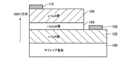
InGaN/GaN系材料を用いたLEDは、例えば図8に示すように、サファイア基板100の(0001)c面上に、n型GaN層102、i型InGaN層104、p型GaN層106を順次積層することにより形成されている。n型GaN層102、i型InGaN層104及びp型GaN層106は、(0001)方向が積層方向を向くように配向している。発光層として機能するi型InGaN層104は、発光層内における輻射性キャリア再結合を促進するために、膜厚数nm程度の薄い量子井戸層により形成されている。
For example, as shown in FIG. 8, an LED using an InGaN / GaN-based material includes an n-
LEDで用いられているこのp−i−n構造を基にして太陽電池を形成することを考えた場合、光吸収層となるInGaN層を厚くして太陽光の吸収効率を高めることが求められる。太陽電池の光吸収層としては、膜厚1μm程度のInGaN層を用いることが望ましい。 When considering the formation of a solar cell based on this pin structure used in an LED, it is required to increase the absorption efficiency of sunlight by increasing the thickness of the InGaN layer serving as a light absorption layer. . As the light absorbing layer of the solar cell, it is desirable to use an InGaN layer having a thickness of about 1 μm.
しかしながら、InGaN/GaNヘテロ構造においては、GaNとInGaNとの間の格子定数差が大きいため、GaN層上に成長したInGaN層には結晶歪みが導入される。例えば、GaNとIn0.1Ga0.9Nとの間には1%程度の格子不整合が存在するため、良好な結晶性を保ちつつGaN層上に成長可能なInGaN層の膜厚は、100nm程度に制限される。このため、InGaN層の膜厚を太陽電池の光吸収層に好適な膜厚まで厚膜化することは困難である。 However, since the lattice constant difference between GaN and InGaN is large in the InGaN / GaN heterostructure, crystal strain is introduced into the InGaN layer grown on the GaN layer. For example, since there is a lattice mismatch of about 1% between GaN and In 0.1 Ga 0.9 N, the thickness of the InGaN layer that can be grown on the GaN layer while maintaining good crystallinity is , Limited to about 100 nm. For this reason, it is difficult to increase the thickness of the InGaN layer to a thickness suitable for the light absorption layer of the solar cell.
また、仮にInGaN層を1μm程度の膜厚まで厚膜化できたとしても、太陽電池として十分な特性を得られないことが、本願発明者の検討により初めて明らかとなった。 Moreover, even if the InGaN layer can be thickened to a thickness of about 1 μm, it has been revealed for the first time by the inventor's study that sufficient characteristics as a solar cell cannot be obtained.
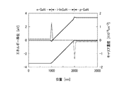
図9は、図8に示すLEDのp−i−n構造においてInGaN層の膜厚を1μmとしたときの伝導帯及び価電子帯のバンド構造を計算により求めた結果を示すグラフである。図中、実線がエネルギー準位を表し、点線がキャリア濃度(電子)を表し、一点鎖線がキャリア濃度(正孔)を表している。計算に当たっては、InGaNのIn組成は0.1とし、p型GaN及びn型GaNの不純物濃度はともに1×1018cm−3とした。図では、左側が表面側であり、右側が基板側である。 FIG. 9 is a graph showing results obtained by calculation of the band structures of the conduction band and the valence band when the film thickness of the InGaN layer is 1 μm in the pin structure of the LED shown in FIG. In the figure, the solid line represents the energy level, the dotted line represents the carrier concentration (electrons), and the alternate long and short dash line represents the carrier concentration (holes). In the calculation, the In composition of InGaN was 0.1, and the impurity concentrations of p-type GaN and n-type GaN were both 1 × 10 18 cm −3 . In the figure, the left side is the surface side, and the right side is the substrate side.
図9に示すように、p型GaN層及びn型GaN層の不純物濃度をともに十分に高くしているにもかかわらず、InGaN層のバンドが、p−n層の傾斜とは反対向きに大きく傾斜している。この結果、光吸収によって生成されたキャリアのうち、電子はp型GaN/InGaN界面に、正孔はInGaN/n型GaN界面に、それぞれ閉じ込められてしまい、いずれのキャリアも電極側に引き抜けない構造になることが判明した。この現象は、本願発明者による更なる検討の結果、窒化物半導体特有の強い分極によって引き起こされる(0001)方向に発生した大きな内部電界が厚いInGaN層の全体に印加されたことで、バンドのトータルの傾斜量が大きくなったためであることが判明した。 As shown in FIG. 9, the band of the InGaN layer is large in the direction opposite to the inclination of the pn layer, although both the impurity concentrations of the p-type GaN layer and the n-type GaN layer are sufficiently high. Inclined. As a result, among the carriers generated by light absorption, electrons are confined at the p-type GaN / InGaN interface and holes are confined at the InGaN / n-type GaN interface, and neither carrier is pulled out to the electrode side. It turned out to be a structure. As a result of further studies by the inventors of the present application, this phenomenon is caused by the fact that a large internal electric field generated in the (0001) direction caused by the strong polarization peculiar to the nitride semiconductor is applied to the entire thick InGaN layer, so that It was found that this was because the amount of inclination of became larger.
このような観点から、本実施形態による太陽電池では、n型GaN/i型InGaN/p型GaNの積層構造を直径数百nm程度以下の柱状構造体30とするとともに、基板側から順に、p型GaN層34、i型InGaN層36及びn型GaN層38を積層している。なお、本実施形態による太陽電池の柱状構造体30のようなナノサイズ(1nm〜数百nm程度)の柱状体は、ナノワイヤと呼ばれることもある。
From such a viewpoint, in the solar cell according to the present embodiment, the stacked structure of n-type GaN / i-type InGaN / p-type GaN is a
n型GaN層38/i型InGaN層36/p型GaN層34の積層構造を柱状構造体30により形成することで、異種材料接合部の断面積を小さくすることができる。これにより、InGaN/GaNのような歪み系材料でも良好な結晶性を維持しつつ厚膜化することが可能となる。
By forming the stacked structure of the n-
例えば、InGaN層36の組成がIn0.10Ga0.90Nの場合、GaNに対する格子不整合は1%程度である。歪み1%の材料系に対しては、半径が200nm、つまり直径が400nm程度が上限となる(例えば非特許文献1を参照)。この場合、n型GaN層38/i型InGaN層36/p型GaN層34の積層構造を直径400nm程度以下の柱状構造体30により形成することにより、良好な結晶性を維持しつつ、太陽電池に好適な膜厚までi−InGaN層36を厚膜化することができる。
For example, when the composition of the
また、基板側から順に、p型GaN層34、i型InGaN層36及びn型GaN層38を積層することにより、バンド構造上も太陽電池にとって好適となる。
Further, by stacking the p-
図2は、本実施形態による太陽電池の伝導帯及び価電子帯のバンド構造を計算により求めた結果を示すグラフである。図中、実線がエネルギー準位を表し、点線がキャリア濃度(電子)を表し、一点鎖線がキャリア濃度(正孔)を表している。計算に当たっては、InGaNのIn組成は0.1とし、p型GaN及びn型GaNの不純物濃度はともに1×1018cm−3とした。図では、左側が表面側であり、右側が基板側である。 FIG. 2 is a graph showing the results of calculating the conduction band and valence band structures of the solar cell according to the present embodiment. In the figure, the solid line represents the energy level, the dotted line represents the carrier concentration (electrons), and the alternate long and short dash line represents the carrier concentration (holes). In the calculation, the In composition of InGaN was 0.1, and the impurity concentrations of p-type GaN and n-type GaN were both 1 × 10 18 cm −3 . In the figure, the left side is the surface side, and the right side is the substrate side.
図2に示すように、基板側から順に、p型GaN層34、i型InGaN層36及びn型GaN層38を積層することにより、p−n構造で傾斜するi型InGaN層36の向きと、i型InGaN層36の内部電界によって傾斜する向きとを一致させることができる。これは、i型InGaN層36の内部電界の向きは、i型InGaN層36の成長する方向に対して常に一定になるからである。これにより、n型GaN/InGaN界面及びInGaN/p型GaN界面におけるキャリアの閉じ込めが生じることなく、光電流を効率的に取り出すことができる。
As shown in FIG. 2, by sequentially stacking a p-
なお、上述のInGaN/GaN系材料を用いたLEDにおいて、n型GaN層102を基板側に配置し、p型GaN層106を表面側に配置しているのは、より良質の積層構造が得られるからである。すなわち、GaNではn型不純物のドーピングは比較的容易であり良質のn型GaNを得ることができるが、p型GaNではn型GaNと比較して結晶性が劣る。n型GaNを基板側に配置して積層構造を形成することにより、p型GaNを基板側に配置にして積層構造を形成する場合と比較して、良質の結晶をエピタキシャル成長することができる。LEDでは、InGaN層の膜厚は数nm程度であり、内部電界による影響もほとんどない。
In the LED using the above-described InGaN / GaN-based material, the n-
この点、本実施形態による太陽電池では、n型GaN層38/i型InGaN層36/p型GaN層34の積層構造を柱状構造体30により形成しているため、p型GaNを基板側に配置した場合にも、良質の結晶をエピタキシャル成長することができる。p型GaNを基板側に配置することで、光電流を効率的に取り出すことも可能となる。
In this regard, in the solar cell according to the present embodiment, since the stacked structure of the n-
また、p型GaN層34を基板側に配置することには、p側電極の形成に適した半導体積層構造を形成するうえでも効果がある。
In addition, disposing the p-
InGaN/GaN系材料を用いたp−i−n構造においては、p型GaN−金属電極間のコンタクト抵抗が、n型GaN−金属電極間のコンタクト抵抗よりも桁で大きく、その分は抵抗損失となってしまうため、低コンタクト抵抗の電極構造である方が望ましい。 In a pin structure using an InGaN / GaN-based material, the contact resistance between the p-type GaN and the metal electrode is orders of magnitude greater than the contact resistance between the n-type GaN and the metal electrode, and the corresponding amount is the resistance loss. Therefore, it is desirable that the electrode structure has a low contact resistance.
一方、GaNは、GaAsやSiなどのバンドギャップエネルギーの小さいIII−V族やIV族半導体材料に対しては、良好なp型コンタクトを形成することが可能である。平板基板上への薄膜成長においてはGaN/GaAsやGaN/Si等の積層構造は歪みの観点から良好な結晶性を保って形成することは難しいが、柱状構造とすることでこのような積層構造も可能となり、低抵抗電極構造を取り入れることが可能となる。 On the other hand, GaN can form a good p-type contact for III-V group and IV group semiconductor materials having a small band gap energy such as GaAs and Si. In thin film growth on a flat substrate, it is difficult to form a laminated structure such as GaN / GaAs or GaN / Si while maintaining good crystallinity from the viewpoint of strain. And a low-resistance electrode structure can be incorporated.
すなわち、p型GaN層34の下地に、金属的伝導性を有するGaAsやSi等よりなるp型半導体層32を配置することで、p型GaN層34とp側電極48との間のコンタクト抵抗を大幅に低減することができる。なお、GaAsやSiは、青色から紫外域の光を吸収するが、p型半導体層32は光の入射方向とは反対の基板側に配置されるため、光電変換効率を阻害することはない。p型半導体層32は、半導体基板10とp型GaN層34との間に求められるコンタクト抵抗の値に応じて適宜形成すればよく、必ずしも形成する必要はない。
That is, the contact resistance between the p-
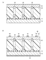
次に、本実施形態による太陽電池の製造方法について図3及び図4を用いて説明する。 Next, the method for manufacturing the solar cell according to the present embodiment will be explained with reference to FIGS.
まず、p型の半導体基板10上に、例えばCVD法により、絶縁膜12を形成する。半導体基板10は、その上に(0001)方向に配向したGaN層及びInGaN層を成長しうるものであればよく、例えば、p型のGaAs(111)B基板を適用することができる。半導体基板10のアクセプタ濃度は、例えば、5×1017cm−3〜1×1019cm−3程度であればよい。また、絶縁膜12は、その後の薄膜成長の際にマスクとなるものであればよく、例えば、シリコン酸化膜を適用することができる。
First, the insulating
次いで、フォトリソグラフィ及びエッチングにより、絶縁膜12に、柱状構造体30の形成予定領域を露出する開口部14を形成する(図3(a))。
Next, an
次いで、絶縁膜12をマスクとして、開口部14内の半導体基板10上に、例えばMOVPE(有機金属気相成長)法により、p型半導体層32、p型GaN層34、i型InGaN層36及びn型GaN層38を順次成長し、柱状構造体30を形成する(図3(b))。
Next, with the insulating
各層の膜厚は、特に限定されるものではないが、例えば、p型半導体層32を100nm、p型GaN層34を300nm、i型InGaN層36を1000nm、n型GaN層38を300nmとする。p型GaN層34、i型InGaN層36及びn型GaN層38は、各層の結晶の(0001)方向が柱状構造体30の積層方向(図面において上方向)を向くように配向成長する。
The thickness of each layer is not particularly limited. For example, the p-
p型半導体層32は、半導体基板10とp型GaN層34との間のコンタクト抵抗を低減するための層であり、例えば、金属的伝導性を有するp型GaAs層やp型Si層により形成する。なお、p型半導体層32は、半導体基板10とp型GaN層34との間に求められるコンタクト抵抗の値に応じて適宜形成すればよく、必ずしも形成する必要はない。
The p-
i型InGaN層36のIn組成は、所望の膜厚のInGaN層36をエピタキシャル成長できる範囲で、太陽電池に求められる吸収端波長に応じて、適宜選択することが望ましく、例えば、0.05〜0.15の範囲とする。なお、In0.05Ga0.95Nの吸収端波長は363nm(3.42eV)であり、In0.10Ga0.90Nの吸収端波長は388nm(3.20eV)であり、In0.15Ga0.85Nの吸収端波長は442nm(2.81eV)である。
The In composition of the i-
GaAs、GaN及びInGaNのGa原料としては、例えば、トリメチルガリウム(TMGa)を用いることができる。GaAsのAs原料としては、例えば、アルシン(AsH3)を用いることができる。GaN及びInGaNの窒素原料としては、例えば、アンモニア(NH3)を用いることができる。InGaNのIn原料としては、例えば、トリメチルインジウム(TMI)を用いることができる。 For example, trimethylgallium (TMGa) can be used as a Ga material for GaAs, GaN, and InGaN. For example, arsine (AsH 3 ) can be used as the GaAs As raw material. As a nitrogen raw material of GaN and InGaN, for example, ammonia (NH 3 ) can be used. As an In raw material of InGaN, for example, trimethylindium (TMI) can be used.
p型のドーパントとしては、GaAsに対しては例えば亜鉛(Zn)を、GaNに対しては例えばマグネシウム(Mg)を用いることができる。Znの原料としては、例えば、ジエチル亜鉛(DEZn)を用いることができる。Mgの原料としては、例えば、ビスシクロペンタジエニルマグネシウム(Cp2Mg)を用いることができる。p型不純物濃度は、例えば、5×1017cm−3〜1×1019cm−3程度であればよい。 As the p-type dopant, for example, zinc (Zn) can be used for GaAs, and for example, magnesium (Mg) can be used for GaN. As a raw material for Zn, for example, diethyl zinc (DEZn) can be used. As a raw material of Mg, for example, biscyclopentadienyl magnesium (Cp2Mg) can be used. The p-type impurity concentration may be, for example, about 5 × 10 17 cm −3 to 1 × 10 19 cm −3 .
n型のドーパントとしては、例えば、シリコン(Si)を用いることができる。Siの原料としては、例えば、ジシラン(Si2H6)を用いることができる。n型不純物濃度は、例えば、5×1017cm−3〜1×1019cm−3程度であればよい。 For example, silicon (Si) can be used as the n-type dopant. As a Si raw material, for example, disilane (Si 2 H 6 ) can be used. The n-type impurity concentration may be, for example, about 5 × 10 17 cm −3 to 1 × 10 19 cm −3 .
柱状構造体30の直径は、歪み材料に対して良好な結晶成長が行えるサイズを上限とする。例えば、InGaN層36の組成がIn0.10Ga0.90Nの場合、GaNに対する格子不整合は1%程度である。歪み1%の材料系に対しては、半径が200nm、つまり直径が400nm程度が上限となる(例えば非特許文献1を参照)。
The diameter of the
一方、柱状構造体30の好適な直径d(nm)の値は、吸収光波長をλ(nm)、屈折率をnとすると、吸収光波長λと、光学距離に換算した柱状構造体30の直径n×dとが等しいときが下限となる。InGaNの吸収波長付近における屈折率nは約3.2であるから、吸収光波長λが400nmであると仮定すると、
d=λ/n=400/3.2=125(nm)
となる。
On the other hand, the preferable value of the diameter d (nm) of the
d = λ / n = 400 / 3.2 = 125 (nm)
It becomes.
次いで、例えばスピンコート法により、柱状構造体30のn型GaN層38部分が露出するように、透明な樹脂を塗布し、樹脂層40を形成する(図3(c))。
Next, a transparent resin is applied by, for example, spin coating so that the n-
次いで、n型GaN層38及び樹脂層40上に、例えばITO等の透明導電膜を堆積し、透明電極42を形成する(図4(a))。
Next, a transparent conductive film such as ITO is deposited on the n-
次いで、透明電極44上に、グリッド状の金属グリッド電極44を形成し、透明電極42及び金属電極44よりなるn側電極46を形成する。また、半導体基板10の裏面に、p側電極48を形成する(図4(b))。
Next, a grid-like
こうして、本実施形態による太陽電池を完成する。 Thus, the solar cell according to the present embodiment is completed.
このように、本実施形態によれば、n型GaN/i型InGaN/p型GaNの積層構造を柱状構造体により形成するので、良好な結晶性を維持しつつ光吸収層であるi型InGaNを厚膜化することができる。また、基板側から順に、p型GaN層、i型InGaN層及びn型GaN層を積層するので、n型GaN/InGaN界面及びInGaN/p型GaN界面におけるキャリアの閉じ込めを防止することができる。これにより、光吸収層における光吸収効率を向上するとともに光電流を効率的に取り出すことができ、高効率の太陽電池を実現することができる。 As described above, according to the present embodiment, since the stacked structure of n-type GaN / i-type InGaN / p-type GaN is formed by the columnar structure, i-type InGaN that is a light absorption layer while maintaining good crystallinity. Can be thickened. In addition, since the p-type GaN layer, the i-type InGaN layer, and the n-type GaN layer are stacked in this order from the substrate side, carrier confinement at the n-type GaN / InGaN interface and the InGaN / p-type GaN interface can be prevented. Thereby, while improving the light absorption efficiency in a light absorption layer, a photocurrent can be taken out efficiently and a highly efficient solar cell can be implement | achieved.
[第2実施形態]
第2実施形態による太陽電池及びその製造方法について図5乃至図7を用いて説明する。図1乃至図4に示す第1実施形態による太陽電池及びその製造方法と同様の構成要素には同一の符号を付し説明を省略し又は簡潔にする。
[Second Embodiment]
A solar cell and a method for manufacturing the solar cell according to the second embodiment will be described with reference to FIGS. Components similar to those of the solar cell and the manufacturing method thereof according to the first embodiment shown in FIGS. 1 to 4 are denoted by the same reference numerals, and description thereof is omitted or simplified.
図5は、本実施形態による太陽電池の構造を示す概略断面図である。図6及び図7は、本実施形態による太陽電池の製造方法を示す工程断面図である。 FIG. 5 is a schematic cross-sectional view showing the structure of the solar cell according to the present embodiment. 6 and 7 are process cross-sectional views illustrating the method for manufacturing the solar cell according to the present embodiment.
はじめに、本実施形態による太陽電池の構造について図5を用いて説明する。 First, the structure of the solar cell according to the present embodiment will be described with reference to FIG.
p型の半導体基板20上には、柱状導電体30が形成されている。柱状導電体30は、半導体基板10側から、p型半導体層32と、p型GaN層34と、i型InGaN層36と、n型GaN層38とが順次積層された積層構造を有している。p型GaN層34、i型InGaN層36及びn型GaN層38は、各層の結晶の(0001)方向が柱状構造体30の積層方向(図面において上方向)を向くように配向している。
A
柱状構造体30が形成された領域を除く半導体基板20上には、絶縁膜12が形成されている。絶縁膜12上に突出する柱状構造体30の側壁部分には、樹脂層40が形成されている。柱状構造体30の頭頂部のn型GaN層38の少なくとも一部は、樹脂層40から露出している。
An insulating
樹脂層40上及び樹脂層40から露出するn型GaN層38上には、n側電極46が形成されている。また、半導体基板20の裏面の柱状構造体30間の領域には、グリッド状のp側電極48が形成されている。
An n-
第1実施形態による太陽電池はn側電極46側を太陽光に向けて使用するタイプの太陽電池であるのに対し、本実施形態による太陽電池はp側電極48側を太陽光に向けて使用するタイプの太陽電池である。
The solar cell according to the first embodiment is a type of solar cell that uses the n-
このような観点から、本実施形態による太陽電池の半導体基板20としては、その上に(0001)方向に配向したGaN層及びInGaN層を成長することができ、且つ、青色から紫外域の光を吸収しない材料の半導体基板を用いる。このような半導体基板20としては、例えば、p型の(111)SiC基板を適用することができる。
From such a viewpoint, as the
p型半導体層32は、半導体基板20とp型GaN層34との間のコンタクト抵抗を低減するための層であり、例えば、金属的伝導性を有するp型GaP層を適用することができる。なお、p型半導体層32による光吸収が懸念される場合には、p型半導体層32を薄くし或いは省略してもよい。
The p-
本実施形態による太陽電池は、半導体基板20の裏面側を太陽光に向けて使用するため、半導体基板20の裏面側に配置するp側電極48をグリッド状とする。半導体基板20の表面側の透明電極42は不要である。
Since the solar cell according to the present embodiment uses the back surface side of the
次に、本実施形態による太陽電池の製造方法について図6及び図7を用いて説明する。 Next, the method for manufacturing the solar cell according to the present embodiment will be explained with reference to FIGS.
まず、図3(a)に示す第1実施形態による太陽電池の製造法と同様にして、p型の半導体基板20上に、柱状構造体30の形成予定領域を露出する開口部14を有する絶縁膜12を形成する。半導体基板20は、その上に(0001)方向に配向したGaN層及びInGaN層を成長することができ、且つ、青色から紫外域の光を吸収しない材料であればよく、例えば、p型のSiC(111)基板を適用することができる。半導体基板20のアクセプタ濃度は、例えば、5×1017cm−3〜1×1019cm−3程度であればよい。
First, in the same manner as in the method for manufacturing the solar cell according to the first embodiment shown in FIG. 3A, an insulation having an
次いで、絶縁膜12をマスクとして、開口部14内の半導体基板20上に、例えばMOVPE法により、p型半導体層32、p型GaN層34、i型InGaN層36及びn型GaN層38を順次成長し、柱状構造体30を形成する(図6(a))。
Next, using the insulating
各層の膜厚は、特に限定されるものではないが、例えば、p型半導体層32を100nm、p型GaN層34を300nm、i型InGaN層36を1000nm、n型GaN層38を300nmとする。p型GaN層34、i型InGaN層36及びn型GaN層38は、各層の結晶の(0001)方向が柱状構造体30の積層方向(図面において上方向)を向くように配向成長する。
The thickness of each layer is not particularly limited. For example, the p-
p型半導体層32は、半導体基板10とp型GaN層34との間のコンタクト抵抗を低減するための層であり、例えば、金属的伝導性を有するp型GaP層により形成する。なお、p型半導体層32は、必ずしも形成する必要はない。
The p-
次いで、例えばスピンコート法により、柱状構造体30のn型GaN層38部分が露出するように、透明な樹脂を塗布し、樹脂層40を形成する(図6(b))。
Next, a transparent resin is applied by, for example, spin coating so that the n-
次いで、n型GaN層38及び樹脂層40上に、n側電極46を形成する(図7(a))。また、半導体基板20の裏面に、グリッド状のp側電極48を形成する(図7(b))。
Next, an n-
こうして、本実施形態による太陽電池を完成する。 Thus, the solar cell according to the present embodiment is completed.
このように、本実施形態によれば、n型GaN/i型InGaN/p型GaNの積層構造を柱状構造体により形成するので、良好な結晶性を維持しつつ光吸収層であるi型InGaNを厚膜化することができる。また、基板側から順に、p型GaN層、i型InGaN層及びn型GaN層を積層するので、n型GaN/InGaN界面及びInGaN/p型GaN界面におけるキャリアの閉じ込めを防止することができる。これにより、光吸収層における光吸収効率を向上するとともに光電流を効率的に取り出すことができ、高効率の太陽電池を実現することができる。 As described above, according to the present embodiment, since the stacked structure of n-type GaN / i-type InGaN / p-type GaN is formed by the columnar structure, i-type InGaN that is a light absorption layer while maintaining good crystallinity. Can be thickened. In addition, since the p-type GaN layer, the i-type InGaN layer, and the n-type GaN layer are stacked in this order from the substrate side, carrier confinement at the n-type GaN / InGaN interface and the InGaN / p-type GaN interface can be prevented. Thereby, while improving the light absorption efficiency in a light absorption layer, a photocurrent can be taken out efficiently and a highly efficient solar cell can be implement | achieved.
[変形実施形態]
上記実施形態に限らず種々の変形が可能である。
[Modified Embodiment]
The present invention is not limited to the above embodiment, and various modifications are possible.
例えば、上記実施形態では、柱状構造体30の断面形状について特に記載していないが、円形や多角形などの対称な形状だけでなく、楕円形状などの形状としてもよい。
For example, in the above embodiment, the cross-sectional shape of the
また、上記実施形態では、太さが一定の柱状構造体30を示したが、柱状構造体30の太さは必ずしも一定である必要はない。例えば、半導体基板10/20側から離間するにつれて太さが徐々に狭まる錐台形状の柱状構造体としてもよい。
Moreover, in the said embodiment, although the
また、上記実施形態に記載した太陽電池の構造、構成材料、製造条件等は、一例を示したものにすぎず、当業者の技術常識等に応じて適宜修正や変更が可能である。 In addition, the structure, constituent materials, manufacturing conditions, and the like of the solar cell described in the above embodiment are merely examples, and can be appropriately modified or changed according to technical common sense of those skilled in the art.
10,20…半導体基板
12…絶縁膜
14…開口部
30…柱状構造体
32…p型半導体層
34…p型GaN層
36…i型InGaN層
38…n型GaN層
40…樹脂層
42…透明電極
44…金属グリッド電極
46…n側電極
48…p側電極
100…サファイア基板
102…n型GaN層
104…i型InGaN層
106…p型GaN層
108…n側電極
110…p側電極
DESCRIPTION OF
Claims (8)
前記半導体基板上に形成されたp型GaN層と、前記p型GaN層上に形成されたInGaN光吸収層と、前記InGaN光吸収層上に形成されたn型GaN層とを有する柱状構造体と、
前記半導体基板と前記p型GaN層との間に形成され、金属的伝導性を有するp型GaAs層又はp型Si層のp型半導体層と
を有することを特徴とする太陽電池。 a p-type semiconductor substrate;
A columnar structure having a p-type GaN layer formed on the semiconductor substrate, an InGaN light absorption layer formed on the p-type GaN layer, and an n-type GaN layer formed on the InGaN light absorption layer When,
A solar cell comprising a p-type GaAs layer or a p-type Si layer of a p-type Si layer formed between the semiconductor substrate and the p-type GaN layer and having metallic conductivity.
前記半導体基板上に形成されたp型GaN層と、前記p型GaN層上に形成されたInGaN光吸収層と、前記InGaN光吸収層上に形成されたn型GaN層とを有する柱状構造体と、
前記半導体基板と前記p型GaN層との間に形成され、金属的伝導性を有するp型GaP層のp型半導体層と
を有することを特徴とする太陽電池。 a p-type semiconductor substrate;
A columnar structure having a p-type GaN layer formed on the semiconductor substrate, an InGaN light absorption layer formed on the p-type GaN layer, and an n-type GaN layer formed on the InGaN light absorption layer When,
A solar cell comprising: a p-type semiconductor layer of a p-type GaP layer formed between the semiconductor substrate and the p-type GaN layer and having metallic conductivity.
前記p型GaN層、前記InGaN光吸収層及び前記n型GaN層は、(0001)方向に配向している
ことを特徴とする太陽電池。 The solar cell according to claim 1 or 2,
The p-type GaN layer, the InGaN light absorption layer, and the n-type GaN layer are oriented in the (0001) direction.
前記半導体基板は、GaAs(111)基板である
ことを特徴とする太陽電池。 In claim 1 Symbol placement of the solar cell,
The solar cell is characterized in that the semiconductor substrate is a GaAs (111) substrate.
前記半導体基板は、SiC(111)基板である
ことを特徴とする太陽電池。 The solar cell according to claim 2,
The said semiconductor substrate is a SiC (111) substrate. The solar cell characterized by the above-mentioned.
前記柱状構造体の直径は、125nm〜400nmである
ことを特徴とする太陽電池。 The solar cell according to any one of claims 1 to 5,
The columnar structure has a diameter of 125 nm to 400 nm.
前記半導体基板に接続されたp側電極と、
前記n型GaN層に接続されたn側電極と
を更に有することを特徴とする太陽電池。 The solar cell according to any one of claims 1 to 6,
A p-side electrode connected to the semiconductor substrate;
And a n-side electrode connected to the n-type GaN layer.
前記マスク膜をマスクとして、前記開口部内の前記半導体基板上に、p型GaN層と、InGaN光吸収層と、n型GaN層とを(0001)方向に配向して順次成長し、前記p型GaN層、前記InGaN光吸収層及び前記n型GaN層の積層構造を有する柱状構造体を形成する工程と
を有することを特徴とする太陽電池の製造方法。 forming a mask film having an opening on a p-type semiconductor substrate;
Using the mask film as a mask, a p-type GaN layer, an InGaN light absorption layer, and an n-type GaN layer are sequentially grown in the (0001) direction on the semiconductor substrate in the opening, and the p-type is grown. Forming a columnar structure having a laminated structure of a GaN layer, the InGaN light absorption layer, and the n-type GaN layer.
Priority Applications (1)
| Application Number | Priority Date | Filing Date | Title |
|---|---|---|---|
| JP2012259941A JP6060652B2 (en) | 2012-11-28 | 2012-11-28 | Solar cell and manufacturing method thereof |
Applications Claiming Priority (1)
| Application Number | Priority Date | Filing Date | Title |
|---|---|---|---|
| JP2012259941A JP6060652B2 (en) | 2012-11-28 | 2012-11-28 | Solar cell and manufacturing method thereof |
Publications (2)
| Publication Number | Publication Date |
|---|---|
| JP2014107441A JP2014107441A (en) | 2014-06-09 |
| JP6060652B2 true JP6060652B2 (en) | 2017-01-18 |
Family
ID=51028667
Family Applications (1)
| Application Number | Title | Priority Date | Filing Date |
|---|---|---|---|
| JP2012259941A Expired - Fee Related JP6060652B2 (en) | 2012-11-28 | 2012-11-28 | Solar cell and manufacturing method thereof |
Country Status (1)
| Country | Link |
|---|---|
| JP (1) | JP6060652B2 (en) |
Cited By (5)
| Publication number | Priority date | Publication date | Assignee | Title |
|---|---|---|---|---|
| US10502435B2 (en) | 2013-09-06 | 2019-12-10 | Zinniatek Limited | Solar thermal roofing system |
| US10858839B2 (en) | 2011-11-30 | 2020-12-08 | Zinniatek Limited | Roofing, cladding or siding product, its manufacture and its use as part of a solar energy recovery system |
| US11011912B2 (en) | 2011-11-30 | 2021-05-18 | Zinniatek Limited | Photovoltaic systems |
| US11408613B2 (en) | 2014-03-07 | 2022-08-09 | Zinniatek Limited | Solar thermal roofing system |
| US11970858B2 (en) | 2017-02-21 | 2024-04-30 | Zinniatek Limited | Substrate having decorated surface and method of production |
Family Cites Families (15)
| Publication number | Priority date | Publication date | Assignee | Title |
|---|---|---|---|---|
| JP3332127B2 (en) * | 1995-03-20 | 2002-10-07 | 株式会社東芝 | Semiconductor element |
| JP3955367B2 (en) * | 1997-09-30 | 2007-08-08 | フィリップス ルミレッズ ライティング カンパニー リミテッド ライアビリティ カンパニー | Optical semiconductor device and manufacturing method thereof |
| JP2000277440A (en) * | 1999-03-25 | 2000-10-06 | Nec Corp | Nitride iii-v compound semiconductor crystal film, semiconductor device, and semiconductor laser using the same |
| JP3702700B2 (en) * | 1999-03-31 | 2005-10-05 | 豊田合成株式会社 | Group III nitride compound semiconductor device and method for manufacturing the same |
| JP4104305B2 (en) * | 2001-08-07 | 2008-06-18 | 三洋電機株式会社 | Nitride semiconductor chip and nitride semiconductor substrate |
| JP4118061B2 (en) * | 2002-02-07 | 2008-07-16 | 三洋電機株式会社 | Semiconductor forming method and semiconductor element |
| JP2003318434A (en) * | 2002-04-25 | 2003-11-07 | Nichia Chem Ind Ltd | Nitride semiconductor light receiving element and method of manufacturing the same |
| US20060207647A1 (en) * | 2005-03-16 | 2006-09-21 | General Electric Company | High efficiency inorganic nanorod-enhanced photovoltaic devices |
| EP1949451A4 (en) * | 2005-08-22 | 2016-07-20 | Q1 Nanosystems Inc | Nanostructure and photovoltaic cell implementing same |
| US7629532B2 (en) * | 2006-12-29 | 2009-12-08 | Sundiode, Inc. | Solar cell having active region with nanostructures having energy wells |
| US8183566B2 (en) * | 2007-03-01 | 2012-05-22 | Hewlett-Packard Development Company, L.P. | Hetero-crystalline semiconductor device and method of making same |
| US9224595B2 (en) * | 2008-09-01 | 2015-12-29 | Sophia School Corporation | Semiconductor optical element array and method of manufacturing the same |
| US20110115041A1 (en) * | 2009-11-19 | 2011-05-19 | Zena Technologies, Inc. | Nanowire core-shell light pipes |
| US20100148221A1 (en) * | 2008-11-13 | 2010-06-17 | Zena Technologies, Inc. | Vertical photogate (vpg) pixel structure with nanowires |
| JP2012188294A (en) * | 2011-03-08 | 2012-10-04 | Tohoku Univ | Method for manufacturing semiconductor device |
-
2012
- 2012-11-28 JP JP2012259941A patent/JP6060652B2/en not_active Expired - Fee Related
Cited By (5)
| Publication number | Priority date | Publication date | Assignee | Title |
|---|---|---|---|---|
| US10858839B2 (en) | 2011-11-30 | 2020-12-08 | Zinniatek Limited | Roofing, cladding or siding product, its manufacture and its use as part of a solar energy recovery system |
| US11011912B2 (en) | 2011-11-30 | 2021-05-18 | Zinniatek Limited | Photovoltaic systems |
| US10502435B2 (en) | 2013-09-06 | 2019-12-10 | Zinniatek Limited | Solar thermal roofing system |
| US11408613B2 (en) | 2014-03-07 | 2022-08-09 | Zinniatek Limited | Solar thermal roofing system |
| US11970858B2 (en) | 2017-02-21 | 2024-04-30 | Zinniatek Limited | Substrate having decorated surface and method of production |
Also Published As
| Publication number | Publication date |
|---|---|
| JP2014107441A (en) | 2014-06-09 |
Similar Documents
| Publication | Publication Date | Title |
|---|---|---|
| US10050166B2 (en) | Silicon heterojunction photovoltaic device with wide band gap emitter | |
| JP3657143B2 (en) | Solar cell and manufacturing method thereof | |
| US8952243B2 (en) | Stacked structure including vertically grown semiconductor, p-n junction device including the stacked structure, and method of manufacturing thereof | |
| US11271133B2 (en) | Multi-junction optoelectronic device with group IV semiconductor as a bottom junction | |
| US9324911B2 (en) | Methods of fabricating dilute nitride semiconductor materials for use in photoactive devices and related structures | |
| JP6060652B2 (en) | Solar cell and manufacturing method thereof | |
| JP2020513167A (en) | Nano structure | |
| US20160056333A1 (en) | Nitride semiconductor multilayer film reflector and light-emitting device using the same | |
| JP2010267934A (en) | Solar cell, and method of manufacturing the same | |
| US9337377B2 (en) | Methods of forming dilute nitride materials for use in photoactive devices and related structures | |
| JP2006128527A (en) | Method of manufacturing garium nitride system compound semiconductor | |
| US20180287015A1 (en) | Semiconductor device | |
| JP6335784B2 (en) | Variable band gap solar cell | |
| TWI496314B (en) | Compound semiconductor solar cell manufacturing laminated body, compound semiconductor solar cell and manufacturing method thereof | |
| US20150122329A1 (en) | Silicon heterojunction photovoltaic device with non-crystalline wide band gap emitter | |
| JP5283588B2 (en) | Solar cell | |
| Yu et al. | Conversion efficiency improvement of InGaN/GaN multiple-quantum-well solar cells with ex situ AlN nucleation layer | |
| CN108269866B (en) | Mixed polarity InGaN solar cell structure | |
| JP5634955B2 (en) | III-V compound semiconductor film manufacturing method and compound semiconductor solar cell manufacturing method | |
| KR101539183B1 (en) | Polyhedron having upper width narrower than lower width, method for fabricating the same, and photoelectric conversion device having the same | |
| JP2013197485A (en) | Epitaxial substrate and semiconductor element manufacturing method using the same | |
| US10763111B2 (en) | Polyhedron of which upper width is narrower than lower width, manufacturing method therefor, and photoelectric conversion device comprising same | |
| CN108198893A (en) | A kind of nitrogen face polar InGaN solar battery structures | |
| JP2013183125A (en) | Compound semiconductor device epitaxial growth substrate | |
| JP2011222620A (en) | Solar cell |
Legal Events
| Date | Code | Title | Description |
|---|---|---|---|
| A621 | Written request for application examination |
Free format text: JAPANESE INTERMEDIATE CODE: A621 Effective date: 20150706 |
|
| A977 | Report on retrieval |
Free format text: JAPANESE INTERMEDIATE CODE: A971007 Effective date: 20160229 |
|
| A131 | Notification of reasons for refusal |
Free format text: JAPANESE INTERMEDIATE CODE: A131 Effective date: 20160308 |
|
| A521 | Request for written amendment filed |
Free format text: JAPANESE INTERMEDIATE CODE: A523 Effective date: 20160506 |
|
| A131 | Notification of reasons for refusal |
Free format text: JAPANESE INTERMEDIATE CODE: A131 Effective date: 20160719 |
|
| A521 | Request for written amendment filed |
Free format text: JAPANESE INTERMEDIATE CODE: A523 Effective date: 20160906 |
|
| TRDD | Decision of grant or rejection written | ||
| A01 | Written decision to grant a patent or to grant a registration (utility model) |
Free format text: JAPANESE INTERMEDIATE CODE: A01 Effective date: 20161115 |
|
| A61 | First payment of annual fees (during grant procedure) |
Free format text: JAPANESE INTERMEDIATE CODE: A61 Effective date: 20161128 |
|
| R150 | Certificate of patent or registration of utility model |
Ref document number: 6060652 Country of ref document: JP Free format text: JAPANESE INTERMEDIATE CODE: R150 |
|
| LAPS | Cancellation because of no payment of annual fees |