JP6058640B2 - Production equipment for producing patterned layers - Google Patents
Production equipment for producing patterned layers Download PDFInfo
- Publication number
- JP6058640B2 JP6058640B2 JP2014511980A JP2014511980A JP6058640B2 JP 6058640 B2 JP6058640 B2 JP 6058640B2 JP 2014511980 A JP2014511980 A JP 2014511980A JP 2014511980 A JP2014511980 A JP 2014511980A JP 6058640 B2 JP6058640 B2 JP 6058640B2
- Authority
- JP
- Japan
- Prior art keywords
- layer
- protective material
- substrate
- unit
- patterned
- Prior art date
- Legal status (The legal status is an assumption and is not a legal conclusion. Google has not performed a legal analysis and makes no representation as to the accuracy of the status listed.)
- Expired - Fee Related
Links
Images


Classifications
-
- H—ELECTRICITY
- H10—SEMICONDUCTOR DEVICES; ELECTRIC SOLID-STATE DEVICES NOT OTHERWISE PROVIDED FOR
- H10K—ORGANIC ELECTRIC SOLID-STATE DEVICES
- H10K71/00—Manufacture or treatment specially adapted for the organic devices covered by this subclass
- H10K71/621—Providing a shape to conductive layers, e.g. patterning or selective deposition
-
- H—ELECTRICITY
- H01—ELECTRIC ELEMENTS
- H01L—SEMICONDUCTOR DEVICES NOT COVERED BY CLASS H10
- H01L21/00—Processes or apparatus adapted for the manufacture or treatment of semiconductor or solid state devices or of parts thereof
- H01L21/02—Manufacture or treatment of semiconductor devices or of parts thereof
- H01L21/02104—Forming layers
-
- H—ELECTRICITY
- H10—SEMICONDUCTOR DEVICES; ELECTRIC SOLID-STATE DEVICES NOT OTHERWISE PROVIDED FOR
- H10K—ORGANIC ELECTRIC SOLID-STATE DEVICES
- H10K50/00—Organic light-emitting devices
-
- H—ELECTRICITY
- H10—SEMICONDUCTOR DEVICES; ELECTRIC SOLID-STATE DEVICES NOT OTHERWISE PROVIDED FOR
- H10K—ORGANIC ELECTRIC SOLID-STATE DEVICES
- H10K71/00—Manufacture or treatment specially adapted for the organic devices covered by this subclass
Description
本発明は、パターン化された層を製作するための製作装置、製作方法、及び製作用コンピュータプログラムに関する。本発明は、更に、パターン化された層を有する有機発光ダイオード(OLED)のような電気デバイスに関する。 The present invention relates to a production apparatus, a production method, and a production computer program for producing a patterned layer. The invention further relates to an electrical device such as an organic light emitting diode (OLED) having a patterned layer.
OLEDは、一般に、陽極を提供するパターン化された導電性材料を有し、有機層は、陽極と、陰極を形成する他の導電層との間に挟まれている。陽極を形成する導電層は、一般に、フォトリソグラフィーを使用してパターン化される。フォトリソグラフィーは、フォトリソグラフィーをコストのかかる工程にする、非常に高い精度及び微細解像度のために開発されてきたので、パターン化された層を、特に一連の小さな製品用のパターン化された層を高価な部品にしている。 OLEDs generally have a patterned conductive material that provides the anode, and the organic layer is sandwiched between the anode and other conductive layers that form the cathode. The conductive layer forming the anode is generally patterned using photolithography. Since photolithography has been developed for very high precision and fine resolution, which makes photolithography an expensive process, patterned layers, especially for a series of small products. They are expensive parts.
コストのかかるフォトリソグラフィー工程を使用せずに、パターン化された層を製作するための製作装置、製作方法、及び製作用コンピュータプログラムを提供することが本発明の目的である。製作されたパターン化された層を有するOLEDのような電気デバイスを提供することが本発明の更なる目的である。 It is an object of the present invention to provide a fabrication apparatus, a fabrication method, and a production computer program for fabricating a patterned layer without using a costly photolithography process. It is a further object of the present invention to provide an electrical device such as an OLED having a patterned layer fabricated.
本発明の第1態様では、パターン化された層を基板の上に製作するための製作装置が開示されており、前記基板は、前記層を形成する層材料が付与される第1領域と、前記層材料が付与されない第2領域と、を有し、前記製作装置は、
‐前記基板の上の第2領域に保護材料を付与する保護材料付与ユニットと、
‐前記基板の上の第1領域に液状層材料を印刷する層材料付与ユニットと、
‐前記保護材料の融解温度よりも低い乾燥温度まで、層材料を加熱することによって、層材料を乾燥させる乾燥ユニットと、
‐前記保護材料の融解温度よりも高い除去温度を用いて、基板から保護材料を除去する保護材料除去ユニットと、
を有する。
In a first aspect of the present invention, a fabrication apparatus for fabricating a patterned layer on a substrate is disclosed, the substrate comprising a first region to which a layer material forming the layer is applied; A second region to which the layer material is not applied, and the manufacturing apparatus includes:
A protective material applying unit for applying a protective material to the second region on the substrate;
A layer material application unit for printing a liquid layer material on the first region on the substrate;
A drying unit for drying the layer material by heating the layer material to a drying temperature lower than the melting temperature of the protective material;
A protective material removal unit for removing the protective material from the substrate using a removal temperature higher than the melting temperature of the protective material;
Have
層材料は、基板の上の第1領域に印刷されるので、コストのかかるフォトリソグラフィー工程を使用することなく、パターン化された層を製造することができる。それだけでなく、基板の上の第1領域に液状層材料を印刷する前に、基板の上の第2領域に保護材料が付与されるので、第2領域では、層材料は保護材料の上にのみ位置することができる。従って、保護材料が除去された後、層材料は第1領域にのみ存在し、第2領域には存在しない。これにより、パターン化された層の品質が向上される。 Since the layer material is printed in the first region on the substrate, a patterned layer can be produced without using costly photolithography processes. In addition, since the protective material is applied to the second region on the substrate before printing the liquid layer material on the first region on the substrate, in the second region, the layer material is on the protective material. Can only be located. Thus, after the protective material is removed, the layer material is present only in the first region and not in the second region. This improves the quality of the patterned layer.
パターン化された層は、直接基板の上に位置付けられうる、あるいは、1又は複数の他の層が基板とパターン化された層との間に配置されうる。例えば、前記基板は、酸化シリコン又は窒化シリコンを含むバリア層と、酸化インジウム錫(ITO)被覆のような導電性被覆とで被覆されたガラスプレートでもよい。前記導電性被覆は、好ましくは透明である。製作装置は、従って、保護材料を付与し、基板の上に既に提供された導電層の上に層材料を印刷するのに適しうる。 The patterned layer can be positioned directly on the substrate, or one or more other layers can be placed between the substrate and the patterned layer. For example, the substrate may be a glass plate coated with a barrier layer comprising silicon oxide or silicon nitride and a conductive coating such as an indium tin oxide (ITO) coating. The conductive coating is preferably transparent. The fabrication device can thus be suitable for applying a protective material and printing a layer material on a conductive layer already provided on the substrate.
選択的に1又は複数の被覆を有する基板は、保護材料を付与し、層材料を印刷する前に洗浄されうる。選択的に1又は複数の被覆を有する基板は、保護材料及び/又は層材料の一般に起こりうる広範囲にわたる拡散を減少させる、特に防止するために、印刷精度及びぬれ挙動が改善されるように前処理もされうる。 Optionally, the substrate having one or more coatings can be cleaned before applying the protective material and printing the layer material. The substrate, optionally with one or more coatings, is pretreated so that the printing accuracy and wetting behavior are improved in order to reduce, in particular to prevent, the widespread diffusion of protective materials and / or layer materials in general. It can also be done.
好ましい実施形態では、前記保護材料付与ユニットは、保護材料を印刷することによって付与するのに適している。印刷は、フォトリソグラフィーに比べてコストがかからないという利点を有し、1つのデザインから別のデザインへ速い切り替え時間を提供することができる。更に好ましくは、前記保護材料付与ユニットは、ワックスを保護材料として付与するのに適している。実施形態では、約90℃で液体になるワックスが使用される。前記ワックスは、好ましくは印刷可能なホットワックスインクである。 In a preferred embodiment, the protective material application unit is suitable for applying the protective material by printing. Printing has the advantage of being less costly than photolithography and can provide fast switching times from one design to another. More preferably, the protective material applying unit is suitable for applying wax as a protective material. In an embodiment, a wax is used that becomes liquid at about 90 ° C. The wax is preferably a printable hot wax ink.
前記層材料付与ユニットは、金属を層材料として付与するのに適していることも好ましい。前記層材料は、好ましくは銀又は銅を含む。例えば、前記層材料付与ユニットは、層材料を付与するのにインクジェット印刷又はスクリーン印刷を使用するのに適している。好ましくは、前記層材料付与ユニットは、基板の上の第1領域に金属インクを印刷するのに適している。 It is also preferable that the layer material application unit is suitable for applying metal as a layer material. The layer material preferably comprises silver or copper. For example, the layer material application unit is suitable for using ink jet printing or screen printing to apply the layer material. Preferably, the layer material application unit is suitable for printing metal ink on the first region on the substrate.
前記基板は、好ましくは導電層で被覆され、前記製作装置は、保護材料と、基板の上にパターン化された導電層を生成するために付与された層材料との、少なくとも1つを通して導電層を焼灼する焼灼ユニットを更に有しうる。特に、前記焼灼ユニットは、保護材料及び/又は層材料を通してレーザー焼灼を行うレーザーを有する。実施形態では、前記レーザーは、等しいパルスエネルギーを得るためのQ−スイッチモードを有する355nmで動作する半導体レーザーである。当該ビームプロファイルは、ガウス形状となりうる。しかしながら、好ましい実施形態では、ビームプロファイルは、フラットトップ・プロファイルである。レーザー焼灼も、フォトリソグラフィーよりもコストがかからず、1つのデザインから別のデザインへ速い切り替え時間を提供できる。 The substrate is preferably coated with a conductive layer, and the fabrication device is configured to pass the conductive layer through at least one of a protective material and a layer material applied to produce a patterned conductive layer on the substrate. It may further have a cautery unit for cauterizing. In particular, the ablation unit has a laser that performs laser ablation through the protective material and / or the layer material. In an embodiment, the laser is a semiconductor laser operating at 355 nm with a Q-switch mode to obtain equal pulse energy. The beam profile can be Gaussian. However, in a preferred embodiment, the beam profile is a flat top profile. Laser ablation is also less expensive than photolithography and can provide faster switching times from one design to another.
前記導電層の焼灼は、層材料が付与された後に、特に基板の上に、すなわち基板の導電層の上に金属インクが印刷され乾燥された後に、好ましくは行われる。前記焼灼ユニットは、好ましくは基板の上の導電層としてのITO層を焼灼するのに適している。 The cauterization of the conductive layer is preferably carried out after the layer material has been applied, in particular after the metal ink has been printed and dried on the substrate, ie on the conductive layer of the substrate. The ablation unit is preferably suitable for ablating an ITO layer as a conductive layer on a substrate.
前記保護材料除去ユニットは、保護材料を除去するために加熱された水を使用するのに適していることが更に好ましい。従って、保護材料は、加熱された水を使用するだけという、比較的単純な方法で除去されうる。好ましくは、保護材料、好ましくはワックスは、ワックスの融解温度よりも高い温度まで加熱された水を使用して除去される。前記水は、好ましくは蒸留水である。例えば、水は、ワックスが液体になる温度である約90℃又はより高い温度まで加熱される。水は、例えば100℃以下の温度では液体として、約100℃の温度では蒸気として、あるいは、例えば100℃よりも高い温度では過熱蒸気として、提供されうる。除去処理は、スプレー‐ストリッピング又は他のストリッピング技術によって行われうる。 More preferably, the protective material removal unit is suitable for using heated water to remove the protective material. Thus, the protective material can be removed in a relatively simple manner, using only heated water. Preferably, the protective material, preferably the wax, is removed using water heated to a temperature above the melting temperature of the wax. The water is preferably distilled water. For example, the water is heated to about 90 ° C. or higher, the temperature at which the wax becomes liquid. Water can be provided, for example, as a liquid at temperatures below 100 ° C., as steam at temperatures of about 100 ° C., or as superheated steam at temperatures above, for example, 100 ° C. The removal process can be performed by spray-stripping or other stripping techniques.
前記保護材料除去ユニットは、層構造部、特に基板を保護材料が気化する温度まで加熱するのに更に適しうる。前記気化は、加熱された水のみを使用して行われた除去処理の後でまだ存在しているであろう保護材料の単層を除去しうる。 The protective material removal unit may be further suitable for heating the layer structure, in particular the substrate, to a temperature at which the protective material vaporizes. The vaporization can remove a monolayer of protective material that would still be present after a removal process performed using only heated water.
好ましい実施形態では、前記製作装置は、層材料を焼結するための焼結ユニットを更に有する。層材料は、好ましくは、例えば130℃よりも高い温度で焼結される銀又は銅のような金属インクである。焼結によって、ワックスの可能な限りの残余部分もこれらを気化させることによって除去されうる。 In a preferred embodiment, the production apparatus further comprises a sintering unit for sintering the layer material. The layer material is preferably a metallic ink, such as silver or copper, which is sintered at a temperature higher than 130 ° C., for example. By sintering, as much residual part of the wax as possible can be removed by vaporizing them.
前記製作装置が、保護材料が除去された後に、層材料の上に絶縁材料を付与するための絶縁材料付与ユニットを有することも好ましい。前記絶縁材料付与ユニットは、好ましくはインクジェット印刷によって絶縁材料を付与するのに適している。前記絶縁材料は、好ましくはレジストである。 It is also preferable that the manufacturing apparatus has an insulating material applying unit for applying an insulating material on the layer material after the protective material is removed. The insulating material application unit is suitable for applying an insulating material, preferably by ink jet printing. The insulating material is preferably a resist.
前記製作装置は、絶縁材料を硬化するための硬化ユニットを更に有することができる。実施形態では、前記硬化ユニットは絶縁材料を加熱するのに適している。 The fabrication apparatus can further include a curing unit for curing the insulating material. In an embodiment, the curing unit is suitable for heating the insulating material.
実施形態では、前記製作装置は、パターン化された層を有する電気デバイスを製造するための電気デバイス製造ユニットを有する。例えば、基板は、1又は複数の被覆、具体的にはITO被覆のような導電性被覆を有し、層材料は導電性被覆の上に印刷されうる。前記導電性被覆は、パターン化された導電性被覆、例えばパターン化されたITO被覆と、好ましくは第2のパターン化された導電性被覆を形成する印刷された層材料とを、備える基板を有する層構造部が製造されるように、焼灼ユニットを使用して、パターン化されうる。前記電気デバイス製造ユニットは、層構造部の上に有機材料を付与し、その後、陰極を提供する別の導電層を、層構造部の一部の上及び有機材料の上に付与するのに適している。基板の上のパターン化された導電性被覆、すなわち例えば、パターン化されたITO被覆は、陽極を形成することができ、パターン化され印刷された層材料は、陽極の電流分布を改善するための補助的構造部として見なされうる。陰極及び陰極は、有機材料に電圧を印加して光を出力させるために、電源に電気的に接続されうる。製造された電気デバイスは、従って、好ましくはOLEDである。電気デバイス製造ユニットは、湿気から有機材料を保護するためのケーシング及びゲッターを備えるように更に適しうる。 In an embodiment, the fabrication apparatus comprises an electrical device manufacturing unit for manufacturing an electrical device having a patterned layer. For example, the substrate can have one or more coatings, specifically a conductive coating such as an ITO coating, and the layer material can be printed over the conductive coating. Said conductive coating comprises a substrate comprising a patterned conductive coating, for example a patterned ITO coating, and preferably a printed layer material forming a second patterned conductive coating. It can be patterned using a cautery unit so that the layer structure is produced. The electrical device manufacturing unit is suitable for applying an organic material on the layer structure, and then applying another conductive layer providing a cathode on a part of the layer structure and on the organic material. ing. A patterned conductive coating on the substrate, ie, for example, a patterned ITO coating, can form an anode, and a patterned and printed layer material can improve the current distribution of the anode. It can be regarded as an auxiliary structure. The cathode and the cathode can be electrically connected to a power source to apply a voltage to the organic material and output light. The manufactured electrical device is therefore preferably an OLED. The electrical device manufacturing unit may be further adapted to comprise a casing and getter for protecting the organic material from moisture.
本発明の更なる態様では、電気デバイスが開示されており、前記電気デバイスは、請求項1に記載された製作装置によって、製作可能な基板の上にパターン化された層を有する。好ましい実施形態では、電気デバイスはOLEDである。 In a further aspect of the present invention, an electrical device is disclosed, the electrical device having a layer patterned on a substrate that can be fabricated by a fabrication apparatus according to claim 1. In a preferred embodiment, the electrical device is an OLED.
本発明の更なる態様では、基板の上にパターン化された層を製作するための製作方法が開示されており、前記基板は、前記層を形成する層材料が付与される第1領域と、層材料が付与されない第2領域とを有し、前記製作方法は、
‐前記基板上の第2領域に保護材料を付与するステップと、
‐前記基板上の第1領域に液状層材料を印刷するステップと、
‐前記保護材料の融解温度よりも低い乾燥温度まで、層材料を加熱することによって、層材料を乾燥させるステップと、
‐前記保護材料の融解温度よりも高い除去温度を用いて、基板から保護材料を除去するステップと、
を有する。
In a further aspect of the invention, a fabrication method is disclosed for fabricating a patterned layer on a substrate, the substrate comprising a first region to which a layer material forming the layer is applied; A second region to which no layer material is applied, the manufacturing method comprising:
-Applying a protective material to the second region on the substrate;
-Printing a liquid layer material in a first area on the substrate;
-Drying the layer material by heating the layer material to a drying temperature lower than the melting temperature of the protective material;
-Removing the protective material from the substrate using a removal temperature higher than the melting temperature of the protective material;
Have
本発明の更なる態様では、層構造部を製作するための製作用コンピュータプログラムが開示されており、前記製作用コンピュータプログラムは、基板の上に少なくとも第1のパターン化された層及び第2のパターン化された層を有し、請求項1に記載された製作装置に、コンピュータプログラムが製作装置を制御するコンピューター上で実行される場合に、前記コンピュータプログラムが、請求項12に記載された製作方法のステップを行わせるためのプログラムコード手段を含む。
In a further aspect of the invention, a production computer program for producing a layer structure is disclosed, the production computer program comprising at least a first patterned layer and a second on a substrate. 13. The production apparatus as claimed in
請求項1の製作装置、請求項10の電気デバイス、請求項12の製作方法、及び請求項13の製作用コンピュータプログラムは、従属請求項に記載されたものと類似する及び/又は同一の好ましい実施形態を有することを理解されたい。
The production apparatus of claim 1, the electrical device of
本発明の好ましい実施形態は、従属請求項と各独立請求項との任意の組み合わせも可能であることを理解されたい。 It should be understood that the preferred embodiments of the invention are capable of any combination of the dependent claims with each independent claim.
本発明のこれら又は他の態様は、以下説明される実施形態を参照して明確になり解明されるだろう。 These and other aspects of the invention will be apparent from and elucidated with reference to the embodiments described hereinafter.
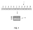
図1は、基板の上にパターン化された層を製作するための製作装置の実施形態を模式的及び例示的に示しており、前記基板は、層を形成する層材料が付与される第1領域と、層材料が付与されない第2領域とを有する。この実施形態では、基板14は、バリア層15及び導電層16で被覆されている。バリア層15は、好ましくは酸化シリコン層又は窒化シリコン層である。バリア層15は、10〜30nmの範囲の厚さを有する。導電層16は、この実施形態では、ITO層であり、150nmの厚さを有する。基板14、バリア層15、及び導電層16は層構造部13を形成し、これは製作装置1によって加工される。
FIG. 1 schematically and exemplarily shows an embodiment of a production device for producing a patterned layer on a substrate, the substrate being provided with a first layer material forming the layer. A region and a second region to which no layer material is applied. In this embodiment, the
前記製作装置1は、層構造部13を初期段階で洗浄するための初期洗浄ユニット2を含む。例えば、まず水のぬれ挙動が選択的に改善され、その後、複数のすすぎ工程及び/又は機械によるブラッシングが続く。通常、大きめのパーティクルを除去するこれらのステップの後、さらにその後で層構造部13がエアーナイフの下に移動され、次に赤外線加熱によって乾燥される前に、小さめのパーティクルを除去するために、超音波及びメガソニック洗浄ステップが続く。この工程の後、表面エネルギーを変更するために紫外線オゾン調整ステップが続く。
The manufacturing apparatus 1 includes an
前記製作装置1は、更に、基板の上、すなわち基板14の上のバリア層15とともに被覆された導電層16の上の第2領域に保護材料17を付与するための保護材料付与ユニット3を有する。この実施形態では、保護材料付与ユニット3は、印刷によって保護材料17を付与するのに適している。保護材料は、好ましくは、ホットワックスインクとも呼ばれるワックスインクである。使用されたワックスは、約90℃で液体になる。印刷後、温度が下がると、保護材料は固形化して保護膜を形成する。保護材料付与ユニット3は、好ましくは、例えばOce Technologies B.V.によって提供される熱インクジェット技術を使用するのに適している。図2は、結果として得られる保護材料17を備える層構造部を模式的及び例示的に示す。
The production apparatus 1 further comprises a protective
前記製作装置1は、更に、基板上の第1領域に液状層材料を印刷する、すなわちこの実施形態では、バリア層15及び導電層16を有する基板14の上の第1領域に液状層材料を印刷するための層材料付与ユニット4を有する。この実施形態では、層材料付与ユニット4は、インクジェット印刷又はスクリーン印刷を使用して、層材料として銀又は銅インクのような金属インクを使用するのに適している。金属インクは、プリントヘッドの中に金属インクが詰まるのを防ぐ量のポリマー及び金属ナノ粒子を含む。ポリマーは、金属残存成分及び個々のナノ粒子のみが一緒に融解する、以下に説明される焼結工程によって、後で除去される。例えば、25〜40体積パーセントのエタンジオール、25〜40体積パーセントのエタノール、10〜25体積パーセントのグリセリン、2.5〜5体積パーセントの2−イソプロポキシエタノール、及び3体積パーセントの銀から構成されるSunChemicals社の製品名”Suntronic U5603”という銀ナノ粒子性インクは、標準のDimatix Material Cartridges DMC11610を備えるDimatix DMP2800によって提供される金属インクのインクジェット技術と共に使用されうる。図3は、この実施形態において、層材料18に金属インクが印刷された後の層構造部を模式的及び例示的に示す。
The manufacturing apparatus 1 further prints the liquid layer material on the first region on the substrate, that is, in this embodiment, the liquid layer material is printed on the first region on the
層材料18が印刷された後、乾燥ユニット5が層材料18を、保護材料17の融解温度よりも低い乾燥温度まで加熱することによって乾燥させる。例えば、乾燥ユニット5は、層材料18を約80℃で、例えば15分間乾燥させるのに適している。乾燥ユニット5は、乾燥工程を行うための対流式オーブンを有しうる。
After the
前記製作装置1は、更に、パターン化された導電層16を生成するために、保護材料17を通して、及び/又は付与された層材料18を通して、導電層16を焼灼するための焼灼ユニット6を含む。この実施形態では、焼灼ユニット6は、保護材料及び/又は層材料を通して、レーザー焼灼を行うレーザーを有する。前記レーザーは、好ましくは、等しいパルスエネルギーを得るためのQ−スイッチモードを有する355nmで動作する半導体レーザーである。ビームプロファイルは、ガウス形状となりうるが、フラットトップ・プロファイル形状のような他の形状にもなりうる。結果として得られる層構造部は、図4に模式的及び例示的に示される。図4では、矢印20は焼灼ユニット6のレーザーを示す。
The fabrication apparatus 1 further includes an
前記レーザー焼灼は、好ましくは金属インクである層材料18及び/又は保護材料17の破片粒子を作り出しうる。それだけでなく、レーザー焼灼は、層材料16の破片を作り出しうる。図4では、破片粒子は参照番号19で示されている。レーザー焼灼は、偶発的に層材料に印刷されるのを回避するために、すなわち、この実施形態では、偶発的に金属が焼灼ライン上に印刷されるのを回避するために、層材料18が層構造部の上に印刷された後に行われる。層材料18を印刷した後の焼灼は、焼灼ラインが破片粒子によって覆われないであろうことを確実にし、保護材料17を印刷した後の焼灼は、焼灼からの破片が、保護材料17を除去した後の層16の上に残らないことを確実にする。
The laser ablation can produce debris particles of
前記製作装置1は、保護材料17の融解温度よりも高い除去温度を用いて、基板から保護材料17を除去するための保護材料除去ユニット7を更に含む。この実施形態では、保護材料除去ユニット7は、保護材料17を除去するのに加熱した水を使用するのに適している。特に、ワックスの融解温度よりも高い温度に加熱された水を用いて除去されるワックスが保護材料として好ましくは使用される。特に、前記水は、好ましくは約90℃又は95℃の温度まで加熱された蒸留水である。除去工程は、好ましくはスプレー‐ストリッピングで行われる。しかしながら、他の実施形態では、除去工程は他のストリッピング技術を使用して行われうる。例えば、保護材料除去ユニット7は、すすぎステーションのカスケードを有することができ、その中では、すすぎステーションからすすぎステーションへと進むほど、保護材料はより除去される。保護材料17の除去と共に、焼灼工程で作り出されたであろう破片粒子及び/又は金属インク、すなわち第2領域に誤って印刷された層材料も除去される。図5は、保護材料17が除去された後の層構造部を模式的又は例示的に示す。
The fabrication apparatus 1 further includes a protective
前記製作装置1は、層材料18を焼結するための焼結ユニット8を更に含む。焼結ユニット8は、好ましくは、130℃よりも高い温度で金属インクを焼結するのに適している。この焼結ステップは、保護材料17のあり得る薄い残存成分をも除去できるという副次的効果を有しうる。焼結は、従って、保護材料の残存成分が除去できるように行われうる。
The production apparatus 1 further includes a
前記製作装置1は、層材料の上に絶縁材料を付与するための絶縁材料付与ユニット9を更に含む。この実施形態では、絶縁材料21は、インクジェット印刷によって付与されるレジストである。前記レジストは、例えば、AZ1518のようなフォトレジストであり、当該フォトレジストには、好ましくは、上記の標準のDimatix Material Cartridges DMC11610を備えるDimatix DMP2800を用いるインクジェット技術が使用されうる。結果として得られる絶縁材料21を有する層構造部が模式的及び例示的に図6に示されている。
The manufacturing apparatus 1 further includes an insulating
前記製作装置1は、絶縁材料を硬化する、特に絶縁材料を加熱するための硬化ユニット10を更に含む。更に、前記製作装置1は、最終洗浄工程を行うための最終洗浄ユニット11を含む。当該最終洗浄ユニット11は、上記の初期洗浄と類似する最終洗浄を行うのに適している。前記初期洗浄と当該最終洗浄は、同一又は異なるユニットで行われうる。
The production device 1 further comprises a
前記製作装置1は、洗浄された層構造部を有する電気デバイスを製造するための電気デバイス製造ユニット12を更に含む。例えば、図7に模式的及び例示的に示されるように、電気デバイス製造ユニット12は、有機層27及び別の導電層28を層構造部の上に付与するのに適している。更に、電気デバイス製造ユニット12は、層構造部の上の防湿のためにゲッター23を金属ケーシング22に取り付けるのに適している。その後、別の導電層28と、有機層27に隣接する焼灼された導電パターン16の一部とが、既知の方法で光29を生成するのに有機材料27に電流を誘導するために、電気的接続部24、25を介して電源26に接続される。従って、別の導電層28は、好ましくは陰極であり、有機材料27に隣接する焼灼された導電層16の一部は、好ましくは陽極である。電気デバイス製造ユニット12によって製造された電気デバイスは、従って好ましくはOLEDである。
The manufacturing apparatus 1 further includes an electrical
以下に、基板の上にパターン化された層を製作するための製作方法の実施形態が、図8に示されるフローチャートを参照して例示的に説明されるだろう。 In the following, an embodiment of a fabrication method for fabricating a patterned layer on a substrate will be exemplarily described with reference to the flowchart shown in FIG.
ステップ101では、初期洗浄ユニット2は、バリア層15及び導電層16を有する基板14を洗浄する。ステップ102では、保護材料付与ユニット3は、層材料が付与されていない第2領域に保護材料を付与する。特に、保護材料付与ユニット5は、これら第2領域を保護するために、導電層16の上の第2領域にワックスを印刷する。ステップ103では、層材料付与ユニット4は、第1領域に層材料として金属インクを印刷し、当該第1領域には、金属が最終的に基板の上に、すなわち基板14の上のバリア層15を被覆する導電層16の上に存在しなければならない。ステップ104では、乾燥ユニット5が、保護材料の融解温度よりも低い乾燥温度まで金属インクを加熱することによって、金属インクを乾燥させ、ステップ105では、焼灼ユニット6は、保護材料17及びパターン化された導電層16を生成するために付与された金属18の少なくとも1つを通して導電層16を焼灼する。ステップ106では、保護材料除去ユニットは、加熱した水、例えば、保護材料、好ましくはワックスが液体になる温度である約90℃又は95℃の温度まで加熱された水によって、保護材料17を除去する。ステップ107では、焼結ユニット8は金属材料18を焼結し、ステップ108では、絶縁材料21が絶縁材料付与ユニット9を使用して付与される。付与された絶縁材料は、その後硬化され、具体的にはステップ109で、硬化ユニット10によって焼かれ、結果として得られる層構造部は、そのすぐ後で、ステップ110で最終洗浄ユニット11によって洗浄される。ステップ111では、電気デバイス製造ユニット12は、洗浄された層構造部を基礎とする電気デバイス、具体的にはOLEDを製造する。
In
OLED製作のための基板は、一般に広く、表面に透明導電性陽極被覆及び金属被覆が施されたディスプレイ用ガラスから作られている。陽極及び金属層は、両方とも電気的に絶縁された領域を実現するのにパターン化され、金属に関しては、光抽出のための窓を作り出すためである。一方、OLEDディスプレイや小さなデバイスでは、金属は通常、より大きなデバイスの中のデバイスのフレームを形成するのみであり、陽極材料の限られた導電性によって、均質な発光デバイスを実現するのに横方向電流分布を改善するために、付加的にサポートする精細金属構造が付与されうる。代替的な基板は、プラスチック材料のような他の材料でも作られうる。 Substrates for OLED fabrication are generally wide and are made of display glass with a transparent conductive anode coating and metal coating on the surface. Both the anode and the metal layer are patterned to provide an electrically isolated region, and for metal, to create a window for light extraction. On the other hand, in OLED displays and small devices, the metal usually only forms the device frame in larger devices, and the limited conductivity of the anode material allows the lateral direction to achieve a homogeneous light-emitting device. In order to improve the current distribution, an additional supporting fine metal structure can be provided. Alternative substrates can be made of other materials such as plastic materials.
現代の製作は、通常、主に陽極の全領域の被覆及び金属被覆だけでなくフォトリソグラフィーによって行われる後続のパターン化工程とを基礎にしている。多くの金属材料が無駄になるため、基板を、特に一連の小さな製品の基板を、高価な部品にする;フォトリソグラフィーは、マスクコスト及び必要な化学的性質のために環境保全性が限定されるため、高価である。 Modern fabrication is usually based mainly on the entire patterning of the anode and the metallization as well as the subsequent patterning process performed by photolithography. Many metal materials are wasted, making the substrate, especially a series of small product substrates, expensive components; photolithography has limited environmental integrity due to mask costs and required chemical properties Therefore, it is expensive.
フォトリソグラフィーの代わりに、本製作装置及び方法は、層材料を印刷するのに印刷工程、具体的には金属インクを使用する。一般に、層材料を不要領域に置くという合理的なリスクがある。当該リスクとは、スクリーン印刷によって、しばらく後に、メッシュの下にインクが入り込むことである;そうすると、その後で、インクは、上記陽極と接触し、層材料の制御されないアイランドを形成する。インクジェット印刷を見ると、層材料のこの人工的及び不要な堆積は、ノズル閉塞、スプレー、サテライト、点火シーケンス及び他のパラメータに帰しうる。他の印刷技術には、他の理由が当てはまる。印刷パラメータは、その効果をある程度にまで抑制するように最適化できるが、長期的には、多少人工的な堆積が起こるであろう。 Instead of photolithography, the fabrication apparatus and method uses a printing process, specifically a metallic ink, to print the layer material. In general, there is a reasonable risk of placing layer material in unwanted areas. The risk is that after a while, by screen printing, the ink enters under the mesh; after that, the ink contacts the anode and forms an uncontrolled island of layer material. When looking at ink jet printing, this artificial and unwanted deposition of layer material can be attributed to nozzle blockage, spraying, satellites, ignition sequences and other parameters. Other reasons apply to other printing technologies. The printing parameters can be optimized to suppress the effect to some extent, but in the long term, some artificial deposition will occur.
サイズに大きな違いのある電気デバイスのそれらアイランドの結果として、具体的には、それらの上に設けられるOLEDは、非常に信頼性が低くなる。OLEDの場合は、これは一方で、一般に、粒子は薄いOLEDにとって危険であるため、有機材料の堆積中のシェーディング効果が原因で、それによって、有機材料のより薄い層又は金属が結果として生じ、あるいは、陰極との直接的な短絡を形成さえする。他方で、寿命期間内のサテライト堆積から発して陰極への材料の移動が、信頼性を限られたものにする。一度それが起こると、それらのスポットの周辺で劇的に増加する電界強度が電流の増加をもたらし、それ自体が高温、及び、次に電流の更なる増加を引き起こす有機材料の減少された耐性という結果につながる。総合的な効果は、この位置での有機材料の劇的に減少された寿命期間及び/又はデバイスを破壊することになる電気的短絡の形成である。 As a result of those islands of electrical devices with large differences in size, specifically, OLEDs provided on them are very unreliable. In the case of OLEDs this is, on the other hand, generally because particles are dangerous for thin OLEDs, due to shading effects during the deposition of organic material, thereby resulting in a thinner layer or metal of organic material, Alternatively, it can even form a direct short circuit with the cathode. On the other hand, the transfer of material from the satellite deposition during the lifetime to the cathode makes the reliability limited. Once that happens, the dramatically increasing electric field strength around those spots leads to an increase in current, which in itself is a reduced resistance of organic materials that causes a further increase in current and then the current. Leads to results. The overall effect is the dramatically reduced lifetime of the organic material at this location and / or the formation of an electrical short that will destroy the device.
本製作装置及び方法は、層材料を印刷する前に保護膜を施すことによって、層材料の存在が意図された領域又は層材料が誤って被着された場合であっても危険ではない領域にのみ層材料、具体的には金属を被着することを確実なものとするための手法を用いる。この膜は、アクティブ領域を覆うことができるので、誤ってこの領域に印刷された層材料は、この膜の上に存在する。金属が焼結する前に、膜は潜在的に存在する不要な金属と共に除去され、例えばOLED堆積に対してクリーンな表面を残す。 This fabrication apparatus and method can be applied to areas where the layer material is intended to be present or areas that are not dangerous even if the layer material is accidentally deposited by applying a protective film before printing the layer material. Only techniques are used to ensure deposition of layer material, specifically metal. Since this film can cover the active area, layer material that is accidentally printed in this area will be present on this film. Before the metal sinters, the film is removed along with potentially unwanted unwanted metal, leaving a clean surface, for example, for OLED deposition.
保護膜、すなわち保護材料は、好ましくは、同様に印刷された層材料を除去することなく完全に除去されるのに適している。保護膜の上の不要な層材料だけが、保護膜の除去と共に除去されるべきである。これら2つの要求の組み合わせ、すなわち、i)保護膜を完全に除去する、及びii)印刷された層材料を除去しない、を満足させるのは複雑である、なぜならば、一方で、印刷された層材料は乾燥させるため及び保護のための除去工程に耐性を持たせるために加熱され、他方で、熱処理は保護材料にも同じ効果を与えるからである。従って、加熱によって、除去が不可能になるであろうという傾向が増す。それは一方で、基板への接着力を増すために層材料を加熱することは、保護材料の接着力を増すことでもあり、よって、保護材料及び層材料の両方を除去する、すなわち乾燥させない、あるいは、いずれをも除去しない、すなわち乾燥させる、のいずれかである。本製作装置及び方法は、両方の要求を解決する解決策を、上記特性を有する保護材料を使用することによって、具体的には保護材料としてワックスを使用し、及び前述の製作ステップを付与することによって、提供する。 The protective film, i.e. the protective material, is preferably suitable for being completely removed without removing the printed layer material as well. Only the unwanted layer material on the protective film should be removed with the removal of the protective film. It is complicated to satisfy the combination of these two requirements: i) complete removal of the overcoat and ii) no removal of the printed layer material, because on the other hand the printed layer This is because the material is heated to dry and to withstand the removal process for protection, while the heat treatment has the same effect on the protection material. Therefore, there is an increased tendency that heating will make removal impossible. On the other hand, heating the layer material to increase the adhesion to the substrate also increases the adhesion of the protective material, thus removing both the protective material and the layer material, i.e. not drying, or None of them are removed, i.e. dried. The fabrication apparatus and method provides a solution that solves both requirements by using a protective material having the above properties, specifically using wax as the protective material, and providing the aforementioned fabrication steps. By, provide.
上記の実施形態の中で、前記製作装置はOLEDを製作するのに適用されているが、前記製作装置は、基板の上にパターン化された層、具体的には基板の上にパターン化された第1層及びパターン化された第2層を有する層構造部をただ製作するだけのために適用することもできる。特に、製作装置は、図6に示された層構造部をただ製作するだけのために適用することもできる。製作された層構造部は、その後、OLED又は他の電気デバイスを製造するための基礎として使用されうる。 In the above embodiment, the fabrication apparatus is applied to fabricate an OLED, but the fabrication apparatus is patterned on a substrate, specifically, patterned on the substrate. It can also be applied to merely produce a layer structure with a first layer and a patterned second layer. In particular, the production apparatus can be applied only for producing the layer structure shown in FIG. The fabricated layer structure can then be used as a basis for manufacturing OLEDs or other electrical devices.
図、開示、及び添付の請求項の解釈から、請求項に記載された発明を実行する際に、開示された実施形態に対する他のバリエーションは、当業者によって理解され、実効されうる。 From the illustrations, disclosure, and interpretation of the appended claims, other variations to the disclosed embodiments can be understood and effected by those skilled in the art in practicing the claimed invention.
請求項で、単語「有する”comprising”」は、他の要素やステップを除外するものではなく、不定冠詞“a”又は“an”は、複数を除外するものではない。 In the claims, the word “comprising” does not exclude other elements or steps, and the indefinite article “a” or “an” does not exclude a plurality.
単一ユニット又はデバイスは、請求項の中で述べられた複数項目の機能を満たすことができる。特定の手段が、相互に異なる従属請求項の中で述べられているという単なる事実は、これらの手段の組み合わせを効果的に使用することができないと説明しているわけではない。 A single unit or device may fulfill the functions of several items recited in the claims. The mere fact that certain measures are recited in mutually different dependent claims does not indicate that a combination of these measures cannot be used effectively.
1又は複数のユニット又はデバイスによって行われる保護材料及び層材料の付与、焼灼、保護材料の剥離等のような処理ステップは、任意の他のユニット又はデバイスによって行うことができる。 Processing steps such as application of protective and layer materials, cauterization, stripping of protective material, etc. performed by one or more units or devices can be performed by any other unit or device.
コンピュータプログラムは、光学記憶媒体又は半導体媒体といった適当な媒体に記憶/分散され、他のハードウェアと共に、又は他のハードウェアの一部として供給されるが、インターネット又は他の有線又は無線電気通信システムといった他の形式で分配することもできる。 The computer program may be stored / distributed on a suitable medium, such as an optical storage medium or a semiconductor medium, and supplied with other hardware or as part of other hardware, but the Internet or other wired or wireless telecommunication systems Can be distributed in other formats.
請求項中の参照記号は、請求の範囲を限定すると解釈されるべきではない。 Reference signs in the claims shall not be construed as limiting the scope.
本発明は、基板の上にパターン化された層を製作するための製作装置に関する。保護材料が前記基板の上の第2領域に付与され、液状層材料が、その後、前記基板の上の前記第2領域とは異なる第1領域に印刷される。前記層材料は、前記保護材料の融解温度よりも高い除去温度を用いて、前記基板から前記保護材料を除去する前に、前記保護材料の融解温度よりも低い乾燥温度まで、前記層材料を加熱することによって乾燥される。パターン化された層が、従って、例えば費用のかかるフォトリソグラフィー工程を使用せずに製造でき、前記保護材料を使用することで、前記層材料は所望の前記第1領域にのみ存在し、前記第2領域には存在しない。これは、OLEDを製造するために使用される前記パターン化された層の品質を向上させる。
The present invention relates to a fabrication apparatus for fabricating a patterned layer on a substrate. A protective material is applied to the second region on the substrate, and the liquid layer material is then printed on a first region different from the second region on the substrate. The layer material heats the layer material to a drying temperature lower than the melting temperature of the protective material before removing the protective material from the substrate using a removal temperature higher than the melting temperature of the protective material. To be dried. A patterned layer can thus be produced, for example, without using an expensive photolithography process, and by using the protective material, the layer material is present only in the desired first region, and the first layer There are no two areas. This improves the quality of the patterned layer used to manufacture the OLED.
Claims (10)
前記基板の上の前記第2領域に保護材料を付与する保護材料付与ユニットと、
前記基板の上の前記第1領域に液状層材料を印刷する層材料付与ユニットと、
前記保護材料の融解温度よりも低い乾燥温度まで、前記層材料を加熱することによって、前記層材料を乾燥させる乾燥ユニットと、
前記パターン化された導電層を生成するために、付与された前記層材料と前記保護材料とのうちの少なくとも1つを通して前記導電層を焼灼する焼灼ユニットと、
前記保護材料の前記融解温度よりも高い除去温度を用いて、前記基板から前記保護材料を除去する保護材料除去ユニットと、
を有する、製作装置。 In a fabrication apparatus for fabricating a patterned layer on a substrate coated with a patterned conductive layer, the substrate has a first region to which a layer material for forming the patterned layer is applied. And a second region to which the layer material is not applied, and the manufacturing apparatus includes:
A protective material applying unit for applying a protective material to the second region on the substrate;
A layer material application unit for printing a liquid layer material on the first region on the substrate;
A drying unit for drying the layer material by heating the layer material to a drying temperature lower than the melting temperature of the protective material;
An ablation unit that cauterizes the conductive layer through at least one of the applied layer material and the protective material to produce the patterned conductive layer;
A protective material removal unit that removes the protective material from the substrate using a removal temperature higher than the melting temperature of the protective material;
A production apparatus having
前記基板の上の前記第2領域に保護材料を付与するステップと、
前記基板の上の前記第1領域に液状層材料を印刷するステップと、
前記保護材料の融解温度よりも低い乾燥温度まで、前記層材料を加熱することによって、前記層材料を乾燥させるステップと、
前記パターン化された導電層を生成するために、付与された前記層材料と前記保護材料とのうちの少なくとも1つを通して前記導電層を焼灼するステップと、
前記保護材料の前記融解温度よりも高い除去温度を用いて、前記基板から前記保護材料を除去するステップと、
を有する、製作方法。 In a fabrication method for fabricating a patterned layer on a substrate coated with a patterned conductive layer, a first region to which the substrate is applied a layer material that forms the layer; and the layer material A second region to which is not provided, and the manufacturing method includes:
Applying a protective material to the second region on the substrate;
Printing a liquid layer material on the first region on the substrate;
Drying the layer material by heating the layer material to a drying temperature lower than the melting temperature of the protective material;
Cauterizing the conductive layer through at least one of the applied layer material and the protective material to produce the patterned conductive layer;
Removing the protective material from the substrate using a removal temperature higher than the melting temperature of the protective material;
A manufacturing method.
Applications Claiming Priority (3)
| Application Number | Priority Date | Filing Date | Title |
|---|---|---|---|
| EP11167070 | 2011-05-23 | ||
| EP11167070.9 | 2011-05-23 | ||
| PCT/IB2012/052292 WO2012160468A1 (en) | 2011-05-23 | 2012-05-09 | Fabrication apparatus for fabricating a patterned layer |
Publications (3)
| Publication Number | Publication Date |
|---|---|
| JP2014517998A JP2014517998A (en) | 2014-07-24 |
| JP2014517998A5 JP2014517998A5 (en) | 2015-06-25 |
| JP6058640B2 true JP6058640B2 (en) | 2017-01-11 |
Family
ID=46208109
Family Applications (1)
| Application Number | Title | Priority Date | Filing Date |
|---|---|---|---|
| JP2014511980A Expired - Fee Related JP6058640B2 (en) | 2011-05-23 | 2012-05-09 | Production equipment for producing patterned layers |
Country Status (5)
| Country | Link |
|---|---|
| US (1) | US9472787B2 (en) |
| EP (1) | EP2715829B1 (en) |
| JP (1) | JP6058640B2 (en) |
| CN (1) | CN103548174B (en) |
| WO (1) | WO2012160468A1 (en) |
Families Citing this family (3)
| Publication number | Priority date | Publication date | Assignee | Title |
|---|---|---|---|---|
| EP2715830B1 (en) * | 2011-05-23 | 2019-08-28 | OLEDWorks GmbH | Method for fabricating a layer structure |
| JP6434029B2 (en) | 2013-09-06 | 2018-12-05 | ソルベイ スペシャルティ ポリマーズ イタリー エス.ピー.エー. | Conductive assembly |
| JP6836908B2 (en) * | 2017-01-10 | 2021-03-03 | 住友化学株式会社 | Manufacturing method of organic device |
Family Cites Families (13)
| Publication number | Priority date | Publication date | Assignee | Title |
|---|---|---|---|---|
| US20030148024A1 (en) | 2001-10-05 | 2003-08-07 | Kodas Toivo T. | Low viscosity precursor compositons and methods for the depositon of conductive electronic features |
| AU2002347164A1 (en) * | 2001-12-21 | 2003-07-15 | Ifire Technology Inc. | Method of laser ablation for patterning thin film layers for electroluminescent displays |
| KR100778286B1 (en) * | 2001-12-29 | 2007-11-22 | 엘지.필립스 엘시디 주식회사 | manufacturing method of organic electroluminescence displays |
| US7288469B2 (en) | 2004-12-03 | 2007-10-30 | Eastman Kodak Company | Methods and apparatuses for forming an article |
| TW200640596A (en) | 2005-01-14 | 2006-12-01 | Cabot Corp | Production of metal nanoparticles |
| US7510951B2 (en) * | 2005-05-12 | 2009-03-31 | Lg Chem, Ltd. | Method for forming high-resolution pattern with direct writing means |
| KR100833017B1 (en) * | 2005-05-12 | 2008-05-27 | 주식회사 엘지화학 | Method for preparing a high resolution pattern with direct writing means |
| ATE493766T1 (en) * | 2005-06-30 | 2011-01-15 | Koninkl Philips Electronics Nv | METHOD FOR GENERATING AN ELECTRODE LAYER PATTERN IN AN ORGANIC FUNCTIONAL DEVICE |
| KR100690930B1 (en) * | 2006-05-03 | 2007-03-09 | 한국기계연구원 | Method for preparing a high resolution pattern with a high aspect ratio and the pattern thickness required by using deep ablation |
| JP4356899B2 (en) * | 2007-03-15 | 2009-11-04 | 財団法人山形県産業技術振興機構 | Organic EL light emitting device and method for manufacturing the same |
| DE102007043182A1 (en) * | 2007-09-11 | 2009-03-12 | Osram Opto Semiconductors Gmbh | Thick strip conductor producing method for e.g. LED, involves providing openings such that upper side of carrier is exposed in openings, and introducing conductor material containing electrically conductive particles in openings |
| EP2086033A1 (en) * | 2008-01-31 | 2009-08-05 | Applied Materials, Inc. | Method of coating a substrate and coating installation |
| US8659220B2 (en) * | 2010-06-07 | 2014-02-25 | Nec Lighting, Ltd. | Organic electroluminescent lighting device |
-
2012
- 2012-05-09 CN CN201280024866.5A patent/CN103548174B/en not_active Expired - Fee Related
- 2012-05-09 JP JP2014511980A patent/JP6058640B2/en not_active Expired - Fee Related
- 2012-05-09 EP EP12725503.2A patent/EP2715829B1/en not_active Not-in-force
- 2012-05-09 US US14/117,436 patent/US9472787B2/en not_active Expired - Fee Related
- 2012-05-09 WO PCT/IB2012/052292 patent/WO2012160468A1/en active Application Filing
Also Published As
| Publication number | Publication date |
|---|---|
| EP2715829B1 (en) | 2016-06-29 |
| US9472787B2 (en) | 2016-10-18 |
| US20140203250A1 (en) | 2014-07-24 |
| CN103548174A (en) | 2014-01-29 |
| CN103548174B (en) | 2016-09-28 |
| EP2715829A1 (en) | 2014-04-09 |
| JP2014517998A (en) | 2014-07-24 |
| WO2012160468A1 (en) | 2012-11-29 |
Similar Documents
| Publication | Publication Date | Title |
|---|---|---|
| JP5355059B2 (en) | Method for forming multilayer electrode structure on solar cell, metal wiring contact structure, layer patterning method, functional structure forming method | |
| KR100955540B1 (en) | heat generation sheet and fabrication method thereof | |
| JP6688225B2 (en) | Method for manufacturing graphene layer | |
| US9050775B2 (en) | Methods of fabricating transparent and nanomaterial-based conductive film | |
| JP6058640B2 (en) | Production equipment for producing patterned layers | |
| JP5850908B2 (en) | Method for manufacturing an OLED having a spatially isolated light emitting region | |
| JP6009548B2 (en) | Manufacturing equipment for manufacturing layered structures | |
| TW201145565A (en) | Method of maskless manufacturing of OLED devices | |
| EP2333859B1 (en) | A method for forming an organic light emitting diode | |
| EP2720086A1 (en) | Methods of fabricating transparent and nanomaterial-based conductive film | |
| KR101069582B1 (en) | A cathode electrode having carbon nanotube in an electrical field emission device and a fabrication method thereof | |
| Shin et al. | Photoresist-free lithographic patterning of solution-processed nanostructured metal thin films | |
| KR20100032237A (en) | Heat generation sheet and fabrication method thereof | |
| TW201126786A (en) | Architecture for organic electronic devices | |
| US7923837B2 (en) | Microelectronic device patterned by ablating and subsequently sintering said microelectronic device | |
| JP2005086188A (en) | Formation method for film pattern and formation equipment, and circuit element | |
| JP2011023445A (en) | Method of manufacturing multilayer wiring board, and multilayer wiring board | |
| Liu et al. | Metal cathode patterning for OLED by nanosecond pulsed laser ablation |
Legal Events
| Date | Code | Title | Description |
|---|---|---|---|
| A521 | Request for written amendment filed |
Free format text: JAPANESE INTERMEDIATE CODE: A523 Effective date: 20150507 |
|
| A621 | Written request for application examination |
Free format text: JAPANESE INTERMEDIATE CODE: A621 Effective date: 20150507 |
|
| A977 | Report on retrieval |
Free format text: JAPANESE INTERMEDIATE CODE: A971007 Effective date: 20160303 |
|
| A131 | Notification of reasons for refusal |
Free format text: JAPANESE INTERMEDIATE CODE: A131 Effective date: 20160411 |
|
| A711 | Notification of change in applicant |
Free format text: JAPANESE INTERMEDIATE CODE: A711 Effective date: 20160426 |
|
| A521 | Request for written amendment filed |
Free format text: JAPANESE INTERMEDIATE CODE: A523 Effective date: 20160711 |
|
| TRDD | Decision of grant or rejection written | ||
| A01 | Written decision to grant a patent or to grant a registration (utility model) |
Free format text: JAPANESE INTERMEDIATE CODE: A01 Effective date: 20161109 |
|
| A61 | First payment of annual fees (during grant procedure) |
Free format text: JAPANESE INTERMEDIATE CODE: A61 Effective date: 20161207 |
|
| R150 | Certificate of patent or registration of utility model |
Ref document number: 6058640 Country of ref document: JP Free format text: JAPANESE INTERMEDIATE CODE: R150 |
|
| LAPS | Cancellation because of no payment of annual fees |