JP6053262B2 - Optical element, optical system and optical apparatus using the same - Google Patents
Optical element, optical system and optical apparatus using the same Download PDFInfo
- Publication number
- JP6053262B2 JP6053262B2 JP2011169008A JP2011169008A JP6053262B2 JP 6053262 B2 JP6053262 B2 JP 6053262B2 JP 2011169008 A JP2011169008 A JP 2011169008A JP 2011169008 A JP2011169008 A JP 2011169008A JP 6053262 B2 JP6053262 B2 JP 6053262B2
- Authority
- JP
- Japan
- Prior art keywords
- layer
- optical element
- refractive index
- binder
- fine particles
- Prior art date
- Legal status (The legal status is an assumption and is not a legal conclusion. Google has not performed a legal analysis and makes no representation as to the accuracy of the status listed.)
- Active
Links
Images


Classifications
-
- G—PHYSICS
- G02—OPTICS
- G02B—OPTICAL ELEMENTS, SYSTEMS OR APPARATUS
- G02B1/00—Optical elements characterised by the material of which they are made; Optical coatings for optical elements
- G02B1/10—Optical coatings produced by application to, or surface treatment of, optical elements
- G02B1/11—Anti-reflection coatings
- G02B1/118—Anti-reflection coatings having sub-optical wavelength surface structures designed to provide an enhanced transmittance, e.g. moth-eye structures
-
- G—PHYSICS
- G02—OPTICS
- G02B—OPTICAL ELEMENTS, SYSTEMS OR APPARATUS
- G02B1/00—Optical elements characterised by the material of which they are made; Optical coatings for optical elements
- G02B1/10—Optical coatings produced by application to, or surface treatment of, optical elements
- G02B1/14—Protective coatings, e.g. hard coatings
-
- Y—GENERAL TAGGING OF NEW TECHNOLOGICAL DEVELOPMENTS; GENERAL TAGGING OF CROSS-SECTIONAL TECHNOLOGIES SPANNING OVER SEVERAL SECTIONS OF THE IPC; TECHNICAL SUBJECTS COVERED BY FORMER USPC CROSS-REFERENCE ART COLLECTIONS [XRACs] AND DIGESTS
- Y10—TECHNICAL SUBJECTS COVERED BY FORMER USPC
- Y10T—TECHNICAL SUBJECTS COVERED BY FORMER US CLASSIFICATION
- Y10T428/00—Stock material or miscellaneous articles
- Y10T428/24—Structurally defined web or sheet [e.g., overall dimension, etc.]
- Y10T428/24942—Structurally defined web or sheet [e.g., overall dimension, etc.] including components having same physical characteristic in differing degree
- Y10T428/2495—Thickness [relative or absolute]
- Y10T428/24967—Absolute thicknesses specified
- Y10T428/24975—No layer or component greater than 5 mils thick
Description
本発明は、光学素子、それを用いた光学系および光学機器に関する。 The present invention relates to an optical element, an optical system using the optical element, and an optical apparatus.
従来、ビデオカメラ、写真カメラ、またはテレビカメラなどの光学機器に用いられる撮影レンズでは、その結像光学系に採用される光学素子の両面または片面に、透過光量を上げ、不要光によるゴーストやフレアを回避するための反射防止膜が施されている。特に、近年のビデオカメラやテレビカメラにおけるHDなどの高精細化、および写真カメラにおける高画質化に伴い、反射防止性能も高性能化が求められている。ここで、高性能な反射防止性能を得るためには、反射防止膜の最表層に用いられる材料を、屈折率の低い材料とする必要がある。この屈折率の低い材料としては、例えば、シリカやフッ化マグネシウムなどの無機系材料、またはシリコーン樹脂や非晶質のフッ素樹脂などの有機材料などがある。さらに、シリカやフッ化マグネシウムの層内に空隙を形成することで、より屈折率を低く抑える技術も存在する。例えば、屈折率が1.38のフッ化マグネシウムの薄膜層内に30%(体積)の空隙を設けると、屈折率を1.27まで下げることができる。このような層内に空隙を形成する方法として、特許文献1は、シリカやフッ化マグネシウム微粒子をバインダーと共に成膜し、微粒子間に空隙が形成された低屈折率材料を用いる反射防止膜(シリカエアロゲル膜)の製造方法を開示している。これに対して、特許文献2は、内部が空洞である中空微粒子をバインダーで結合させて形成し、さらに中空微粒子間に別のバインダーを充填して微粒子間の結合を強化した低屈折率層を有する反射防止膜とその製造方法を開示している。
Conventionally, in a photographic lens used in an optical apparatus such as a video camera, a photographic camera, or a television camera, a ghost or flare caused by unnecessary light is increased by increasing the amount of transmitted light on both sides or one side of an optical element used in the imaging optical system. An antireflection film for avoiding the above is applied. In particular, with high definition such as HD in video cameras and television cameras in recent years and high image quality in photo cameras, high performance in antireflection performance is also required. Here, in order to obtain high-performance antireflection performance, the material used for the outermost layer of the antireflection film needs to be a material having a low refractive index. Examples of the material having a low refractive index include inorganic materials such as silica and magnesium fluoride, and organic materials such as silicone resin and amorphous fluorine resin. Furthermore, there is a technique for further reducing the refractive index by forming voids in the silica or magnesium fluoride layer. For example, if a 30% (volume) void is provided in a magnesium fluoride thin film layer having a refractive index of 1.38, the refractive index can be lowered to 1.27. As a method for forming voids in such a layer,
ここで、特許文献2に示す反射防止膜では、中空微粒子が低屈折率層内に高充填され、かつ、バインダーが中空微粒子間の空隙に充填されることで中空微粒子間の結合を強化して、中空微粒子の内部の空洞により低屈折率を確保する。しかしながら、バインダーの高充填は、結果的に屈折率が高くなる一因となり得る。
Here, in the antireflection film shown in
本発明は、このような状況を鑑みてなされたものであり、低屈折率を確保しつつ、耐擦傷性に優れ、さらに高い反射防止性能を有する光学素子を提供することを目的とする。 The present invention has been made in view of such circumstances, and an object of the present invention is to provide an optical element having excellent scratch resistance and higher antireflection performance while ensuring a low refractive index.
上記課題を解決するために、本発明は、基材と、該基材上に形成された反射防止膜と、を有する光学素子であって、反射防止膜は、複数の中空微粒子と、該中空微粒子を互いに結合するバインダーと、を有する低屈折率層を含み、低屈折率層は、最表層としての第1層と、該第1層に隣接して基材の側に位置する第2層と、からなり、第1層でのバインダーの充填率は、第2層でのバインダーの充填率よりも低く、第1層での中空微粒子の充填率は、第2層での中空微粒子の充填率よりも低く、第1層のd線に対する屈折率は、1.1以上1.25以下であり、第1層は、バインダーの充填率が互いに異なる上層及び下層を含み、下層でのバインダーの充填率は、第2層でのバインダーの充填率よりも高いことを特徴とする。 In order to solve the above problems, the present invention provides an optical element having a base material and an antireflection film formed on the base material, the antireflection film comprising a plurality of hollow fine particles and the hollow A low-refractive-index layer having a binder that binds fine particles to each other, the low-refractive-index layer being a first layer as an outermost layer, and a second layer located adjacent to the first layer on the side of the substrate The filling rate of the binder in the first layer is lower than the filling rate of the binder in the second layer, and the filling rate of the hollow fine particles in the first layer is the filling rate of the hollow fine particles in the second layer. The refractive index for the d-line of the first layer is 1.1 or more and 1.25 or less, and the first layer includes an upper layer and a lower layer having different binder filling rates, and the binder of the lower layer The filling rate is characterized by being higher than the filling rate of the binder in the second layer.
本発明によれば、低屈折率を確保しつつ、耐擦傷性に優れ、さらに高い反射防止性能を有する光学素子を提供することができる。 According to the present invention, it is possible to provide an optical element having excellent anti-scratch performance and high antireflection performance while ensuring a low refractive index.
以下、本発明を実施するための形態について図面等を参照して説明する。 Hereinafter, embodiments for carrying out the present invention will be described with reference to the drawings.
(第1実施形態)
まず、本発明の第1実施形態に係る光学素子について説明する。図1は、本実施形態に係る光学素子1の構成を示す概略断面図である。この光学素子1は、光透過性を有する基材2と、この基材2の表面上(基材上)に形成された反射防止膜である低屈折率層3とを含む。ここで、「反射防止膜」とは、例えば、ビデオカメラなどの光学機器に用いられる撮影レンズにて、その結像光学系に採用される光学素子の両面または片面に形成され、透過光量を上げて、不要光によるゴーストやフレアを回避するための膜を示す。まず、基材2は、例えば、石英などのガラスや、樹脂などからなる透明部材である。また、基材2の形状は、図1では説明の簡単化のために平板(平面)としているが、例えば曲板やフィルム状板でもよく、また、低屈折率層3が形成される表面も、曲面、凹面、または凸面であってもよい。
(First embodiment)
First, the optical element according to the first embodiment of the present invention will be described. FIG. 1 is a schematic cross-sectional view showing the configuration of the
低屈折率層3は、多数の中空微粒子4をバインダー5で相互に結合させた膜からなる。また、中空微粒子4は、内部に空孔6を有するシェル7からなる。この中空微粒子4は、空孔6に含まれる空気(屈折率1.0)により屈折率を下げる性質を有する。なお、空孔6は、単孔または多孔のどちらでもよく、適宜選択される。さらに、シェル7を構成する材料(材質)としては、屈折率の低いものが好ましく、例えば、SiO2(シリカ)、MgF2、フッ素、またはシリコーンなどの有機樹脂が上げられるが、粒子の製造が容易であるSiO2がより好ましい。また、低屈折率層3は、最表層として配置され、中空微粒子4に対するバインダー5の充填率が低い第1層3aと,最表層の下部で基材2の側に位置する下層部として配置され、バインダー5の充填率が高い第2層3bとの2つの隣接した層を含む。このバインダー5の充填率は、バインダー5の希釈濃度を変更することで調整できる。まず、第1層3aでは、中空微粒子4は、図1に示すように不均一に配置されており、バインダー5の充填率が低いため、各中空微粒子4の間の空隙(空気)8の量が多くなることで、屈折率がより低くなる。ここで、中空微粒子4の粒径(ばらつきがある場合は平均粒径)は、20nm以上70nm以下、より好ましくは30nm以上60nm以下とすることが望ましい。これは、中空微粒子4の粒径が20nm未満の場合には、空孔6の大きさが小さくなり、屈折率を低くすることが難しく、粒径が60nm以上になると、粒子間の空隙の大きさが大きくなり、粒子の大きさに伴う散乱が発生し好ましくないためである。また、第1層3aの膜厚は、20nm以上70nm以下とし、一方、第1層3aの屈折率は、1.1以上1.25以下とすることが望ましい。次に、第2層3bでは、各中空微粒子4は、その間の空隙にバインダー5が充填されることで結合されているため、第2層3bは、強度が増加し、結果的に膜の耐擦傷性が保たれている。ここで、第2層3bの屈折率は、1.26以上1.35以下とすることが望ましい。最終的に、低屈折率層3の膜厚は、反射防止性能を得るために、90nm以上150nm以下とすることが望ましい。
The low
この低屈折率層3の形成に際しては、まず、例えば、ディップコート法、スピンコート法、スプレーコート法、またはロールコート法などの塗工方法(湿式成膜法)を用いて、基材2の表面上に中空微粒子4とバインダー5との混合液を塗工(塗布)する。特に、本実施形態の塗工処理では、レンズ表面のような曲面を有する基材に対しても膜厚を均一として成膜可能な観点から、スピンコート法の採用が好適である。次に、基材2上の塗工された混合液を乾燥させる。この乾燥処理は、ホットプレートや電気炉などを用いて実施される。このときの乾燥条件としては、基材2に影響を与えず、かつ、中空微粒子4内の有機溶媒を蒸発させることが可能な程度の温度と時間とに設定し、この温度は、例えば300℃以下とすることが望ましい。なお、通常、1回の塗工処理で低屈折率層3の膜を形成することが望ましいが、塗工処理と乾燥処理とを複数回繰り返して形成してもよい。
In forming the low
次に、本実施形態の光学素子1の具体例として、材質および数値を示し、その効果について説明する。まず、基材2は、d線(587.6nm)での屈折率が1.52である透明ガラス基板とする。次に、低屈折率層3における第2層3bの屈折率が1.30になるように、中空SiO2含有溶液に対するバインダー溶液の重量比率を1:0.71として混合液を生成する。このとき、低屈折率層3における第1層3aでのバインダー5の充填率が、第2層3bでのバインダー5の充填率よりも低くなるように、バインダー溶液の濃度を調整する。次に、上記混合液を基材2の表面上に滴下し、スピンコーター(3000rpm、30秒間回転)により塗工処理する。次に、この塗工処理が終了したものを、クリーンオーブン(200℃、1時間焼成)により乾燥処理する。これにより、基材2上に低屈折率層3を有する光学素子1が形成される。
Next, as a specific example of the
次に、反射率測定器により、光学素子1における波長400nmから700nmの反射率を測定した。図2は、この反射率測定の結果である反射率特性を示すグラフであり、横軸は、波長(nm)であり、縦軸は、反射率(%)である。この図2において、実線は、入射角0度の反射率特性を示し、一方、点線は、入射角45度の反射率特性を示す。図2に示すように、本実施形態の光学素子1によれば、波長400nmから700nmまでの全域0度反射で0.7%以下、一方、45度反射でも2.0%以下の良好な反射防止性能が確認できる。また、低屈折率層3の断面の状態を走査型透過電子顕微鏡により観察すると、低屈折率層3において、中空微粒子4の充填密度(バインダー5の充填率)の異なる第1層3aと第2層3bとを確認できる。本例の場合、この断面観察と反射率測定との結果より、低屈折率層3の膜厚は、125nmであることが確認できる。同様に、第1層3aの屈折率は、1.15であり、第1層3aの膜厚(物理膜厚)は、45nmであり、第2層3bの屈折率は、1.30であり、第2層3bの膜厚(物理膜厚)は、80nmであることもそれぞれ確認できる。なお、(表1)は、この光学素子1の構成に対する屈折率および膜厚を、基材2側から順に示す表である。
Next, the reflectance at a wavelength of 400 nm to 700 nm in the

さらに、光学素子1に対して、コットン布クリント(旭化成ケミカルズ株式会社の商品名)で300g/cm2の荷重を負荷し、20回往復させた後、低屈折率層3の表面を確認しても、傷が観察されない。
Further, a load of 300 g / cm 2 was applied to the
以上のように、本実施形態によれば、低屈折率を確保しつつ、耐擦傷性に優れ、さらに高い反射防止性能を有する光学素子を提供することができる。 As described above, according to the present embodiment, it is possible to provide an optical element having excellent scratch resistance and higher antireflection performance while ensuring a low refractive index.
(第2実施形態)
次に、本発明の第2実施形態に係る光学素子について説明する。第1実施形態の光学素子1は、基材2上に低屈折率層3のみを有するが、例えば、基材2と低屈折率層3との間に、高屈折率層や中屈折率層などを単層または複数層として有する構成もあり得る。この高屈折率層または中屈折率層としては、例えば、酸化ジルコニウム酸化チタン、酸化タンタル、酸化ニオブ、酸化ハフニウム、アルミナ、シリカ、またはフッ化マグネシウムなどの少なくともいずれかの材料を含む層が適用される。さらに、低屈折率層3における外部環境と接する表面に、撥水や撥油などの機能性を有する層を形成してもよい。この機能層の材料としては、例えば、フッ素を含有した塗料や、シリコーン塗料などが採用可能である。なお、このような屈折率層や機能層は、真空蒸着法、スパッタ法、CVD法、ディップコート法、スピンコート法、スプレーコート法などを用いて形成できる。
(Second Embodiment)
Next, an optical element according to a second embodiment of the present invention will be described. The
次に、本実施形態の光学素子の具体例として、材質および数値を示し、その効果について説明する。図3は、本実施形態に係る光学素子10の構成を示す概略断面図である。まず、基材11は、d線(587.6nm)での屈折率が1.806である透明ガラス基板とする。次に、この基材11上に、本実施形態の特徴である多層反射防止膜12を形成する。この多層反射防止膜12は、一例として、5つの層で構成される多層膜13と、低屈折率層14とを含む。多層膜13は、基材11上に、d線での屈折率が2.11の無機系酸化物皮膜と、d線での屈折率が1.63の無機系酸化物皮膜とを5層真空蒸着により交互に形成する。次に、この多層膜13上に、低屈折率層14を形成する。まず、低屈折率層14における第2層14bの屈折率が1.35になるように、中空SiO2含有溶液に対するバインダー溶液の重量比率を1:0.71として混合液を生成する。このとき、低屈折率層14における第1層14aでのバインダー15の充填率が、第2層14bでのバインダー15の充填率よりも低くなるように、すなわち各中空微粒子4の間の空隙16の量が多くなるようにバインダー溶液の濃度を調整する。次に、上記混合液を基材11の表面上に滴下し、スピンコーター(3000rpm、30秒間回転)により塗工処理する。次に、この塗工処理が終了したものを、クリーンオーブン(200℃、1時間焼成)により乾燥処理する。これにより、基材11上には、低屈折率層14を含む多層反射防止膜12を有する光学素子10が形成される。
Next, as specific examples of the optical element of the present embodiment, materials and numerical values are shown, and effects thereof will be described. FIG. 3 is a schematic cross-sectional view showing the configuration of the
次に、反射率測定器により、光学素子10における波長400nmから700nmの反射率を測定した。図4は、この反射率測定の結果である反射率特性を示すグラフであり、横軸は、波長(nm)であり、縦軸は、反射率(%)である。この図4においても、実線は、入射角0度の反射率特性を示し、一方、点線は、入射角45度の反射率特性を示す。図4に示すように、本実施形態の光学素子10によれば、0度反射で、波長400nmで0.3%以下、450nmから650nmまでで0.1%以下、700nmで0.2%以下となる。一方、波長400nmから700nmまでの45度反射でも、約1.5%以下となり良好な反射防止性能が確認できる。また、多層反射防止膜12の断面の状態を走査型透過電子顕微鏡により観察すると、低屈折率層14において、中空微粒子4の充填密度の異なる第1層14aと第2層14bとを確認できる。本例の場合、この断面観察と反射率測定との結果より、低屈折率層14の膜厚は、131nmであることが確認できる。同様に、第1層14aの屈折率は、1.15であり、第1層14aの膜厚(物理膜厚)は、50nmであり、第2層14bの屈折率は、1.35であり、第2層14bの膜厚(物理膜厚)は、81nmであることもそれぞれ確認できる。なお、(表2)は、この光学素子10の構成に対する屈折率および膜厚を、基材11側から順に示す表である。
Next, the reflectance at a wavelength of 400 nm to 700 nm in the
(第1比較例)
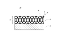
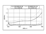
次に、参考として、第1実施形態に係る光学素子1に対する、第1比較例としての光学素子について説明する。図5は、第1実施形態に対する第1比較例に係る光学素子20の構成を示す概略断面図である。この図5において、第1実施形態に係る光学素子1の構成と同一のものには同一の符号を付し、説明を省略する。この光学素子20では、第1実施形態に係る低屈折率層3とは異なり、低屈折率層21は、中空微粒子4間の空隙がバインダー5で充填された1種類の膜からなる。まず、基材2は、第1実施形態と同一である。次に、低屈折率層21の屈折率が1.30になるように、中空SiO2含有溶液に対するバインダー溶液の重量比率を1:0.71として混合液を生成する。このとき、低屈折率層21では、上記のとおり中空微粒子4間の空隙がバインダー5で充填されるように、バインダー溶液の濃度が調整される。次に、第1実施形態と同様に、塗工処理および乾燥処理が実施され、基材2上に低屈折率層21を有する光学素子20が形成される。ここで、第1実施形態と同様に評価、観察した結果、図6に示すように、光学素子20によれば、第1実施形態に比べて反射率が高くなり、反射防止性能が劣ることが確認できる。これにより、第1実施形態に係る光学素子1の有用性が示される。なお、(表3)は、この光学素子20の構成に対する屈折率および膜厚を、基材2側から順に示す表である。
(First comparative example)
Next, as a reference, an optical element as a first comparative example with respect to the
(第2比較例)
さらに、参考として、第2実施形態に係る光学素子10に対する、第2比較例としての光学素子について説明する。図7は、第2実施形態に対する第2比較例に係る光学素子30の構成を示す概略断面図である。この図7において、第2実施形態に係る光学素子10の構成と同一のものには同一の符号を付し、説明を省略する。この光学素子30も、第2実施形態に係る光学素子10と同様に、多層反射防止膜31を含むものである。一方、多層反射防止膜31を構成する本比較例に係る低屈折率層32は、低屈折率層14とは異なり、中空微粒子4間の空隙がバインダー15で充填された1種類の膜からなる。まず、基材11は、第2実施形態と同一である。また、本比較例においても、多層反射防止膜31は、第2実施形態と同様に、5つの層で構成される多層膜33を含む。次に、低屈折率層32の屈折率が1.35になるように、中空SiO2含有溶液に対するバインダー溶液の重量比率を1:0.71として混合液を生成する。このとき、低屈折率層32では、上記のとおり中空微粒子4間の空隙がバインダー5で充填されるように、バインダー溶液の濃度が調整される。次に、第2実施形態と同様に、塗工処理および乾燥処理が実施され、基材11上に低屈折率層32を有する光学素子30が形成される。ここで、第2実施形態と同様に評価、観察した結果、図8に示すように、光学素子30によれば、第2実施形態に比べて反射率が高くなり、反射防止性能が劣ることが確認できる。これにより、第2実施形態に係る光学素子10の有用性が示される。なお、(表4)は、この光学素子30の構成に対する屈折率および膜厚を、基材11側から順に示す表である。
(Second comparative example)
Furthermore, as a reference, an optical element as a second comparative example with respect to the
(光学系および光学機器)
次に、本発明の一実施形態の光学系および光学機器について説明する。本実施形態の光学系は、例えば、ビデオカメラ、写真カメラ、またはテレビカメラなどの光学機器が備えるレンズ(光学素子)部、またはレンズ鏡筒の内部に構成される結像光学系である。この結像光学系は、光軸方向に並ぶ、少なくとも2つ以上のレンズを有し、例えば、光入射側から順に、接合レンズである第1レンズ、反射防止膜を有する第2レンズなどを含む。この第2レンズとして、上記実施形態にて説明した光学素子が採用可能である。本実施形態の光学系および光学機器によれば、従来よりも少なくとも結像性能の面で有利となる。
(Optical system and optical equipment)
Next, an optical system and an optical apparatus according to an embodiment of the present invention will be described. The optical system of the present embodiment is an imaging optical system configured inside a lens (optical element) unit or a lens barrel included in an optical device such as a video camera, a photographic camera, or a television camera, for example. The imaging optical system includes at least two or more lenses arranged in the optical axis direction, and includes, for example, a first lens that is a cemented lens and a second lens that has an antireflection film in order from the light incident side. . As the second lens, the optical element described in the above embodiment can be used. According to the optical system and the optical apparatus of the present embodiment, it is more advantageous at least in terms of imaging performance than the conventional one.
以上、本発明の好ましい実施形態について説明したが、本発明は、これらの実施形態に限定されず、その要旨の範囲内で種々の変形および変更が可能である。 As mentioned above, although preferable embodiment of this invention was described, this invention is not limited to these embodiment, A various deformation | transformation and change are possible within the range of the summary.
1 光学素子
2 基材
3 低屈折率層
3a 第1層
3b 第2層
4 中空微粒子
5 バインダー
DESCRIPTION OF
Claims (13)
前記反射防止膜は、複数の中空微粒子と、該中空微粒子を互いに結合するバインダーと、を有する低屈折率層を含み、
前記低屈折率層は、最表層としての第1層と、該第1層に隣接して前記基材の側に位置する第2層と、からなり、
前記第1層での前記バインダーの充填率は、前記第2層での前記バインダーの充填率よりも低く、
前記第1層での前記中空微粒子の充填率は、前記第2層での前記中空微粒子の充填率よりも低く、
前記第1層のd線に対する屈折率は、1.1以上1.25以下であり、
前記第1層は、前記バインダーの充填率が互いに異なる上層及び下層を含み、前記下層での前記バインダーの充填率は、前記第2層での前記バインダーの充填率よりも高いことを特徴とする光学素子。 An optical element having a base material and an antireflection film formed on the base material,
The antireflection film includes a low refractive index layer having a plurality of hollow fine particles and a binder that binds the hollow fine particles to each other,
The low refractive index layer comprises a first layer as an outermost layer, and a second layer located on the substrate side adjacent to the first layer,
The binder filling rate in the first layer is lower than the binder filling rate in the second layer,
The filling rate of the hollow fine particles in the first layer is lower than the filling rate of the hollow fine particles in the second layer,
The refractive index for the d-line of the first layer is 1.1 or more and 1.25 or less,
The first layer includes an upper layer and a lower layer having different binder filling rates, and the binder filling rate in the lower layer is higher than the binder filling rate in the second layer. Optical element.
Priority Applications (2)
| Application Number | Priority Date | Filing Date | Title |
|---|---|---|---|
| JP2011169008A JP6053262B2 (en) | 2011-08-02 | 2011-08-02 | Optical element, optical system and optical apparatus using the same |
| US13/549,573 US9417361B2 (en) | 2011-08-02 | 2012-07-16 | Optical element, and optical system and optical apparatus using same |
Applications Claiming Priority (1)
| Application Number | Priority Date | Filing Date | Title |
|---|---|---|---|
| JP2011169008A JP6053262B2 (en) | 2011-08-02 | 2011-08-02 | Optical element, optical system and optical apparatus using the same |
Publications (3)
| Publication Number | Publication Date |
|---|---|
| JP2013033124A JP2013033124A (en) | 2013-02-14 |
| JP2013033124A5 JP2013033124A5 (en) | 2014-09-11 |
| JP6053262B2 true JP6053262B2 (en) | 2016-12-27 |
Family
ID=47627117
Family Applications (1)
| Application Number | Title | Priority Date | Filing Date |
|---|---|---|---|
| JP2011169008A Active JP6053262B2 (en) | 2011-08-02 | 2011-08-02 | Optical element, optical system and optical apparatus using the same |
Country Status (2)
| Country | Link |
|---|---|
| US (1) | US9417361B2 (en) |
| JP (1) | JP6053262B2 (en) |
Families Citing this family (7)
| Publication number | Priority date | Publication date | Assignee | Title |
|---|---|---|---|---|
| US9372291B2 (en) * | 2013-11-04 | 2016-06-21 | Sung Nae CHO | Heat blocking system utilizing particulates |
| JP6274924B2 (en) | 2014-03-14 | 2018-02-07 | キヤノン株式会社 | Antireflection film, optical member, and method of manufacturing optical member |
| CN105208434A (en) * | 2014-06-11 | 2015-12-30 | 阿里巴巴集团控股有限公司 | Media projection method, media projection equipment, control terminal, and cloud server |
| TWI673513B (en) * | 2014-09-26 | 2019-10-01 | 日商大日本印刷股份有限公司 | Anti reflection film, display device, method for selecting anti reflection flim for display device |
| JP2017032781A (en) * | 2015-07-31 | 2017-02-09 | 富士フイルム株式会社 | Antireflection film, polarizing plate, cover glass, image display device, and method for manufacturing antireflection film |
| CN106680901B (en) * | 2015-11-11 | 2018-12-21 | 台湾创新材料股份有限公司 | 3-D ordered multiporous method for manufacturing microstructure |
| US20230110637A1 (en) | 2020-02-28 | 2023-04-13 | Nippon Sheet Glass Company, Limited | Low-refractive-index film, laminate, optical element, windbreak material, and display device |
Family Cites Families (11)
| Publication number | Priority date | Publication date | Assignee | Title |
|---|---|---|---|---|
| EP2226365B1 (en) * | 2001-10-25 | 2016-08-10 | Panasonic Intellectual Property Management Co., Ltd. | Panel light emitting body |
| JP4378972B2 (en) | 2003-02-25 | 2009-12-09 | パナソニック電工株式会社 | Antireflection film, method of manufacturing antireflection film, antireflection member |
| WO2005059601A1 (en) * | 2003-12-17 | 2005-06-30 | Bridgestone Corporation | Antireflection film, electromagnetic wave shielding light transmitting window material, gas discharge type light emitting panel, flat display panel, show window material and solar cell module |
| JP4497460B2 (en) * | 2004-06-11 | 2010-07-07 | Hoya株式会社 | Method for manufacturing antireflection film |
| JP5047488B2 (en) | 2004-11-05 | 2012-10-10 | ペンタックスリコーイメージング株式会社 | Method for producing silica airgel membrane |
| JP2007052345A (en) * | 2005-08-19 | 2007-03-01 | Oji Paper Co Ltd | Multilayered thin film structure with refractive index gradient and its manufacturing method |
| CN101086546A (en) * | 2006-06-09 | 2007-12-12 | 鸿富锦精密工业(深圳)有限公司 | Lens module and camera module |
| JP5339320B2 (en) * | 2006-09-01 | 2013-11-13 | Jsr株式会社 | Curable composition and antireflection film |
| TW200921139A (en) * | 2007-11-15 | 2009-05-16 | Daxon Technology Inc | Antiglare film and coating composition for antiglare films |
| JP2010160262A (en) * | 2009-01-07 | 2010-07-22 | Panasonic Corp | Antireflection structure, lens barrel equipped with the same, and method for manufacturing the antireflection structure |
| JP2009211078A (en) * | 2009-04-10 | 2009-09-17 | Hitachi Ltd | Antireflection film, image display device having the same, optical recording medium, solar power generation module, and method for forming antireflection film |
-
2011
- 2011-08-02 JP JP2011169008A patent/JP6053262B2/en active Active
-
2012
- 2012-07-16 US US13/549,573 patent/US9417361B2/en active Active
Also Published As
| Publication number | Publication date |
|---|---|
| JP2013033124A (en) | 2013-02-14 |
| US20130034711A1 (en) | 2013-02-07 |
| US9417361B2 (en) | 2016-08-16 |
Similar Documents
| Publication | Publication Date | Title |
|---|---|---|
| JP6053262B2 (en) | Optical element, optical system and optical apparatus using the same | |
| US20170285228A1 (en) | Optical member and method of producing the same | |
| JP5881096B2 (en) | Antireflection film and optical element | |
| JP5936444B2 (en) | Optical element, optical system and optical apparatus using the same | |
| CN104914488B (en) | Antireflection film, optical member, and method of producing optical member | |
| JP6903994B2 (en) | Optical element and its manufacturing method | |
| JP6292830B2 (en) | Optical element, optical system and optical apparatus | |
| US10168452B2 (en) | Antireflection coating, optical element, optical system and optical apparatus | |
| JP5885595B2 (en) | Antireflection film, and optical element, optical system, and optical apparatus having the same | |
| JP2017049313A (en) | Antireflection film, optical member, method of manufacturing antireflection film and method of manufacturing optical member | |
| JP6137807B2 (en) | Optical element having antireflection film, optical system and optical apparatus | |
| US20200308415A1 (en) | Optical member, optical device and coating liquid | |
| JP7343334B2 (en) | Lens unit and camera module | |
| JP6385108B2 (en) | Optical element and optical system, and method of manufacturing optical element | |
| JP7402669B2 (en) | Optical element with anti-reflection coating | |
| JP7405405B2 (en) | Anti-reflection film, optical element having same, and method for producing anti-reflection film | |
| JP2016085253A (en) | Anti-reflection film and optical element having the same | |
| JP6385117B2 (en) | Optical element and optical system having the same | |
| JP2014035415A (en) | Optical element and optical device having the same | |
| JP2016018095A (en) | Optical element, optical system, and optical equipment | |
| JP2016080943A (en) | Anti-reflection film and optical element | |
| JP2018025651A (en) | Optical device and optical system including the same, and imaging apparatus | |
| CN116931137A (en) | Article comprising porous layer containing inorganic particles and coating liquid for forming porous layer containing inorganic particles | |
| JP2015203723A5 (en) | ||
| JP2014174207A (en) | Antireflection film, and optical element and optical system having the same |
Legal Events
| Date | Code | Title | Description |
|---|---|---|---|
| A521 | Written amendment |
Free format text: JAPANESE INTERMEDIATE CODE: A523 Effective date: 20140728 |
|
| A621 | Written request for application examination |
Free format text: JAPANESE INTERMEDIATE CODE: A621 Effective date: 20140728 |
|
| A977 | Report on retrieval |
Free format text: JAPANESE INTERMEDIATE CODE: A971007 Effective date: 20150316 |
|
| A131 | Notification of reasons for refusal |
Free format text: JAPANESE INTERMEDIATE CODE: A131 Effective date: 20150407 |
|
| A521 | Written amendment |
Free format text: JAPANESE INTERMEDIATE CODE: A523 Effective date: 20150608 |
|
| A131 | Notification of reasons for refusal |
Free format text: JAPANESE INTERMEDIATE CODE: A131 Effective date: 20151110 |
|
| A521 | Written amendment |
Free format text: JAPANESE INTERMEDIATE CODE: A523 Effective date: 20160112 |
|
| A131 | Notification of reasons for refusal |
Free format text: JAPANESE INTERMEDIATE CODE: A131 Effective date: 20160517 |
|
| A521 | Written amendment |
Free format text: JAPANESE INTERMEDIATE CODE: A523 Effective date: 20160704 |
|
| TRDD | Decision of grant or rejection written | ||
| A01 | Written decision to grant a patent or to grant a registration (utility model) |
Free format text: JAPANESE INTERMEDIATE CODE: A01 Effective date: 20161101 |
|
| A61 | First payment of annual fees (during grant procedure) |
Free format text: JAPANESE INTERMEDIATE CODE: A61 Effective date: 20161129 |
|
| R151 | Written notification of patent or utility model registration |
Ref document number: 6053262 Country of ref document: JP Free format text: JAPANESE INTERMEDIATE CODE: R151 |