JP6042151B2 - Insulating material for semiconductor containing silica particles - Google Patents
Insulating material for semiconductor containing silica particles Download PDFInfo
- Publication number
- JP6042151B2 JP6042151B2 JP2012211345A JP2012211345A JP6042151B2 JP 6042151 B2 JP6042151 B2 JP 6042151B2 JP 2012211345 A JP2012211345 A JP 2012211345A JP 2012211345 A JP2012211345 A JP 2012211345A JP 6042151 B2 JP6042151 B2 JP 6042151B2
- Authority
- JP
- Japan
- Prior art keywords
- silica particles
- insulating material
- less
- measurement
- ratio
- Prior art date
- Legal status (The legal status is an assumption and is not a legal conclusion. Google has not performed a legal analysis and makes no representation as to the accuracy of the status listed.)
- Active
Links
Images


Landscapes
- Formation Of Insulating Films (AREA)
Description
本発明は、シリカ粒子を含む半導体用絶縁材料、等に関する。 The present invention relates to a semiconductor insulating material containing silica particles, and the like.
近年、メモリセルの集積度を高めるために、メモリセルを3次元的に配置した半導体記憶装置が多数提案されている。このような半導体装置において、メモリセル及び回路素子等の隙間にあたる箇所にトレンチを形成し、トレンチ内に絶縁材料を埋め込むことにより、メモリセル間及び回路素子間等の電気的分離を行う必要がある。このようなトレンチ埋め込み用絶縁材料としては、高い絶縁性が求められるという理由でシリコン酸化物が広く好適に用いられている。 In recent years, in order to increase the degree of integration of memory cells, many semiconductor memory devices in which memory cells are arranged three-dimensionally have been proposed. In such a semiconductor device, it is necessary to perform electrical isolation between the memory cells and between the circuit elements by forming a trench in a portion corresponding to a gap between the memory cell and the circuit element and embedding an insulating material in the trench. . As such an insulating material for filling a trench, silicon oxide is widely and preferably used because of its high insulating properties.
トレンチ内にシリコン酸化物を埋め込むための手段としては、従来CVD(化学気相成長)法が挙げられ、トレンチを有する基板上にシリコン酸化物膜を形成することができる。一方、CVD以外の方法として、塗布法により液状の材料をトレンチ内に埋設し、酸化雰囲気下で焼成することによりシリコン酸化物を形成する方法が知られている。この手法で用いる液状材料としては、ポリシラザン材料(例えば特許文献1)、ポリシラン材料(例えば特許文献2)、及びシリコーン材料が知られている。 As a means for embedding silicon oxide in the trench, there is a conventional CVD (chemical vapor deposition) method, and a silicon oxide film can be formed on a substrate having a trench. On the other hand, as a method other than CVD, a method of forming a silicon oxide by embedding a liquid material in a trench by a coating method and baking it in an oxidizing atmosphere is known. As liquid materials used in this method, polysilazane materials (for example, Patent Document 1), polysilane materials (for example, Patent Document 2), and silicone materials are known.
特にシリコーン材料は、塗布膜形成時に脱水及び脱アルコール縮合反応を伴うため、得られたシリコン酸化物膜中にボイド及びクラックが発生しやすい。またシリコーン材料からシリコン酸化物膜に転化する際に大きな硬化収縮を伴うため、膜表面からトレンチの底部に向かって密度が不均一になるといった問題があった。 In particular, since a silicone material is accompanied by dehydration and dealcohol condensation reactions when forming a coating film, voids and cracks are likely to occur in the obtained silicon oxide film. In addition, when the silicone material is converted into the silicon oxide film, there is a problem that the density becomes non-uniform from the film surface toward the bottom of the trench because of significant curing shrinkage.
このようなボイド及びクラックの発生を回避する方法として、シリカ粒子とポリシロキサン化合物とを含む組成物が提案されている(例えば特許文献3)。また、層間絶縁膜用途のために設計された材料として、シリカ粒子とポリシロキサン化合物とを縮合反応させた材料について特許文献4〜7に記載されている。
As a method for avoiding the occurrence of such voids and cracks, a composition containing silica particles and a polysiloxane compound has been proposed (for example, Patent Document 3).
さらにポリシロキサン化合物とシリカ粒子とを含む組成物は、塗布後、焼成して酸化シリコン膜とした時の硬化収縮率が小さく、HF耐性も示す材料であることが特許文献8、9に記載されている。 Further, Patent Documents 8 and 9 describe that a composition containing a polysiloxane compound and silica particles is a material having a low cure shrinkage ratio and a high resistance to HF when fired into a silicon oxide film after coating. ing.
半導体装置等の高集積化や多層化に伴い、メモリセル間及び回路素子間等を電気的分離するためにより優れた電気特性を示す材料が求められる。前述した優れた電気特性とはリーク電流が小さいことである。すなわち、本発明はリーク電流が小さい半導体用絶縁材料を提供することを目的とする。 As semiconductor devices and the like are highly integrated and multi-layered, materials that exhibit better electrical characteristics are required to electrically isolate memory cells and circuit elements. The above-described excellent electrical characteristics are low leakage current. That is, an object of the present invention is to provide a semiconductor insulating material with a small leakage current.
本発明者らは上記目的を達成する方法を開発すべく鋭意検討を行った結果、以下に示すようにシリカ粒子を特定の状態で含む絶縁材料がリーク電流を低減することを見出し、本発明を完成させた。即ち、本発明は以下の通りである。 As a result of intensive studies to develop a method for achieving the above object, the present inventors have found that an insulating material containing silica particles in a specific state reduces leakage current as shown below. Completed. That is, the present invention is as follows.
[1] 珪素原子、炭素原子、及び酸素原子を含む半導体用絶縁材料であって、
シリカ粒子を、9.5%より大きく30%以下である体積割合で含み、
炭素原子の珪素原子に対する組成比(C/Si)が0より大きく0.85より小さく、かつ
微小角入射X線小角散乱(GI−SAXS)測定における、散乱ベクトルqが0.1nm-1の時の散乱強度I1(q)の、該散乱ベクトルqが0.2nm-1の時の散乱強度I2(q)に対する比(I1(q)/I2(q))が、1.35以下である、半導体用絶縁材料。
[2] 前記炭素原子の珪素原子に対する組成比(C/Si)が0.54以上0.62以下である、上記[1]に記載の半導体用絶縁材料。
[3] 前記シリカ粒子の体積割合が13%以上20%以下である、上記[1]又は[2]に記載の半導体用絶縁材料。
[4] 上記[1]〜[3]のいずれかに記載の半導体用絶縁材料の製造方法であって、
ポリシロキサン化合物及びシリカ粒子を含む材料組成物を基板に塗布し、前記材料組成物を焼成硬化させる工程を含み、
前記ポリシロキサン化合物は、下記一般式(1):
R1Si(OR2)3 (1)
(式中、R1は炭素数1〜10の炭化水素基であり、そしてR2は各々独立に炭素数1〜6の炭化水素基である。)
で表される1種以上のシランモノマー及び下記一般式(2):
Si(OR3)4 (2)
(式中、R3は各々独立に炭素数1〜6の炭化水素基である。)
で表される1種以上のシランモノマーを合計で50質量%以上の量で含むシラン成分を加水分解重縮合することで得られる、半導体用絶縁材料の製造方法。
[5] 前記材料組成物が、前記ポリシロキサン化合物及び前記シリカ粒子の合計100質量部に対して前記シリカ粒子を20質量部以上30質量部以下含む、上記[4]に記載の半導体用絶縁材料の製造方法。
[1] A semiconductor insulating material containing a silicon atom, a carbon atom, and an oxygen atom,
Containing silica particles in a volume proportion of greater than 9.5% and not greater than 30%;
When the composition ratio (C / Si) of carbon atoms to silicon atoms is larger than 0 and smaller than 0.85, and the scattering vector q is 0.1 nm −1 in the small angle incident X-ray small angle scattering (GI-SAXS) measurement The ratio (I 1 (q) / I 2 (q)) of the scattering intensity I 1 (q) to the scattering intensity I 2 (q) when the scattering vector q is 0.2 nm −1 is 1.35. An insulating material for semiconductor, which is the following.
[2] The semiconductor insulating material according to [1], wherein the composition ratio (C / Si) of the carbon atom to the silicon atom is 0.54 or more and 0.62 or less.
[3] The semiconductor insulating material according to the above [1] or [2], wherein a volume ratio of the silica particles is 13% or more and 20% or less.
[4] A method for producing an insulating material for a semiconductor according to any one of [1] to [3],
Applying a material composition containing a polysiloxane compound and silica particles to a substrate, and baking and curing the material composition;
The polysiloxane compound has the following general formula (1):
R 1 Si (OR 2 ) 3 (1)
(Wherein R 1 is a hydrocarbon group having 1 to 10 carbon atoms, and R 2 is each independently a hydrocarbon group having 1 to 6 carbon atoms.)
One or more silane monomers represented by the following general formula (2):
Si (OR 3 ) 4 (2)
(In the formula, each R 3 is independently a hydrocarbon group having 1 to 6 carbon atoms.)
The manufacturing method of the insulating material for semiconductors obtained by carrying out hydrolysis polycondensation of the silane component which contains the 1 or more types of silane monomer represented by these in the quantity of 50 mass% or more in total.
[5] The semiconductor insulating material according to [4], wherein the material composition includes 20 parts by mass or more and 30 parts by mass or less of the silica particles with respect to 100 parts by mass in total of the polysiloxane compound and the silica particles. Manufacturing method.
本発明により、リーク電流を低減可能な、シリカ粒子を含む半導体用絶縁材料を提供できる。 According to the present invention, it is possible to provide a semiconductor insulating material containing silica particles that can reduce leakage current.
以下、本発明を実施するための形態(以下、「実施の形態」と略記する)について詳細に説明する。尚、本発明は、以下の実施の形態に限定されるものではなく、その要旨の範囲内で種々変形して実施することができる。 Hereinafter, modes for carrying out the present invention (hereinafter abbreviated as “embodiments”) will be described in detail. In addition, this invention is not limited to the following embodiment, It can implement by changing variously within the range of the summary.
本発明の半導体用絶縁材料(以下、単に絶縁材料ということもある)は、炭素原子、珪素原子及び酸素原子を含み、典型的には炭素原子、珪素原子及び酸素原子並びに不可避的不純物からなる。絶縁材料は、シリカ粒子を含み、以下の(1)、(2)及び(3)の特徴を満足する。
(1) 炭素原子の珪素原子に対する組成比(C/Si)(本開示で、C/Si比ともいう)(原子数比)が0より大きく0.85より小さい。
(2) シリカ粒子の体積割合が9.5%より大きく30%以下である。
(3) 微小角入射X線小角散乱(GI−SAXS)において、散乱ベクトルqが0.1nm-1の時の散乱強度I1(q)の、散乱ベクトルqが0.2nm-1の時の散乱強度I2(q)に対する比(I1(q)/I2(q))が1.35以下である。
The insulating material for a semiconductor of the present invention (hereinafter sometimes referred to simply as an insulating material) contains a carbon atom, a silicon atom, and an oxygen atom, and typically comprises a carbon atom, a silicon atom, an oxygen atom, and an unavoidable impurity. The insulating material contains silica particles and satisfies the following characteristics (1), (2) and (3).
(1) The composition ratio (C / Si) of carbon atoms to silicon atoms (also referred to as C / Si ratio in the present disclosure) (atomic number ratio) is greater than 0 and less than 0.85.
(2) The volume fraction of silica particles is greater than 9.5% and not greater than 30%.
(3) In small-angle incident X-ray small angle scattering (GI-SAXS), the scattering intensity I 1 (q) when the scattering vector q is 0.1 nm −1 and the scattering vector q when the scattering vector q is 0.2 nm −1 The ratio (I 1 (q) / I 2 (q)) to the scattering intensity I 2 (q) is 1.35 or less.
<(3)に関して>
本発明の絶縁材料は微小角入射X線小角散乱(GI−SAXS)において、散乱ベクトルqが0.1nm-1の時の散乱強度I1(q)の、散乱ベクトルqが0.2nm-1の時の散乱強度I2(q)に対する比(I1(q)/I2(q))が1.35以下であることを特徴とする。ここで散乱ベクトルqはq=4πsinθ/λであり、2θは散乱角度、λは入射X線の波長である。散乱強度I(q)は散乱体積中の電子密度の揺らぎに関係しており、I(q)から、ナノスケールの周期構造、並びに散乱体の形及び大きさを知ることができる。本発明の絶縁材料は、炭素原子、珪素原子及び酸素原子を含み、かつシリカ粒子を含んでいる。従って、絶縁材料において、シリカ粒子(すなわち珪素原子と酸素原子とからなる部分)とシリカ粒子以外の部分(すなわち炭素原子を少なくとも含む部分)とは電子密度差を有する。例えば、絶縁材料は、有機基を含む珪素化合物(例えば後述のポリシロキサン化合物)を用いて製造でき、この場合、シリカ粒子以外の部分は有機基由来の炭素を含むことになり、シリカ粒子の部分とシリカ粒子以外の部分とは顕著な電子密度差を有する。よって、GI−SAXSで観察される散乱の殆どは、シリカ粒子の粒径及び粒子の分布状態(すなわち配置)に由来すると考えられる。以上により、本実施の形態では、GI−SAXS測定により、シリカ粒子の存在状態を評価する。
<Regarding (3)>
Insulating material of the present invention in Grazing Incidence X-ray small angle scattering (GI-SAXS), the scattering intensity when the scattering vector q is 0.1nm -1 I 1 (q), the scattering vector q is 0.2 nm -1 The ratio (I 1 (q) / I 2 (q)) to the scattering intensity I 2 (q) at this time is 1.35 or less. Here, the scattering vector q is q = 4π sin θ / λ, 2θ is the scattering angle, and λ is the wavelength of the incident X-ray. The scattering intensity I (q) is related to the fluctuation of the electron density in the scattering volume, and the nanoscale periodic structure and the shape and size of the scatterer can be known from I (q). The insulating material of the present invention contains carbon atoms, silicon atoms, and oxygen atoms, and contains silica particles. Accordingly, in the insulating material, the silica particles (that is, the portion composed of silicon atoms and oxygen atoms) and the portion other than the silica particles (that is, the portion including at least carbon atoms) have an electron density difference. For example, the insulating material can be manufactured using a silicon compound containing an organic group (for example, a polysiloxane compound described later). In this case, the portion other than the silica particles contains carbon derived from the organic group, and the silica particle portion And portions other than the silica particles have a significant difference in electron density. Therefore, it is considered that most of the scattering observed with GI-SAXS is derived from the particle size of the silica particles and the distribution state (ie, arrangement) of the particles. As described above, in the present embodiment, the presence state of silica particles is evaluated by GI-SAXS measurement.
GI−SAXS測定における0.5nm-1以下の小角領域の測定からは、シリカ粒子の凝集の度合いに関する情報を得ることができる。材料中のシリカ粒子を剛体球とみなし、シリカ粒子が材料中に均一に存在していると仮定したモデルで解析を行うと、散乱ベクトルqが0.1nm-1から0.2nm-1の小角領域における散乱強度I(q)の変化は小さい。実際、散乱ベクトルqが0.1nm-1の時の散乱強度I1(q)の、該qが0.2nm-1の時の散乱強度I2(q)に対する比(I1(q)/I2(q))は1.35以下となる。すなわち、シリカ粒子を含むある材料についての測定結果がこのモデルに近い場合、シリカ粒子はその材料中に均一に存在しており、凝集は起こっていないと考えることができる。一方、散乱ベクトルqが0.1nm-1の時の散乱強度I1(q)が、該qが0.2nm-1の時の散乱強度I2(q)よりも非常に大きくなる場合、シリカ粒子が材料中に均一に存在していない、すなわち粒子間での相互作用による凝集が起こっていると考えることができる。 Information on the degree of aggregation of silica particles can be obtained from measurement of a small-angle region of 0.5 nm −1 or less in GI-SAXS measurement. When the silica particle in the material is regarded as a hard sphere and the analysis is performed with a model assuming that the silica particle exists uniformly in the material, the small angle of the scattering vector q from 0.1 nm −1 to 0.2 nm −1 The change in the scattering intensity I (q) in the region is small. In fact, the scattering intensity when the scattering vector q is 0.1 nm -1 I 1 of (q), the ratio of scattering intensity I 2 (q) when the said q is 0.2nm -1 (I 1 (q) / I 2 (q)) is 1.35 or less. That is, when the measurement result of a certain material containing silica particles is close to this model, it can be considered that the silica particles are uniformly present in the material and no aggregation occurs. On the other hand, when the scattering intensity I 1 (q) when the scattering vector q is 0.1 nm −1 is much larger than the scattering intensity I 2 (q) when q is 0.2 nm −1 , silica It can be considered that the particles are not uniformly present in the material, that is, aggregation occurs due to the interaction between the particles.
発明者は、散乱ベクトルqが0.1nm-1の時の散乱強度I1(q)の、該qが0.2nm-1の時の散乱強度I2(q)に対する比(I1(q)/I2(q))が1.35以下である条件を満たさない絶縁材料である場合、リーク電流が劇的に増加することを見出した。おそらくシリカ粒子の凝集が顕著となり、それが絶縁材料中の欠陥となった結果、リーク電流が生じやすくなるためと考えられる。以上より、本実施の形態の絶縁材料において、散乱ベクトルqが0.1nm-1の時の散乱強度I1(q)の、該qが0.2nm-1の時の散乱強度I2(q)に対する比(I1(q)/I2(q))が1.35以下である必要がある。 Inventors, the scattering intensity when the scattering vector q is 0.1 nm -1 I 1 of (q), the ratio of scattering intensity I 2 (q) when the said q is 0.2nm -1 (I 1 (q It was found that the leakage current increases dramatically when the insulating material does not satisfy the condition that) / I 2 (q)) is 1.35 or less. Probably, the aggregation of silica particles becomes prominent, and this is a defect in the insulating material. As a result, leakage current is likely to occur. From the above, the insulating material of the present embodiment, the scattering intensity when the scattering vector q is 0.1 nm -1 I 1 of (q), the scattering intensity I 2 (q when the said q is 0.2 nm -1 ) (I 1 (q) / I 2 (q)) must be 1.35 or less.
さらにシリカ粒子の凝集を抑制するという観点で、前述したI1(q)/I2(q)が1.30以下であることがより好ましく、更に好ましくは1.20以下である。I1(q)/I2(q)比は、シリカ粒子の凝集を抑制するという観点では小さい程好ましいが、粒子が膜中に均一に存在しているモデルに近いという観点から、好ましくは0以上、より好ましくは0.25以上、更に好ましくは0.50以上であることができる。 Further, from the viewpoint of suppressing aggregation of silica particles, I 1 (q) / I 2 (q) described above is more preferably 1.30 or less, and still more preferably 1.20 or less. The I 1 (q) / I 2 (q) ratio is preferably as small as possible from the viewpoint of suppressing the aggregation of silica particles, but is preferably 0 from the viewpoint of being close to a model in which the particles are uniformly present in the film. More preferably, it can be 0.25 or more, more preferably 0.50 or more.
本発明におけるGI−SAXS測定では2次元検出器を用いる。2次元検出器を用いることは時間分割測定や異方性の把握において優位である。ただし、2次元検出器ではビームパスで生じる空気散乱すべてを計測してしまうため、真空若しくはヘリウムガス中での測定が必要である。 In the GI-SAXS measurement in the present invention, a two-dimensional detector is used. The use of a two-dimensional detector is advantageous in time division measurement and grasping of anisotropy. However, since the two-dimensional detector measures all air scattering generated in the beam path, measurement in a vacuum or helium gas is necessary.
また上記測定では、2次元GI−SAXSパターンに対し、試料面内の散乱のみを取り出し、これを1次元化する。これにより小角領域における散乱強度を正確に測定することができ、本発明における散乱強度比(I1(q)/I2(q))を適切に算出することが可能となる。 In the above measurement, only the scattering within the sample surface is taken out from the two-dimensional GI-SAXS pattern and is made one-dimensional. As a result, the scattering intensity in the small-angle region can be accurately measured, and the scattering intensity ratio (I 1 (q) / I 2 (q)) in the present invention can be appropriately calculated.
絶縁材料は、より典型的には、限定はされないが、例えば、温度20℃以上25℃以下、相対湿度40%以上50%以下の条件下で、シリカ粒子を含む材料組成物の基材上への塗布及び続いて焼成炉内での焼成により作製される。更に典型的には、絶縁材料は、後述の実施例において記載する条件で作製される。 The insulating material is more typically, but not limited to, for example, onto a substrate of a material composition containing silica particles under conditions of a temperature of 20 ° C. to 25 ° C. and a relative humidity of 40% to 50%. And subsequent baking in a baking furnace. More typically, the insulating material is made under the conditions described in the examples below.
上記したような特定のI1(q)/I2(q)比を満足する絶縁材料は、シリカ粒子とポリシロキサン化合物を重縮合させ、得られる材料組成物を焼成硬化させることにより形成できる。その際、絶縁材料中のシリカ粒子の体積割合を所定値以下にすることが重要である。詳細は後述する。 An insulating material satisfying the specific I 1 (q) / I 2 (q) ratio as described above can be formed by polycondensation of silica particles and a polysiloxane compound and baking and curing the resulting material composition. At that time, it is important to set the volume ratio of the silica particles in the insulating material to a predetermined value or less. Details will be described later.
<(1)に関して>
半導体用途の絶縁膜のために設計された従来の材料に関し、有機基を含むポリシロキサンを含む材料組成物を用いて形成される絶縁材料は、一般的な絶縁材料であるSiO2のみでは困難とされているクラック耐性、低収縮性、及び疎水性を示す。それらの特性は絶縁材料中における炭素/珪素組成比に大きく依存しうるため、炭素/珪素組成比の決定は極めて重要である。
<Regarding (1)>
With respect to conventional materials designed for insulating films for semiconductor applications, insulating materials formed using a material composition containing polysiloxane containing organic groups are difficult only with SiO 2 which is a general insulating material. It exhibits crack resistance, low shrinkage, and hydrophobicity. Since these characteristics can largely depend on the carbon / silicon composition ratio in the insulating material, the determination of the carbon / silicon composition ratio is extremely important.
本発明の絶縁材料は、C/Si比が0より大きく0.85より小さいことを特徴とする。該C/Si比が0より大きいことは、膜の疎水性を高め、吸着水によるリーク電流を低減する点で有利である。該C/Si比は好ましくは0.28以上、更に好ましくは0.54以上である。一方、該C/Si比が0.85より小さいことはシリカ粒子の凝集を抑制し、リーク電流を低減する点で有利である。該C/Si比は好ましくは0.75以下、より好ましくは、0.62以下である。上記C/Si比はX線光電子分光法(XPS)により測定することができる。本発明におけるXPS測定は従来公知の方法及び装置を用いて行えばよい。またC/Si比を測定する上で、ラザフォード後方散乱分析法(RBS)、核反応分析法(NRA)等他の測定手法を用いてもよく、当業者に公知のいずれかの方法で上記範囲内のC/Si比が得られればよい。 The insulating material of the present invention is characterized in that the C / Si ratio is larger than 0 and smaller than 0.85. When the C / Si ratio is larger than 0, it is advantageous in that the hydrophobicity of the film is increased and the leakage current due to adsorbed water is reduced. The C / Si ratio is preferably 0.28 or more, more preferably 0.54 or more. On the other hand, when the C / Si ratio is less than 0.85, it is advantageous from the viewpoint of suppressing aggregation of silica particles and reducing leakage current. The C / Si ratio is preferably 0.75 or less, more preferably 0.62 or less. The C / Si ratio can be measured by X-ray photoelectron spectroscopy (XPS). The XPS measurement in the present invention may be performed using a conventionally known method and apparatus. In measuring the C / Si ratio, other measurement methods such as Rutherford backscattering analysis (RBS) and nuclear reaction analysis (NRA) may be used. It is sufficient that the C / Si ratio is obtained.
絶縁材料は、より典型的には、限定はされないが、例えば、温度20℃以上25℃以下、相対湿度40%以上50%以下の条件下で、シリカ粒子を含む材料組成物の基材上への塗布及び続いて焼成炉内での焼成により作製される。更に典型的には、絶縁材料は、後述の実施例において記載する条件で作製される。 The insulating material is more typically, but not limited to, for example, onto a substrate of a material composition containing silica particles under conditions of a temperature of 20 ° C. to 25 ° C. and a relative humidity of 40% to 50%. And subsequent baking in a baking furnace. More typically, the insulating material is made under the conditions described in the examples below.
上記したような特定のC/Si比を満足する絶縁材料は、シリカ粒子とポリシロキサン化合物を重縮合させ、得られる材料組成物を焼成硬化させることにより形成できる。その際、材料組成物におけるポリシロキサン化合物とシリカ粒子との割合、ポリシロキサン化合物中の有機基の炭素数(例えば、後述する一般式(1)及び(2)で表されるシランモノマーにおける炭化水素基の炭素数)を選定することが重要である。 The insulating material satisfying the specific C / Si ratio as described above can be formed by polycondensing silica particles and a polysiloxane compound, and baking and curing the resulting material composition. At that time, the ratio of the polysiloxane compound and the silica particles in the material composition, the carbon number of the organic group in the polysiloxane compound (for example, the hydrocarbon in the silane monomer represented by the following general formulas (1) and (2)) It is important to select the number of carbon groups.
<(2)に関して>
本発明の絶縁材料は、材料中のシリカ粒子とその他の成分との体積割合の総和を100%とすると、シリカ粒子の体積割合は9.5%より大きく30%以下であることを特徴とする。上記したGI−SAXS測定における0.5nm-1以上の広角領域の測定からは、シリカ粒子の分布状態、すなわち絶縁材料中のシリカ粒子の体積割合に関する情報を得ることができる。本開示のシリカ粒子の体積割合は以下のように定義される。すなわち、SAXS測定における散乱ベクトル(q)が0.5nm-1以上の広角領域における散乱強度プロファイルを、シリカ粒子を剛体球と仮定したときの種々のシリカ粒子体積割合のモデルによる散乱強度プロファイルでフィッティングし、実測プロファイルと一致するモデルプロファイルのシリカ粒子体積割合を、本開示のシリカ粒子の体積割合とする。
シリカ粒子の体積割合が9.5%より大きいことはリーク電流を低減する点で有利である。該体積割合は好ましくは11%以上、より好ましくは13%以上である。一方、該体積割合が30%以下であることはシリカ粒子の凝集を抑制し、リーク電流を低減する点で有利である。該体積割合は好ましくは25%以下、より好ましくは20%以下である。
<Regarding (2)>
The insulating material of the present invention is characterized in that the volume ratio of the silica particles is larger than 9.5% and not more than 30%, assuming that the total volume ratio of the silica particles and other components in the material is 100%. . Information on the distribution state of the silica particles, that is, the volume ratio of the silica particles in the insulating material can be obtained from the measurement in the wide-angle region of 0.5 nm −1 or more in the above-described GI-SAXS measurement. The volume ratio of the silica particles of the present disclosure is defined as follows. That is, the scattering intensity profile in the wide-angle region where the scattering vector (q) in the SAXS measurement is 0.5 nm −1 or more is fitted with the scattering intensity profiles based on various silica particle volume ratio models when the silica particles are assumed to be hard spheres. Then, the silica particle volume ratio of the model profile that matches the actual measurement profile is defined as the volume ratio of the silica particles of the present disclosure.
The volume ratio of silica particles being larger than 9.5% is advantageous in terms of reducing leakage current. The volume ratio is preferably 11% or more, more preferably 13% or more. On the other hand, the volume ratio of 30% or less is advantageous in that the aggregation of silica particles is suppressed and the leakage current is reduced. The volume ratio is preferably 25% or less, more preferably 20% or less.
シリカ粒子としては、例えば、ヒュームドシリカ、コロイダルシリカ等が挙げられる。上記ヒュームドシリカは、ケイ素原子を含む化合物を気相中で酸素及び水素と反応させることによって得ることができる。原料となるケイ素化合物としては、例えば、ハロゲン化ケイ素(例えば塩化ケイ素等)等が挙げられる。 Examples of the silica particles include fumed silica and colloidal silica. The fumed silica can be obtained by reacting a compound containing a silicon atom with oxygen and hydrogen in a gas phase. Examples of the silicon compound used as a raw material include silicon halide (for example, silicon chloride).
上記コロイダルシリカは、原料化合物を加水分解・縮合するゾルゲル法により合成することができる。コロイダルシリカの原料としては、例えば、アルコキシケイ素(例えばテトラエトキシシラン等)、ハロゲン化シラン化合物(例えばジフェニルジクロロシラン等)等が挙げられる。これらの中でも、金属イオン、ハロゲン等の不純物の混入が少ないという観点から、アルコキシケイ素から得られるコロイダルシリカが好ましい。 The colloidal silica can be synthesized by a sol-gel method in which a raw material compound is hydrolyzed and condensed. Examples of the raw material for colloidal silica include alkoxy silicon (for example, tetraethoxysilane) and halogenated silane compounds (for example, diphenyldichlorosilane). Among these, colloidal silica obtained from alkoxy silicon is preferable from the viewpoint that impurities such as metal ions and halogens are not mixed.
シリカ粒子の平均一次粒子径は、1nm以上120nm以下であることが好ましく、より好ましくは、1nm以上40nm以下、更に好ましくは、1nm以上20nm以下、最も好ましくは、1nm以上15nm以下である。上記平均一次粒径が1nm以上である場合、耐クラック性が良好であり、120nm以下である場合、トレンチへの埋め込み性が良好である。 The average primary particle diameter of the silica particles is preferably 1 nm to 120 nm, more preferably 1 nm to 40 nm, still more preferably 1 nm to 20 nm, and most preferably 1 nm to 15 nm. When the average primary particle size is 1 nm or more, the crack resistance is good, and when it is 120 nm or less, the embedding property in the trench is good.
シリカ粒子の平均二次粒子径は、2nm以上250nm以下であることが好ましく、より好ましくは2nm以上80nm以下、更に好ましくは2nm以上40nm以下、最も好ましくは2nm以上30nm以下である。上記平均二次粒径が2nm以上である場合、耐クラック性が良好であり、250nm以下である場合トレンチへの埋め込み性が良好である。 The average secondary particle diameter of the silica particles is preferably 2 nm to 250 nm, more preferably 2 nm to 80 nm, still more preferably 2 nm to 40 nm, and most preferably 2 nm to 30 nm. When the average secondary particle size is 2 nm or more, the crack resistance is good, and when it is 250 nm or less, the embedding property in the trench is good.
上記平均一次粒子径は、窒素分子の圧力と吸着量とから算出される比表面積(BET法)により求められる。また、上記平均二次粒子径は、動的光散乱光度計により測定される。 The average primary particle diameter is determined by a specific surface area (BET method) calculated from the pressure and adsorption amount of nitrogen molecules. The average secondary particle diameter is measured with a dynamic light scattering photometer.
前述の(1)〜(3)の特徴を満足する絶縁材料は、典型的には、シリカ粒子及びシリコン酸化物を含む絶縁材料であって、該シリコン酸化物が、ポリシロキサン化合物の焼成によって得られるものである。
好ましい態様において、該ポリシロキサン化合物は、下記一般式(1):
R1Si(OR2)3 (1)
(式中、R1は炭素数1〜10の炭化水素基であり、そしてR2は各々独立に炭素数1〜6の炭化水素基である。)
で表される1種以上のシランモノマー及び下記一般式(2):
Si(OR3)4 (2)
(式中、R3は各々独立に炭素数1〜6の炭化水素基である。)
で表される1種以上のシランモノマーを合計で好ましくは50質量%以上の量で含むシラン成分を、加水分解重縮合することで得られる。
The insulating material satisfying the above features (1) to (3) is typically an insulating material containing silica particles and silicon oxide, and the silicon oxide is obtained by firing a polysiloxane compound. It is what
In a preferred embodiment, the polysiloxane compound has the following general formula (1):
R 1 Si (OR 2 ) 3 (1)
(Wherein R 1 is a hydrocarbon group having 1 to 10 carbon atoms, and R 2 is each independently a hydrocarbon group having 1 to 6 carbon atoms.)
One or more silane monomers represented by the following general formula (2):
Si (OR 3 ) 4 (2)
(In the formula, each R 3 is independently a hydrocarbon group having 1 to 6 carbon atoms.)
It is obtained by hydrolytic polycondensation of a silane component containing one or more silane monomers represented by the formulas in a total amount of preferably 50% by mass or more.
絶縁材料のシリカ粒子以外の部分は、炭素原子を、原子数基準で、好ましくは10%以上、より好ましくは15%以上、更に好ましくは20%以上、また好ましくは35%以下、より好ましくは30%以下、更に好ましくは25%以下含有する。
絶縁材料のシリカ粒子以外の部分は、珪素原子を、原子数基準で、好ましくは15%以上、より好ましくは20%以上、更に好ましくは25%以上、また好ましくは45%以下、より好ましくは40%以下、更に好ましくは35%以下含有する。
絶縁材料のシリカ粒子以外の部分は、酸素原子を、原子数基準で、好ましくは35%以上、より好ましくは40%以上、更に好ましくは45%以上、また好ましくは60%以下、より好ましくは55%以下、更に好ましくは50%以下含有する。
これらの含有量は絶縁材料のXPS測定より得られる炭素、珪素、酸素の元素数比からシリカ粒子(SiO2)の体積割合分の寄与を除いて算出される値である。
The portion other than the silica particles of the insulating material preferably contains 10% or more, more preferably 15% or more, still more preferably 20% or more, and preferably 35% or less, more preferably 30% of carbon atoms based on the number of atoms. % Or less, more preferably 25% or less.
The portion other than the silica particles of the insulating material preferably contains silicon atoms on the basis of the number of atoms, preferably 15% or more, more preferably 20% or more, still more preferably 25% or more, and preferably 45% or less, more preferably 40%. % Or less, more preferably 35% or less.
The portion other than the silica particles of the insulating material preferably has an oxygen atom of 35% or more, more preferably 40% or more, still more preferably 45% or more, and preferably 60% or less, more preferably 55, based on the number of atoms. % Or less, more preferably 50% or less.
These contents are values calculated by excluding the contribution of the volume fraction of silica particles (SiO 2 ) from the ratio of the number of carbon, silicon, and oxygen elements obtained by XPS measurement of the insulating material.
<絶縁材料の製造方法>
本実施の形態はまた、シリカ粒子を含む材料組成物を基板に塗布して塗布基板を得る塗布工程と、該塗布工程で得た塗布基板を加熱する焼成工程とを含む絶縁材料の製造方法を提供する。
好ましい態様は、半導体用絶縁材料の製造方法であって、
ポリシロキサン化合物及びシリカ粒子を含む材料組成物を基板に塗布し、該材料組成物を焼成硬化させる工程を含み、
該ポリシロキサン化合物は、下記一般式(1):
R1Si(OR2)3 (1)
(式中、R1は炭素数1〜10の炭化水素基であり、そしてR2は各々独立に炭素数1〜6の炭化水素基である。)
で表される1種以上のシランモノマー及び下記一般式(2):
Si(OR3)4 (2)
(式中、R3は各々独立に炭素数1〜6の炭化水素基である。)
で表される1種以上のシランモノマーを合計で50質量%以上の量で含むシラン成分を加水分解重縮合することで得られる、半導体用絶縁材料の製造方法を提供する。
<Insulating material manufacturing method>
The present embodiment also provides an insulating material manufacturing method including a coating step of applying a material composition containing silica particles to a substrate to obtain a coated substrate, and a baking step of heating the coated substrate obtained in the coating step. provide.
A preferred embodiment is a method for producing an insulating material for a semiconductor,
Applying a material composition comprising a polysiloxane compound and silica particles to a substrate and baking and curing the material composition;
The polysiloxane compound has the following general formula (1):
R 1 Si (OR 2 ) 3 (1)
(Wherein R 1 is a hydrocarbon group having 1 to 10 carbon atoms, and R 2 is each independently a hydrocarbon group having 1 to 6 carbon atoms.)
One or more silane monomers represented by the following general formula (2):
Si (OR 3 ) 4 (2)
(In the formula, each R 3 is independently a hydrocarbon group having 1 to 6 carbon atoms.)
The manufacturing method of the insulating material for semiconductors obtained by carrying out the hydrolysis polycondensation of the silane component which contains the 1 or more types of silane monomer represented by these in the quantity of 50 mass% or more in total is provided.
シリカ粒子を含む材料組成物は、通常の方法で基板上に塗布することができる。塗布方法としては、例えば、スピンコート法、ディップコート法、ローラーブレード塗布法、スプレー塗布法等が挙げられる。これらの中でも、成膜時の塗布膜厚みが均一であるという点から、スピンコート法が好ましい。 The material composition containing silica particles can be applied onto the substrate by a usual method. Examples of the coating method include spin coating, dip coating, roller blade coating, and spray coating. Among these, the spin coating method is preferable from the viewpoint that the thickness of the coating film during film formation is uniform.
上記基板としては、例えば、シリコン基板が挙げられる。また基板としてはトレンチ構造を有するものを使用することができる。例えば、トレンチ構造を有するシリコン基板にスピンコート法によって材料組成物を塗布する場合、1段階での回転数で塗布しても、複数段階の回転数を組み合わせて塗布しても構わない。少なくとも1段階目の回転数を低速にし、2段階目以降を高速にすることが好ましい。1段階目に低速で回転させることによって材料組成物をシリコン基板の全面に広げることができ、埋め込み性が良好になる。また、材料組成物の塗布回数は1回でも複数回でも構わないが、成膜性が良好であるという観点及び製造コストが低減できるという観点から、1回で塗布することが好ましい。 An example of the substrate is a silicon substrate. A substrate having a trench structure can be used. For example, when a material composition is applied to a silicon substrate having a trench structure by a spin coating method, it may be applied at a single rotation speed or a combination of multiple rotation speeds. It is preferable to set the rotational speed of at least the first stage to a low speed and to increase the speed of the second and subsequent stages. By rotating at a low speed in the first stage, the material composition can be spread over the entire surface of the silicon substrate, and the embedding property is improved. Further, the number of times of application of the material composition may be one or more, but it is preferable to apply the material composition at a time from the viewpoint of good film formability and a reduction in manufacturing cost.
上記塗布工程において、基板上に塗布する材料組成物の固形分濃度については特に制限はなく、目的とする塗布膜の膜厚に合わせて任意の固形分濃度で実施できる。 In the coating step, the solid content concentration of the material composition to be coated on the substrate is not particularly limited, and can be carried out at any solid content concentration according to the target film thickness of the coating film.
上記塗布工程の温度及び時間については特に制限はないが、温度は0℃以上100℃以下であることが好ましく、より好ましくは20℃以上80℃以下であり、時間は、0.1分以上30分以下であることが好ましく、より好ましくは0.2分以上10分以下である。 Although there is no restriction | limiting in particular about the temperature and time of the said application | coating process, It is preferable that temperature is 0 to 100 degreeC, More preferably, it is 20 to 80 degreeC, Time is 0.1 to 30 minutes. It is preferably not more than minutes, more preferably not less than 0.2 minutes and not more than 10 minutes.
次いで、焼成工程において上記塗布基板を加熱する。なお、上記塗布工程において、材料組成物を基板上に塗布した後、塗布膜中の残留溶媒を除くために50℃〜200℃の範囲で予備硬化(プリベーク)させることが好ましい。このとき、段階的に温度を上げても、連続的に温度を上げてもよい。予備硬化(プリベーク)時の雰囲気は、酸素、水蒸気等の酸化性ガスを含む酸化性雰囲気であっても、酸化性ガスを実質的に含まない非酸化性雰囲気であっても構わない。 Next, the coated substrate is heated in the firing step. In the above coating step, it is preferable to pre-cure (pre-bake) the material composition in a range of 50 ° C. to 200 ° C. after removing the residual solvent in the coating film after coating the material composition on the substrate. At this time, the temperature may be raised stepwise or continuously. The atmosphere at the time of pre-curing (pre-baking) may be an oxidizing atmosphere containing an oxidizing gas such as oxygen or water vapor, or a non-oxidizing atmosphere substantially not containing an oxidizing gas.
次いで、任意に予備硬化(プリベーク)させて得られた膜を加熱焼成することによって硬化膜を得ることができる。加熱焼成の方法としては、例えば、ホットプレート、オーブン、ファーネス等の一般的な加熱手段を適用することができる。加熱焼成は非酸化性雰囲気で行うことが好ましい。加熱焼成温度は、200℃以上900℃以下であることが好ましく、より好ましくは300℃以上800℃以下、更に好ましくは350℃以上750℃以下である。加熱焼成温度が200℃以上であれば、得られる膜質が良好であり、900℃以下であれば、耐クラック性が良好である。 Next, a cured film can be obtained by heating and baking a film obtained by optionally pre-curing (pre-baking). As a heating and baking method, for example, a general heating means such as a hot plate, an oven, or a furnace can be applied. Heating and baking are preferably performed in a non-oxidizing atmosphere. The heating and baking temperature is preferably 200 ° C. or higher and 900 ° C. or lower, more preferably 300 ° C. or higher and 800 ° C. or lower, and further preferably 350 ° C. or higher and 750 ° C. or lower. If the heating and baking temperature is 200 ° C. or higher, the obtained film quality is good, and if it is 900 ° C. or lower, the crack resistance is good.
上記非酸化性雰囲気とは、例えば、真空下、又は窒素、ヘリウム、アルゴン、キセノン等の不活性雰囲気が挙げられる。これらの不活性雰囲気中に含まれる、酸素、水蒸気等の酸化性ガスの濃度は1000ppm以下であることが好ましく、より好ましくは100ppm以下、更に好ましくは10ppm以下である。非酸化性雰囲気の圧力については特に制限は無く、加圧、常圧、又は減圧のいずれでもよい。 Examples of the non-oxidizing atmosphere include a vacuum or an inert atmosphere such as nitrogen, helium, argon, or xenon. The concentration of an oxidizing gas such as oxygen or water vapor contained in these inert atmospheres is preferably 1000 ppm or less, more preferably 100 ppm or less, and further preferably 10 ppm or less. There is no restriction | limiting in particular about the pressure of a non-oxidizing atmosphere, Any of pressurization, a normal pressure, or pressure reduction may be sufficient.
上記焼成工程において、700℃以上900℃以下の高温領域では、水素を含む気体中で加熱焼成を行うことが好ましい。焼成工程で使用する水素を含む気体は、焼成工程の初期から、即ち、基板温度が700℃未満である時点から導入してもよいし、700℃に到達してから導入してもよい。更に、一旦700℃以上900℃以下の温度で水素を含まない気体で第1の加熱を行った後に、水素を含む気体を導入して第2の加熱を行うという2段階で加熱焼成を行ってもよい。いずれの方法でも、加熱焼成を終えた基板が400℃以下の温度、好ましくは室温程度に冷却されるまで、水素を含む気体を導入したままにしておくことが好ましい。 In the baking step, it is preferable to perform heat baking in a gas containing hydrogen in a high temperature region of 700 ° C. or higher and 900 ° C. or lower. The gas containing hydrogen used in the firing process may be introduced from the beginning of the firing process, that is, from the time when the substrate temperature is lower than 700 ° C., or may be introduced after reaching 700 ° C. Furthermore, after performing the first heating with a gas not containing hydrogen at a temperature of 700 ° C. or more and 900 ° C. or less, the heating and firing are performed in two stages, in which a gas containing hydrogen is introduced and the second heating is performed. Also good. In any method, it is preferable to keep introducing a gas containing hydrogen until the substrate after heating and baking is cooled to a temperature of 400 ° C. or lower, preferably about room temperature.
上述のように、焼成工程を、水素を含む気体中で行うことは、上記一般式(1)で表されるシラン及び上記一般式(2)で表されるシランを用いる場合に特に有利である。すなわちこの場合、シリコン原子と有機基との間の化学結合が700℃を超える高温で切断されても、発生するダングリングボンドを水素で終端することができるため、シラノール基の形成を防止し、半導体素子の絶縁材料として良好な膜物性を実現することが可能となる。 As described above, performing the firing step in a gas containing hydrogen is particularly advantageous when the silane represented by the general formula (1) and the silane represented by the general formula (2) are used. . That is, in this case, even if the chemical bond between the silicon atom and the organic group is broken at a high temperature exceeding 700 ° C., the generated dangling bond can be terminated with hydrogen, thereby preventing the formation of a silanol group, It is possible to realize good film properties as an insulating material of a semiconductor element.
焼成工程における熱処理時間は、好ましくは1分以上24時間以下であり、より好ましくは30分以上12時間以下である。 The heat treatment time in the firing step is preferably 1 minute to 24 hours, and more preferably 30 minutes to 12 hours.
焼成工程においては、酸化性雰囲気での加熱焼成と光処理とを併用しても構わない。加熱と光処理とを同時に行う場合の温度は、20℃以上600℃以下であることが好ましく、処理時間は、0.1分以上120分以下であることが好ましい。光処理には、例えば、可視光線、紫外線、遠紫外線等を使用できる。光処理の光源としては、例えば、低圧若しくは高圧の水銀ランプ、重水素ランプ、又はアルゴン、クリプトン、キセノン等の希ガスの放電光、YAGレーザー、アルゴンレーザー、炭酸ガスレーザー、又はXeF、XeCl、XeBr、KrF、KrCl、ArF若しくはArCl等のエキシマレーザー等を使用することができる。これらの光源の出力は、10〜5,000Wであることが好ましい。 In the firing step, heat firing in an oxidizing atmosphere and light treatment may be used in combination. The temperature when heating and light treatment are performed simultaneously is preferably 20 ° C. or more and 600 ° C. or less, and the treatment time is preferably 0.1 minutes or more and 120 minutes or less. For the light treatment, for example, visible light, ultraviolet light, deep ultraviolet light, or the like can be used. As a light source for light treatment, for example, a low-pressure or high-pressure mercury lamp, deuterium lamp, or discharge light of a rare gas such as argon, krypton, or xenon, YAG laser, argon laser, carbon dioxide gas laser, or XeF, XeCl, XeBr Excimer lasers such as KrF, KrCl, ArF or ArCl can be used. The output of these light sources is preferably 10 to 5,000 W.
これらの光源の光の波長は、基板上に形成された、シリカ粒子を含む材料組成物の膜によって少しでも吸収があればよく、170nm以上600nm以下であることが好ましい。光処理において、光の照射量は、0.1J/cm2以上1,000J/cm2以下であることが好ましく、より好ましくは1J/cm2以上100J/cm2以下である。また、光処理と同時にオゾンを発生させても構わない。上述した条件で光処理することによって、基板上に形成した膜において、シリカ粒子を含む材料組成物の酸化反応が進行し、焼成後の膜質を向上させることができる。 The light wavelength of these light sources may be absorbed as much as possible by the film of the material composition containing silica particles formed on the substrate, and is preferably 170 nm or more and 600 nm or less. In light treatment, a light irradiation amount is preferably at 0.1 J / cm 2 or more 1,000 J / cm 2 or less, more preferably 1 J / cm 2 or more 100 J / cm 2 or less. Moreover, ozone may be generated simultaneously with the light treatment. By performing the light treatment under the conditions described above, the oxidation reaction of the material composition containing silica particles proceeds in the film formed on the substrate, and the film quality after baking can be improved.
材料組成物がポリシロキサン化合物を含む場合、上記焼成工程の後に、絶縁材料の表面を疎水化処理剤にさらしても構わない。硬化膜を疎水化処理剤にさらすことで、該硬化膜中のシラノール基と疎水化処理剤とが反応し、硬化膜の表面を疎水化することができる。 When the material composition includes a polysiloxane compound, the surface of the insulating material may be exposed to a hydrophobizing agent after the baking step. By exposing the cured film to a hydrophobizing agent, the silanol groups in the cured film react with the hydrophobizing agent, and the surface of the cured film can be hydrophobized.
<シリカ粒子を含む材料組成物の製造>
シリカ粒子を含む材料組成物の好ましい製造方法について以下に説明する。
本発明におけるシリカ粒子を含む材料組成物は、好ましくは、下記一般式(1):
R1Si(OR2)3 (1)
(式中、R1は炭素数1〜10の炭化水素基であり、そしてR2は各々独立に炭素数1〜6の炭化水素基である。)
で表される1種以上のシランモノマー及び下記一般式(2):
Si(OR3)4 (2)
(式中、R3は各々独立に炭素数1〜6の炭化水素基である。)
で表される1種以上のシランモノマーを含むシラン成分を加水分解重縮合することで得られるポリシロキサン化合物と、シリカ粒子とを含む組成物である。
<Manufacture of material composition containing silica particles>
A preferred method for producing a material composition containing silica particles will be described below.
The material composition containing silica particles in the present invention is preferably the following general formula (1):
R 1 Si (OR 2 ) 3 (1)
(Wherein R 1 is a hydrocarbon group having 1 to 10 carbon atoms, and R 2 is each independently a hydrocarbon group having 1 to 6 carbon atoms.)
One or more silane monomers represented by the following general formula (2):
Si (OR 3 ) 4 (2)
(In the formula, each R 3 is independently a hydrocarbon group having 1 to 6 carbon atoms.)
It is a composition containing the polysiloxane compound obtained by carrying out hydrolysis polycondensation of the silane component containing 1 or more types of silane monomers represented by these, and a silica particle.
上記一般式(1)において、R1は炭素数1〜10の炭化水素基であり、非環式及び環式の飽和脂肪族炭化水素基、芳香族炭化水素基、非環式及び環式の不飽和脂肪族炭化水素基、並びにこれらの2つ以上の組合せの基(例えばアリールアルキル基)等が挙げられる。 In the general formula (1), R 1 is a hydrocarbon group having 1 to 10 carbon atoms, and acyclic and cyclic saturated aliphatic hydrocarbon groups, aromatic hydrocarbon groups, acyclic and cyclic groups. Examples thereof include an unsaturated aliphatic hydrocarbon group, and a combination of two or more of these (for example, an arylalkyl group).
この中でも、焼成時のシリコン酸化物への転化の際に重量減少が少なく、収縮率が小さいポリシロキサン化合物を与えることができるという観点から、R1はメチル基又はエチル基であることが好ましく、より好ましくはメチル基である。 Among these, R 1 is preferably a methyl group or an ethyl group from the viewpoint of providing a polysiloxane compound having a small weight loss upon conversion to silicon oxide during firing and having a small shrinkage rate. More preferably, it is a methyl group.
上記一般式(1)及び(2)において、R2及びR3は各々独立に炭素数1〜6の炭化水素基である。炭素数1〜6の炭化水素基としては、メチル基、エチル基、n−プロピル基、iso−プロピル基、n−ブチル基、t−ブチル基、n−ヘキシル基、シクロヘキシル基等が挙げられる。 In the general formulas (1) and (2), R 2 and R 3 are each independently a hydrocarbon group having 1 to 6 carbon atoms. Examples of the hydrocarbon group having 1 to 6 carbon atoms include a methyl group, an ethyl group, an n-propyl group, an iso-propyl group, an n-butyl group, a t-butyl group, an n-hexyl group, and a cyclohexyl group.
この中でも、反応性制御の容易さという観点から、R2及びR3はそれぞれメチル基又はエチル基であることが好ましい。 Among these, from the viewpoint of easy reactivity control, R 2 and R 3 are each preferably a methyl group or an ethyl group.
上記ポリシロキサン化合物は、上記シランモノマー(1)及び上記シランモノマー(2)をそれぞれ1種以上含むシラン成分を加水分解重縮合して得られるものであればよく、数種類のシランモノマーを組み合わせて用いてもよい。用いるシランモノマーの組み合わせは、目的とするポリシロキサン化合物の物性に合わせて選択することが可能である。一般的に、官能基数が少ないシランモノマーを用いることにより、重合度が高く靱性に優れたポリシロキサン化合物が得られ、官能基数が多いシランモノマーを用いることにより、緻密で機械強度の高いポリシロキサン化合物が得られる。 The polysiloxane compound only needs to be obtained by hydrolytic polycondensation of silane components each containing one or more of the silane monomer (1) and the silane monomer (2). A combination of several silane monomers is used. May be. The combination of silane monomers to be used can be selected according to the physical properties of the target polysiloxane compound. In general, by using a silane monomer having a small number of functional groups, a polysiloxane compound having a high degree of polymerization and excellent toughness can be obtained, and by using a silane monomer having a large number of functional groups, a dense and high mechanical strength polysiloxane compound. Is obtained.
このような観点から、半導体素子に用いる絶縁材料としては、上記一般式(1)で表されるシランモノマーに加え、上記一般式(2)で表されるシランモノマーを適宜組み合わせて用いることがより好ましい。 From such a viewpoint, as the insulating material used for the semiconductor element, in addition to the silane monomer represented by the general formula (1), the silane monomer represented by the general formula (2) is appropriately used in combination. preferable.
一般式(1)で表されるシランモノマー(以下、シランモノマー(1)ともいう)と一般式(2)で表されるシランモノマー(以下、シランモノマー(2)ともいう)との混合比は、モル比で、0/100〜100/0まで可能であるが、耐クラック性の観点から、シランモノマー(1)/シランモノマー(2)(モル比)は、30/70〜90/10であることが好ましい。より好ましくは、上記モル比が50/50〜85/15であり、更に好ましくは70/30〜80/20である。シラン成分は、シランモノマー(1)及びシランモノマー(2)以外のモノマーを含んでも含まなくてもよく、典型的には含まない。 The mixing ratio of the silane monomer represented by the general formula (1) (hereinafter also referred to as silane monomer (1)) and the silane monomer represented by the general formula (2) (hereinafter also referred to as silane monomer (2)) is The molar ratio is 0/100 to 100/0. From the viewpoint of crack resistance, the silane monomer (1) / silane monomer (2) (molar ratio) is 30/70 to 90/10. Preferably there is. More preferably, the molar ratio is 50/50 to 85/15, and more preferably 70/30 to 80/20. The silane component may or may not contain a monomer other than the silane monomer (1) and the silane monomer (2), and typically does not contain it.
シラン成分中、シランモノマー(1)とシランモノマー(2)との合計含有率は、耐クラック性を良好に得る観点から、好ましくは50質量%以上、より好ましくは70質量%以上、更に好ましくは90質量%以上であり、最も典型的には100質量%である。 In the silane component, the total content of the silane monomer (1) and the silane monomer (2) is preferably 50% by mass or more, more preferably 70% by mass or more, and still more preferably from the viewpoint of obtaining good crack resistance. 90% by mass or more, and most typically 100% by mass.
ポリシロキサン化合物中での上記モル比は、例えば、1H−NMR及び29Si−NMRを用いて確認することができる。 The molar ratio in the polysiloxane compound can be confirmed using, for example, 1 H-NMR and 29 Si-NMR.
上記ポリシロキサン化合物は、上記シラン成分を従来公知の方法を用いて加水分解重縮合することによって製造できる。加水分解重縮合の典型的な手法としては、酸触媒、水存在下でシラン成分を反応させる手法が挙げられる。 The polysiloxane compound can be produced by hydrolytic polycondensation of the silane component using a conventionally known method. A typical technique for hydrolysis polycondensation is a technique of reacting a silane component in the presence of an acid catalyst and water.
シリカ粒子を含む材料組成物中のシリカ粒子の含有率は、前記ポリシロキサン化合物及び前記シリカ粒子の合計100質量部に対して、好ましくは16質量部以上34質量部以下、より好ましくは20質量部以上30質量部以下である。リーク電流を低減させる観点で、シリカ粒子の上記含有率は16質量部以上であることが好ましい。また材料組成物中のシリカ粒子の凝集を抑制するという観点で上記含有率は34質量部以下であることが好ましい。なお本開示において、ポリシロキサン化合物及びシリカ粒子の合計を100質量部とするときのポリシロキサン化合物の量としては、縮合換算量(すなわち、ポリシロキサン化合物中に残存する加水分解性基(具体的には、一般式(1)中のOR2及び一般式(2)中のOR3)をそれぞれ1/2個のOで置き換えた量を用いる。 The content of silica particles in the material composition containing silica particles is preferably 16 parts by mass or more and 34 parts by mass or less, more preferably 20 parts by mass with respect to 100 parts by mass in total of the polysiloxane compound and the silica particles. The amount is 30 parts by mass or less. From the viewpoint of reducing the leakage current, the content of the silica particles is preferably 16 parts by mass or more. Moreover, it is preferable that the said content rate is 34 mass parts or less from a viewpoint of suppressing aggregation of the silica particle in a material composition. In the present disclosure, the amount of the polysiloxane compound when the total of the polysiloxane compound and the silica particles is 100 parts by mass is the amount in terms of condensation (that is, the hydrolyzable group remaining in the polysiloxane compound (specifically, Are used in such a manner that OR 2 in the general formula (1) and OR 3 in the general formula (2) are each replaced with 1/2 O.
材料組成物において、シリカ粒子は、上記ポリシロキサン化合物と単に混合された状態で存在してもよく、また、ポリシロキサン化合物と縮合した状態で存在(ポリシロキサン化合物と、シリカ粒子とが縮合した縮合成分を含有)していてもよい。材料組成物が、上記シリカ粒子と上記ポリシロキサン化合物との縮合反応物を含む場合、耐クラック性が特に良好な絶縁材料を形成できる。 In the material composition, the silica particles may exist in a state of being simply mixed with the polysiloxane compound, or may be present in a state of being condensed with the polysiloxane compound (condensation in which the polysiloxane compound and the silica particles are condensed). Component). When the material composition contains a condensation reaction product of the silica particles and the polysiloxane compound, an insulating material with particularly good crack resistance can be formed.
ポリシロキサン化合物とシリカ粒子との縮合反応物の製造方法としては、以下のような方法が挙げられる。
(i)上記シランモノマー(1)及び上記シランモノマー(2)を含むシラン成分を加水分解重縮合反応させてポリシロキサン化合物を製造した後に、シリカ粒子と得られたポリシロキサン化合物とを更に縮合反応させる方法。
(ii)上記シランモノマー(1)及び上記シランモノマー(2)を含むシラン成分を加水分解重縮合反応させる際に、シリカ粒子を共存させておく方法。
(iii)上記シランモノマー(1)及び上記シランモノマー(2)を含むシラン成分を加水分解重縮合反応させている途中に、シリカ粒子を反応系に添加する方法。
Examples of a method for producing a condensation reaction product of a polysiloxane compound and silica particles include the following methods.
(I) A polysiloxane compound is produced by hydrolytic polycondensation reaction of the silane component including the silane monomer (1) and the silane monomer (2), and then the silica particles and the obtained polysiloxane compound are further subjected to a condensation reaction. How to make.
(Ii) A method in which silica particles are allowed to coexist when the silane component containing the silane monomer (1) and the silane monomer (2) is subjected to a hydrolysis polycondensation reaction.
(Iii) A method in which silica particles are added to the reaction system during the hydrolysis polycondensation reaction of the silane component containing the silane monomer (1) and the silane monomer (2).
シリカ粒子を上記ポリシロキサン化合物又は上記シラン成分と反応させる際には、溶媒に分散した状態の材料を反応させることができる。使用される溶媒としては、水若しくは有機溶媒又はこれらの混合溶媒を使用することができる。使用される有機溶媒としては、水若しくは有機溶媒又はこれらの混合溶媒を使用することができる。使用される有機溶媒は使用されるシリカ粒子の分散媒によって変わる。使用されるシリカ粒子の分散媒が水系の場合は、水若しくはアルコール系溶媒をシリカ粒子の水系分散媒に加えてからポリシロキサン化合物又はシラン成分とシリカ粒子との反応を行ってもよいし、シリカ粒子の水系溶液を一度アルコール系溶媒に置換してから、ポリシロキサン化合物又はシラン成分とシリカ粒子との反応を行ってもよい。使用できるアルコール溶媒としては、例えばメタノール、エタノール、n−プロパノール、2−プロパノール、n−ブタノール、メトキシエタノール、エトキシエタノール等が挙げられ、これらは水と容易に混合するため好ましい。 When the silica particles are reacted with the polysiloxane compound or the silane component, a material dispersed in a solvent can be reacted. As a solvent to be used, water, an organic solvent, or a mixed solvent thereof can be used. As the organic solvent used, water, an organic solvent, or a mixed solvent thereof can be used. The organic solvent used varies depending on the dispersion medium of the silica particles used. When the silica particle dispersion medium used is aqueous, the reaction between the polysiloxane compound or the silane component and the silica particles may be carried out after adding water or an alcohol solvent to the silica particle aqueous dispersion medium. The aqueous solution of the particles may be replaced with an alcohol solvent once, and then the reaction between the polysiloxane compound or the silane component and the silica particles may be performed. Examples of the alcohol solvent that can be used include methanol, ethanol, n-propanol, 2-propanol, n-butanol, methoxyethanol, ethoxyethanol, and the like, and these are preferable because they are easily mixed with water.
シリカ粒子とポリシロキサン化合物又はシラン成分とを反応させる際の反応温度に特に制限はなく、通常50℃から200℃の範囲で行われる。 There is no restriction | limiting in particular in the reaction temperature at the time of making a silica particle react with a polysiloxane compound or a silane component, Usually, it carries out in 50 to 200 degreeC.
材料組成物は、ポリシロキサン化合物、シリカ粒子及びこれらの縮合反応物以外の成分、例えば、窒素含有化合物等の添加剤、溶媒等を含んでいても構わない。添加剤としては、目的に合わせた添加剤を任意に選択できる。添加剤の使用量は、添加剤が効果を発揮し、且つ材料組成物の他の物性、例えば、揮発成分量等に影響を与えない範囲が好ましい。添加剤は、直接添加しても、適切な溶媒で希釈した溶液として添加してもよい。 The material composition may contain components other than the polysiloxane compound, silica particles and their condensation reaction products, for example, additives such as nitrogen-containing compounds, solvents, and the like. As the additive, an additive suitable for the purpose can be arbitrarily selected. The amount of the additive used is preferably within a range in which the additive exhibits an effect and does not affect other physical properties of the material composition, such as the amount of volatile components. The additive may be added directly or as a solution diluted with an appropriate solvent.
シリカ粒子を含む材料組成物が溶媒を含有する場合、溶媒としては、例えば、アルコール、ケトン、エステル、エーテル及び炭化水素溶媒から選ばれる1種類以上の溶媒が挙げられる。これらの溶媒の沸点は100℃以上200℃以下であることが好ましい。 When the material composition containing silica particles contains a solvent, examples of the solvent include one or more solvents selected from alcohols, ketones, esters, ethers, and hydrocarbon solvents. The boiling point of these solvents is preferably 100 ° C. or higher and 200 ° C. or lower.
次に、実施例及び比較例によって本実施の形態をより詳細に説明する。本実施の形態はこれらに限定されるものではない。 Next, the present embodiment will be described in more detail with reference to examples and comparative examples. The present embodiment is not limited to these.
<評価方法>
[縮合反応物の重量平均分子量(Mw)の測定]
プロピレングリコールモノメチルエチルアセテート(PGMEA)溶液である材料組成物を、縮合反応物の濃度が1質量%になるようにテトラヒドロフラン(THF)で希釈して、ゲルパーミエーションクロマトグラフィー(GPC)で測定した。重量平均分子量(Mw)は、標準物質であるポリエチレングリコール(PEG)換算の値として求めた。
(GPC測定条件)
・GPCシステム:SCL−1APvp(島津製作所社製)
・カラム:Shodex KF−804L(昭和電工株式会社)2本直列
・溶離液:THF(流量:1mL/min)
・カラム使用温度:40℃
<Evaluation method>
[Measurement of weight average molecular weight (Mw) of condensation reaction product]
A material composition which was a propylene glycol monomethyl ethyl acetate (PGMEA) solution was diluted with tetrahydrofuran (THF) so that the concentration of the condensation reaction product was 1% by mass, and measured by gel permeation chromatography (GPC). The weight average molecular weight (Mw) was determined as a value in terms of polyethylene glycol (PEG) as a standard substance.
(GPC measurement conditions)
・ GPC system: SCL-1APvp (manufactured by Shimadzu Corporation)
Column: Shodex KF-804L (Showa Denko Co., Ltd.) 2 in series Eluent: THF (flow rate: 1 mL / min)
Column operating temperature: 40 ° C
[膜評価項目]
(1)X線光電子分光(XPS)測定
(測定試料作製)
Si基板に材料組成物をスピンコートにより塗布して成膜した後、100℃で2分間、続いて140℃で5分間、ホットプレート上で段階的にプリベークした。その後、600℃、酸素濃度10ppm以下の雰囲気下で焼成することで厚さ100nm程度の絶縁膜を得た。
(スピンコート条件)
・スピンコーター:Mark−8
・メイン回転数:1600rpm
(1000rpm×10秒+1000rpm×30秒+799rpm×10秒)
・メイン回転時間:40秒
(XPS測定)
サーモフィッシャーESCALAB250を用い、以下の条件で測定を実施した。
(測定条件)
・励起源:mono.AlKα 15kVx10mA
・分析サイズ:約1mm(形状は楕円)
・Survey scan:0−1100eV
・Narrow scan:Si2p,C1s
・Pass Energy
Survey scan:100eV ; Narrow scan:20eV
測定で得られたナロースペクトルから得られる相対元素濃度から炭素/珪素組成比(C/Si)を計算した。
[Film evaluation items]
(1) X-ray photoelectron spectroscopy (XPS) measurement (measurement sample preparation)
The material composition was applied onto a Si substrate by spin coating to form a film, and then prebaked stepwise on a hot plate at 100 ° C. for 2 minutes and then at 140 ° C. for 5 minutes. Then, an insulating film having a thickness of about 100 nm was obtained by firing in an atmosphere at 600 ° C. and an oxygen concentration of 10 ppm or less.
(Spin coating conditions)
・ Spin coater: Mark-8
・ Main rotation speed: 1600rpm
(1000 rpm × 10 seconds + 1000 rpm × 30 seconds + 799 rpm × 10 seconds)
・ Main rotation time: 40 seconds (XPS measurement)
The measurement was carried out under the following conditions using a thermo-fischer ESCALAB250.
(Measurement condition)
Excitation source: mono. AlKα 15kVx10mA
・ Analysis size: about 1mm
・ Survey scan: 0-1100eV
・ Narrow scan: Si2p, C1s
・ Pass Energy
Survey scan: 100 eV; Narrow scan: 20 eV
The carbon / silicon composition ratio (C / Si) was calculated from the relative element concentration obtained from the narrow spectrum obtained by the measurement.
(2)微小角入射X線小角散乱(GI−SAXS)測定
(測定試料作製)
Si基板に材料組成物をスピンコートにより塗布して成膜した後、100℃で2分間、続いて140℃で5分間、ホットプレート上で段階的にプリベークした。その後、600℃、酸素濃度10ppm以下の雰囲気下で焼成することで、厚さ400nm程度の絶縁膜を得た。これを3cm角に切り出したものを測定試料とした。
・スピンコーター:Mark−8
・メイン回転数:1600rpm
(1600rpm×10秒+1600rpm×30秒+799rpm×10秒)
・メイン回転時間:40秒
(GI−SAXS測定と評価)
GI−SAXS測定はSPring−8のBL03XUにて行った。実験の詳細を以下に記す。
GI−SAXSにはX線波長1nmの入射X線を用い、検出器にはイメージングプレート(リガク製R−AXIS IV)を用いた。試料へのX線入射は入射X線と試料面のなす角が0.14°になるように調整した。測定中は雰囲気を真空とし、測定温度は室温とした。2次元GI−SAXSパターンに対しては試料面内の散乱のみを取り出し、これを1次元化した。得られた測定データ中の散乱ベクトル(q)が0.1nm-1の時の散乱強度I1(q)の、該qが0.2nm-1の時の散乱強度I2(q)に対する比(I1(q)/I2(q))が1.35以下である場合を○、1.35より大きい場合は×とした。
材料中のシリカ粒子の体積割合は以下の方法で求めた。得られた測定データの散乱ベクトル(q)が0.5nm-1以上の広角領域のプロファイルを、シリカ粒子を剛体球と仮定した、種々のシリカ粒子体積割合のモデルのプロファイルでフィッティングし、実測プロファイルと一致するモデルプロファイルのシリカ粒子体積割合をサンプルにおけるシリカ粒子の体積割合とした。
(2) Small angle incident X-ray small angle scattering (GI-SAXS) measurement (measurement sample preparation)
The material composition was applied onto a Si substrate by spin coating to form a film, and then prebaked stepwise on a hot plate at 100 ° C. for 2 minutes and then at 140 ° C. for 5 minutes. Thereafter, firing was performed in an atmosphere at 600 ° C. and an oxygen concentration of 10 ppm or less to obtain an insulating film having a thickness of about 400 nm. A sample cut into a 3 cm square was used as a measurement sample.
・ Spin coater: Mark-8
・ Main rotation speed: 1600rpm
(1600 rpm x 10 seconds + 1600 rpm x 30 seconds + 799 rpm x 10 seconds)
・ Main rotation time: 40 seconds (GI-SAXS measurement and evaluation)
GI-SAXS measurement was performed with BL03XU of SPring-8. Details of the experiment are described below.
An incident X-ray having an X-ray wavelength of 1 nm was used for GI-SAXS, and an imaging plate (R-AXIS IV manufactured by Rigaku) was used for the detector. The X-ray incidence to the sample was adjusted so that the angle formed by the incident X-ray and the sample surface was 0.14 °. During the measurement, the atmosphere was evacuated and the measurement temperature was room temperature. For the two-dimensional GI-SAXS pattern, only scattering within the sample surface was taken out and made one-dimensional. Of scattering intensity I 1 at the time of the resulting scattering vector in measurement data (q) is 0.1 nm -1 (q), the ratio of scattering intensity I 2 (q) when the said q is 0.2 nm -1 The case where (I 1 (q) / I 2 (q)) was 1.35 or less was marked as ◯, and the case where it was larger than 1.35 was marked as x.
The volume ratio of silica particles in the material was determined by the following method. Fitting the profile of the wide angle region where the scattering vector (q) of the obtained measurement data is 0.5 nm -1 or more with the profile of various silica particle volume ratios assuming that the silica particle is a hard sphere, the measured profile The volume ratio of the silica particles in the sample was the volume ratio of the silica particles in the model profile that coincided with.
(3)電気特性評価
(測定試料作製)
p型低抵抗Si基板に材料組成物をスピンコートにより塗布して成膜した後、100℃で2分間、続いて140℃で5分間、ホットプレート上で段階的にプリベークした。その後、600℃、酸素濃度10ppm以下の雰囲気下で焼成することで厚さ100nm程度の絶縁膜を得た。
(スピンコート条件)
・スピンコーター:Mark−8
・メイン回転数:1600rpm
(1000rpm×10秒+1000rpm×30秒+799rpm×10秒)
・メイン回転時間:40秒
次に絶縁膜表面及びSi基板裏面に厚み約250nmのアルミニウムを真空蒸着してキャパシタを作製した。このとき絶縁膜表面にはマスクを介して、半径1mmの円形の上部電極を形成した。
(電気特性評価)
I−V測定にはAgilent社製AgilentB1500A半導体デバイス・アナライザ、Micromanipulator社製プローバー装置を用いた。電界強度が−3.5MV/cmの時の電流密度をリーク電流値とし、値が1.0x10-6A/cm2以下である場合を○、1.0x10-6A/cm2よりも大きい場合を×とした。
(3) Electrical property evaluation (measurement sample preparation)
The material composition was applied onto a p-type low-resistance Si substrate by spin coating to form a film, and then pre-baked stepwise on a hot plate at 100 ° C. for 2 minutes and then at 140 ° C. for 5 minutes. Then, an insulating film having a thickness of about 100 nm was obtained by firing in an atmosphere at 600 ° C. and an oxygen concentration of 10 ppm or less.
(Spin coating conditions)
・ Spin coater: Mark-8
・ Main rotation speed: 1600rpm
(1000 rpm × 10 seconds + 1000 rpm × 30 seconds + 799 rpm × 10 seconds)
Main rotation time: 40 seconds Next, a capacitor was fabricated by vacuum-depositing aluminum having a thickness of about 250 nm on the surface of the insulating film and the back surface of the Si substrate. At this time, a circular upper electrode having a radius of 1 mm was formed on the surface of the insulating film through a mask.
(Electrical characteristics evaluation)
For the IV measurement, Agilent B1500A semiconductor device analyzer manufactured by Agilent, and a prober apparatus manufactured by Micromanipulator were used. The current density when the electric field strength is −3.5 MV / cm is defined as a leakage current value, and when the value is 1.0 × 10 −6 A / cm 2 or less, ○, larger than 1.0 × 10 −6 A / cm 2 The case was marked with x.
[実施例1]
還流管、滴下ロート、及び攪拌機を備えた500mLセパラブルフラスコに、メチルトリメトキシシラン(MTMS)22.2g、テトラエトキシシラン(TEOS)8.9g、及びエタノール61.9gを加え、撹拌しながら内温75℃まで昇温した。0.7質量%硝酸水溶液1.9gとイオン交換水20.3gとの混合物を滴下しながら加え、滴下後、75℃で2時間攪拌した。その後エタノール103.1gを加え、水分散シリカ粒子(PL−06、扶桑化学工業株式会社製、平均一次粒径6nm、6.0質量%濃度)55.5gを滴下した。滴下後、内温80℃まで昇温した。4時間後加熱を止めて室温まで放冷し、反応混合物を得た。
[Example 1]
To a 500 mL separable flask equipped with a reflux tube, a dropping funnel, and a stirrer, 22.2 g of methyltrimethoxysilane (MTMS), 8.9 g of tetraethoxysilane (TEOS), and 61.9 g of ethanol were added and stirred. The temperature was raised to 75 ° C. A mixture of 1.9 g of a 0.7% by mass nitric acid aqueous solution and 20.3 g of ion-exchanged water was added dropwise, followed by stirring at 75 ° C. for 2 hours. Thereafter, 103.1 g of ethanol was added, and 55.5 g of water-dispersed silica particles (PL-06, manufactured by Fuso Chemical Industry Co., Ltd., average primary particle size 6 nm, 6.0 mass% concentration) were added dropwise. After dropping, the temperature was raised to an internal temperature of 80 ° C. After 4 hours, heating was stopped and the mixture was allowed to cool to room temperature to obtain a reaction mixture.
上記反応混合物を1Lフラスコに移し、プロピレングリコールメチルエチルアセテート(PGMEA)300gを添加し、エバポレーターでエタノール及び水を除去し、材料組成物A−1を得た(固形分濃度18質量%のPGMEA溶液。材料組成物の固形分中のシリカ粒子は20質量%)。得られた材料組成物A−1のMwは1805であった。 The above reaction mixture was transferred to a 1 L flask, 300 g of propylene glycol methyl ethyl acetate (PGMEA) was added, ethanol and water were removed by an evaporator, and a material composition A-1 was obtained (PGMEA solution having a solid content concentration of 18% by mass) 20% by mass of silica particles in the solid content of the material composition). Mw of obtained material composition A-1 was 1805.
得られた材料組成物A−1を前述のように焼成硬化させて得た膜に関して、XPS測定、GI−SAXS測定、及び電気特性評価を行った。GI−SAXS測定から得られた膜中のシリカ粒子の体積割合は13%であった。XPS測定から得られた炭素/珪素原子組成比(C/Si)は0.62であった。GI−SAXS測定から得られた散乱強度比I1(q)/I2(q)は0.90であった。電界強度が−3.5MV/cmの時のリーク電流は8.2x10-7A/cm2であった。 XPS measurement, GI-SAXS measurement, and electrical property evaluation were performed on the film obtained by baking and curing the obtained material composition A-1 as described above. The volume ratio of the silica particles in the film obtained from the GI-SAXS measurement was 13%. The carbon / silicon atom composition ratio (C / Si) obtained from the XPS measurement was 0.62. The scattering intensity ratio I 1 (q) / I 2 (q) obtained from the GI-SAXS measurement was 0.90. The leakage current when the electric field strength was −3.5 MV / cm was 8.2 × 10 −7 A / cm 2 .
[実施例2]
還流管、滴下ロート、及び攪拌機を備えた500mLセパラブルフラスコに、メチルトリメトキシシラン(MTMS)22.2g、テトラエトキシシラン(TEOS)8.9g、及びエタノール82.5gを加え、撹拌しながら内温75℃まで昇温した。0.7質量%硝酸水溶液3.86gとイオン交換水18.4gとの混合物を滴下しながら加え、滴下後、75℃で2時間攪拌した。その後エタノール77.5gを加え、水分散シリカ粒子(BS−01、扶桑化学工業株式会社製、平均一次粒径10nm、6.0質量%濃度)95.4gを滴下した。滴下後、内温80℃まで昇温した。4時間後加熱を止めて室温まで放冷して、反応混合物を得た。
[Example 2]
To a 500 mL separable flask equipped with a reflux tube, a dropping funnel and a stirrer, 22.2 g of methyltrimethoxysilane (MTMS), 8.9 g of tetraethoxysilane (TEOS), and 82.5 g of ethanol were added, and the mixture was stirred. The temperature was raised to 75 ° C. A mixture of 3.86 g of a 0.7% by mass nitric acid aqueous solution and 18.4 g of ion-exchanged water was added dropwise, followed by stirring at 75 ° C. for 2 hours. Thereafter, 77.5 g of ethanol was added, and 95.4 g of water-dispersed silica particles (BS-01, manufactured by Fuso Chemical Industry Co., Ltd., average
上記反応混合物を1Lフラスコに移し、プロピレングリコールメチルエチルアセテート(PGMEA)300gを添加し、エバポレーターでエタノール及び水を除去し、材料組成物A−2を得た(固形分濃度18質量%のPGMEA溶液。材料組成物の固形分中のシリカ粒子は30質量%)。得られた材料組成物A−2のMwは2983であった。 The above reaction mixture was transferred to a 1 L flask, 300 g of propylene glycol methyl ethyl acetate (PGMEA) was added, ethanol and water were removed by an evaporator, and a material composition A-2 was obtained (PGMEA solution having a solid content concentration of 18% by mass) (The silica particles in the solid content of the material composition is 30% by mass). Mw of obtained material composition A-2 was 2983.
得られた材料組成物A−2を前述のように焼成硬化させて得た膜に関して、XPS測定、GI−SAXS測定、及び電気特性評価を行った。GI−SAXS測定から得られた膜中のシリカ粒子の体積割合は20%であった。XPS測定から得られた炭素/珪素原子組成比(C/Si)は0.54であった。GI−SAXS測定から得られた散乱強度比I1(q)/I2(q)は0.77であった。電界強度が−3.5MV/cmの時のリーク電流は2.9x10-7A/cm2であった。 XPS measurement, GI-SAXS measurement, and electrical property evaluation were performed on the film obtained by baking and curing the obtained material composition A-2 as described above. The volume ratio of the silica particles in the film obtained from the GI-SAXS measurement was 20%. The carbon / silicon atom composition ratio (C / Si) obtained from the XPS measurement was 0.54. The scattering intensity ratio I 1 (q) / I 2 (q) obtained from the GI-SAXS measurement was 0.77. The leakage current when the electric field strength was −3.5 MV / cm was 2.9 × 10 −7 A / cm 2 .
[比較例1]
水分散シリカ粒子(PL−06、扶桑化学工業株式会社製、平均一次粒径6nm、6.0質量%濃度)を95.2g用いるほかは実施例1と同様にして材料組成物B−1を得た(固形分濃度18質量%のPGMEA溶液。材料組成物の固形分中のシリカ粒子は30質量%)。得られた材料組成物B−1のMwは3407であった。
[Comparative Example 1]
A material composition B-1 was prepared in the same manner as in Example 1 except that 95.2 g of water-dispersed silica particles (PL-06, manufactured by Fuso Chemical Industries, Ltd., average primary particle size 6 nm, 6.0 mass% concentration) were used. Obtained (a PGMEA solution having a solid content concentration of 18% by mass. Silica particles in the solid content of the material composition were 30% by mass). Mw of obtained material composition B-1 was 3407.
得られた材料組成物B−1を前述のように焼成硬化させて得た膜に関して、XPS測定、GI−SAXS測定、及び電気特性評価を行った。GI−SAXS測定から得られた膜中のシリカ粒子の体積割合は30%であった。XPS測定から得られた炭素/珪素原子組成比(C/Si)は0.54であった。GI−SAXS測定から得られた散乱強度比I1(q)/I2(q)は1.39であった。電界強度が−3.5MV/cmの時のリーク電流は3.8x10-5A/cm2であった。 XPS measurement, GI-SAXS measurement, and electrical property evaluation were performed on the film obtained by baking and curing the obtained material composition B-1 as described above. The volume fraction of silica particles in the film obtained from the GI-SAXS measurement was 30%. The carbon / silicon atom composition ratio (C / Si) obtained from the XPS measurement was 0.54. The scattering intensity ratio I 1 (q) / I 2 (q) obtained from the GI-SAXS measurement was 1.39. The leakage current when the electric field strength was −3.5 MV / cm was 3.8 × 10 −5 A / cm 2 .
[比較例2]
水分散シリカ粒子(PL−06、扶桑化学工業株式会社製、平均一次粒径6nm)を41.6g用いるほかは実施例1と同様にして材料組成物B−2を得た(固形分濃度18質量%のPGMEA溶液。材料組成物の固形分中のシリカ粒子は15質量%)。得られた材料組成物B−2のMwは3200であった。
[Comparative Example 2]
A material composition B-2 was obtained in the same manner as in Example 1 except that 41.6 g of water-dispersed silica particles (PL-06, manufactured by Fuso Chemical Industries, Ltd., average primary particle size 6 nm) were used (solid content concentration 18). A mass% PGMEA solution (15 mass% silica particles in the solid content of the material composition). Mw of obtained material composition B-2 was 3200.
得られた材料組成物B−2を前述のように焼成硬化させて得た膜に関して、XPS測定、GI−SAXS測定、及び電気特性評価を行った。GI−SAXS測定から得られた膜中のシリカ粒子の体積割合は9.4%であった。XPS測定から得られた炭素/珪素原子組成比(C/Si)は0.66であった。GI−SAXS測定から得られた散乱強度比I1(q)/I2(q)は1.14であった。電界強度が−3.5MV/cmの時のリーク電流は2.0x10-6A/cm2であった。 XPS measurement, GI-SAXS measurement, and electrical property evaluation were performed on the film obtained by baking and curing the obtained material composition B-2 as described above. The volume ratio of the silica particles in the film obtained from the GI-SAXS measurement was 9.4%. The carbon / silicon atom composition ratio (C / Si) obtained from the XPS measurement was 0.66. The scattering intensity ratio I 1 (q) / I 2 (q) obtained from the GI-SAXS measurement was 1.14. When the electric field strength was −3.5 MV / cm, the leakage current was 2.0 × 10 −6 A / cm 2 .
上記実施例1及び2、並びに比較例1及び2の結果を表1に示す。
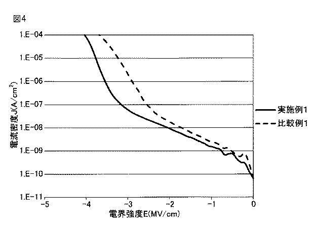
図1に実施例1及び比較例1のGI−SAX測定結果を示し、図2にGI−SAXS測定結果における散乱ベクトル(q)が0.05nm-1から0.25nm-1の範囲での拡大図を示す。図3に、実施例1のGI−SAXS測定結果と剛体球モデルで粒子体積割合13%とした時のフィッティング結果とを示す。また図4に実施例1及び比較例1のIV特性の測定結果を示す。 FIG. 1 shows the GI-SAX measurement results of Example 1 and Comparative Example 1, and FIG. 2 shows an enlargement of the scattering vector (q) in the GI-SAXS measurement result in the range of 0.05 nm −1 to 0.25 nm −1. The figure is shown. FIG. 3 shows the GI-SAXS measurement results of Example 1 and the fitting results when the particle volume ratio is 13% in the hard sphere model. FIG. 4 shows the measurement results of the IV characteristics of Example 1 and Comparative Example 1.
本発明の絶縁材料は、液晶表示素子、集積回路素子、半導体記憶素子、及び、固体撮像素子等の半導体装置用の層間絶縁膜、素子分離膜、STI用絶縁膜、PMD(Pre Metal Dielectric)膜、平坦化膜、表面保護膜、及び封止膜等として好適に使用できる。 The insulating material of the present invention includes an interlayer insulating film, an element isolation film, an STI insulating film, and a PMD (Pre Metal Dielectric) film for semiconductor devices such as liquid crystal display elements, integrated circuit elements, semiconductor memory elements, and solid-state imaging elements. , And can be suitably used as a planarizing film, a surface protective film, a sealing film, and the like.
Claims (4)
シリカ粒子を、13%以上20%以下である体積割合で含み、
炭素原子の珪素原子に対する組成比(C/Si)が0.54以上0.62以下であり、かつ
微小角入射X線小角散乱(GI−SAXS)測定における、散乱ベクトルqが0.1nm-1の時の散乱強度I1(q)の、該散乱ベクトルqが0.2nm-1の時の散乱強度I2(q)に対する比(I1(q)/I2(q))が、0.90以下である、半導体用絶縁材料。 A semiconductor insulating material containing silicon atoms, carbon atoms, and oxygen atoms,
Including silica particles in a volume ratio of 13 % or more and 20 % or less,
The composition ratio (C / Si) of carbon atoms to silicon atoms is 0.54 or more and 0.62 or less, and the scattering vector q is 0.1 nm −1 in small angle incident X-ray small angle scattering (GI-SAXS) measurement. The ratio (I 1 (q) / I 2 (q)) of the scattering intensity I 1 (q) at the time to the scattering intensity I 2 (q) when the scattering vector q is 0.2 nm −1 is 0 An insulating material for a semiconductor, which is 90 or less.
ポリシロキサン化合物及びシリカ粒子を含む材料組成物を基板に塗布し、前記材料組成物を焼成硬化させる工程を含み、
前記ポリシロキサン化合物は、下記一般式(1):
R1Si(OR2)3 (1)
(式中、R1は炭素数1〜10の炭化水素基であり、そしてR2は各々独立に炭素数1〜6の炭化水素基である。)
で表される1種以上のシランモノマー及び下記一般式(2):
Si(OR3)4 (2)
(式中、R3は各々独立に炭素数1〜6の炭化水素基である。)
で表される1種以上のシランモノマーを合計で50質量%以上の量で含むシラン成分を加水分解重縮合することで得られる、半導体用絶縁材料の製造方法。 A method for producing a semiconductor insulating material according to claim 1 or 2 ,
Applying a material composition containing a polysiloxane compound and silica particles to a substrate, and baking and curing the material composition;
The polysiloxane compound has the following general formula (1):
R 1 Si (OR 2 ) 3 (1)
(Wherein R 1 is a hydrocarbon group having 1 to 10 carbon atoms, and R 2 is each independently a hydrocarbon group having 1 to 6 carbon atoms.)
One or more silane monomers represented by the following general formula (2):
Si (OR 3 ) 4 (2)
(In the formula, each R 3 is independently a hydrocarbon group having 1 to 6 carbon atoms.)
The manufacturing method of the insulating material for semiconductors obtained by carrying out hydrolysis polycondensation of the silane component which contains the 1 or more types of silane monomer represented by these in the quantity of 50 mass% or more in total.
Priority Applications (1)
| Application Number | Priority Date | Filing Date | Title |
|---|---|---|---|
| JP2012211345A JP6042151B2 (en) | 2012-09-25 | 2012-09-25 | Insulating material for semiconductor containing silica particles |
Applications Claiming Priority (1)
| Application Number | Priority Date | Filing Date | Title |
|---|---|---|---|
| JP2012211345A JP6042151B2 (en) | 2012-09-25 | 2012-09-25 | Insulating material for semiconductor containing silica particles |
Publications (2)
| Publication Number | Publication Date |
|---|---|
| JP2014067829A JP2014067829A (en) | 2014-04-17 |
| JP6042151B2 true JP6042151B2 (en) | 2016-12-14 |
Family
ID=50743947
Family Applications (1)
| Application Number | Title | Priority Date | Filing Date |
|---|---|---|---|
| JP2012211345A Active JP6042151B2 (en) | 2012-09-25 | 2012-09-25 | Insulating material for semiconductor containing silica particles |
Country Status (1)
| Country | Link |
|---|---|
| JP (1) | JP6042151B2 (en) |
Families Citing this family (2)
| Publication number | Priority date | Publication date | Assignee | Title |
|---|---|---|---|---|
| JP6702325B2 (en) | 2015-08-05 | 2020-06-03 | 東亞合成株式会社 | Carbon analysis method |
| JP6476347B2 (en) | 2016-03-09 | 2019-02-27 | エルジー・ケム・リミテッド | Antireflection film |
Family Cites Families (8)
| Publication number | Priority date | Publication date | Assignee | Title |
|---|---|---|---|---|
| JP2006045352A (en) * | 2004-08-04 | 2006-02-16 | Hitachi Chem Co Ltd | Silica film-forming composition, silica film, its forming method and electronic part having silica film |
| JP5532550B2 (en) * | 2008-05-29 | 2014-06-25 | パナソニック株式会社 | Silicon compounds for dielectric films of plasma displays |
| JP5552791B2 (en) * | 2009-10-15 | 2014-07-16 | 住友ベークライト株式会社 | Method for producing transparent composite sheet and transparent composite sheet |
| JP5861995B2 (en) * | 2010-07-05 | 2016-02-16 | 住友ベークライト株式会社 | Resin composition, prepreg, resin layer, circuit board, and semiconductor device |
| JPWO2012086656A1 (en) * | 2010-12-20 | 2014-05-22 | 旭硝子株式会社 | Resin substrate having hard coat film and method for producing resin substrate having hard coat film |
| JP2012134302A (en) * | 2010-12-21 | 2012-07-12 | Jsr Corp | Method of filling trench, and composition for filling trench |
| JP2012136559A (en) * | 2010-12-24 | 2012-07-19 | Asahi Kasei E-Materials Corp | Method for producing polysiloxane condensation reaction product varnish |
| CN103283015A (en) * | 2010-12-24 | 2013-09-04 | 旭化成电子材料株式会社 | Insulation structure and method for manufacturing same |
-
2012
- 2012-09-25 JP JP2012211345A patent/JP6042151B2/en active Active
Also Published As
| Publication number | Publication date |
|---|---|
| JP2014067829A (en) | 2014-04-17 |
Similar Documents
| Publication | Publication Date | Title |
|---|---|---|
| JP5030478B2 (en) | Precursor composition of porous film and preparation method thereof, porous film and preparation method thereof, and semiconductor device | |
| US8603588B2 (en) | Composition and method for production thereof, porous material and method for production thereof, interlayer insulating film, semiconductor material, semiconductor device, and low-refractive-index surface protection film | |
| KR100956046B1 (en) | Precursor composition for porous membrane and process for preparation thereof, porous membrane and process for production thereof, and semiconductor device | |
| WO2010150861A1 (en) | Product of polysiloxane condensation | |
| JP5700615B2 (en) | Polysilazane-based trench filling composition | |
| JP5341944B2 (en) | Method of forming insulating film for trench filling using polysiloxane condensation reaction product | |
| JP2010153655A (en) | Polysiloxane-based reactant for filling trench | |
| JP6042151B2 (en) | Insulating material for semiconductor containing silica particles | |
| JP2012136559A (en) | Method for producing polysiloxane condensation reaction product varnish | |
| JP2012131864A (en) | Coating liquid for forming silica-based insulating film | |
| JP5826012B2 (en) | Insulating material containing polysiloxane condensate and method for producing cured film using the insulating material | |
| JP2004307693A (en) | Composition for forming porous film, method for producing porous film, porous film, interlayer dielectric film and semiconductor device | |
| JP6035098B2 (en) | Trench filling solution | |
| JP5878383B2 (en) | Polysiloxane material | |
| JP6077761B2 (en) | Polysiloxane composition | |
| JP5732121B2 (en) | Condensation reaction product for filling polysiloxane trench and method for producing trench filling film | |
| JP6016558B2 (en) | Method for producing silica-based coating | |
| JP2012131859A (en) | Coating liquid for formation of silica-based insulating film | |
| TW200403764A (en) | Low metal porous silica dielectric for integral circuit applications |
Legal Events
| Date | Code | Title | Description |
|---|---|---|---|
| A621 | Written request for application examination |
Free format text: JAPANESE INTERMEDIATE CODE: A621 Effective date: 20150625 |
|
| A977 | Report on retrieval |
Free format text: JAPANESE INTERMEDIATE CODE: A971007 Effective date: 20160303 |
|
| A131 | Notification of reasons for refusal |
Free format text: JAPANESE INTERMEDIATE CODE: A131 Effective date: 20160329 |
|
| A711 | Notification of change in applicant |
Free format text: JAPANESE INTERMEDIATE CODE: A712 Effective date: 20160404 |
|
| A521 | Written amendment |
Free format text: JAPANESE INTERMEDIATE CODE: A523 Effective date: 20160512 |
|
| TRDD | Decision of grant or rejection written | ||
| A01 | Written decision to grant a patent or to grant a registration (utility model) |
Free format text: JAPANESE INTERMEDIATE CODE: A01 Effective date: 20161101 |
|
| A61 | First payment of annual fees (during grant procedure) |
Free format text: JAPANESE INTERMEDIATE CODE: A61 Effective date: 20161109 |
|
| R150 | Certificate of patent or registration of utility model |
Ref document number: 6042151 Country of ref document: JP Free format text: JAPANESE INTERMEDIATE CODE: R150 |
|
| S531 | Written request for registration of change of domicile |
Free format text: JAPANESE INTERMEDIATE CODE: R313531 |
|
| R350 | Written notification of registration of transfer |
Free format text: JAPANESE INTERMEDIATE CODE: R350 |