JP6041304B2 - Illumination optical system for EUV microlithography, EUV attenuator for this type of illumination optical system, and illumination system and projection exposure apparatus having this type of illumination optical system - Google Patents
Illumination optical system for EUV microlithography, EUV attenuator for this type of illumination optical system, and illumination system and projection exposure apparatus having this type of illumination optical system Download PDFInfo
- Publication number
- JP6041304B2 JP6041304B2 JP2012501137A JP2012501137A JP6041304B2 JP 6041304 B2 JP6041304 B2 JP 6041304B2 JP 2012501137 A JP2012501137 A JP 2012501137A JP 2012501137 A JP2012501137 A JP 2012501137A JP 6041304 B2 JP6041304 B2 JP 6041304B2
- Authority
- JP
- Japan
- Prior art keywords
- attenuator
- euv
- illumination
- optical system
- facet
- Prior art date
- Legal status (The legal status is an assumption and is not a legal conclusion. Google has not performed a legal analysis and makes no representation as to the accuracy of the status listed.)
- Active
Links
- 238000005286 illumination Methods 0.000 title claims description 220
- 230000003287 optical effect Effects 0.000 title claims description 49
- 238000001393 microlithography Methods 0.000 title claims description 6
- 230000005855 radiation Effects 0.000 claims description 43
- 230000000295 complement effect Effects 0.000 claims description 10
- 238000009713 electroplating Methods 0.000 claims description 10
- 239000011248 coating agent Substances 0.000 claims description 9
- 238000000576 coating method Methods 0.000 claims description 9
- PXHVJJICTQNCMI-UHFFFAOYSA-N Nickel Chemical compound [Ni] PXHVJJICTQNCMI-UHFFFAOYSA-N 0.000 claims description 6
- 238000004519 manufacturing process Methods 0.000 claims description 5
- 230000003014 reinforcing effect Effects 0.000 claims description 4
- 229910052759 nickel Inorganic materials 0.000 claims description 3
- 238000000034 method Methods 0.000 claims description 2
- 210000001747 pupil Anatomy 0.000 description 44
- 238000012937 correction Methods 0.000 description 42
- 238000013461 design Methods 0.000 description 19
- 238000009826 distribution Methods 0.000 description 16
- 230000008901 benefit Effects 0.000 description 7
- 230000015572 biosynthetic process Effects 0.000 description 6
- 230000036961 partial effect Effects 0.000 description 6
- 230000002787 reinforcement Effects 0.000 description 5
- 230000009471 action Effects 0.000 description 4
- 230000002238 attenuated effect Effects 0.000 description 4
- 238000010521 absorption reaction Methods 0.000 description 3
- 230000005540 biological transmission Effects 0.000 description 3
- 238000013507 mapping Methods 0.000 description 3
- 239000000463 material Substances 0.000 description 3
- 238000005259 measurement Methods 0.000 description 3
- 238000007493 shaping process Methods 0.000 description 3
- 230000008859 change Effects 0.000 description 2
- 238000010586 diagram Methods 0.000 description 2
- 230000000694 effects Effects 0.000 description 2
- 230000003628 erosive effect Effects 0.000 description 2
- 238000002310 reflectometry Methods 0.000 description 2
- ZOKXTWBITQBERF-UHFFFAOYSA-N Molybdenum Chemical compound [Mo] ZOKXTWBITQBERF-UHFFFAOYSA-N 0.000 description 1
- XUIMIQQOPSSXEZ-UHFFFAOYSA-N Silicon Chemical compound [Si] XUIMIQQOPSSXEZ-UHFFFAOYSA-N 0.000 description 1
- 239000006096 absorbing agent Substances 0.000 description 1
- 229910052782 aluminium Inorganic materials 0.000 description 1
- XAGFODPZIPBFFR-UHFFFAOYSA-N aluminium Chemical compound [Al] XAGFODPZIPBFFR-UHFFFAOYSA-N 0.000 description 1
- 238000003491 array Methods 0.000 description 1
- 239000004020 conductor Substances 0.000 description 1
- 238000013016 damping Methods 0.000 description 1
- 238000000354 decomposition reaction Methods 0.000 description 1
- 230000007423 decrease Effects 0.000 description 1
- 230000004907 flux Effects 0.000 description 1
- 230000006872 improvement Effects 0.000 description 1
- 229910052751 metal Inorganic materials 0.000 description 1
- 239000002184 metal Substances 0.000 description 1
- 230000004048 modification Effects 0.000 description 1
- 238000012986 modification Methods 0.000 description 1
- 229910052750 molybdenum Inorganic materials 0.000 description 1
- 239000011733 molybdenum Substances 0.000 description 1
- 239000002086 nanomaterial Substances 0.000 description 1
- 238000005192 partition Methods 0.000 description 1
- 238000009304 pastoral farming Methods 0.000 description 1
- 238000001259 photo etching Methods 0.000 description 1
- 229920002120 photoresistant polymer Polymers 0.000 description 1
- 238000007747 plating Methods 0.000 description 1
- 238000012545 processing Methods 0.000 description 1
- 238000012887 quadratic function Methods 0.000 description 1
- 230000002829 reductive effect Effects 0.000 description 1
- 230000002441 reversible effect Effects 0.000 description 1
- 238000000926 separation method Methods 0.000 description 1
- 229910052710 silicon Inorganic materials 0.000 description 1
- 239000010703 silicon Substances 0.000 description 1
- 230000007704 transition Effects 0.000 description 1
Images


Classifications
-
- G—PHYSICS
- G03—PHOTOGRAPHY; CINEMATOGRAPHY; ANALOGOUS TECHNIQUES USING WAVES OTHER THAN OPTICAL WAVES; ELECTROGRAPHY; HOLOGRAPHY
- G03F—PHOTOMECHANICAL PRODUCTION OF TEXTURED OR PATTERNED SURFACES, e.g. FOR PRINTING, FOR PROCESSING OF SEMICONDUCTOR DEVICES; MATERIALS THEREFOR; ORIGINALS THEREFOR; APPARATUS SPECIALLY ADAPTED THEREFOR
- G03F7/00—Photomechanical, e.g. photolithographic, production of textured or patterned surfaces, e.g. printing surfaces; Materials therefor, e.g. comprising photoresists; Apparatus specially adapted therefor
- G03F7/70—Microphotolithographic exposure; Apparatus therefor
- G03F7/70058—Mask illumination systems
- G03F7/702—Reflective illumination, i.e. reflective optical elements other than folding mirrors, e.g. extreme ultraviolet [EUV] illumination systems
-
- G—PHYSICS
- G03—PHOTOGRAPHY; CINEMATOGRAPHY; ANALOGOUS TECHNIQUES USING WAVES OTHER THAN OPTICAL WAVES; ELECTROGRAPHY; HOLOGRAPHY
- G03F—PHOTOMECHANICAL PRODUCTION OF TEXTURED OR PATTERNED SURFACES, e.g. FOR PRINTING, FOR PROCESSING OF SEMICONDUCTOR DEVICES; MATERIALS THEREFOR; ORIGINALS THEREFOR; APPARATUS SPECIALLY ADAPTED THEREFOR
- G03F7/00—Photomechanical, e.g. photolithographic, production of textured or patterned surfaces, e.g. printing surfaces; Materials therefor, e.g. comprising photoresists; Apparatus specially adapted therefor
- G03F7/70—Microphotolithographic exposure; Apparatus therefor
- G03F7/70058—Mask illumination systems
- G03F7/70083—Non-homogeneous intensity distribution in the mask plane
-
- G—PHYSICS
- G03—PHOTOGRAPHY; CINEMATOGRAPHY; ANALOGOUS TECHNIQUES USING WAVES OTHER THAN OPTICAL WAVES; ELECTROGRAPHY; HOLOGRAPHY
- G03F—PHOTOMECHANICAL PRODUCTION OF TEXTURED OR PATTERNED SURFACES, e.g. FOR PRINTING, FOR PROCESSING OF SEMICONDUCTOR DEVICES; MATERIALS THEREFOR; ORIGINALS THEREFOR; APPARATUS SPECIALLY ADAPTED THEREFOR
- G03F7/00—Photomechanical, e.g. photolithographic, production of textured or patterned surfaces, e.g. printing surfaces; Materials therefor, e.g. comprising photoresists; Apparatus specially adapted therefor
- G03F7/70—Microphotolithographic exposure; Apparatus therefor
- G03F7/70058—Mask illumination systems
- G03F7/70091—Illumination settings, i.e. intensity distribution in the pupil plane or angular distribution in the field plane; On-axis or off-axis settings, e.g. annular, dipole or quadrupole settings; Partial coherence control, i.e. sigma or numerical aperture [NA]
- G03F7/701—Off-axis setting using an aperture
-
- G—PHYSICS
- G03—PHOTOGRAPHY; CINEMATOGRAPHY; ANALOGOUS TECHNIQUES USING WAVES OTHER THAN OPTICAL WAVES; ELECTROGRAPHY; HOLOGRAPHY
- G03F—PHOTOMECHANICAL PRODUCTION OF TEXTURED OR PATTERNED SURFACES, e.g. FOR PRINTING, FOR PROCESSING OF SEMICONDUCTOR DEVICES; MATERIALS THEREFOR; ORIGINALS THEREFOR; APPARATUS SPECIALLY ADAPTED THEREFOR
- G03F7/00—Photomechanical, e.g. photolithographic, production of textured or patterned surfaces, e.g. printing surfaces; Materials therefor, e.g. comprising photoresists; Apparatus specially adapted therefor
- G03F7/70—Microphotolithographic exposure; Apparatus therefor
- G03F7/70058—Mask illumination systems
- G03F7/70191—Optical correction elements, filters or phase plates for controlling intensity, wavelength, polarisation, phase or the like
Landscapes
- Physics & Mathematics (AREA)
- General Physics & Mathematics (AREA)
- Exposure And Positioning Against Photoresist Photosensitive Materials (AREA)
- Exposure Of Semiconductors, Excluding Electron Or Ion Beam Exposure (AREA)
- Optical Elements Other Than Lenses (AREA)
- Mounting And Adjusting Of Optical Elements (AREA)
- Microscoopes, Condenser (AREA)
Description
本発明は、照明光ビームを放射線源から物体視野に誘導するためのEUVマイクロリソグラフィのために、照明光ビームを誘導するための非平面ミラー表面形状を有する反射面を有する少なくとも1つのEUVミラーを有する照明光学系に関する。更に、本発明は、この種の照明光学系のためのEUV減衰器、この種の照明光学系を有する照明系、及びこの種の照明系を有する投影露光装置に関する。最後に、本発明は、微細構造化構成要素又はナノ構造化構成要素を生成する方法、及び本方法を用いて製造される構成要素に関する。 The present invention provides at least one EUV mirror having a reflective surface having a non-planar mirror surface shape for directing an illumination light beam for EUV microlithography for directing the illumination light beam from a radiation source to an object field. It has an illumination optical system. Furthermore, the present invention relates to an EUV attenuator for this type of illumination optical system, an illumination system having this type of illumination optical system, and a projection exposure apparatus having this type of illumination system. Finally, the present invention relates to a method for producing a microstructured component or a nanostructured component, and a component manufactured using the method.
投影露光装置における照明光学系のための減衰器は、US 2007/0041004 A1、US 6,445,510 B1、及びUS 2007/0058274 A1から公知である。 Attenuators for illumination optics in a projection exposure apparatus are known from US 2007/0041004 A1, US 6,445,510 B1 and US 2007/0058274 A1.
本発明の目的は、可能な限り少ない望ましくない放射線損失しか伴わずに物体視野にわたる照明パラメータ、例えば、照明強度分布又は照明角度分布における望ましくない変化を補正することができるような冒頭に示した種類の照明光学系を開発することである。 The object of the present invention is the kind indicated at the outset so that it is possible to correct undesired changes in the illumination parameters, for example the illumination intensity distribution or the illumination angle distribution, over the object field with as little unwanted radiation loss as possible. Is to develop an illumination optical system.
本発明は、照明光ビームを形成するための非平面ミラー表面形状を有する反射面を有する少なくとも1つのEUVミラーと、EUVミラーの前に配置された少なくとも1つのEUV減衰器であって、EUV減衰器のEUVミラーの反射面に対面する減衰器面が、ミラー表面形状を補完するように設計された減衰器表面形状を有し、それによって減衰器面のうちの少なくともある区画が、反射面に接触することなく反射面から一定の間隔の位置に配置されるようにするEUV減衰器とを有して、照明光ビームを放射線源から物体視野に誘導するためのEUVマイクロリソグラフィのための照明光学系によってこの目的を達成する。 The present invention relates to at least one EUV mirror having a reflective surface having a non-planar mirror surface shape for forming an illumination light beam, and at least one EUV attenuator disposed in front of the EUV mirror, comprising: attenuator surface facing the reflective surface of the EUV mirrors vessel has an attenuator surface shape designed to complement the mirror surface shape, whereby at least one partition of the attenuator surface, the reflective surface Illumination optics for EUV microlithography for directing an illumination light beam from a radiation source to an object field with an EUV attenuator arranged to be spaced from the reflecting surface without contact The system achieves this goal.
本発明に準ずると、照明パラメータにおける望ましくない変化が、EUV減衰器を用いて補正される。ミラー表面形状に対する減衰器表面形状の補完的成形は、EUV減衰器をEUVミラーの直近に持ってくることができることを保証する。照明光ビームがEUVミラーに0とはかなり異なる入射角で当たった場合であっても、EUV減衰器をEUVミラーの直近に持ってくるこの可能性は、EUV減衰器上への照明光の戻りビームの入射位置と射出ビームの入射位置の間のオフセットに起因する二重通過損失が阻止されるか、又は最小にされることを保証する。EUVミラーとは別のサブアセンブリの形態にあるEUV減衰器の利点は維持される。従って、EUV減衰器をEUVミラーに対して微調節することができる。更に、照明パラメータの影響を変更するために、特定のEUV減衰器を異なる設計のEUV減衰器と交換することができる。非常に短い間隔にも関わらず、EUVミラーとEUV減衰器とが互いに接触することを安全に阻止することができる。EUV減衰器は、物体視野にわたる照明光における照明角度分布と強度分布の両方に影響を与えるために使用することができる。EUV減衰器の作用は、照明光学系内のその位置に依存する。EUV減衰器のこの位置決めされのために設けられたEUVミラーの前の平面では、この平面の状況に従って物体視野照明の視野機能と瞳機能の両方に関するパラメータを変更することができる。EUV減衰器が、照明光学系の視野平面又は瞳平面と一致する平面に位置する限り、視野機能のパラメータのみ、又は瞳機能のパラメータだけに特定的に影響を与えることができる。非平面ミラー表面形状は、ミラー表面形状に対して補完的な設計の減衰器表面形状も同じく非平坦、すなわち、不均等であることを意味する。非平坦ミラー表面形状は、ミラーの反射面内の対応する曲率により、又はそうでなければミラーが個々のミラーセグメント、例えば、個々のミラーファセットに分割されることによって生成することができる。 In accordance with the present invention, undesirable changes in illumination parameters are corrected using an EUV attenuator. Complementary shaping of the attenuator surface shape for the mirror surface shape ensures that it is possible to bring the EUV attenuator nearest EUV mirror. This possibility of bringing an EUV attenuator in the immediate vicinity of the EUV mirror, even when the illumination light beam hits the EUV mirror at an angle of incidence significantly different from 0, is the return of the illumination light onto the EUV attenuator. It is ensured that the double pass loss due to the offset between the incident position of the beam and the incident position of the exit beam is prevented or minimized. The advantage of an EUV attenuator in the form of a subassembly separate from the EUV mirror is maintained. Therefore, the EUV attenuator can be fine-tuned with respect to the EUV mirror. Furthermore, certain EUV attenuators can be replaced with different designs of EUV attenuators in order to change the influence of the illumination parameters. Despite the very short distance, it is possible to safely prevent the EUV mirror and EUV attenuator from contacting each other. An EUV attenuator can be used to affect both the illumination angle distribution and the intensity distribution in the illumination light over the object field. The action of the EUV attenuator depends on its position in the illumination optics. In the plane in front of the EUV mirror provided for this positioning of the EUV attenuator, the parameters for both the field function and the pupil function of the object field illumination can be changed according to the situation of this plane. As long as the EUV attenuator is located in a plane that coincides with the field plane or pupil plane of the illumination optics, it can specifically affect only the field function parameters or only the pupil function parameters. Non-planar mirror surface shape, the attenuator surface shape of complementary design to the mirror surface shape similarly textured, i.e., it means that unequal. A non-flat mirror surface shape can be generated by a corresponding curvature in the reflective surface of the mirror, or otherwise by dividing the mirror into individual mirror segments, eg, individual mirror facets.
EUV減衰器とEUVミラーの間の200μmよりも大きくない領域内の間隔は特に適切であることが見出されている。 A spacing in the region not larger than 200 μm between the EUV attenuator and the EUV mirror has been found to be particularly suitable.
EUV減衰器は、規定の絞り輪郭を有する少なくとも1つのEUV絞りを有することができる。それによってEUV減衰器からの明確に定められた減衰作用を保証する。いかなる減衰も必要とされない点では、照明光は、完全にEUV減衰器を通過することが許され、又はEUV減衰器によって通過することが許されて減衰されない。 The EUV attenuator can have at least one EUV stop with a defined stop profile. This ensures a well-defined attenuation effect from the EUV attenuator. In that no attenuation is required, the illumination light is allowed to pass completely through the EUV attenuator or is allowed to pass by the EUV attenuator and is not attenuated.
代替的又は追加的に、EUV減衰器は、少なくとも1つの灰色フィルタ、すなわち、灰色フィルタ機能を有する構成要素を有することができる。これは、灰色フィルタによるEUV減衰作用のプロフィールの適切に精密な成形により、EUV減衰器からの減衰作用プロフィールの精密な成形を可能にする。これは、照明光の強度を補正関数に準じて変調することができることを意味する。物体視野照明における楕円度又はそうでなければテレセントリック性の程度を変調するか又はこれらに影響を与えるために、物体視野の照明の均一性の程度、すなわち、均一性の程度に影響を与えるか、又はこれらを変調することができる。また、物体視野照明における極均衡として公知の定義方式で規定された照明角度からの照明強度の間の強度比を変調するか又はそれに影響を与えることができる。言及したこれらのパラメータのうちの単一のもの又はそうでなければ全てを変調するか又はこれらに影響を与えることができる。 Alternatively or additionally, the EUV attenuator can have at least one gray filter, i.e. a component having a gray filter function. This allows for precise shaping of the attenuation action profile from the EUV attenuator by appropriately precise shaping of the EUV attenuation action profile with the gray filter. This means that the intensity of illumination light can be modulated according to the correction function. Influence the degree of uniformity of the object field illumination, i.e. the degree of uniformity, in order to modulate or influence the degree of ellipticity or otherwise telecentricity in the object field illumination; Or they can be modulated. It is also possible to modulate or influence the intensity ratio between the illumination intensities from the illumination angles defined in a well-known definition as pole balance in object field illumination. Any one or all of these mentioned parameters can be modulated or influenced.
EUVミラーの反射面は、自由曲面の形態にあるとすることができる。それによって物体視野照明を特定の事前設定に適合させることが可能になる。必要に応じて、自由曲面設計のものであるEUVミラーにより、例えば、矩形物体視野を照明することができる。 The reflective surface of the EUV mirror can be in the form of a free-form surface. This makes it possible to adapt the object field illumination to specific presets. If necessary, for example, a rectangular object field can be illuminated by an EUV mirror having a free-form surface design.
EUVミラーの反射面は、複数の反射個別ファセットを有するファセット面の形態にあるとすることができ、少なくとも一部の特定の個別ファセットは、EUV減衰器の関連付けられた減衰器区画を有することができる。この種の減衰器区画は、複数の個別ファセットに関連付けることができる。この設計のファセットミラーは、特に、例えば、US 2007/0058274 A1の図12から公知である照明幾何学形状の視野ファセットミラー又は瞳ファセットミラーとすることができる。この種のファセットミラーのファセットは、特に個別に傾けるか、又は傾斜させることができる。この場合、個別ファセットは、EUVミラーの主平面に対して、0.5°よりも大きく、1°よりも大きく、2°よりも大きく、3°よりも大きく、又は5°よりも大きい傾斜角だけ個別に傾斜させることができる。更に、ファセットは、ビームを形成するために曲面の特に凹曲面の反射面を有することができる。そのような設計は、特に物体視野照明パラメータに影響を与えるために、EUV減衰器を用いて特定の個別ファセットを減衰させることを可能にする。個別減衰器区画及び/又は複数のそのような減衰器区画を含む組合せを特にモノリシックに形成された本体から製造することができる。これは電気メッキによって形成された本体とすることができる。 The reflective surface of the EUV mirror can be in the form of a faceted surface having a plurality of reflective individual facets, and at least some particular individual facets can have an associated attenuator section of the EUV attenuator. it can. This type of attenuator section can be associated with multiple individual facets. The facet mirror of this design can in particular be a field facet mirror or a pupil facet mirror with illumination geometry as known from FIG. 12 of US 2007/0058274 A1, for example. The facets of this type of facet mirror can in particular be tilted individually or tilted. In this case, the individual facets are inclined with respect to the main plane of the EUV mirror greater than 0.5 °, greater than 1 °, greater than 2 °, greater than 3 °, or greater than 5 °. Can only be individually tilted. Furthermore, the facets can have a curved reflective surface, in particular a concave curved surface, to form a beam. Such a design makes it possible to attenuate specific individual facets using an EUV attenuator, in particular in order to influence the object field illumination parameters. Combinations comprising individual attenuator sections and / or a plurality of such attenuator sections can be produced in particular from a monolithically formed body. This can be a body formed by electroplating.
減衰器区画は、個別減衰をもたらすことができる。例示的に、各々が異なる減衰を有する2つの種類の減衰器区画、又はそうでなければ2つよりも多くの種類の減衰器区画、例えば、3つ、4つ、5つ、又は更にはそれ以上のそのような種類を設けることができる。それによって相応に大きい自由度数で物体視野照明パラメータに影響を与えることが可能になる。 The attenuator section can provide individual attenuation. Illustratively, two types of attenuator compartments each having a different attenuation, or otherwise more than two types of attenuator compartments, eg, three, four, five, or even more Such types can be provided. This makes it possible to influence the object field illumination parameters with a correspondingly large degree of freedom.
減衰器区画は、個別ファセットに関連付けられた遮蔽縁部を有する絞りの形態にあるとすることができる。それによって個別ファセットを個別化方式で精密に減衰させることが可能になる。 The attenuator section may be in the form of a diaphragm having a shielding edge associated with an individual facet. As a result, individual facets can be attenuated precisely in an individualized manner.
ファセット面は、複数のファセットブロックに分割することができる。更に、ファセットブロックは、複数の個別ファセットを組み合わせることができる。ファセットブロックは、ファセット面上に挿入された距離区画を有することができる。EUV減衰器の補完的に成形された減衰器面は、ファセット面上の距離区画に隣接して配置された減衰器面区画上に補強支柱を有することができる。それによってEUV減衰器を自己支持設計のものとすることが可能になり、補強支柱がない場合には、有用放射線の望ましくない有意な損失がもたらされる。 The facet surface can be divided into a plurality of facet blocks. Furthermore, a facet block can combine multiple individual facets. The facet block can have a distance section inserted on the facet surface. The complementary shaped attenuator surface of the EUV attenuator can have reinforcing posts on the attenuator surface section located adjacent to the distance section on the facet surface. This allows the EUV attenuator to be of a self-supporting design, and in the absence of reinforcing struts results in undesirable significant loss of useful radiation.
EUV減衰器の補完的に成形された減衰器面は、特に電気メッキによってEUVミラーの反射面から形成された層の形態にあるとすることができる。それによって減衰器面においてEUVミラーの反射面に対する精密な補完形状を保証する。更に、それによって2つの面を互いから非常に短い間隔で配置する可能性がもたらされる。 The complementary shaped attenuator surface of the EUV attenuator can be in the form of a layer formed from the reflective surface of the EUV mirror, in particular by electroplating. This ensures a precise complementary shape to the reflective surface of the EUV mirror at the attenuator surface. Furthermore, it offers the possibility to place the two surfaces at a very short distance from each other.
EUV減衰器の形成層は、ニッケルから生成することができる。それによって精密な形成に加えて、EUV減衰器を小さい壁厚を有するように設計することも可能になり、更にそれによって特に二重通過における有用放射線の望ましくない損失が低減する。EUV減衰器における壁厚は、0.03mmよりも大きく、又はそれに等しいとすることができる。壁厚は、0.03mmと0.3mmの間の範囲、特に0.05mmと0.3mmの間の範囲にあるとすることができる。 The formation layer of the EUV attenuator can be made from nickel. In addition to precise formation, it also makes it possible to design the EUV attenuator with a small wall thickness, which further reduces the undesirable loss of useful radiation, especially in the double pass. The wall thickness in the EUV attenuator can be greater than or equal to 0.03 mm. The wall thickness can be in the range between 0.03 mm and 0.3 mm, in particular in the range between 0.05 mm and 0.3 mm.
形成層は、複数の絞りを収容することができる。それによって特にEUVミラーの領域、特にファセットミラーの形態にあるEUVミラーの個別ファセットの個別化遮蔽が可能になる。 The forming layer can accommodate a plurality of stops. This allows individualized shielding of the individual facets of the EUV mirror, in particular in the region of the EUV mirror, in particular in the form of a facet mirror.
減衰器区画に加えて、形成層は、非減衰貫通開口部を収容することができる。この場合、EUVミラーは、物体視野照明パラメータに影響を与えるために減衰を必要とする点においてのみ減衰される。EUVミラーのファセット設計には、EUV減衰器の減衰器区画による影響を受ける照明を有する補正ファセットのみならず、EUV減衰器内に関連付けられた非減衰貫通開口部を有する影響を受けない基本照明ファセットを設けることができる。 In addition to the attenuator compartment, the forming layer can accommodate a non-attenuating through opening. In this case, the EUV mirror is attenuated only at points that require attenuation to affect the object field illumination parameters. The EUV mirror facet design includes not only a correction facet with illumination affected by the attenuator section of the EUV attenuator, but also an unaffected basic illumination facet with an unattenuated through aperture associated within the EUV attenuator. Can be provided.
EUV減衰器の減衰器区画が、関連付けられた一部の個別ファセットを有する限り、この減衰器区画は、絞りである複数の減衰器指状体を有することができる。この場合、各減衰器指状体は、この減衰器指状体が関連付けられる少なくとも1つの個別ファセットに対して個別に調整される方式で形成することができる。それによって照明光学系のためのEUV減衰器を製造する自由度が高まる。 As long as the attenuator section of the EUV attenuator has some individual facets associated with it, this attenuator section can have a plurality of attenuator fingers that are diaphragms. In this case, each attenuator finger can be formed in a manner that is individually adjusted with respect to at least one individual facet with which the attenuator finger is associated. This increases the degree of freedom for manufacturing EUV attenuators for illumination optics.
減衰器指状体の個別に成形された遮蔽縁部は、照明に対する適切な個別補正の任意選択肢をもたらす。 The individually shaped shielding edges of the attenuator fingers provide an option for proper individual correction for illumination.
各個別ファセットが、厳密に1つ又は最大で2つの関連付けられた減衰器指状体を有する関連付けは、EUV減衰器において小型で、同時に取り扱いの容易な設計を可能にする。 An association in which each individual facet has exactly one or at most two associated attenuator fingers allows a design that is compact and easy to handle at the same time in an EUV attenuator.
減衰器指状体は、共通の装着支持体によって保持することができる。それによって複数の個別ファセットに関連付けられる減衰器区画を共通の装着支持体と共にモジュールとして事前に組み立てる可能性がもたらされる。 The attenuator fingers can be held by a common mounting support. This provides the possibility of pre-assembling attenuator sections associated with a plurality of individual facets as a module with a common mounting support.
装着支持体は、複数の個別ファセットを有するファセットブロックの両側に配置された支持ブラケットを有することができ、減衰器指状体は、ファセットブロックに関連付けられた2つの支持ブラケットの間に配置される。それによって望ましくない遮蔽によってファセットミラーの可能な限り小さい有用反射面しか失われるこことのない減衰器指状体に対する装着支持体が可能になる。 The mounting support can have support brackets disposed on both sides of a facet block having a plurality of individual facets, and the attenuator fingers are disposed between two support brackets associated with the facet block. . This allows for a mounting support for the attenuator finger that is lost due to undesired shielding, where only the smallest possible reflective surface of the facet mirror is lost.
減衰器指状体に対する支持ブラケット上の保持点は、張られる個別ファセットの形状に依存するレベル、特にこれらの個別ファセットの反射面の外形に依存するレベルに配置することができる。このようにして、支持ブラケットの設計は、減衰器指状体と、それに関連付けられた個別ファセットの間の間隔を精密に規定することができる。 The holding points on the support brackets for the attenuator fingers can be arranged at a level that depends on the shape of the individual facets to be stretched, in particular at a level that depends on the contour of the reflective surface of these individual facets. In this way, the support bracket design can precisely define the spacing between the attenuator fingers and the associated individual facets.
本発明の照明光学系のためのEUV減衰器の利点、本発明の照明光学系を有する照明系の利点、及び本発明の照明系を有する投影露光装置の利点は、本発明の照明光学系を参照して上述したものに対応する。 The advantages of the EUV attenuator for the illumination optical system of the present invention, the advantage of the illumination system having the illumination optical system of the present invention, and the advantage of the projection exposure apparatus having the illumination system of the present invention are the advantages of the illumination optical system of the present invention. It corresponds to what has been described above with reference.
レチクルが準備される段階と、照明光に対して感光性を有するコーティングを有するウェーハが準備される段階と、本発明の投影露光装置を用いてレチクルの少なくとも1つの区画がウェーハ上に投影される段階と、照明光ビームに露光された感光層がウェーハ上で現像される段階とを含む製造方法の利点、及び本発明に準じて製造された微細構造又はナノ構造のサブアセンブリの利点は、本発明の照明光学系を参照して上述したものに対応する。 A step in which a reticle is prepared, a step in which a wafer having a coating that is sensitive to illumination light is provided, and at least one section of the reticle is projected onto the wafer using the projection exposure apparatus of the present invention. The advantages of the manufacturing method comprising the steps and a step in which the photosensitive layer exposed to the illumination light beam is developed on the wafer, and the advantages of the substructures of microstructures or nanostructures manufactured according to the present invention are as follows: This corresponds to that described above with reference to the illumination optics of the invention.
本発明の例示的な実施形態を図面を参照して以下により詳細に説明する。 Exemplary embodiments of the invention are described in more detail below with reference to the drawings.
図1は、マイクロリソグラフィのための投影露光装置1を通る子午断面を略示している。投影露光装置1における照明系2は、放射線源3だけではなく、物体平面6内の物体視野5を露光させるための照明光学系4を有する。この露光は、微細構造又はナノ構造の導体構成要素を生成するために物体視野5に配置され、投影露光装置1を用いて投影される構造を保持する図1には示していないレチクルの露光を含む。
FIG. 1 schematically shows a meridional section through a projection exposure apparatus 1 for microlithography. The illumination system 2 in the projection exposure apparatus 1 has an illumination optical system 4 for exposing not only the
投影光学系7は、物体視野5を像平面9内の像野8内にマップするのに使用される。レチクル上の構造は、像平面9内の像野8の領域に配置された図面には示していないウェーハのフォトレジスト層上にマップされる。
放射線源3は、5nmと30nmの間の範囲の有用放射線を放出するEUV放射線源である。この光源は、プラズマ光源、例えば、GDPP(ガス放電生成プラズマ)光源又はLPP(レーザ生成プラズマ)光源とすることができる。他のEUV放射線源、例えば、シンクロトロンに基づくものも可能である。
The
放射線源3から射出するEUV放射線10は、コレクター11によって集光される。適切なコレクターは、例えば、EP 1 225 481 Aから公知である。コレクター11の後に、EUV放射線10は中間焦点面12を通じて伝播し、その後に、視野ファセットミラー13に当たる。視野ファセットミラー13は、照明光学系4の物体平面6に対して光学的に共役な平面に配置される。
以降EUV放射線10を照明光又はマッピング光とも呼ぶ。
Hereinafter, the
視野ファセットミラー13の後に、EUV放射線10は、瞳ファセットミラー14によって反射される。瞳ファセットミラー14は、照明光学系4の投影光学系7の瞳平面に対して光学的に共役な平面に配置される。瞳ファセットミラー14と、EUV放射線10に対する光線経路の順に示しているミラー16、17、及び18を有する伝達光学系15の形態にあるマッピング光学アセンブリとは、視野ファセットミラー13の視野ファセット19(図2を参照されたい)を互いの上に重なるように物体視野5内にマップするのに使用される。伝達光学系15内の最後のミラー18はかすめ入射ミラーである。伝達光学系15を視野ファセットミラー13から物体視野5にEUV放射線10を伝達するための連続光学系とも呼ぶ。
After the
位置関係の説明を簡略化するために、下記の本文では直交xyz座標系を使用する。図1では、x軸は、作図面と垂直に閲覧者に向いて延びている。図1では、y軸は右に延びている。図1では、z軸は上方に延びている。 In order to simplify the description of the positional relationship, an orthogonal xyz coordinate system is used in the following text. In FIG. 1, the x-axis extends toward the viewer perpendicular to the drawing. In FIG. 1, the y-axis extends to the right. In FIG. 1, the z-axis extends upward.
図示していないレチクルホルダによって保持されるレチクルと、図示していないウェーハホルダによって保持されるウェーハとは、投影露光装置1の作動中にy方向に同期して走査される。 A reticle held by a reticle holder (not shown) and a wafer held by a wafer holder (not shown) are scanned in synchronization with the y direction during the operation of the projection exposure apparatus 1.
物体視野5は、弓形又は矩形の形状とすることができる。物体視野5のx広がりとy広がりとのアスペクト比は、視野ファセット19のアスペクト比に対応する。図示の例示的な実施形態では、視野ファセット19は矩形である。視野ファセット19は、図示していない実施形態では弓形とすることができ、そのような弓形視野ファセットのx方向の広がりとy方向の広がりとの比は、図示の実施形態における矩形視野ファセット19におけるアスペクト比に対応する。
The
視野ファセット19及び物体視野5のx/yアスペクト比は、例えば、13/1である。1よりも大きい他のアスペクト比も可能である。これらのアスペクト比に基づいて、x軸を長視野軸とも呼び、y軸を短視野軸とも呼ぶ。物体視野5内の特定のx座標を視野レベルとも呼ぶ。
The x / y aspect ratio of the
視野ファセットミラー13の視野ファセット19は、視野ファセットブロック20内でそれぞれの複数の視野ファセット19と組み合わされる。図2に示している視野ファセットミラー13の概略図では、図示の4つの視野ファセットブロック20の各は8つの視野ファセット19を有する。実際には、図4に示している更に別の実施形態の視野ファセットミラー13の図から分るように、非常に多数のそのような視野ファセットブロック20が存在する。実際には、視野ファセットミラー13は、数百の視野ファセット19を有する。視野ファセットブロック20は、実際には複数の自由度で調節することができる視野ファセット支持体21上に配置される。上部に視野ファセットブロック20が配置された視野ファセット支持体21は、視野ファセットミラー13における主平面を規定する。視野ファセット19の特定のもの又は視野ファセット19の全てが、視野ファセットミラー13の主平面に対して、例えば、0.5よりも大きい傾斜角だけ個別に傾斜される。視野ファセット19の特定のものでは、傾斜角は、1°よりも大きく、2°よりも大きく、3°よりも大きく、又はそうでなければ5°よりも大きいとすることができる。視野ファセットミラー13の主平面に対して5°よりも有意に大きい傾斜角も可能である。視野ファセットミラー13の設計に基づいて、視野ファセットブロック20を視野ファセット支持体21に対して調節可能な形状のものとすることができる。
The
瞳ファセットミラー14(図2を参照されたい)は、瞳ファセット支持体23上に、例えば、密充填六角形状で配置された複数の円形瞳ファセット22を有する。
The pupil facet mirror 14 (see FIG. 2) has a plurality of circular pupil facets 22 arranged on a
視野ファセット19と瞳ファセット22とはマッピング作用を有することができ、例えば、球形に凹の形状に成形することができる。
The
瞳ファセット支持体23は、視野ファセット支持体21に準じて調節することができるように設計することができる。瞳ファセット支持体23の調節可能性とは別に又はそれに追加して、個別瞳ファセット22を瞳ファセット支持体23に対して調節可能な設計のものとすることができる。
The
実際には、ファセット19、22上の高反射コーティングは、交替するモリブデン層とシリコン層とを有する多層コーティングである。この種の多層コーティングを製造するための他のコーティング材料も可能である。ファセット19、22は、EUV放射線10に対するミラーファセットである。個別視野ファセットブロック20及び/又は個別瞳ファセット22を調節するために、これらの構成要素をそれに関連付けられたアクチュエータに個別に接続さることができる。これらのアクチュエータは、個別視野ファセットブロック又は個別ファセットをそれぞれのファセットブロック又はそれぞれのファセットの反射平面に位置する2つの軸の回りに傾斜させることを可能にするような形態にあるとすることができる。
In practice, the highly reflective coating on
視野ファセット19は、各々個別に瞳ファセット22に関連付けられ、それによって視野ファセット19のうちのそれぞれの1つに当たるEUV放射線10の照明光ビームの成分が、関連付けられた瞳ファセット22を通じて物体視野5に転送されるようにする。従って、2つのファセットミラー13、14は、チャンネル毎にEUV放射線10を物体視野5に伝達する複数の照明チャンネルを定める。図2に略図示の実施形態は、合計で32個のそのような照明チャンネルを有する。放射線源3は、照明チャンネルの各々内の瞳ファセット22上にマップされる。
The
視野ファセット19及び瞳ファセット22は、2つのそれぞれのファセット型に分割される。図2は、基本照明視野ファセット19Gを模様なし形式で示している。図2は、補正照明視野ファセット19Kを陰付き形式で示している。基本照明視野ファセット19Gは、照明チャンネルを通じてこれらの視野ファセット19Gに関連付けられた基本照明瞳ファセット22Gを有し、この基本照明瞳ファセット22Gを模様なし円で示している。
The
補正照明視野ファセット19Kは、照明チャンネルを通じてこれらの補正照明視野ファセット19Kに関連付けられた補正照明瞳ファセット22Kを有し、この補正照明瞳ファセット22Kを陰付き円で示している。
The corrected
基本照明視野ファセット19Gは、関連付けられた基本照明瞳ファセット22Gを用いて基本照明チャンネルを通じて物体視野5の基本照明を与える。補正照明視野ファセット19Kは、関連付けられた補正照明瞳ファセット22Kを用いて基本照明チャンネルを通じて物体視野5の基本照明を与える。
The basic
視野ファセットミラー13の視野ファセット19のうちのどれが基本照明視野ファセット19Gとして使用されるかの選択、及び視野ファセット19のうちのどれが補正照明視野ファセット19Kとして使用されるかの選択は、EUV放射線10の照明光ビームによる視野ファセットミラー13の照明の幾何学形状及び強度分布、並びに物体視野5の規定の望ましい照明に従って行われる。例示的に、使用される補正照明視野ファセット19Kは、照明が基本照明には不十分な強度しか持たないもの又は照明が基本照明には許容不能である強度分布を有するものである。使用される補正照明視野ファセット19Kは、例えば、境界にある視野ファセット19、又は例えば遮蔽現象にある程度起因してEUV放射線が当たらないか、又はある程度減衰して当たる視野ファセット19とすることができる。
The selection of which of the
補正照明視野ファセット19Kは、規定の絞り輪郭を有するEUV絞りの形態にある関連付けられたEUV減衰器を有する。図3は、この種のEUV絞り24を有する補正照明視野ファセット19K1から19K6及び19K1'から19K6'を陰付き形式で絞り輪郭25と共に図示している。EUV絞り24は、補正照明ファセット19Kの反射面からのある間隔の位置に配置される。この間隔は最大で200μmであるが、他方では0よりも大きく、これは、EUV絞り24が、補正照明ファセット19Kに接触しないことを意味する。
The correction
各EUV絞り24は、関連付け補正照明視野ファセット19Kに対する減衰器区画として使用される。
Each
この場合、補正照明視野ファセット19K1から19K6は、補正照明視野ファセットブロック20K内で組み合わされる。補正照明視野ファセット19K1'から19K6'は、補正照明視野ファセットブロック20K'内で組み合わされる。これらの補正照明視野ファセット19K1から19K6及び19K1'から19K6'は、陰付き形式で示している区画においてEUV絞り24によって覆われ、それによってそこに入射するEUV放射線10が遮蔽される。この遮蔽は、EUV放射線10の吸収により、又は光線経路からのEUV放射線10の反射とそれに続く吸収とによって行うことができる。EUV絞り24の絞り輪郭25の形状は、補正照明視野ファセット19K1から19K6において各場合に異なる。補正照明視野ファセット19K1と19K1'とは、等しい形の絞り24を有する。それに従ってこれは、補正照明視野ファセットの対19K2/19K2'から19K6/19K6'に適用される。2つの視野ファセットブロック20Kと20K'とは、x/z鏡像対称平面に関して互いに対して鏡像対称で配置される。
In this case, the corrected
補正照明視野ファセット19K1から19K6における絞り24の絞り輪郭25の異なる設計に起因して、これらの補正照明視野ファセット19K1から19K6は、x方向に異なるそれぞれの分布でEUV放射線10を減衰させる。
Due to the different design of
補正照明視野ファセット19K1の絞り24は、図3の左手の境界でEUV放射線10を完全に減衰させる。減衰は、右手境界に向けて線形に減少し、従って、EUV放射線10は、右手の境界において可能な最大の効率で反射される。
The
補正照明視野ファセット19K2は、厳密に逆の減衰プロフィールをもたらす絞り輪郭25を有する関連付けられたEUV絞り24を有し、従って、このEUV絞り24は、図3の左手の境界においていかなる減衰ももたらされず、右手の境界においてEUV放射線10の最大減衰をもたらす。
The corrected
補正照明視野ファセット19K3は、図3の上部と下部から補正照明視野ファセット19K3の中心で接触する2つの三日月形区画を有する絞り輪郭25を有する絞り24を有する。従って、補正照明視野ファセット19K3は、x方向に図3の左手の境界における最小減衰で始まり、半分のxレベルにおける最大減衰に移行し、更に右手の境界における最小減衰に戻る減衰プロフィールを有する。
The corrected
補正照明視野ファセット19K4の絞り24は、補正照明視野ファセット19K3と比較してx方向にEUV放射線の逆減衰プロフィールを有する。補正照明視野ファセット19K3と19K4とは、x方向に放物線減衰プロフィールを生成する。
The
補正照明視野ファセット19K5の絞り24は、x方向に図3の左手の境界におけるEUV放射線10の最小減衰で始まり、右手の境界における最大減衰に戻る減衰プロフィールを有する。2つの境界の間では、減衰は、x座標への非線形依存性を有する。この場合、減衰は、穏やかな単調関数に従う。他の減衰機能プロフィール、特に少なくとも1つの最小値又は少なくとも1つの最大値を有するもの、更に、揺らぎ分布を有することも可能である。
The
補正照明視野ファセット19K6の絞り24は、x方向に補正照明視野ファセット19K5のものとは逆の減衰プロフィールを有する。
The
補正照明視野ファセット対19K1/19K1'から19K6/19K6'は、それぞれ、関連付けられたそれぞれのEUV絞り24に起因して長視野寸法にわたって、すなわち、x軸に沿って同じ反射率分布を有する標準化された補正照明視野ファセットの群を形成する。 The corrected illumination field facet pairs 19 K1 / 19 K1 ′ to 19 K6 / 19 K6 ′ each have the same reflectance distribution over the long field dimension, ie along the x-axis, due to the respective EUV stop 24 associated therewith. Form a group of standardized correction illumination field facets having
補正照明視野ファセットの対19K1/19K1'から19K6/19K6'は、それぞれ瞳ファセットミラー14の中心26に対して点対称に配置された、関連付けられた補正照明瞳ファセット対22K1/22K1'から22K6/22K6'を有する。
Corrected illumination field facet pairs 19 K1 / 19 K1 ′ through 19 K6 / 19 K6 ′ are each associated with an associated corrected illumination pupil facet pair 22 K1 / 22, which are arranged point-symmetrically with respect to the
それによって補正照明チャンネルによって物体視野照明のいかなるテレセントリック性変化ももたらされないことを保証する。 This ensures that the correction illumination channel does not result in any telecentricity change of the object field illumination.
テレセントリック性は、物体視野5の照明において以下の通りに定められる。
Telecentricity is determined in the illumination of the
照明物体視野5の全ての視野点に対して、この視野点に関連する光束における重心光線が定められる。この場合、重心光線は、この視野点から射出する光束のエネルギ重み付き方向を有する。理想的には、全ての視野点において、重心光線は、照明光学系又は投影光学系7によって規定される主光線と平行に進む。
For all field points of the illuminated
主光線の方向:
![]()

![]()
E(u,v,x,y)は、瞳座標u,vに基づく視野点x,yにおけるパワー分布であり、すなわち、この関連の視野点x,yにおける照明角に基づくパワー分布である。 E (u, v, x, y) is a power distribution at the field points x and y based on the pupil coordinates u and v, that is, a power distribution based on the illumination angle at the related field points x and y.
![]()
![]()
中心物体視野点x0,y0は、例えば、照明光学系4の瞳平面を通るそれぞれの放射線部分ビームの通過点によって定められる方向u,vからの放射線部分ビームからの放射線を受ける。この照明の場合には、様々なエネルギ又は強度の放射線部分ビームが組み合わされて主光線方向と平行に延びる積分された重心光線方向を形成する場合にのみ、重心光線は主光線に沿って進む。これは理想的な場合にのみそうである。実際には、重心光線方向:
![]()
![]()
![]()
![]()
![]()
![]()
![]()
![]()
投影露光装置1の実際の作動中には、特定の物体視野点における固定のテレセントリック性誤差ではなく、x=x0において走査積分されたテレセントリック性誤差を補正すべきである。それによって次式がもたらされる。
従って、走査中にレチクル上で物体平面6内の物体視野5を通って進む点(x、例えば、x0)がエネルギ重み付き積分形態で被るテレセントリック性誤差が補正される。この場合、xテレセントリック性誤差(tx)とyテレセントリック性誤差(ty)との間で区別がつけられる。xテレセントリック性誤差は、重心光線と主光線の間の走査方向に対して垂直な不一致として定められる。yテレセントリック性誤差は、重心光線と主光線の間の走査方向の不一致として定められる。
Therefore, a point traveling through the
図示していない形態の補正照明視野ファセットでは、図3示している形態における2つの19K1/19K1'から19K6/19K6'から構成される群に準じて同じEUV反射率x分布を有する4つのそれぞれの補正照明視野ファセット19Kから構成される群が存在する。補正照明視野ファセットのうちの4つから構成されるこれらの群は、瞳ファセットミラー14の中心26の周囲の照明チャンネルにわたって均等に分布されて配置されて関連付けられた4つの補正照明瞳ファセット22Kから構成される群を有し、4つの補正照明チャンネルから構成されるそのような群の絞りによって制御された接続は、例えば、楕円度E0°/90°を維持する。厳密には、中心26は、照明光学系4の瞳ファセットミラー14によって規定される瞳中心である。
The corrected illumination field facet in the form not shown has the same EUV reflectivity x distribution according to the group consisting of two 19 K1 / 19 K1 ′ to 19 K6 / 19 K6 ′ in the form shown in FIG. four exists group consisting respective correction
楕円度は、物体平面6内の物体視野5の照明の品質を評価するための更に別の測定変数である。この場合、楕円度を判断することにより、投影光学系7の入射瞳にわたるエネルギ又は強度の分布に関する正確な説明が可能になる。この目的のために、入射瞳は、数学上の慣例に従って反計時方向にO1からO8と番号が振られた8つの八分円に分割される。入射瞳の八分円O1からO8が視野点の照明に対して行うエネルギ又は強度の寄与を以下ではエネルギ又は強度寄与I1からI8と呼ぶ。
The ellipticity is yet another measurement variable for evaluating the illumination quality of the
以下の変数を−45°/45°楕円度(Elly、E-45°/45°)と呼ぶ。
E-45°/45°=
E0°/90°=
![]()
E -45 ° / 45 ° =
E 0 ° / 90 ° =
![]()
テレセントリック性誤差に関して上述したものにより、特定の物体視野点XFP,YFP又はそうでなければ走査積分照明(x=xFP,y−積分)に関する楕円度を判断することができる。 From what has been described above with respect to telecentricity errors, the ellipticity for a particular object field point X FP , Y FP or otherwise scan integral illumination (x = x FP , y-integral) can be determined.
x座標軸に基づいて補正照明視野ファセット19Kに関連付けられたEUV絞り24の絞り輪郭25における機能プロフィールは、例えば、補正照明視野ファセット19K1、19K1'の場合におけるものと同様にxに線形とすることができ、又は補正照明視野ファセット19K2から19K2'の場合におけるものと同様にxに2次関数的に基づくことができる。例えば、xのより高いべき乗を有し、xへの異なる多項式依存性も可能である。例えば、補正照明視野ファセット19Kのx座標軸への反射率依存性のフーリエ分解を生成するための正弦又は余弦依存性も可能である。一般的に、1組の直交関数に対応するxへの1組の反射率依存性を生成する上で、様々な補正照明視野ファセット、例えば、補正照明視野ファセット19K1から19K6を使用することができる。それによって物体視野5の照明パラメータ、特にテレセントリック性及び楕円度という照明パラメータに対して事実上あらゆる照明補正を行うことが可能になる。
The functional profile at the
次に、図4から図8を用いて、複数のEUV絞り24を有するEUV減衰器27(図8を参照されたい)の製造を説明する。 Next, the manufacture of an EUV attenuator 27 (see FIG. 8) having a plurality of EUV stops 24 will be described with reference to FIGS.
最初に、図4は、視野ファセット支持体21上に視野ファセットブロック20を形成するように組み合わされた視野ファセット19の実際の配列を有する実施形態の視野ファセットミラー13を示している。視野ファセットブロック20の基本本体は、アルミニウムを含む。視野ファセットブロック20のそれぞれ大まかに半円形の2つの配列は、その間に間隙空間28を有し、この間隙空間28は、視野ファセットミラー13が照明される時に遮蔽され、従って、EUV放射線10によって照明されない。
Initially, FIG. 4 shows an embodiment
図5は、図4の左上に示している3つの視野ファセットブロック20から構成される群からの拡大詳細部を示している。図5は、視野ファセットブロック20の個別視野ファセット19が互いに対して傾斜され、それによってEUV放射線10をチャンネル毎に異なって経路変更し、従って、互いから物理的に分離して配置された瞳ファセットミラー14の瞳ファセット22を照明することを示している。更に、個別視野ファセット19の凹球面設計を見ることができる。視野ファセット19のこの設計は、照明光ビームとして入射するEUV放射線10を形成するための非平面ミラー表面形状を有する反射面29を有するEUVミラーである視野ファセットミラー13をもたらす。図面にはこの表面形状を図5に強調表示している3つのファセットブロック20の領域内にのみ写実的に示しており、他の場合は平面として略示している。
FIG. 5 shows an enlarged detail from the group consisting of the three field facet blocks 20 shown in the upper left of FIG. FIG. 5 shows that the pupil facets are arranged such that the
視野ファセット19の詳細な図によって図5に強調表示している3つの視野ファセットブロック20は、その上に電気メッキニッケルコーティングとして一体的に形成された減衰器半物品30を有する。減衰器半物品30の一体形成は、視野ファセットブロック20の基本本体にEUV反射コーティングが設けられる前に行われる。
The three field facet blocks 20 highlighted in FIG. 5 by a detailed view of the
電気メッキ形成に基づいて、減衰器半物品30の反射面29に対面する減衰器面31は、反射面29の表面形状を帯びる。従って、電気メッキ形成の後に、減衰器半物品30の減衰器面31は、反射面29のミラー表面形状に対して補完的な設計のものである減衰器表面形状を有する。
Based on the electroplating formation, the
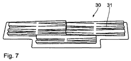
図6は、反射面29からの形成及びそこからのその後の分離の後の減衰器半物品30を示している。形成中及び減衰器半物品30から生成されたEUV減衰器27の後の作動位置において反射面29に対面する減衰器面31は閲覧者に向く。図7は、減衰器面31の反対側から見た減衰器半物品30を示している。
FIG. 6 shows the
図6は、高精度に傾斜され、凹に設計された視野ファセット19の輪郭を減衰器面31が用いていることを示している。
FIG. 6 shows that the
電気メッキ形成に続く段階では、補正照明視野ファセット19Kに関連付けられるEUV絞り24は、この時点で、関連付けられるそれぞれの絞り輪郭25を伴って生成される。この生成は、例えば、レーザ材料除去法又はワイヤ腐食を用いて行うことができる。
In the stage following electroplating formation, an
その結果は、図8に示しているEUV減衰器27の区画である。図1は、視野ファセットミラー13の前にあるEUV減衰器27の配列を略示している。EUV減衰器27の場合には、電気メッキによって視野ファセットミラー13の全半分を形成することによって生成された半物品を仮定している。図8には、EUV減衰器27のEUV絞り24の絞り輪郭25を矩形開口部として略示している。実際には、補正照明視野ファセット19Kにおける絞り輪郭25は、例えば、図3に示している形状を有する。個別EUV絞り24は、フレーム31aによって保持することができる。この場合、視野ファセットミラー13から構成される個別ファセット群に関連付けられたEUV絞り24の群に対して、EUV絞り24のこれらの群を保持する個別フレーム要素を設けることができる。絞り31a又は個別フレーム要素は、EUV減衰器27を視野ファセットミラー13の支持体上に装着するための保持構造を有することができる。
The result is a section of the
基本照明視野ファセット19Gは、これらの基本照明視野ファセット19Gの反射面にわたって延びる関連付けられた貫通開口部32を有する。図8に示している概略図では、貫通開口部32は、EUV絞り24の絞り輪郭25と形状が異ならない。
Basic
EUV減衰器27の隣接するEUV絞り24と貫通開口部32とは、これらの間に、格子状のEUV減衰器27において自己支持安定性を保証する補強物33を有する。
The
図9は、図9の視野ファセットミラー13の左手半分の反射面29に隣接して配置された図8に示しているEUV減衰器27を有する視野ファセットミラー13を示している。EUV減衰器27は、電気メッキによって視野ファセットミラー13のこの左手半分に精密に形成することによって生成されたものであるから、視野ファセットミラー13に接触することなく、その極めて近くに持ってくることができる。実際には、反射面29と減衰器面31の間に約100μmの間隔を生成することができる。反射面29と減衰器面31の間の間隔は200μmよりも大きくない。
FIG. 9 shows the
EUV減衰器27と視野ファセットミラー13の間のこの短い間隔は、視野ファセットミラー13の視野ファセット19上へのEUV放射線10の入射角がゼロとは異なることに起因する、絞り輪郭25又は貫通開口部32の境界における望ましくない二重通過損失が阻止されるか、又は最小限に低減されることを意味する。
This short distance between the
図9は、補強物33が、個別ファセット19の間の間隙空間及びファセットブロック20の間の距離区画34に隣接し、これらと平行に延びる補強支柱の形態にあることを示している。従って、補強物又は補強支柱33は、有用EUV放射線10の損失を実質的にもたらされない。
FIG. 9 shows that the
個別絞り輪郭25を有するEUV絞り24を有するEUV減衰器27の改良に対する変形として、EUV減衰器27の上述の例示的な実施形態のEUV絞り24の位置における個別灰色フィルタ設計を用いても補正照明視野ファセット19Kの個別減衰を得ることができる。EUV絞り24の位置に使用される灰色フィルタは、例えば、可変厚みを有する吸収体層とすることができる。代替的又は追加的に、灰色フィルタ区画の上に吸収点構造の規定の分布を与えることができ、x方向、すなわち、長視野軸の方向のその減衰プロフィールは、上述のEUV絞り24のものに対応する。
As a modification to the improvement of the
次に、図10から図13を用いて、EUV減衰器27の代わりに又はそれに加えて使用することができる更に別の変形のEUV減衰器35を説明する。図1から図9を参照して上述したものに対応する構成要素及び機能は同じ参照番号を有し、これらに対しては再度詳細には解説しない。
Next, another modified EUV attenuator 35 that can be used in place of or in addition to the
図10は、図4に示している視野ファセットミラー13の視野ファセットブロック20のうちの1つを示している。この視野ファセットブロック20は、それに関連付けられ、視野ファセットブロック20の補正照明視野ファセット19Kにおける減衰器区画として使用されるEUV減衰器35を有する。
FIG. 10 shows one of the field facet blocks 20 of the
EUV減衰器35は、複数の減衰器指状体を有する。図10は、図10の上部から下部に増加する順序で番号が振られた合計で4つの減衰器指状体36、37、38、及び39を示している。減衰器指状体36から39の各々は、それに関連付けられた補正照明視野ファセット19Kに対する絞りである。減衰器指状体36から39は、これらに関連付けられた補正照明視野ファセット19Kの反射面29から一定の間隔Aの位置で延びている。図10から図13に図示の実施形態では、減衰器指状体36から38と、関連付けられた補正照明視野ファセット19Kの間の間隔Aも同様に200μmよりも大きくない。
The EUV attenuator 35 has a plurality of attenuator fingers. FIG. 10 shows a total of four
視野ファセットブロック20の補正照明視野ファセット19Kは、その反射面29において、x−y平面に対し、すなわち、視野ファセットミラー13の主平面に対するそれぞれの個別傾斜角を有する。減衰器指状体37に関連付けられた補正照明視野ファセット19Kは、図11の左上から右下に傾斜して延びている。減衰器指状体38に関連付けられた補正照明視野ファセット19Kは、図12の左下から右上に傾斜して延びている。この傾斜角に基づいて、瞳ファセットミラー14の関連付けられたそれぞれの瞳ファセット22が、それぞれの補正照明視野ファセット19Kによる反射を受けて照明される。
The corrected
減衰器指状体36から39は、ワイヤ状金属指状体の形態にあるとすることができる。図10の平面図でx方向に直線で延びるように示している遮蔽縁部40は、図1から図9に関連して上述した補正照明を得るようにx−y内で個別に形づくるか又は成形することができる。遮蔽縁部は、レーザ材料加工、ワイヤ腐食、又はフォトエッチングによって形づくることができる。 Attenuator fingers 36-39 may be in the form of wire-like metal fingers. 10 may be individually shaped in xy so as to obtain the corrected illumination described above in connection with FIGS. 1-9, or shown as extending straight in the x-direction in the plan view of FIG. Can be molded. The shielding edge can be shaped by laser material processing, wire erosion, or photoetching.
補正照明ファセット19Kの各々は、それに関連付けられた減衰器指状体36から39のうちの厳密に1つを有することができ、この減衰器指状体は、例えば、関連付けられた補正照明視野ファセット19Kの反射面29のy座標軸に見た中心区画を遮蔽する。複数の減衰器指状体36から39を視野ファセットブロック20の補正照明視野ファセット19Kのうちの厳密に1つに関連付けることができる。減衰器指状体36から39のうちの2つを補正照明視野ファセット19Kのうちの厳密に1つに関連付けることができる。
Each of the
減衰器指状体36から38は、共通の装着支持体41によって担持される。装着支持体41は、2つの支持ブラケット42、43を有する。2つの支持ブラケット42、43は、ファセットブロック20の両側に配置される。減衰器指状体36から39は、2つの支持ブラケット42、43の間に延びている。
減衰器指状体36から39に対する支持ブラケット42、43上の保持点は、支持ブラケット42、43内の支持溝44によって形成される。補正照明視野ファセット19Kの反射面29の傾斜した外形に従って支持溝44の深さは、関連付けられる減衰器指状体36から39に対して設計される。減衰器指状体36から39の端部は、それぞれ、関連付けられた支持溝44の基部上に支持される。減衰器指状体36から39は、例えば、関連付けられた支持体溝44の基部に接合することができる。減衰器指状体37では、図11及び図12の左に示している支持ブラケット42内の支持溝44はごく小さい深さのものであり、それに対して図11及び図12の右に示している支持ブラケット43内の支持溝44は非常に大きい深さを有する。減衰器指状体38では、支持ブラケット42内の支持溝44は大きい深さのものであり、支持ブラケット43内の支持溝44は小さい深さのものである。境界にある2つの減衰器指状体36、39では、減衰器指状体36、39が、関連付けられた補正照明視野ファセット19Kの反射面29と同様にx方向と平行に延びるように、平均深さの支持溝44が設けられる。従って、支持溝44、すなわち、減衰器指状体36から39に対する支持ブラケット42、43上の保持点は、張られる補正照明個別ファセット19Kの形状に依存するレベルに配置される。
The holding points on the
支持ブラケット42、43は、図10に示している視野ファセットブロック20と、x方向に隣接してそれに続く視野ファセットブロック(図示せず)の間に挿入される。
The
照明補正は、照明光学系4を用いて以下の通りに実施される。最初に適切な検出器を用いて、物体視野5の照明における強度分布が確認される。更に、物体視野5の照明における角度分布を測定することができる。この測定結果を用いて、補正照明視野ファセット19Kの設計が計算される。次に、計算された設計及び関連付けが照明光学系4内に与えられ、これは、例えば、使用される補正照明視野ファセット19Kを特定的に選択することによって行うことができる。その後に、レチクルと照明光10に対して感光性を有するコーティングを保持するウェーハとが準備される段階、更に、投影露光装置1を用いてレチクルのうちの少なくとも1つの区画がウェーハ上に投影される段階を含む投影露光が行われる。最後に、照明光ビーム10に露光された感光層がウェーハ上で現像される。
The illumination correction is performed using the illumination optical system 4 as follows. First, using an appropriate detector, the intensity distribution in the illumination of the
上述の補正照明視野ファセットの様々な変形は、これらの補正照明視野ファセットのビーム誘導作用を動的に制御するのに使用することができる。この目的のために、補正照明視野ファセットは、投影露光装置内の制御デバイスによって作動させることができる。この作動は、物体視野又はそうでなければ像視野内の長視野寸法にわたる強度プロフィールの測定に基づいて行うことができる。 Various variations of the corrected illumination field facets described above can be used to dynamically control the beam guidance effects of these corrected illumination field facets. For this purpose, the correction illumination field facet can be actuated by a control device in the projection exposure apparatus. This operation can be based on the measurement of intensity profiles over long field dimensions in the object field or otherwise in the image field.
視野ファセットミラー13が補正照明視野ファセットを伴って作動され、特にこれらのファセットが能動的に再配置可能又は能動的に遮蔽可能な形態にある場合には、個別補正照明視野ファセット又は補正照明視野ファセットの群は、接続又は接断することができる。
The individual correction illumination field facets or correction illumination field facets are operated when the
上述したものとは異なる実施形態の補正照明視野ファセットは、物体視野の部分領域のみを照明することを可能にする。この部分領域照明は、特定の視野レベル、すなわち、視野の部分領域において補正照明視野ファセットによって与えられる照明光を混入させる結果として、これらの視野レベルにおける強度の落ち込みを均等化するのに使用することができる。 Different embodiments of the corrected illumination field facets different from those described above make it possible to illuminate only a partial region of the object field. This partial area illumination should be used to equalize the intensity drop at these field levels as a result of mixing in the illumination light provided by the correct illumination field facet at a certain field level, i.e. a partial area of the field of view. Can do.
上述したものとは異なる実施形態の補正照明視野ファセットの実質的に照明される領域の縁部形状は、少なくとも1つの変向点を有することができる。この縁部は、補正照明視野ファセットの高反射領域と低効率反射領域又は非反射領域の間の分割線とすることができる。少なくとも1つの変向点を有する縁部は、物理的に存在するファセット縁部とすることができる。この縁部は、適切に成形された遮蔽本体によって生成することができる。 The edge shape of the substantially illuminated region of the correction illumination field facet of the different embodiment from that described above may have at least one turning point. This edge may be a dividing line between the high reflection area and the low efficiency reflection area or non-reflection area of the corrected illumination field facet. An edge having at least one turning point may be a physically present facet edge. This edge can be produced by a suitably shaped shielding body.
13 視野ファセットミラー
20 視野ファセットブロック
27 EUV減衰器
31a フレーム
33 補強物
34 距離区画
13
Claims (23)
照明光ビーム(10)を形成するための非平面ミラー表面形状を備えた反射面(29)を有する少なくとも1つのEUVミラー(13)を有し、
前記EUVミラー(13)の前に配置された少なくとも1つのEUV減衰器(27)であって、該EUV減衰器(27)の該EUVミラー(13)の前記反射面(29)に対面する減衰器面(31)が、前記ミラー表面形状を補完するように設計された減衰器表面形状を有し、それによって該減衰器面(31)のうちの少なくともある一定の区画が、該反射面(29)に接触することなく該反射面(29)から一定の間隔の位置に配置される少なくとも1つのEUV減衰器(27)を有する、
ことを特徴とする照明光学系。 Illumination optics (4) for EUV microlithography for directing an illumination light beam (10) from a radiation source (3) to an object field (5),
Having at least one EUV mirror (13) having a reflective surface (29) with a non-planar mirror surface shape for forming an illumination light beam (10);
At least one EUV attenuator (27) disposed in front of the EUV mirror (13), the attenuation facing the reflective surface (29) of the EUV mirror (13) of the EUV attenuator (27) The vessel surface (31) has an attenuator surface shape designed to complement the mirror surface shape so that at least certain sections of the attenuator surface (31) have the reflective surface ( 29) having at least one EUV attenuator (27) arranged at a regular distance from the reflecting surface (29) without contacting the
An illumination optical system characterized by that.
請求項1から請求項19のいずれか1項に記載の照明光学系(4)を有する、
ことを特徴とする照明系。 An EUV radiation source (3) for generating an illumination light beam (10);
The illumination optical system (4) according to any one of claims 1 to 19,
An illumination system characterized by that.
物体視野(5)を像視野(8)上に投影するための投影光学系(7)を有する、
ことを特徴とする投影露光装置。 An illumination system according to claim 21,
A projection optical system (7) for projecting the object field (5) onto the image field (8);
A projection exposure apparatus.
レチクルが準備される段階と、
照明光(10)に対して感光性を有するコーティングを有するウェーハが準備される段階と、
請求項22に記載の投影露光装置を用いて前記レチクルの少なくとも1つの区画が前記ウェーハ上に投影される段階と、
前記照明光ビーム(10)に露光された前記感光層が前記ウェーハ上で現像される段階と、
を有することを特徴とする方法。 A method for producing a microstructured component, comprising:
The stage where the reticle is prepared,
Providing a wafer having a coating photosensitive to illumination light (10);
Projecting at least one section of the reticle onto the wafer using the projection exposure apparatus of claim 22;
Developing the photosensitive layer exposed to the illumination light beam (10) on the wafer;
A method characterized by comprising:
Applications Claiming Priority (1)
| Application Number | Priority Date | Filing Date | Title |
|---|---|---|---|
| PCT/EP2009/002247 WO2010108516A1 (en) | 2009-03-27 | 2009-03-27 | Illumination optical system for euv microlithography and euv attenuator for an illumination optical system of this kind, illumination system and projection exposure installation having an illumination optical system of this kind |
Publications (3)
| Publication Number | Publication Date |
|---|---|
| JP2012522358A JP2012522358A (en) | 2012-09-20 |
| JP2012522358A5 JP2012522358A5 (en) | 2016-09-15 |
| JP6041304B2 true JP6041304B2 (en) | 2016-12-07 |
Family
ID=41403048
Family Applications (1)
| Application Number | Title | Priority Date | Filing Date |
|---|---|---|---|
| JP2012501137A Active JP6041304B2 (en) | 2009-03-27 | 2009-03-27 | Illumination optical system for EUV microlithography, EUV attenuator for this type of illumination optical system, and illumination system and projection exposure apparatus having this type of illumination optical system |
Country Status (4)
| Country | Link |
|---|---|
| US (1) | US9482959B2 (en) |
| JP (1) | JP6041304B2 (en) |
| CN (1) | CN102365587B (en) |
| WO (1) | WO2010108516A1 (en) |
Families Citing this family (10)
| Publication number | Priority date | Publication date | Assignee | Title |
|---|---|---|---|---|
| DE102012207377A1 (en) * | 2012-05-03 | 2013-11-07 | Carl Zeiss Smt Gmbh | Illumination optics and optical system for EUV projection lithography |
| DE102012210174A1 (en) * | 2012-06-18 | 2013-06-06 | Carl Zeiss Smt Gmbh | Optical component for use in illumination optics of illumination system of projection exposure system for guiding light radiation to object field, has individual mirrors with front side that forms individual mirror reflecting surface |
| CN108873623B (en) | 2013-06-18 | 2021-04-06 | Asml荷兰有限公司 | Lithographic method and lithographic system |
| DE102013218131A1 (en) * | 2013-09-11 | 2015-03-12 | Carl Zeiss Smt Gmbh | Illumination optics and illumination system for EUV projection lithography |
| DE102013218749A1 (en) * | 2013-09-18 | 2015-03-19 | Carl Zeiss Smt Gmbh | Illumination system and illumination optics for EUV projection lithography |
| US9575412B2 (en) * | 2014-03-31 | 2017-02-21 | Taiwan Semiconductor Manufacturing Company, Ltd. | Method and system for reducing pole imbalance by adjusting exposure intensity |
| DE102017211443A1 (en) * | 2017-07-05 | 2019-01-10 | Carl Zeiss Smt Gmbh | Metrology system with an EUV look |
| DE102019202868A1 (en) * | 2019-03-04 | 2020-09-10 | Carl Zeiss Smt Gmbh | Actuator device and method for aligning an optical element, optical assembly and projection exposure system |
| DE102019206867A1 (en) | 2019-05-13 | 2019-07-11 | Carl Zeiss Smt Gmbh | Optical element for a projection exposure machine |
| DE102019206868A1 (en) | 2019-05-13 | 2019-07-04 | Carl Zeiss Smt Gmbh | Field facet mirror for illumination optics of a projection exposure apparatus |
Family Cites Families (16)
| Publication number | Priority date | Publication date | Assignee | Title |
|---|---|---|---|---|
| DE10138313A1 (en) | 2001-01-23 | 2002-07-25 | Zeiss Carl | Collector for lighting systems with a wavelength <193 nm |
| DE19955984A1 (en) | 1999-11-20 | 2001-05-23 | Zeiss Carl | Optical imaging device, in particular objective with at least one system aperture |
| DE60326063D1 (en) * | 2002-03-18 | 2009-03-19 | Asml Netherlands Bv | Lithographic apparatus and method for making an article |
| US7333178B2 (en) * | 2002-03-18 | 2008-02-19 | Asml Netherlands B.V. | Lithographic apparatus and device manufacturing method |
| JP3809817B2 (en) * | 2002-12-19 | 2006-08-16 | 株式会社村田製作所 | Dielectric filter, dielectric duplexer, and communication device |
| JPWO2004068564A1 (en) * | 2002-12-26 | 2006-05-25 | 株式会社ニコン | Illumination optical system, illumination apparatus, projection exposure apparatus, and exposure method |
| JP4356695B2 (en) * | 2003-05-09 | 2009-11-04 | 株式会社ニコン | Illumination optical system, projection exposure apparatus, and microdevice manufacturing method |
| ATE502323T1 (en) | 2003-07-30 | 2011-04-15 | Zeiss Carl Smt Gmbh | ILLUMINATION SYSTEM FOR MICROLITHOGRAPHY |
| US7023524B2 (en) * | 2003-12-18 | 2006-04-04 | Asml Netherlands B.V. | Lithographic apparatus and device manufacturing method |
| JP2006128321A (en) * | 2004-10-27 | 2006-05-18 | Nikon Corp | Manufacturing method of illumination optical system, aligner and micro device |
| EP1894063A1 (en) * | 2005-06-21 | 2008-03-05 | Carl Zeiss SMT AG | A double-facetted illumination system with attenuator elements on the pupil facet mirror |
| WO2007093433A1 (en) * | 2006-02-17 | 2007-08-23 | Carl Zeiss Smt Ag | Illumination system for microlithographic projection exposure apparatus comprising an illumination system of this type |
| KR20090013746A (en) | 2006-05-25 | 2009-02-05 | 가부시키가이샤 니콘 | Illuminating optical apparatus, exposure apparatus, and device manufacturing method |
| US7990520B2 (en) * | 2006-12-18 | 2011-08-02 | Carl Zeiss Smt Gmbh | Microlithography illumination systems, components and methods |
| DE102007061194A1 (en) * | 2006-12-18 | 2008-06-19 | Carl Zeiss Smt Ag | Illumination system for extreme ultraviolet micro lithograph, has illumination optic for guiding illuminating light of radiation source into object field in object plane |
| JP4962203B2 (en) | 2007-08-08 | 2012-06-27 | 株式会社ニコン | EUV exposure apparatus, exposure method, and device manufacturing method |
-
2009
- 2009-03-27 JP JP2012501137A patent/JP6041304B2/en active Active
- 2009-03-27 CN CN200980158506.2A patent/CN102365587B/en active Active
- 2009-03-27 WO PCT/EP2009/002247 patent/WO2010108516A1/en active Application Filing
-
2011
- 2011-09-01 US US13/223,458 patent/US9482959B2/en active Active
Also Published As
| Publication number | Publication date |
|---|---|
| CN102365587B (en) | 2015-07-22 |
| US20120069313A1 (en) | 2012-03-22 |
| JP2012522358A (en) | 2012-09-20 |
| US9482959B2 (en) | 2016-11-01 |
| CN102365587A (en) | 2012-02-29 |
| WO2010108516A1 (en) | 2010-09-30 |
Similar Documents
| Publication | Publication Date | Title |
|---|---|---|
| JP6041304B2 (en) | Illumination optical system for EUV microlithography, EUV attenuator for this type of illumination optical system, and illumination system and projection exposure apparatus having this type of illumination optical system | |
| TWI468838B (en) | Imaging optical system and projection exposure installation for microlithography with an imaging optical system of this type | |
| JP5938043B2 (en) | Imaging optics | |
| JP5385970B2 (en) | Illumination optical system for EUV microlithography, illumination system including this kind of illumination optical system, and projection exposure apparatus | |
| TWI714524B (en) | Illumination optical unit for projection lithography, pupil facet mirror, optical system, illumination system, projection exposure apparatus, method for producing a microstructured component, and microstructured component | |
| JP5717513B2 (en) | Illumination optics for projection lithography | |
| JP5077724B2 (en) | Reflective illumination system for microlithography tools | |
| TWI539241B (en) | Mirror | |
| JP6221160B2 (en) | Mirror placement | |
| KR19990088055A (en) | Illumination System Particularly For EUV Lithography | |
| TWI461733B (en) | Imaging optical system, projection exposure installation for microlithography with an imaging optical system of this type and method for producing a structured component | |
| CN116249919A (en) | Digital micromirror device for illumination optics of projection exposure system | |
| JP2015052797A (en) | Imaging optics and projection exposure device for microlithography with imaging optics of this type | |
| US10928733B2 (en) | Illumination optic for projection lithography | |
| WO2017046136A1 (en) | Illumination optical unit for projection lithography | |
| TW202343152A (en) | Method for measuring an illumination angle distribution on an object field and illumination optics unit having an illumination channel allocation intended therefor | |
| TW201626111A (en) | Illumination optical unit for illuminating an illumination field and projection exposure apparatus comprising such an illumination optical unit |
Legal Events
| Date | Code | Title | Description |
|---|---|---|---|
| A977 | Report on retrieval |
Free format text: JAPANESE INTERMEDIATE CODE: A971007 Effective date: 20130612 |
|
| A131 | Notification of reasons for refusal |
Free format text: JAPANESE INTERMEDIATE CODE: A131 Effective date: 20130619 |
|
| A601 | Written request for extension of time |
Free format text: JAPANESE INTERMEDIATE CODE: A601 Effective date: 20130919 |
|
| A602 | Written permission of extension of time |
Free format text: JAPANESE INTERMEDIATE CODE: A602 Effective date: 20130927 |
|
| A521 | Request for written amendment filed |
Free format text: JAPANESE INTERMEDIATE CODE: A523 Effective date: 20131219 |
|
| A02 | Decision of refusal |
Free format text: JAPANESE INTERMEDIATE CODE: A02 Effective date: 20140226 |
|
| A601 | Written request for extension of time |
Free format text: JAPANESE INTERMEDIATE CODE: A601 Effective date: 20150825 |
|
| A521 | Request for written amendment filed |
Free format text: JAPANESE INTERMEDIATE CODE: A523 Effective date: 20151125 |
|
| A601 | Written request for extension of time |
Free format text: JAPANESE INTERMEDIATE CODE: A601 Effective date: 20160427 |
|
| A601 | Written request for extension of time |
Free format text: JAPANESE INTERMEDIATE CODE: A601 Effective date: 20160627 |
|
| A524 | Written submission of copy of amendment under article 19 pct |
Free format text: JAPANESE INTERMEDIATE CODE: A524 Effective date: 20160727 |
|
| A61 | First payment of annual fees (during grant procedure) |
Free format text: JAPANESE INTERMEDIATE CODE: A61 Effective date: 20161101 |
|
| R150 | Certificate of patent or registration of utility model |
Ref document number: 6041304 Country of ref document: JP Free format text: JAPANESE INTERMEDIATE CODE: R150 |
|
| R250 | Receipt of annual fees |
Free format text: JAPANESE INTERMEDIATE CODE: R250 |
|
| R250 | Receipt of annual fees |
Free format text: JAPANESE INTERMEDIATE CODE: R250 |
|
| R250 | Receipt of annual fees |
Free format text: JAPANESE INTERMEDIATE CODE: R250 |
|
| R250 | Receipt of annual fees |
Free format text: JAPANESE INTERMEDIATE CODE: R250 |
|
| R250 | Receipt of annual fees |
Free format text: JAPANESE INTERMEDIATE CODE: R250 |