JP6018051B2 - Light redirecting film and display system incorporating the same - Google Patents
Light redirecting film and display system incorporating the same Download PDFInfo
- Publication number
- JP6018051B2 JP6018051B2 JP2013512658A JP2013512658A JP6018051B2 JP 6018051 B2 JP6018051 B2 JP 6018051B2 JP 2013512658 A JP2013512658 A JP 2013512658A JP 2013512658 A JP2013512658 A JP 2013512658A JP 6018051 B2 JP6018051 B2 JP 6018051B2
- Authority
- JP
- Japan
- Prior art keywords
- film
- optical
- less
- item
- structured surface
- Prior art date
- Legal status (The legal status is an assumption and is not a legal conclusion. Google has not performed a legal analysis and makes no representation as to the accuracy of the status listed.)
- Expired - Fee Related
Links
Images


Classifications
-
- G—PHYSICS
- G02—OPTICS
- G02B—OPTICAL ELEMENTS, SYSTEMS OR APPARATUS
- G02B5/00—Optical elements other than lenses
- G02B5/04—Prisms
-
- G—PHYSICS
- G02—OPTICS
- G02B—OPTICAL ELEMENTS, SYSTEMS OR APPARATUS
- G02B1/00—Optical elements characterised by the material of which they are made; Optical coatings for optical elements
- G02B1/10—Optical coatings produced by application to, or surface treatment of, optical elements
-
- G—PHYSICS
- G02—OPTICS
- G02B—OPTICAL ELEMENTS, SYSTEMS OR APPARATUS
- G02B5/00—Optical elements other than lenses
- G02B5/02—Diffusing elements; Afocal elements
- G02B5/0205—Diffusing elements; Afocal elements characterised by the diffusing properties
- G02B5/021—Diffusing elements; Afocal elements characterised by the diffusing properties the diffusion taking place at the element's surface, e.g. by means of surface roughening or microprismatic structures
- G02B5/0221—Diffusing elements; Afocal elements characterised by the diffusing properties the diffusion taking place at the element's surface, e.g. by means of surface roughening or microprismatic structures the surface having an irregular structure
-
- G—PHYSICS
- G02—OPTICS
- G02B—OPTICAL ELEMENTS, SYSTEMS OR APPARATUS
- G02B5/00—Optical elements other than lenses
-
- G—PHYSICS
- G02—OPTICS
- G02B—OPTICAL ELEMENTS, SYSTEMS OR APPARATUS
- G02B5/00—Optical elements other than lenses
- G02B5/02—Diffusing elements; Afocal elements
- G02B5/0205—Diffusing elements; Afocal elements characterised by the diffusing properties
- G02B5/0236—Diffusing elements; Afocal elements characterised by the diffusing properties the diffusion taking place within the volume of the element
- G02B5/0242—Diffusing elements; Afocal elements characterised by the diffusing properties the diffusion taking place within the volume of the element by means of dispersed particles
-
- G—PHYSICS
- G02—OPTICS
- G02B—OPTICAL ELEMENTS, SYSTEMS OR APPARATUS
- G02B5/00—Optical elements other than lenses
- G02B5/02—Diffusing elements; Afocal elements
- G02B5/0268—Diffusing elements; Afocal elements characterized by the fabrication or manufacturing method
-
- G—PHYSICS
- G02—OPTICS
- G02B—OPTICAL ELEMENTS, SYSTEMS OR APPARATUS
- G02B5/00—Optical elements other than lenses
- G02B5/02—Diffusing elements; Afocal elements
- G02B5/0273—Diffusing elements; Afocal elements characterized by the use
- G02B5/0278—Diffusing elements; Afocal elements characterized by the use used in transmission
Landscapes
- Physics & Mathematics (AREA)
- General Physics & Mathematics (AREA)
- Optics & Photonics (AREA)
- Chemical & Material Sciences (AREA)
- Dispersion Chemistry (AREA)
- Engineering & Computer Science (AREA)
- Manufacturing & Machinery (AREA)
- Optical Elements Other Than Lenses (AREA)
- Laminated Bodies (AREA)
- Devices For Indicating Variable Information By Combining Individual Elements (AREA)
Description
本説明は、一般に光の方向を転換するための光学フィルムに関する。本説明は、かかる光学フィルムを組み込んだ、ディスプレイシステムなどの光学システムに更に適用可能である。 This description relates generally to an optical film for changing the direction of light. The description is further applicable to optical systems, such as display systems, that incorporate such optical films.
液晶ディスプレイ(LCD)システムなどのディスプレイシステムは様々な用途で用いられており、例えば、コンピュータ用モニター、携帯情報端末(PDA)、携帯電話、小型音楽プレーヤー、及び薄型LCDテレビなどの市販の装置である。大部分のLCDは、液晶パネルと、液晶パネルを照射するための拡張範囲型光源(バックライトと呼ばれることが多い)と、を含む。バックライトは、典型的に、1つ以上のランプと、多数の光管理フィルム(例えば、光ガイド、ミラーフィルム、光方向転換フィルム、リターダーフィルム、光偏光フィルム、及び拡散フィルム)と、を含む。拡散フィルムは、典型的に、光学的欠陥を隠蔽し、バックライトによって放射された光の輝度均一性を向上させるために含まれる。 Display systems such as liquid crystal display (LCD) systems are used in a variety of applications, such as commercially available devices such as computer monitors, personal digital assistants (PDAs), cell phones, small music players, and thin LCD televisions. is there. Most LCDs include a liquid crystal panel and an extended range light source (often called a backlight) for illuminating the liquid crystal panel. The backlight typically includes one or more lamps and a number of light management films (eg, light guides, mirror films, light redirecting films, retarder films, light polarizing films, and diffusing films). A diffusing film is typically included to conceal optical defects and improve the brightness uniformity of the light emitted by the backlight.
一態様では、本説明は、構造化表面を有する光学フィルムに関する。この光学フィルムは、約10%未満の光学的ヘイズ及び約50%未満の光学的透明度を有する。このフィルムの構造化表面の少なくとも85%は、約7.5度未満である勾配規模を有する。 In one aspect, the present description relates to an optical film having a structured surface. The optical film has an optical haze of less than about 10% and an optical clarity of less than about 50%. At least 85% of the structured surface of the film has a gradient magnitude that is less than about 7.5 degrees.
別の態様では、本発明は、構造化表面を有する光学フィルムに関する。この光学フィルムは、約7.5%未満の光学的ヘイズ及び約60%未満の光学的透明度を有する。このフィルムの構造化表面の少なくとも90%は、約7.5度未満である勾配規模を有する。また、このフィルムは、その一部が約0.5マイクロメートル未満である平均寸法を有する複数の粒子からなる。 In another aspect, the invention relates to an optical film having a structured surface. The optical film has an optical haze of less than about 7.5% and an optical clarity of less than about 60%. At least 90% of the structured surface of the film has a gradient magnitude that is less than about 7.5 degrees. The film also consists of a plurality of particles having an average dimension, a portion of which is less than about 0.5 micrometers.
第3の態様では、本説明は、構造化表面を有する光学フィルムに関する。この光学フィルムは、約5%未満の光学的ヘイズ及び約70%未満の光学的透明度を有する。このフィルムの構造化表面の少なくとも85%は、約5度未満である勾配規模を有する。またこのフィルムは、その一部が約0.5マイクロメートル未満の平均寸法を有する複数の粒子からなる。 In a third aspect, the present description relates to an optical film having a structured surface. The optical film has an optical haze of less than about 5% and an optical clarity of less than about 70%. At least 85% of the structured surface of the film has a gradient magnitude that is less than about 5 degrees. The film also consists of a plurality of particles, some of which have an average dimension of less than about 0.5 micrometers.
別の態様では、本説明は、構造化表面を有する光学フィルムに関する。この光学フィルムは、約3%未満の光学的ヘイズ及び約65%未満の光学的透明度を有する。このフィルムの構造化表面の少なくとも90%は、約5度未満である勾配規模を有する。 In another aspect, the present description relates to an optical film having a structured surface. The optical film has an optical haze of less than about 3% and an optical clarity of less than about 65%. At least 90% of the structured surface of the film has a gradient magnitude that is less than about 5 degrees.
更に別の態様では、本説明は、構造化表面を有する光学フィルムに関する。この光学フィルムは、約1.5%未満の光学的ヘイズ及び約80%未満の光学的透明度を有する。このフィルムの構造化表面の少なくとも80%は、約2.5度未満である勾配規模を有する。 In yet another aspect, the present description relates to an optical film having a structured surface. The optical film has an optical haze of less than about 1.5% and an optical clarity of less than about 80%. At least 80% of the structured surface of the film has a gradient magnitude that is less than about 2.5 degrees.
別の態様では、本説明は、構造化表面を有する光学フィルムに関する。この光学フィルムは、約1%未満の光学的ヘイズ及び約90%未満の光学的透明度を有する。このフィルムの構造化表面の少なくとも90%は、約4度未満である勾配規模を有する。 In another aspect, the present description relates to an optical film having a structured surface. The optical film has an optical haze of less than about 1% and an optical clarity of less than about 90%. At least 90% of the structured surface of the film has a gradient magnitude that is less than about 4 degrees.
別の態様では、本説明は、構造化表面を有する光学フィルムに関する。この光学フィルムは、約20%未満の光学的ヘイズ及び約40%未満の光学的透明度を有する。このフィルムの構造化表面の少なくとも90%は、約10度未満である勾配規模を有する。 In another aspect, the present description relates to an optical film having a structured surface. The optical film has an optical haze of less than about 20% and an optical clarity of less than about 40%. At least 90% of the structured surface of the film has a gradient magnitude that is less than about 10 degrees.
更なる一態様では、本説明は、第1及び第2の構造化表面を有する光学フィルムに関する。第1の構造化表面は複数のプリズム構造を有し、第2の構造化表面は第1の構造化表面に対向し、複数のミクロ構造を有する。フィルムの実効透過率は、平滑で、構造化されていない第2の表面を除いて同等の構造を備えるフィルムよりも、最大で1%低い。 In a further aspect, the present description relates to an optical film having first and second structured surfaces. The first structured surface has a plurality of prism structures, and the second structured surface is opposite the first structured surface and has a plurality of microstructures. The effective transmittance of the film is up to 1% lower than a film with a smooth structure and equivalent structure except for the unstructured second surface.
別個の態様では、本説明は、第1の光学フィルムと、第1の光学フィルム上に配置された第2の光学フィルムと、を有し、第2の光学フィルムが第1の光学フィルムに光学的に結合されている、光学フィルム積層体に関する。第2の光学フィルムは、構造化表面を有する。フィルム積層体の実効透過率は、構造化表面ではなく、平滑な表面を有する第2の光学フィルムを除いて同等の構造を備えるフィルム積層体よりも最大で1%低い。 In a separate aspect, the description includes a first optical film and a second optical film disposed on the first optical film, the second optical film being optical to the first optical film. It is related with the optical film laminated body currently couple | bonded. The second optical film has a structured surface. The effective transmittance of the film laminate is up to 1% lower than a film laminate having an equivalent structure except for the second optical film having a smooth surface rather than a structured surface.
別の態様では、本説明は、その表面に不規則に分布する複数のミクロ構造を有する光学フィルムに関する。この光学フィルムの表面の50%は、約1度〜5度の勾配を有する。 In another aspect, the present description relates to an optical film having a plurality of microstructures randomly distributed on its surface. 50% of the surface of the optical film has a gradient of about 1-5 degrees.
別の態様では、本説明は、構造化表面を有する光学フィルムに関する。このフィルムは、約75%〜95%の光学的透明度及び約0〜1%の光学的ヘイズを有する。この光学フィルムは、約0.5マイクロメートル未満の平均寸法を備える複数の粒子を有する。 In another aspect, the present description relates to an optical film having a structured surface. The film has an optical clarity of about 75% to 95% and an optical haze of about 0 to 1%. The optical film has a plurality of particles with an average dimension of less than about 0.5 micrometers.
別の態様では、本説明は、構造化表面を有する光学フィルムに関する。このフィルムは、約35%〜70%の光学的透明度及び約1〜4%の光学的ヘイズを有する。 In another aspect, the present description relates to an optical film having a structured surface. The film has an optical clarity of about 35% to 70% and an optical haze of about 1-4%.
別の態様では、本説明は、構造化表面を有する光学フィルムに関する。このフィルムは、約30%〜55%の光学的透明度及び約4〜10%の光学的ヘイズを有する。この光学フィルムは、約0.5マイクロメートル未満の平均寸法を備える複数の粒子を有する。 In another aspect, the present description relates to an optical film having a structured surface. The film has an optical clarity of about 30% -55% and an optical haze of about 4-10%. The optical film has a plurality of particles with an average dimension of less than about 0.5 micrometers.
別の態様では、本説明は、構造化表面を有する光学フィルムに関する。このフィルムは、約25%〜45%の光学的透明度及び約10〜18%の光学的ヘイズを有する。この光学フィルムは、約0.5マイクロメートル未満の平均寸法を備える複数の粒子を有する。 In another aspect, the present description relates to an optical film having a structured surface. The film has an optical clarity of about 25% -45% and an optical haze of about 10-18%. The optical film has a plurality of particles with an average dimension of less than about 0.5 micrometers.
別の態様では、本説明は、ディスプレイを照射するためのバックライトに関する。このバックライトは、光源と、光源から受光するための第1の光学フィルムと、複数のミクロ構造を有する第2の光学フィルムと、を有する。第1の光学フィルムは、第2の光学フィルム上に配置され、第2の光学フィルムに光学的に結合されている。第2のフィルムは、約85%未満の光学的透明度及び約3.5%未満の光学的ヘイズを有する。 In another aspect, the present description relates to a backlight for illuminating a display. This backlight has a light source, a first optical film for receiving light from the light source, and a second optical film having a plurality of microstructures. The first optical film is disposed on the second optical film and optically coupled to the second optical film. The second film has an optical clarity of less than about 85% and an optical haze of less than about 3.5%.
更なる態様では、本説明は、構造化表面を有する光学フィルムに関する。この表面の透明度は、((−3×光学的ヘイズ)+80%)未満である。透明度は、20%超であってもよい。 In a further aspect, the present description relates to an optical film having a structured surface. The transparency of this surface is less than ((−3 × optical haze) + 80%). The transparency may be greater than 20%.
最後の態様では、本説明は、マット仕上げを有するフィルムの作製方法に関する。この方法は、基材上に配置されたコーティング可能な材料を含むコーティングされた基材をもたらすことであって、コーティング可能な材料がコーティングされた基材の第1の主表面をもたらすことを含む。この方法は、コーティング可能な材料の粘度を初期粘度から第2の粘度に変化させることを更に含む。コーティングされた基材に第1のローラーを通過させて、全てのくずを取り除く。コーティングされた基材の第1の主表面に少なくとも1つの表面側ローラーを接触させて、マット仕上げを付与する。所望により、コーティング可能な材料を硬化させて、フィルムをもたらす。 In the last aspect, the description relates to a method of making a film having a matte finish. The method includes providing a coated substrate that includes a coatable material disposed on the substrate, wherein the coatable material provides a first major surface of the coated substrate. . The method further includes changing the viscosity of the coatable material from an initial viscosity to a second viscosity. Pass the first roller through the coated substrate to remove all debris. At least one surface side roller is brought into contact with the first major surface of the coated substrate to provide a matte finish. If desired, the coatable material is cured to provide a film.
本説明は、添付の図面に関連して以下の本説明の種々の実施形態の「発明を実施するための形態」を考慮したとき、より完全に理解し正しく認識され得る。
本説明は、概して、ディスプレイシステム内の輝度を実質的に向上させることができ、一方でそれと同時に、キズなどの物理的欠陥及びモアレ、色むら(color mura)など望ましくない光学的効果を遮蔽及び/又は除去できる光学フィルムに関する。開示される光学フィルムは、ディスプレイにおいて、1つ以上の拡散フィルムなど1つ以上の従来のフィルムの必要性を除去するか、低減する。開示される光学フィルムは、輝度を向上させるために不規則に分布する複数のミクロ構造と、ディスプレイの体裁を向上させるためのマット面と、を含む。マット面は、物理的欠陥、モアレ、色むらの可視性を遮蔽、除去、及び/又は低減し、構造化表面と物理的に接触するフィルムのキズを実質的に除去するか、低減する。構造化表面の光学的ヘイズは輝度を実質的に維持する範囲内であり、構造化表面の光学的透明度は欠陥を実質的に遮蔽及び/又は除去する範囲内である。 This description generally can substantially improve the brightness within the display system, while at the same time masking and eliminating physical defects such as scratches and undesirable optical effects such as moire and color mura. The present invention relates to an optical film that can be removed. The disclosed optical film eliminates or reduces the need for one or more conventional films, such as one or more diffusion films, in a display. The disclosed optical film includes a plurality of irregularly distributed microstructures to improve brightness and a matte surface to improve the appearance of the display. The matte surface masks, eliminates, and / or reduces the visibility of physical defects, moire, and color unevenness, and substantially eliminates or reduces film scratches that physically contact the structured surface. The optical haze of the structured surface is in a range that substantially maintains brightness, and the optical transparency of the structured surface is in a range that substantially masks and / or removes defects.
本説明は、その表面に不規則に配向された複数の構造を有するフィルムに関する。問題の構造は非常に小さい勾配を有し、フィルムは低コストで製造可能である。示されるフィルムは、光学的ヘイズ及び透明度の値を多数有してもよい。これらの値は、所望通りに光学システムの性能を向上させるために、特定のヘイズ及び透明度の値に対して決定されてもよい。 The present description relates to a film having a plurality of structures randomly oriented on its surface. The structure in question has a very small gradient and the film can be manufactured at low cost. The films shown may have a number of optical haze and transparency values. These values may be determined for specific haze and transparency values to improve the performance of the optical system as desired.
図1は、入射光線を所望の方向に方向転換するための光方向転換フィルム100の概略的側面図である。光方向転換フィルム100は、y方向に沿って延在する複数のミクロ構造150を含む第1の構造化表面110を含む。また、光方向転換フィルム100は、第1の構造化表面110の反対側にあって、複数のミクロ構造160を含む第2の構造化表面120を含む。
FIG. 1 is a schematic side view of a
また、光方向転換フィルム100は、それぞれの第1の構造化表面110と第2の構造化表面120との間に配置され、第1の主表面172及び対向する第2の主表面174を含む基材層170も含む。また、光方向転換フィルム100は、基材層の第1の主表面172上に配置され、光方向転換フィルムの第1の構造化表面110を含むプリズム層130と、基材層の第2の主表面174上に配置され、光方向転換フィルムの構造化表面120を含む主表面142を有する構造化層140と、を含む。
The
例示の光方向転換フィルム100は、3つの層130、170、及び140を含む。一般に、光方向転換フィルムは1つ以上の層を有してよい。例えば、幾つかの場合において、光方向転換フィルムは、対応する第1の主表面110と、第2の主表面120と、を含む単一層を有してよい。別の例としては、幾つかの場合において、光方向転換フィルムは多数の層を有してよい。例えば、かかる場合において、基材170は多数の層を有してよい。また、フィルムの様々な層は、別個のフィルムとして理解され得ると理解されてよい。したがって、構造100は、フィルム積層体として理解されてよい。かかる実施形態では、プリズム構造化層130は、第1の光学フィルムとして理解されてよい。同様に、構造化層140は、第1の光学フィルム上に配置され、第1の光学フィルムに光学的に結合される第2の光学フィルムとして理解されてよい。
The exemplary
ミクロ構造150は、主として光方向転換フィルムの主表面120への入射光線を所望の方向に沿って(正のz方向に沿ってなど)方向転換するように設計されている。例示の光方向転換フィルム100では、ミクロ構造150はプリズムの線状構造体である。一般に、ミクロ構造150は、例えば、入射光線の一部を屈折させ、入射光線の別の一部を再利用することによって光を方向転換できる任意の種類のミクロ構造であってよい。例えば、微小構造150の断面形状は湾曲かつ/又は区分的に直線状の部分とするか、これを含んだものとすることができる。例えば、特定の場合では、微小構造150を、y方向に沿って延びる直線状の円筒形レンズとすることができる。
The
各線状プリズムミクロ構造150は、頂角152と、例えば主平面172などの共通基準面から測定された高さ154と、を含む。光結合若しくはウェットアウトを低減させること、及び/又は光方向転換フィルムの耐久性を向上させることが望ましいなど幾つかの場合において、プリズムミクロ構造150の高さは、y方向に沿って変化してよい。例えば、プリズム線状ミクロ構造151のプリズム高さは、y方向に沿って変化する。そのような場合、プリズムミクロ構造151は、y方向に沿って変化する局所的高さと、最大高さ155と、平均高さと、を有する。幾つかの場合において、線状ミクロ構造153などプリズム線状ミクロ構造は、y方向に沿って一定高さを有する。そのような場合、ミクロ構造は、最大高さ及び平均高さと等しい、一定の局所的高さを有する。
Each
光結合又はウェットアウトを低減させることが望ましいなど幾つかの場合において、一部の線状ミクロ構造は低く、一部の線状ミクロ構造は高い。例えば、線状ミクロ構造153の高さ156は、線状ミクロ構造157の高さ158よりも小さい。あるいは、マット層140の表面上のミクロ構造160はまた、光結合又はウェットアウトを低減させるために様々な高さであってよい。
In some cases, such as when it is desirable to reduce optical coupling or wet-out, some linear microstructures are low and some linear microstructures are high. For example, the
頂角、つまり2面角152は、用途において望ましい可能性がある任意の値を有することができる。例えば、幾つかの場合において、頂角152は、約70度〜約110度、又は約80度〜約100度、又は約85度〜約95度の範囲であってよい。幾つかの場合では、ミクロ構造150は、例えば、約88度若しくは89度〜約92度若しくは約91度の範囲であり得る、又は約90度であり得る等しい頂角を有する。
The apex angle, or
プリズム層130は、用途において望ましい可能性がある任意の屈折率を有することができる。例えば、幾つかの場合において、プリズム層の屈折率は、約1.4〜約1.8、又は約1.5〜約1.8、又は約1.5〜約1.7の範囲である。幾つかの場合において、プリズム層の屈折率は、約1.5以上、又は約1.55以上、又は約1.6以上、又は約1.65以上、又は約1.7以上である。
The
光方向転換フィルム100が液晶ディスプレイシステムで用いられるなど幾つかの場合において、光方向転換フィルム100は、ディスプレイの輝度を増大させる、つまり向上させることができる。そのような場合、光方向転換フィルムは、1を超える実効透過率(ET)、つまり相対利得を有する。本明細書で用いるところの「実効透過率」とは、フィルムが所定位置にないディスプレイの輝度に対する、フィルムがディスプレイシステムの定位置に配されたディスプレイシステムの輝度の比のことである。
In some cases, such as when the
実効透過率は、図2に概略的側面図を示す光学システム200を用いて測定できる。光学システム200は、光軸250の中心に配置され、放射面、つまり出射面212を通ってランバート光215を放射する中空のランバートライトボックス210と、線状光吸収偏光子220と、光検出器230と、を含む。ライトボックス210は、光ファイバー270によってライトボックスの内側280に接続された安定化広帯域光源260によって照射される。光学システムの測定対象である試験サンプルのETは、ライトボックスと線状吸収偏光子との間の位置240に配置される。
The effective transmittance can be measured using an
光方向転換フィルム100のETは、線状プリズム150が光検出器に面し、ミクロ構造160がライトボックスに面した状態で、光方向転換フィルムを位置240に配置することによって測定できる。次に、スペクトル的に重み付けされた軸方向輝度I1(光軸250に沿った輝度)が、線状吸収偏光子を通じて光検出器によって測定される。次に、光方向転換フィルムが取り外され、スペクトル的に重み付けされた輝度I2が、光方向転換フィルムを位置240に配置せずに測定される。ETは、比I1/I2である。ET0は、線状プリズム150が線状吸収偏光子220の偏光軸と平行の方向に沿って延在する場合の実効透過率であり、ET90は、線状プリズム150が線状吸収偏光子の偏光軸に対して垂直の方向に沿って延在する場合の実効透過率である。平均実効透過率(ETA)は、ET0とET90との平均である。
The ET of the
本明細書に開示される測定実効透過率値は、光検出器230にSpectraScan(商標)PR−650 SpectraColorimeter(Photo Research,Inc(Chatsworth,CA)から入手可能)を用いて測定した。ライトボックス210は、全反射が約85%のテフロン製立方体であった。
The measured effective transmittance values disclosed herein were measured using a SpectraScan ™ PR-650 SpectraColorimeter (available from Photo Research, Inc, Chatsworth, Calif.) For the
輝度の向上を目的として光方向転換フィルム100がディスプレイシステムで用いられ、線状プリズムが約1.6超の屈折率を有する幾つかの場合では、光方向転換フィルムの平均実効透過率(ETA)は約1.5以上、又は約1.55以上、又は約1.6以上、又は約1.65以上、又は約1.7以上、又は約1.75以上、又は約1.8以上である。
In some cases, light redirecting
幾つかの場合では、光学フィルム又は光学積層体の平均実効透過率は、ミクロ構造化された第2の表面ではなく、平滑で、構造化されていない第2の表面を除いて、同等の構造を備える光学フィルム又は光学積層体よりも、最大で約2%、又は約1%、又は約0.5%低い。本明細書で用いるところの「同等の構造」とは、記載された例外(例えば、ミクロ構造化された第2の表面ではなく、平滑で、構造化されていない第2の表面)を除くあらゆる点において、実際に同一の構造である。幾つかの場合では、光学フィルム又は光学積層体の平均実効透過率は、ミクロ構造化された第2の表面ではなく、平滑で、構造化されていない第2の表面を除いて、同一の構造を備える光学フィルム又は光学積層体よりも高い。幾つかの実施形態では、ミクロ構造化表面の平均実効透過率は、平滑な第2の表面を備える同等の積層体よりも少なくとも0.5%、又は少なくとも1.0%、又は少なくとも1.5%高い。 In some cases, the average effective transmittance of the optical film or optical laminate is equal to the equivalent structure, except for a smooth, unstructured second surface, rather than a second microstructured surface. Up to about 2%, or about 1%, or about 0.5% lower than an optical film or optical laminate comprising As used herein, “equivalent structure” is any exception except as noted (eg, a smooth, unstructured second surface, not a microstructured second surface). In point, it is actually the same structure. In some cases, the average effective transmittance of the optical film or optical laminate is the same structure, except for a smooth, unstructured second surface, rather than a second microstructured surface. It is higher than an optical film or an optical laminate comprising: In some embodiments, the average effective transmittance of the microstructured surface is at least 0.5%, or at least 1.0%, or at least 1.5 than an equivalent laminate comprising a smooth second surface. %high.
本明細書で使用するとき、光学的ヘイズは、垂直方向から2.5度を超えて偏向している透過光と全透過光との比として定義される。本明細書で開示するヘイズ値は、ASTM D1003に述べられる方法にしたがって、Haze−Gard Plusヘイズ計(ビー・ワイ・ケー・ガーディナー社(BYK-Gardiner)メリーランド州シルバースプリング)を使用して測定されたものである。本明細書で用いるところの光学的透明度とは、T1が垂直方向から1.6〜2°だけ逸れた透過光、T2が垂直方向から0〜0.7°の間の透過光であるものとして、(T1−T2)/(T1+T2)の比のことを指す。本明細書で開示する透明度値は、ビー・ワイ・ケー・ガーディナー社(BYK-Gardiner)より販売されるHaze−Gard Plusヘイズ計を使用して測定されたものである。 As used herein, optical haze is defined as the ratio of transmitted light that is deflected more than 2.5 degrees from the vertical direction to total transmitted light. The haze values disclosed herein are determined using a Haze-Gard Plus haze meter (BYK-Gardiner, Silver Spring, Md.) According to the method described in ASTM D1003. It is measured. As used herein, optical transparency is transmitted light where T 1 deviates by 1.6-2 ° from the vertical direction, and T 2 is transmitted light between 0-0.7 ° from the vertical direction. As a thing, it refers to the ratio of (T 1 −T 2 ) / (T 1 + T 2 ). The transparency values disclosed herein were measured using a Haze-Gard Plus haze meter sold by BYK-Gardiner.
光学構造化表面上のミクロ構造160は、主として、光方向転換フィルムによる光の方向転換機能及び輝度向上機能に悪影響を及ぼさないか、ほとんど及ぼさずに、望ましくない物理的欠陥(例えば、キズなど)及び/又は光学的欠陥(例えば、ディスプレイ又は照明システムのランプによる、望ましくない輝点、つまり「ホット」スポット)を隠蔽することを目的として設計される。幾つかの場合では、ミクロ構造160を含む構造化表面は、約20%未満、又は約10%未満、又は約7.5%未満、又は約5%未満、又は約3.5%未満、又は約3%未満、又は約2%未満、又は約1.5%未満、又は約1%未満の光学的ヘイズを有する。幾つかの場合では、この表面は、約0〜1%の光学的ヘイズ、約4%〜10%の光学的ヘイズ、約10%〜18%の光学的ヘイズを有する。
The
幾つかの場合では、ミクロ構造160を含む構造化表面は、約90%未満、又は約80%未満、又は約75%未満、又は約70%未満、又は約65%未満、又は約60%未満、又は約55%未満、又は約50%未満、又は約45%未満、又は約40%未満の光学的透明度を有する。幾つかの場合では、この表面は、約75〜95%、又は約35%〜70%、又は約30%〜55%、又は約25%〜45%の光学的透明度を有する。幾つかの場合では、構造化表面の光学的透明度は、関数(−3×光学的ヘイズ)+80%未満である。この構造の光学的透明度はまた、関数(−3×光学的ヘイズ)+80%未満かつ20%超であってよい。
In some cases, the structured
光学表面の開示された光学的ヘイズ及び光学的透明度の多数の値は、相互に表示される所与のフィルムの特性であり得ると理解される、つまり、独立して制御可能であると理解されるべきである。例えば、所与の構造化表面は、90%未満の光学的透明度及び10%未満の光学的ヘイズ、又は90%未満の光学的透明度及び5%未満の光学的ヘイズを有してよい。更に、所与の構造化表面は、5%未満の光学的ヘイズ及び70%未満の光学的透明度を有してよい。 It is understood that the disclosed optical haze and optical transparency multiple values of an optical surface can be properties of a given film displayed relative to each other, i.e., independently controllable. Should be. For example, a given structured surface may have less than 90% optical clarity and less than 10% optical haze, or less than 90% optical clarity and less than 5% optical haze. Furthermore, a given structured surface may have an optical haze of less than 5% and an optical clarity of less than 70%.
ミクロ構造の高さは、図15を参照することにより、更に理解できるであろう。一般に、ミクロ構造160は任意の高さ及び任意の高さ分布を有してよい。高さ自体は、領域内の表面の最低極小値185からミクロ構造アレイの隣接するピーク(極大値)195a又は195bまでの、材料142の底面に直交する平面190に沿った距離(例えば、192a、192b)として定義されてよい。高さは、領域内の最低極小値ではない極小値、例えば、187からは測定されない。表面に複数の高さ192が存在する場合、平均高さが決定されてよい(平均高さは、全てのピークの高さの合計をピークの数で除したもの、例えば、(192a+192b)/2に等しい)。幾つかの場合では、ミクロ構造160の平均高さは、約10μm以下、又は約7.5μm以下、又は約5μm以下、又は約2.5μm以下である。
The height of the microstructure can be further understood with reference to FIG. In general, the
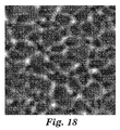
前述のように、現在説明しているマットフィルムはまた、フィルムの表面全域に不規則に配置されるミクロ構造を有するものとして理解してよい。かかる不規則化は、周期的構造から生じるモアレ干渉縞の発生を緩和するために重要である。表面の不規則性を測定するために役立つ1つの方法は、表面のフーリエスペクトル値を計算することである。フーリエスペクトルを測定し、不規則性の測定値を得る方法は、図18〜24を参照することによって理解できるであろう。図18は、本説明によるフィルムの地形図を示す。図形データ(即ち、高さ値)は、Matlabなど高機能の計算及び処理プログラムにインポートされてよい。ここからフーリエスペクトルを計算でき、図19に示すものなどの2次元スペクトルを作製できる。図27のスペクトルは、実際に下記に例示した実施例によるものである。次に2次元スペクトルによる線プロファイルは、図20に図示するように一連の方向で測定されてよい。スペクトルが対称であるために、スペクトルの半分だけを調べる必要がある。 As mentioned above, the currently described matte film may also be understood as having a microstructure that is randomly arranged across the surface of the film. Such irregularization is important for mitigating the occurrence of moire fringes resulting from periodic structures. One method that is useful for measuring surface irregularities is to calculate the Fourier spectral values of the surface. The method of measuring the Fourier spectrum and obtaining irregularity measurements can be understood by referring to FIGS. FIG. 18 shows a topographic map of the film according to the present description. Graphic data (ie, height values) may be imported into a sophisticated calculation and processing program such as Matlab. From here, a Fourier spectrum can be calculated, and a two-dimensional spectrum such as that shown in FIG. 19 can be produced. The spectrum of FIG. 27 is actually from the example illustrated below. A line profile with a two-dimensional spectrum may then be measured in a series of directions as illustrated in FIG. Because the spectrum is symmetric, only half of the spectrum needs to be examined.
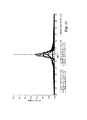
各線プロファイルの総信号が計算され、プロファイルの長さによって、場合によっては、図21に示すfx及びfy方向における不均等な周波数ステップによって正規化される。最大線プロファイル2110は、この正規化された和から選択される。次に、フーリエスペクトルの線プロファイル(最大信号方向)がプロットされる。このスペクトルにはメディアンフィルター処理が施されて、下記の工程におけるスパイク効果を除去する。図22にフーリエスペクトルを示す。メディアンフィルター処理が施されたスペクトルも示す。この時点では、ユーザーがスペクトル内のピークのすぐ左側にある最小値の地点又はその付近を選択し、極小値を見出す。図23に示すこの極小値2340からは、可視化を目的として一連の試験線分が極小値2340からスペクトルの下まで引かれ、各線分上の各点に対しては、スペクトルと試験線分との間の距離が計算され、50%の最接近点に対する距離の合計が計算される。これらの値は、探索線の長さによって正規化される。
The total signal for each line profile is calculated and normalized by the length of the profile and possibly by unequal frequency steps in the fx and fy directions shown in FIG. The
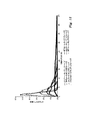
結果として生じた曲線の最小値は、スペクトルに最も接近する試験線に対応する。この線は、スペクトルの接線と見なされる。接線は、図24A及び24Bのグラフに適用される。探索は、スペクトルに最も接近する部分に対してこの接線に沿って実行される。この位置は、接線位置2420である。ピークの左側にある極小値及び接線位置は、ピークの境界を画定し、これらの間の線は基線を画定する。接線の下の領域(図24Bの斜線部分2430)に対するピークと接線との間の領域(図24Aの斜線部分2410)の比率は、地形の周期性の強さを指定するために用いられる。これらの領域は、線形(log10ではない)単位で計算される。本開示の目的のために、接線の下の領域に対するピークと接線との間の領域の比率は、RR1と呼ばれてよい。
The resulting minimum of the curve corresponds to the test line closest to the spectrum. This line is considered the tangent of the spectrum. Tangent lines apply to the graphs of FIGS. 24A and 24B. A search is performed along this tangent to the part closest to the spectrum. This position is a
本説明によるマットフィルムの多数の異なるRR1値のプロットを図25に示す。このグラフでは、RR1値は、所与のフィルムのヘイズ値に対して表示される。幾つかの実施形態では、RR1値は2未満である。幾つかの実施形態では、RR1値は1未満である。幾つかの実施形態では、RR1値は、更に0.5未満であってよい。これらの各値は、極めて不規則な配置(つまり、非周期アレイ)に相当すると理解できる。RR1値が低ければ、ミクロ構造アレイの周期性は低い。このグラフは、本明細書に開示された所与のヘイズ値を有する少なくとも幾つかのフィルムについて、周期性(又はその欠如)を示すために用いることができる。例えば、約20%未満、又は約10%未満、又は約7.5%未満、又は約5%未満、又は約3%未満、又は約1.5%未満のヘイズを有する本説明による所与のフィルムの場合、このフィルムは、2未満、又は1未満のRR1値を有してよい。 A plot of a number of different RR 1 values for a matte film according to this description is shown in FIG. In this graph, the RR 1 value is displayed for the haze value of a given film. In some embodiments, the RR 1 value is less than 2. In some embodiments, the RR 1 value is less than 1. In some embodiments, the RR 1 value may be further less than 0.5. Each of these values can be understood to correspond to a very irregular arrangement (ie an aperiodic array). If the RR 1 value is low, the periodicity of the microstructure array is low. This graph can be used to show periodicity (or lack thereof) for at least some films having a given haze value disclosed herein. For example, given a description according to the present description having a haze of less than about 20%, or less than about 10%, or less than about 7.5%, or less than about 5%, or less than about 3%, or less than about 1.5% In the case of a film, the film may have an RR 1 value of less than 2 or less than 1 .
多くの実施形態では、基材層170を含むことが有用であり得る。基材は、構造上の目的だけではなく、ミクロ構造化表面の作製及び成形プロセスにおいても有用であり得る。ミクロ構造化表面は、同一所有者による米国特許出願公開第2009/0029054号(参照によりその全体が本明細書に組み込まれる)に記載の方法に従って作製されてよい。したがって、基材170は、例えば、織布材料、編物材料、フィルム(例えば、高分子フィルム)、不織布、金属シート、金属箔、ガラスなどの可撓性材料を含む、基材として用いるのに好適な様々な材料のいずれかであってもよい。最終フィルム製品を光学ディスプレイなど光学用途で用いることが意図される幾つかの実施形態では、基材材料は、意図される用途に対して望ましい光学的特性及び機械的特性にある程度基づいて選択されるであろう。好適な光透過性光学フィルムの例としては、輝度向上多層光学フィルム(例えば、方向転換又は吸収)、偏光フィルム、拡散フィルム、及び補償フィルムが挙げられるが、これらに限定されない。機械的特性としては、可撓性、寸法安定性、及び衝撃耐性が挙げられてよい。幾つかの実施形態では、光学的に透明な材料(例えば、透明)が所望され得る。好適な光学的に透明な材料の例としては、光学的に透明なポリエステルフィルム、トリアセテート(TAC)フィルム、ポリエチレンナフタレート、ポリエチレンテレフタレート(PET)、ポリカーボネート、酢酸セルロース、ポリ(メチルメタクリレート)、二軸延伸ポリプロピレン(BOPP)及び同時二軸延伸ポリプロピレン(S−BOPP)などのポリオレフィン類などが挙げられる。基材170は、ポリアミド、ポリイミド、フェノール樹脂、ポリスチレン、スチレンーアクリロニトリルコポリマー、エポキシなどを含んでもよく、又はこれらからなってもよい。
In many embodiments, it may be useful to include a
前述のように、ミクロ構造化表面は、同一所有者による米国特許出願公開第2009/0029054号に記載の方法に従って作製されてよい。したがって、構造化表面は、基材上での初期コーティングで開始するプロセスによって形成されてよい。コーティングは、第1の粘度から第2の粘度へとその粘度を変化させる。粘度変化は、より液体様であり、コーティング可能である第1の粘度から、より固体様であり、したがって少なくとも一時的に構造を保持できる第2の粘度への移行と理解されてよい。粘度変化後、コーティングは、ミクロ構造化仕上げを付与する表面側ローラーと接触する。次にコーティングは、所望により硬化されてよい。したがって、用いられる基材は、硬化可能な基材であってよい。このプロセスは、図3を参照することにより、更に理解できるであろう。この実施形態によると、ミクロ構造化表面は、特定の所望の材料特性を有するであろう。この構造に従って作製されたミクロ構造化マットフィルムは、ロール誘導のマット光学構造体と呼ばれてよい。 As mentioned above, the microstructured surface may be made according to the method described in commonly owned US Patent Application Publication No. 2009/0029054. Thus, the structured surface may be formed by a process that begins with an initial coating on the substrate. The coating changes its viscosity from a first viscosity to a second viscosity. Viscosity change may be understood as a transition from a first viscosity that is more liquid-like and coatable to a second viscosity that is more solid-like and thus at least temporarily retains structure. After the viscosity change, the coating comes into contact with a surface side roller that imparts a microstructured finish. The coating may then be cured as desired. Thus, the substrate used may be a curable substrate. This process can be further understood with reference to FIG. According to this embodiment, the microstructured surface will have certain desired material properties. Microstructured matte films made according to this structure may be referred to as roll-derived matte optical structures.
フィルムを構造化するための装置は、図3に概略的に示す装置300として示される。図に示すように、少なくとも幾つかの実施形態では、コーティングは、コーティングアプリケータ312によって基材310に施される。通常、最初は液体状態であってよいコーティングの粘度は、濃化ステーション314で調整される。この粘度変化(第1の粘度から第2の粘度へ)は、樹脂溶液から揮発性溶媒を除去する、100%固体樹脂を冷却する、樹脂を部分架橋する、超高粘度樹脂を温める、これらの手法の2つ以上を組み合わせる、又は他の方法を使用することによって発生し得る。粘度変化後、コーティングされた層316には仕上げが施される。これは、一般にローラー、つまりニップである変換ステーション318で基材とコーティングを圧延することにより一般に達成できる。かかるニップの拡大図を図4に示す。ニップは、フィルム316を圧延する表面側ローラー340とバックアップロール350とを有する。コーティングされた基材の第1の主表面は、表面側ローラーと接触する。コーティング層の一部は、ニップで引き離され、残部がミクロ構造化表面を形成する。模様付きコーティング320は、固体に満たないことがあり得る状態で変換ステーションを離れる。したがって、図3に示すように、固化ステーション330を通って送達される。固化は、紫外線硬化、熱硬化、電子ビーム硬化、エポキシ硬化、更なる溶媒除去、又はその他を含む任意の数の好適な方法で実行されてよい。固化ステーション工程の結果、所定の位置322に固定された模様付きフィルムがもたらされる。
An apparatus for structuring the film is shown as
ある実施形態では、図3に示すプロセスにデコイニップが追加されてよい。かかる構造体を図5に示す。この実施形態では、フィルム510は、まずデコイニップ520を通過してから、変換ステーションニップ530に入る。この構造体は、大粒の埃粒子が変換ステーションニップに到達する状況において望ましいことがある。かかる状況では、デコイニップを追加することにより、構造化及び変換の前に埃を除去して収集できる。この場合においても、表面の構造は、固化ステーション540において所定の位置に固定される。
In some embodiments, a decoy nip may be added to the process shown in FIG. Such a structure is shown in FIG. In this embodiment, the
デコイニップは、前述のように、欠陥をもたらす埃などのくずや粒子を収集して除去するために用いられる。この装置は、低清浄度環境における構造化プロセスのロバスト性を向上するために有用である。デコイニップは、変換ステーションニップと同等以上の微粒子に対する親和性を有する。デコイニップは、作製される最終構造化コーティングに悪影響を及ぼすことなく、除去しなければ変換ステーションニップ上で捕捉されるであろうくずを液体コーティングから除去する。デコイロールニップから変換ステーションロールニップまでの距離は、製造環境の清浄度に応じて異なってよい。 As described above, the decoy nip is used to collect and remove dust such as dust and particles that cause defects. This device is useful for improving the robustness of the structured process in a low cleanliness environment. The decoy nip has an affinity for fine particles equal to or better than the conversion station nip. The decoy nip removes debris from the liquid coating that would otherwise be trapped on the conversion station nip without adversely affecting the final structured coating that is made. The distance from the decoy roll nip to the conversion station roll nip may vary depending on the cleanliness of the manufacturing environment.
本説明で用いるのに好適なコーティング可能な材料は、様々なフィルム形成材料のいずれかを含んでよい。幾つかの実施形態では、コーティング可能な材料は、溶媒中の1つ以上のポリマー及び/又はオリゴマーを含むポリマー材料である。幾つかの実施形態では、コーティング可能な材料は、1つ以上の溶媒中の1つ以上のモノマー、オリゴマー、及び/又はポリマーの混合物である。他の実施形態では、コーティング可能な材料は、大量の粒子又はナノ粒子と共に、1つ以上の溶媒中の前述のオリゴマー、モノマー、及び/又はポリマーを含む。ある実施形態では、コーティング可能な材料は、光開始剤、架橋剤、静電気防止化合物、及び他の活性物質を含んでよい。 Suitable coatable materials for use in the present description may include any of a variety of film forming materials. In some embodiments, the coatable material is a polymeric material comprising one or more polymers and / or oligomers in a solvent. In some embodiments, the coatable material is a mixture of one or more monomers, oligomers, and / or polymers in one or more solvents. In other embodiments, the coatable material comprises the aforementioned oligomers, monomers, and / or polymers in one or more solvents, along with bulk particles or nanoparticles. In certain embodiments, the coatable material may include a photoinitiator, a crosslinker, an antistatic compound, and other active materials.
ナノ粒子を表面改質できるが、これはナノ粒子が改質された表面を有し、例えば、ナノ粒子が安定な分散体を提供することを指す。「安定な分散体」は、例えば、室温(約20〜22℃)及び大気圧、過剰な電磁力がないという周囲条件下で、一定の時間、例えば、約24時間放置された後に、コロイド状ナノ粒子が粒塊しない分散体を指す。 Nanoparticles can be surface modified, which means that the nanoparticles have a modified surface, eg, the nanoparticles provide a stable dispersion. A “stable dispersion” is, for example, colloidal after standing at room temperature (about 20-22 ° C.) and atmospheric pressure, ambient conditions without excess electromagnetic force, for a period of time, for example about 24 hours. A dispersion in which nanoparticles do not agglomerate.
表面改質されたコロイド状ナノ粒子は、任意に、本明細書のコーティング可能な組成物として用いられるポリマーコーティング中に、最終要素、つまり光学要素の耐久性を高めるのに有効な量で存在するナノ粒子と共に存在してよい。本明細書に記載される表面改質されたコロイド状ナノ粒子は、例えば、ナノ粒子がコーティング可能な組成物内で安定な分散体を形成するようにする、ナノ粒子のコーティング可能な組成物との相溶性、より耐久性のある複合物にする、ナノ粒子のコーティング可能な組成物との反応性、及び低影響性又は未硬化組成物の粘性など様々な好ましい特質を有することができる。表面改質の組み合わせを利用して、組成物の未硬化及び硬化特性を操作できる。表面改質されたナノ粒子は、コーティング可能な組成物の光学的及び物理的特性を改善でき、これは例えば、樹脂の機械的強度の改善、コーティング可能な組成物中に負荷される固体量増加の間の粘度変化の最小化、及び、コーティング可能な組成物中に負荷される固体量増加の間の光学的透明度の維持などである。 The surface-modified colloidal nanoparticles are optionally present in an amount effective to enhance the durability of the final element, i.e., the optical element, in the polymer coating used as the coatable composition herein. It may be present with the nanoparticles. The surface-modified colloidal nanoparticles described herein include a nanoparticle coatable composition, for example, such that the nanoparticles form a stable dispersion within the coatable composition. Can have various favorable attributes such as compatibility of the nanoparticles, reactivity of the nanoparticles with the coatable composition, and low impact or viscosity of the uncured composition. A combination of surface modification can be utilized to manipulate the uncured and cured properties of the composition. Surface-modified nanoparticles can improve the optical and physical properties of the coatable composition, such as improving the mechanical strength of the resin, increasing the amount of solids loaded in the coatable composition Such as minimizing changes in viscosity during maintenance and maintaining optical clarity while increasing the amount of solids loaded into the coatable composition.
幾つかの実施形態において、ナノ粒子は表面改質されたナノ粒子である。好適な表面改質されたコロイド状ナノ粒子は、オキシド粒子を含んでよい。ナノ粒子は、所与の材料について周知の粒径分布にわたる粒径範囲を含んでよい。幾つかの実施形態において、平均粒子サイズは約1nm〜約100nmの範囲内であってよい。粒径及び粒径分布は、例えば、透過電子顕微鏡(TEM)などによる周知の方法で測定できる。好適なナノ粒子は、任意の様々な物質、例えば、アルミナ、酸化スズ、酸化アンチモン、シリカ、ジルコニア、チタニア、及びこれらのうちの2つ以上の組み合わせから選択される金属酸化物を含んでよい。表面改質されたコロイド状ナノ粒子は、実質的に完全に凝縮され得る。 In some embodiments, the nanoparticles are surface modified nanoparticles. Suitable surface modified colloidal nanoparticles may include oxide particles. Nanoparticles may include a range of particle sizes over a known particle size distribution for a given material. In some embodiments, the average particle size may be in the range of about 1 nm to about 100 nm. The particle size and particle size distribution can be measured by a well-known method using, for example, a transmission electron microscope (TEM). Suitable nanoparticles may comprise a metal oxide selected from any of a variety of materials, such as alumina, tin oxide, antimony oxide, silica, zirconia, titania, and combinations of two or more thereof. The surface modified colloidal nanoparticles can be substantially completely condensed.
幾つかの実施形態において、シリカナノ粒子は、約5〜約75nmの範囲の粒径を有することができる。幾つかの実施形態において、シリカナノ粒子は、約10〜約30nmの範囲の粒径を有することができる。シリカナノ粒子は、約10〜約100phrの量でコーティング可能な組成物中に存在してよい。幾つかの実施形態では、シリカナノ粒子は、約25〜約80phrの量でコーティング可能な組成物中に存在し、他の実施形態では、シリカナノ粒子は、約30〜約70phrの量でコーティング可能な組成物中に存在してよい。本説明のコーティング可能な組成物で用いるのに好適なシリカナノ粒子は、Nalco Chemical Co.(Naperville,Ill.)から製品名NALCO COLLOIDAL SILICASで市販される。好適なシリカ製品として、NALCO製品1040、1042、1050、1060、2327及び2329が挙げられる。好適なヒュームドシリカ製品として、例えば、DeGussa AG(Hanau,Germany)から商品名AEROSILシリーズOX−50、−130、−150、及び−200として、並びにCabot Corp.(Tuscola,Ill.)からCAB−O−SPERSE 2095、CAB−O−SPERSE A105、及びCAB−O−SIL MSとして販売される製品が挙げられる。ナノ粒子の表面処理は、コーティング可能な組成物(例えば、ポリマー樹脂)中で安定な分散体を提供できる。好ましくは、粒子がコーティング可能な組成物中に良好に分散されて、実質的に均一な組成物を生じるように、ナノ粒子を表面処理により安定化させる。更に、ナノ粒子は、安定化させた粒子が硬化中にコーティング可能な組成物と共重合又は反応できるように、その表面の少なくとも一部を表面処理剤により改質し得る。 In some embodiments, the silica nanoparticles can have a particle size in the range of about 5 to about 75 nm. In some embodiments, the silica nanoparticles can have a particle size in the range of about 10 to about 30 nm. Silica nanoparticles may be present in the coatable composition in an amount of about 10 to about 100 phr. In some embodiments, the silica nanoparticles are present in the coatable composition in an amount of about 25 to about 80 phr, and in other embodiments, the silica nanoparticles can be coated in an amount of about 30 to about 70 phr. It may be present in the composition. Silica nanoparticles suitable for use in the coatable compositions of the present description include Nalco Chemical Co. (Naperville, Ill.) Under the product name NALCO COLORIDAL SILICAS. Suitable silica products include NALCO products 1040, 1042, 1050, 1060, 2327 and 2329. Suitable fumed silica products are available, for example, from DeGussa AG (Hanau, Germany) under the trade names AEROSIL series OX-50, -130, -150, and -200, and Cabot Corp. (Tuscola, Ill.) Include products sold as CAB-O-SPERSE 2095, CAB-O-SPERSE A105, and CAB-O-SIL MS. Surface treatment of the nanoparticles can provide a stable dispersion in a coatable composition (eg, a polymer resin). Preferably, the nanoparticles are stabilized by a surface treatment so that the particles are well dispersed in the coatable composition, resulting in a substantially uniform composition. In addition, the nanoparticles can be modified with at least a portion of their surface with a surface treatment so that the stabilized particles can be copolymerized or reacted with the coatable composition during curing.
多数のマットフィルムは、ミクロ構造の主たる形成理由として粒子が機能するように十分に大粒の粒子を含む。かかるフィルムを図6に示す。かかる実施形態では、光学フィルム800は、ミクロ構造化層860に機械的に結合された基材、つまり第1のフィルム850を有する。この実施形態では、粒子830は結合剤840中に分散している。粒子830の寸法は、規模の面においてミクロ構造870の実際の幅又は高さに非常に近い。現在の説明は、粒子を有する構造化表面160を提供する。しかし、現在の説明の粒子は、コーティング層の厚さに対して小さいため、ミクロ構造の主たる形成理由として機能しない。マットコーティングのヘイズ、透明度、透過率などの光学特性は、コーティング厚、並びにかかる粒子の密度及び分布に対する粒子の寸法によってある程度制御される。現在の説明に従って設計されたフィルムの例を図7に示す。ここでは、光学フィルム、つまりフィルム積層体900は、ミクロ構造化層960に機械的に結合された基材層、つまり第1のフィルム950を有する。粒子930は結合剤940中に分散している。全ての位置における層厚、特にミクロ構造970のピークにおける層厚は、粒子930の厚さよりも著しく大きいことは容易に明らかである。具体的には、光学フィルム中の粒子は、0.5マイクロメートル未満の寸法、幾つかの実施形態では、0.2マイクロメートル未満、又は0.1マイクロメートル未満の寸法を有する。
Many matte films contain sufficiently large particles so that the particles function as the primary reason for forming the microstructure. Such a film is shown in FIG. In such an embodiment, the
幾つかの実施形態では、構造化表面は、約1.50〜1.70の屈折率を有するであろう。他の実施形態では、構造化表面は、約1.17のように低い屈折率から約1.8のように高い屈折率までを有してよい。 In some embodiments, the structured surface will have a refractive index of about 1.50 to 1.70. In other embodiments, the structured surface may have a low refractive index, such as about 1.17, to a high refractive index, such as about 1.8.
ヘイズ及び透明度の性能は、図8及び9を参照することにより、更に理解できるであろう。図8は、本説明に従って作製された多数のフィルムの全てのヘイズ及び透明度のスペクトルを示す。他の構造化フィルムに対する性能上の利点を示すために、他の13の構造化フィルムと比較して示す。フィルム1は、3M製のビードコーティングされたマットフィルムである。フィルム2は、PET上に白色インクで模様が付けられたフィルムである。フィルム3は、Keiwa 100−BMUISフィルムである。フィルム4は、ビードコーティングされたマットフィルムである。フィルム5は、粒子ビードコーティングされたマットフィルムである。フィルム6は、Kimoto 100TL4フィルムである。フィルム7は、フィルムの表面にフレームエンボス加工を施して作製されたマットフィルムである。フィルム8は、電着を使用して作製されたミクロ複製マットフィルムである。フィルム9は、押出可能な剥離性膜の貼り付け及び除去により非平滑化されたフィルムである。フィルム10は、ミクロ複製されたマットフィルムである。フィルム11は、グラビアコーティング中に分散したビードを含むマットフィルムである。フィルム12は、ミクロ複製された、機械加工マットフィルムである。フィルム13は、Dai Nippon DNP M268Yフィルムである。図8及び9を参照すれば明確に理解できるように、現在の説明によるフィルムの多くは、非常に低いヘイズ値及び非常に高い透明度値を示す。図9は、この性能を最も良く理解するために参照され得る。この図は、計測された0〜20%のヘイズ率及び0〜100%の透明度範囲を示す。
The haze and transparency performance can be further understood with reference to FIGS. FIG. 8 shows all the haze and transparency spectra of a number of films made according to this description. To show the performance advantages over other structured films, it is shown in comparison with the other 13 structured films. The
図9は、現在の説明が、他のフィルムでは達しないレベルの性能に達することを明確に示す。例えば、一態様では、このフィルムは、50%未満の光学的透明度値及び10%未満の光学的ヘイズ値を有するものとして理解されてよい。別の態様では、本説明のフィルムは、約7.5%未満の光学的ヘイズ及び約60%の光学的透明度を有するものとして理解されてよい。この性能範囲内には、1つ又は2つの他のフィルム(例えば、3M Particle Matte)が該当してよい。しかし、かかるフィルムは全て、現在のフィルムが約0.5マイクロメートル未満、又は約0.2マイクロメートル未満の粒径を含む構造化表面を備え、この性能を示す点において区別できる。別の態様では、本説明のフィルムは、約5%未満の光学的ヘイズ及び約70%未満の光学的透明度を有するものとして理解されてよく、この場合においても、このフィルムの構造化表面は約0.5マイクロメートル未満、又は約0.2マイクロメートル未満の寸法の粒子で構成される。 FIG. 9 clearly shows that the current description reaches a level of performance not reached with other films. For example, in one aspect, the film may be understood as having an optical clarity value of less than 50% and an optical haze value of less than 10%. In another aspect, the films described herein may be understood as having an optical haze of less than about 7.5% and an optical clarity of about 60%. Within this performance range, one or two other films (eg, 3M Particle Matte) may be applicable. However, all such films are distinguishable in that current films have a structured surface comprising a particle size of less than about 0.5 micrometers, or less than about 0.2 micrometers, and exhibit this performance. In another aspect, the described film may be understood as having an optical haze of less than about 5% and an optical clarity of less than about 70%, and in this case the structured surface of the film is about Consists of particles with dimensions of less than 0.5 micrometers, or less than about 0.2 micrometers.
更に別の実施形態では、図8において、及び図9においてより明確に示されるように、本説明のフィルムは、約3%未満の光学的ヘイズ及び約65%未満又は75%未満の光学的透明度を有する。更に別の態様では、フィルムは、約1.5%未満の光学的ヘイズ及び約80%未満の光学的透明度を有するものとして理解されてよい。更に別の態様では、フィルムは、約1%未満の光学的ヘイズ及び約90%未満の光学的透明度を有するものとして理解されてよい。また、現在のフィルムは、約20%未満の光学的ヘイズ及び約40%未満の光学的透明度を有するものとして理解されてよい。 In yet another embodiment, as shown more clearly in FIG. 8 and in FIG. 9, the films described herein have an optical haze of less than about 3% and an optical clarity of less than about 65% or less than 75%. Have In yet another aspect, the film may be understood as having an optical haze of less than about 1.5% and an optical clarity of less than about 80%. In yet another aspect, the film may be understood as having an optical haze of less than about 1% and an optical clarity of less than about 90%. Current films may also be understood as having an optical haze of less than about 20% and an optical clarity of less than about 40%.
別の様式では、本説明のフィルムは、約75%〜95%の光学的透明度及び約0〜1%の光学的ヘイズを有するものとして理解されてよく、このフィルムは、約0.5マイクロメートル未満の平均寸法の粒子で構成される。また、このフィルムは、約35%〜70%の光学的透明度及び約1〜4%の光学的ヘイズを有してよい。また、このフィルムは、約30%〜55%の光学的透明度及び約4〜10%の光学的ヘイズを有してよく、このフィルムは、約0.5マイクロメートル未満の平均寸法の粒子で構成される。別の実施形態では、このフィルムは、この場合においても約0.5マイクロメートル未満の平均寸法の粒子で構成され、このフィルムの光学的透明度値は約25%〜45%であり、光学的ヘイズ値は約10%〜18%である。 Alternatively, the described film may be understood as having an optical clarity of about 75% to 95% and an optical haze of about 0 to 1%, the film having a thickness of about 0.5 micrometers. Composed of particles of less than average size. The film may also have an optical clarity of about 35% to 70% and an optical haze of about 1-4%. The film may also have an optical clarity of about 30% to 55% and an optical haze of about 4 to 10%, the film being composed of particles having an average size of less than about 0.5 micrometers. Is done. In another embodiment, the film is again composed of particles with an average size of less than about 0.5 micrometers, the optical clarity value of the film is about 25% to 45%, and the optical haze The value is about 10% to 18%.
構造化表面が第2のフィルムとして説明され、基材が第1のフィルムとして説明される更に別の態様では、第2のフィルムは、約85%未満の光学的透明度及び約3.5%未満の光学的ヘイズを有する。 In yet another embodiment where the structured surface is described as a second film and the substrate is described as a first film, the second film is less than about 85% optical clarity and less than about 3.5%. It has an optical haze of
図10は、マット層140の一部の概略的側面図である。詳細には、図10は、構造化表面120におけるミクロ構造160を示す。ミクロ構造160は、ミクロ構造の表面全域に勾配分布を有する。例えば、ミクロ構造は、位置510において勾配θを有し、θは、位置510においてミクロ構造面に垂直である(α=90度)法線520と、同一の位置でミクロ構造面に接する接線530との間の角度である。傾きθは、接線530と艶消し層の主面142との間の角度でもある。
FIG. 10 is a schematic side view of a portion of the
ミクロ構造の勾配を最も良く理解するために、構造化表面120の勾配は、まずx方向に沿って測定し、次にy方向に沿って測定した。即ち、次のとおりである。
In order to best understand the gradient of the microstructure, the gradient of the

平均x勾配及びy勾配は、各ピクセルに中心がある6マイクロメートルの間隔で評価した。別の実施形態では、一定間隔を用いる限り、このマイクロメートルの間隔は、2マイクロメートル、又は3マイクロメートルなどより小さくなるように選択してよい。x勾配及びy勾配のデータから、勾配規模を決定することが可能である。これは、次のように理解できる。 Average x and y gradients were evaluated at 6 micron intervals centered on each pixel. In another embodiment, as long as a constant spacing is used, the micrometer spacing may be selected to be smaller than 2 micrometers, 3 micrometers, or the like. From the x and y gradient data, it is possible to determine the gradient magnitude. This can be understood as follows.
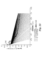
本説明の多数の実施形態についてX勾配分布及びY勾配分布を計算した。これらのフィルムは、0.7%、1.2%、1.6%、8%、23%、40%、及び80%のヘイズ値を有した。図11は、本説明に従って作製されたこれら7つのフィルムのx勾配分布を示す。図12は、同じ7つのフィルムのy勾配分布を示す。2つのグラフから容易に明らかなように、フィルムの表面の大部分は、x及びyの両方向において非常に小さい勾配を有する。最低ヘイズ値(1.6%以下)を有したフィルムはまた、x勾配分布及びy勾配分の両方において0度勾配に相当する領域の最高の正規化カウントを有した。同様のデータからは、本説明に従って作製された7つの異なるフィルムについて、上記の等式から勾配規模分布を生成することが可能であった。図13は、この勾配規模分布を示す。このグラフにおいても、非常に低い勾配を有する各フィルムが多量の表面を有することが示される。最も高い3つのピークは、1.6%ヘイズ、1.2%ヘイズ、及び0.7%ヘイズのヘイズ値に対するものであった。このデータは、対応する相補累積勾配分布(FCC(θ))によって更に理解できるであろう。図14にFCCグラフを示す。これから、フィルムの所与のヘイズ値に準じて表面の様々な勾配を決定することが可能であった。したがって、所与の数未満の勾配を有するフィルムの表面の割合は、フィルムの様々なヘイズ値に準じて数値化されてよい。 X gradient distribution and Y gradient distribution were calculated for a number of embodiments of the present description. These films had haze values of 0.7%, 1.2%, 1.6%, 8%, 23%, 40%, and 80%. FIG. 11 shows the x-gradient distribution of these seven films made according to this description. FIG. 12 shows the y-gradient distribution of the same seven films. As is readily apparent from the two graphs, the majority of the film surface has a very small slope in both the x and y directions. The film with the lowest haze value (below 1.6%) also had the highest normalized count of the area corresponding to a 0 degree gradient in both the x-gradient distribution and the y-gradient. From similar data, it was possible to generate a gradient magnitude distribution from the above equation for seven different films made according to this description. FIG. 13 shows this gradient magnitude distribution. This graph also shows that each film with a very low slope has a large amount of surface. The three highest peaks were for haze values of 1.6% haze, 1.2% haze, and 0.7% haze. This data can be further understood by the corresponding complementary cumulative gradient distribution (F CC (θ)). FIG. 14 shows an FCC graph. From this it was possible to determine various surface gradients according to the given haze value of the film. Thus, the percentage of the surface of a film that has a gradient less than a given number may be quantified according to the various haze values of the film.
この理解によると、フィルムの表面勾配は、ヘイズ値と相関性があると理解されてよい。したがって、約10%未満のヘイズ値を有するフィルムの場合、このフィルムの構造化表面の少なくとも85%は、約7.5度未満である勾配規模を有してよい。他のフィルムでは、構造化表面の95%は、約10度未満である勾配規模を有する。更に、構造化表面の95%は、約5度未満である勾配規模を有してよい。 According to this understanding, the surface gradient of the film may be understood to correlate with the haze value. Thus, for a film having a haze value of less than about 10%, at least 85% of the structured surface of the film may have a gradient magnitude that is less than about 7.5 degrees. In other films, 95% of the structured surface has a gradient magnitude that is less than about 10 degrees. Further, 95% of the structured surface may have a gradient magnitude that is less than about 5 degrees.
フィルムのヘイズ値が約7.5%未満である場合、構造化表面の90%は、約7.5度未満である勾配規模を有してよい。この同一のヘイズ値を有するフィルムでは、構造化表面の97%は、約10度未満である勾配規模を有してよい。更に、構造化表面の95%は、約5度未満である勾配規模を有してよい。 If the haze value of the film is less than about 7.5%, 90% of the structured surface may have a gradient magnitude that is less than about 7.5 degrees. In films having this same haze value, 97% of the structured surface may have a gradient magnitude that is less than about 10 degrees. Further, 95% of the structured surface may have a gradient magnitude that is less than about 5 degrees.
フィルムのヘイズ値が約5%未満である場合、構造化表面の85%は、約5度未満である勾配規模を有してよい。この同一のヘイズ値を有するフィルムでは、構造化表面の90%は、約5度未満、又は約4度未満である勾配を有してよい。 If the haze value of the film is less than about 5%, 85% of the structured surface may have a gradient magnitude that is less than about 5 degrees. In films having this same haze value, 90% of the structured surface may have a slope that is less than about 5 degrees, or less than about 4 degrees.
フィルムのヘイズ値が約3%未満である本説明の別の態様では、構造化表面の少なくとも90%は約5度未満の勾配規模を有してよいか、少なくとも95%の構造化表面は約5度未満である勾配規模を有してよい。 In another aspect of the present description where the haze value of the film is less than about 3%, at least 90% of the structured surface may have a gradient magnitude of less than about 5 degrees, or at least 95% of the structured surface is about It may have a gradient magnitude that is less than 5 degrees.
フィルムのヘイズ値が約1.5%未満である場合、構造化表面の少なくとも80%は、約2.5度未満である勾配規模を有してよい。この同一のヘイズ値を有するフィルムでは、構造化表面の少なくとも98%は、約5度未満である勾配規模を有してよい。 If the haze value of the film is less than about 1.5%, at least 80% of the structured surface may have a gradient magnitude that is less than about 2.5 degrees. In films having this same haze value, at least 98% of the structured surface may have a gradient magnitude that is less than about 5 degrees.
フィルムの光学的ヘイズ値が約1%未満である場合、構造化表面の少なくとも90%は約4度未満である勾配規模を有してよいか、構造化表面の99%は約5度未満である勾配規模を有してよい。 If the optical haze value of the film is less than about 1%, at least 90% of the structured surface may have a gradient magnitude that is less than about 4 degrees, or 99% of the structured surface is less than about 5 degrees. It may have a certain gradient magnitude.
光学的ヘイズが約20%未満である実施形態では、構造化表面の少なくとも90%は、約7度未満、又は約10度未満である勾配規模を有してよい。 In embodiments where the optical haze is less than about 20%, at least 90% of the structured surface may have a gradient magnitude that is less than about 7 degrees, or less than about 10 degrees.
別の態様では、光学フィルムの少なくとも50%は、約1度〜5度の勾配を有するものとして理解されてよい。 In another aspect, at least 50% of the optical film may be understood as having a gradient of about 1 to 5 degrees.
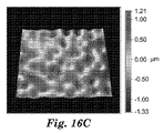
図16A及び16Cは、本説明による特定のフィルムの、xプロファイル及びyプロファイルに沿った原子間力顕微鏡の画像を示す。図16Cは、フィルムの対応するXプロファイルを示し、16Dは、フィルムの対応するYプロファイルを示す。図に示される特定のフィルムは、0.7%の光学的ヘイズ及び70.9%の光学的透明度を有した。Xプロファイル(図16B)及びYプロファイル(図16D)に示されるフィルムの不規則な分布と不規則な高さの変化に気付くであろう。更に、プロファイルグラフは大きい勾配を有するように見えることがあるが、x軸及びy軸の目盛が極めて不釣り合いである。Yプロファイルの最も急な勾配は、約300μm〜350μmの横方向範囲にわたって約+0.35μmの高さレベルから−0.95μmまで移動した。これは、わずか−.026の負勾配に等しく、更にフィルムの平面からの小角度に等しい。y/xは、勾配及び勾配角の接線の両方に等しいため、逆正接(.026)は角度をもたらす。より具体的には、逆正接(.026)は、角度1.49度をもたらす。 16A and 16C show atomic force microscope images along the x and y profiles of a particular film according to the present description. FIG. 16C shows the corresponding X profile of the film, and 16D shows the corresponding Y profile of the film. The particular film shown in the figure had an optical haze of 0.7% and an optical clarity of 70.9%. You will notice irregular distribution and irregular height variations of the film shown in the X profile (FIG. 16B) and Y profile (FIG. 16D). Furthermore, the profile graph may appear to have a large slope, but the x-axis and y-axis scales are very disproportionate. The steepest slope of the Y profile moved from a height level of about +0.35 μm to −0.95 μm over a lateral range of about 300 μm to 350 μm. This is a slight-. Equivalent to a negative slope of 026 and equal to a small angle from the plane of the film. Since y / x is equal to both the slope and the tangent of the slope angle, the arc tangent (.026) yields an angle. More specifically, the arc tangent (.026) results in an angle of 1.49 degrees.
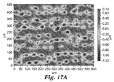
図17A及び17Cは、現在の説明による所与のフィルムの別の画像を示す。この画像では、フィルムのWyko位相シフト干渉計の画像をxプロファイル及びyプロファイルに沿って撮影した。このフィルムは、1.4%の光学的ヘイズ値及び69.6%の光学的透明度値を有した。示されるxプロファイル(図17Bに示す)及びyプロファイル(図17Dに示す)はより急激な勾配を示すように見えるが、この場合もまた、x方向における30μmの横方向移動(270から300μmへ)により1.5μm(−1.0から+0.5へ)のz変化が生じるなど(図17Bを参照)、軸の目盛が不釣り合いであった。ほぼ同一規模の垂直偏差がyプロファイルでも見られた。上記のxプロファイルの計算は、0.05の勾配を示した。これは、2.86度の角度(ここでも逆正接から計算した)に等しい。 17A and 17C show another image of a given film according to the current description. In this image, a Wyko phase shift interferometer image of the film was taken along the x and y profiles. This film had an optical haze value of 1.4% and an optical clarity value of 69.6%. The x profile shown (shown in FIG. 17B) and y profile (shown in FIG. 17D) appear to show a steeper slope, but again, 30 μm lateral movement in the x direction (from 270 to 300 μm) Caused a z change of 1.5 μm (from −1.0 to +0.5) (see FIG. 17B), and the scale of the shaft was unbalanced. Nearly the same vertical deviation was seen in the y profile. The above x-profile calculation showed a slope of 0.05. This is equal to an angle of 2.86 degrees (again calculated from the arc tangent).
別のサンプルは、本説明に従って作製されたフィルムの測定値であった。表面の走査型電子顕微鏡の画像を図26に示す。このサンプルは、2.47%のヘイズ値及び59.1%の光学的透明度値を有することが測定された。上記のフーリエ計算法に従って、フィルムプロファイルのフーリエスペクトルを作製した。このサンプルのスペクトルを図27に示す。このスペクトルからは、上記に開示し、図18〜24A及びBに示す方法にここでも従って、図28に示すようにこのサンプルのピークプロファイルを作製した。これから、このフィルムプロファイルのフーリエ比RR1値が0.65であったことを測定することが可能であった。 Another sample was a measurement of a film made according to this description. An image of the surface scanning electron microscope is shown in FIG. This sample was measured to have a haze value of 2.47% and an optical clarity value of 59.1%. A Fourier spectrum of the film profile was prepared according to the above Fourier calculation method. The spectrum of this sample is shown in FIG. From this spectrum, the peak profile of this sample was generated as shown in FIG. 28, again following the method disclosed above and shown in FIGS. 18-24A and B. From this, it was possible to measure that the Fourier ratio RR 1 value of this film profile was 0.65.
項目1.
約10%未満の光学的ヘイズと、
約50%未満の光学的透明度と、を有する構造化表面を備え、
構造化表面の少なくとも85%が約7.5度未満である勾配規模を有する、光学フィルム。
Less than about 10% optical haze;
Having a structured surface having an optical clarity of less than about 50%;
An optical film having a gradient scale in which at least 85% of the structured surface is less than about 7.5 degrees.
項目2.構造化表面上の構造が約10μm未満の平均高さを有する、項目1の光学フィルム。
項目3.構造化表面が硬化可能な基材を含む、項目1の光学フィルム。
項目4.構造化表面が約1.50〜1.70の屈折率を有する、項目1の光学フィルム。
項目5.光学フィルムが、約0.5マイクロメートル未満である平均寸法を有する複数の粒子を更に含む、項目1の光学フィルム。
項目6.光学フィルムが、約0.2マイクロメートル未満である平均寸法を有する複数の粒子を更に含む、項目5の光学フィルム。
項目7.光学フィルムが、約0.1マイクロメートル未満である平均寸法を有する複数の粒子を更に含む、項目6の光学フィルム。
項目8.粒子が表面改質されている、項目7の光学フィルム。
項目9.構造化表面の光学的透明度が約45%未満である、項目1の光学フィルム。
Item 9. The optical film of
項目10.構造化表面の少なくとも95%が約10度未満である勾配規模を有する、項目1の光学フィルム。
項目11.構造化表面の少なくとも95%が約5度未満である勾配規模を有する、項目5の光学フィルム。
Item 11. 6. The optical film of
項目12.フィルムが2未満のRR1値を有するように構造化表面上の構造が分布している、項目1の光学フィルム。
項目13.フィルムが1未満のRR1値を有するように構造化表面上の構造が分布している、項目12の光学フィルム。
項目14.更に基材を含み、基材上に構造化表面が配置され、構造化表面及び基材がそれぞれ屈折率を有する、項目1の光学フィルム。
項目15.構造化表面の屈折率が基材の屈折率よりも小さい、項目14の光学フィルム。
項目16.
約7.5%未満の光学的ヘイズと、
約60%未満の光学的透明度と、を有する構造化表面を備え、
構造化表面の少なくとも90%が約7.5度未満である勾配規模を有し、
約0.5マイクロメートル未満である平均寸法を有する複数の粒子を含む、光学フィルム。
Less than about 7.5% optical haze;
Having a structured surface having an optical clarity of less than about 60%;
At least 90% of the structured surface has a gradient magnitude that is less than about 7.5 degrees;
An optical film comprising a plurality of particles having an average dimension that is less than about 0.5 micrometers.
項目17.複数の粒子が約0.2マイクロメートル未満である平均寸法を有する、項目16の光学フィルム。
項目18.光学フィルムが、約0.1マイクロメートル未満である平均寸法を有する複数の粒子を更に含む、項目17の光学フィルム。
項目19.粒子が表面改質されている、項目18の光学フィルム。
項目20.構造化表面上の構造が約7.5μm未満の平均高さを有する、項目16の光学フィルム。
項目21.構造化表面の少なくとも97%が約10度未満である勾配規模を有する、項目16の光学フィルム。
Item 21.
項目22.構造化表面の少なくとも95%が約5度未満の勾配規模を有する、項目16の光学フィルム。
Item 22. The optical film of
項目23.構造化表面の光学的透明度が約55%未満である、項目16の光学フィルム。
項目24.フィルムが2未満のRR1値を有するように構造化表面上の構造が分布している、項目16の光学フィルム。
Item 24. 17. The optical film of
項目25.フィルムが1未満のRR1値を有するように構造化表面上の構造が分布している、項目24の光学フィルム。
項目26.更に基材を含み、基材上に構造化表面が配置され、構造化表面及び基材がそれぞれ屈折率を有する、項目16の光学フィルム。
Item 26.
項目27.構造化表面の屈折率が基材の屈折率よりも小さい、項目26の光学フィルム。 Item 27. 27. The optical film of item 26, wherein the refractive index of the structured surface is less than the refractive index of the substrate.
項目28.構造化表面が約1.50〜1.70の屈折率を有する、項目26の光学フィルム。 Item 28. 27. The optical film of item 26, wherein the structured surface has a refractive index of about 1.50 to 1.70.
項目29.
約5%未満の光学的ヘイズと、
約70%未満の光学的透明度と、を有する構造化表面を備え、
構造化表面の少なくとも85%のが約5度未満の勾配規模を有し、
約0.5マイクロメートル未満の平均寸法を有する複数の粒子を含む、光学フィルム。
Item 29.
Less than about 5% optical haze;
Having a structured surface having an optical clarity of less than about 70%;
At least 85% of the structured surface has a gradient magnitude of less than about 5 degrees;
An optical film comprising a plurality of particles having an average dimension of less than about 0.5 micrometers.
項目30.複数の粒子が約0.2マイクロメートル未満である平均寸法を有する、項目29の光学フィルム。
項目31.光学フィルムが、約0.1マイクロメートル未満である平均寸法を有する複数の粒子を更に含む、項目30の光学フィルム。
Item 31. 30. The optical film of
項目32.粒子が表面改質されている、項目31の光学フィルム。 Item 32. Item 31. The optical film of item 31, wherein the particles are surface modified.
項目33.構造化表面上の構造が約5μm未満の平均高さを有する、項目29の光学フィルム。 Item 33. 30. The optical film of item 29, wherein the structure on the structured surface has an average height of less than about 5 μm.
項目34.構造化表面の光学的透明度が約60%未満である、項目29の光学フィルム。 Item 34. 30. The optical film of item 29, wherein the structured surface has an optical clarity of less than about 60%.
項目35.構造化表面の少なくとも90%が約4度未満である勾配を有する、項目29の光学フィルム。
項目36.構造化表面の少なくとも90%が約5度未満である勾配規模を有する、項目29の光学フィルム。 Item 36. 30. The optical film of item 29, wherein at least 90% of the structured surface has a gradient magnitude that is less than about 5 degrees.
項目37.フィルムが2未満のRR1値を有するように構造化表面上の構造が分布している、項目29の光学フィルム。 Item 37. 30. The optical film of item 29, wherein the structure on the structured surface is distributed such that the film has an RR 1 value of less than 2.
項目38.フィルムが1未満のRR1値を有するように構造化表面上の構造が分布している、項目37の光学フィルム。 Item 38. 38. The optical film of item 37, wherein the structure on the structured surface is distributed such that the film has an RR 1 value of less than 1 .
項目39.更に基材を含み、基材上に構造化表面が配置され、構造化表面及び基材がそれぞれ屈折率を有する、項目29の光学フィルム。 Item 39. 30. The optical film of item 29, further comprising a substrate, wherein the structured surface is disposed on the substrate, the structured surface and the substrate each having a refractive index.
項目40.構造化表面の屈折率が基材の屈折率よりも小さい、項目39の光学フィルム。
項目41.構造化表面が約1.50〜1.70の屈折率を有する、項目39の光学フィルム。 Item 41. 40. The optical film of item 39, wherein the structured surface has a refractive index of about 1.50 to 1.70.
項目42.
約3%未満の光学的ヘイズと、
約65%未満の光学的透明度と、を有する構造化表面を備え、
構造化表面の少なくとも90%が約5度未満である勾配規模を有する、光学フィルム。
Item 42.
Less than about 3% optical haze,
Having a structured surface having an optical clarity of less than about 65%;
An optical film having a gradient magnitude where at least 90% of the structured surface is less than about 5 degrees.
項目43.構造化表面上の構造が約2.5μm未満の平均高さを有する、項目42の光学フィルム。 Item 43. 45. The optical film of item 42, wherein the structure on the structured surface has an average height of less than about 2.5 μm.
項目44.構造化表面の光学的透明度が約60%未満である、項目42の光学フィルム。 Item 44. 45. The optical film of item 42, wherein the structured surface has an optical clarity of less than about 60%.
項目45.光学フィルムが、約0.5マイクロメートル未満である平均寸法を有する複数の粒子を更に含む、項目42の光学フィルム。
項目46.複数の粒子が約0.2マイクロメートル未満である平均寸法を有する、項目45の光学フィルム。
Item 46. 46. The optical film of
項目47.光学フィルムが、約0.1マイクロメートル未満である平均寸法を有する複数の粒子を更に含む、項目46の光学フィルム。 Item 47. 47. The optical film of item 46, wherein the optical film further comprises a plurality of particles having an average size that is less than about 0.1 micrometers.
項目48.粒子が表面改質されている、項目47の光学フィルム。 Item 48. Item 47. The optical film of item 47, wherein the particles are surface-modified.
項目49.構造化表面の少なくとも95%が約5度未満である勾配規模を有する、項目42の光学フィルム。 Item 49. 45. The optical film of item 42, wherein the optical film has a gradient magnitude where at least 95% of the structured surface is less than about 5 degrees.
項目50.フィルムが2未満のRR1値を有するように構造化表面上の構造が分布している、項目39の光学フィルム。
項目51.フィルムが1未満のRR1値を有するように構造化表面上の構造が分布している、項目50の光学フィルム。
Item 51. 51. The optical film of
項目52.更に基材を含み、基材上に構造化表面が配置され、構造化表面及び基材がそれぞれ屈折率を有する、項目52の光学フィルム。 Item 52. Item 52. The optical film of item 52, further comprising a substrate, wherein the structured surface is disposed on the substrate, the structured surface and the substrate each having a refractive index.
項目53.構造化表面の屈折率が基材の屈折率よりも小さい、項目52の光学フィルム。 Item 53. Item 52. The optical film of item 52, wherein the refractive index of the structured surface is less than the refractive index of the substrate.
項目54.構造化表面が約1.50〜1.70の屈折率を有する、項目52の光学フィルム。 Item 54. Item 52. The optical film of item 52, wherein the structured surface has a refractive index of about 1.50 to 1.70.
項目55.
約1.5%未満の光学的ヘイズと、
約80%未満の光学的透明度と、を有する構造化表面を備え、
構造化表面の少なくとも80%が約2.5度未満である勾配規模を有する、光学フィルム。
Item 55.
Less than about 1.5% optical haze;
Having a structured surface having an optical clarity of less than about 80%;
An optical film having a gradient scale in which at least 80% of the structured surface is less than about 2.5 degrees.
項目56.構造化表面の光学的透明度が約75%未満である、項目55の光学フィルム。 Item 56. 56. The optical film of item 55, wherein the structured surface has an optical clarity of less than about 75%.
項目57.光学フィルムが、約0.5マイクロメートル未満である平均寸法を有する複数の粒子を更に含む、項目55の光学フィルム。 Item 57. 56. The optical film of item 55, wherein the optical film further comprises a plurality of particles having an average size that is less than about 0.5 micrometers.
項目58.複数の粒子が約0.2マイクロメートル未満である平均寸法を有する、項目57の光学フィルム。 Item 58. 58. The optical film of item 57, wherein the plurality of particles have an average dimension that is less than about 0.2 micrometers.
項目59.光学フィルムが、約0.1マイクロメートル未満である平均寸法を有する複数の粒子を更に含む、項目58の光学フィルム。 Item 59. 59. The optical film of item 58, wherein the optical film further comprises a plurality of particles having an average size that is less than about 0.1 micrometers.
項目60.粒子が表面改質されている、項目59の光学フィルム。
項目61.構造化表面の少なくとも98%が約5度未満である勾配規模を有する、項目55の光学フィルム。 Item 61. 56. The optical film of item 55, wherein at least 98% of the structured surface has a gradient magnitude that is less than about 5 degrees.
項目62.フィルムが2未満のRR1値を有するように構造化表面上の構造が分布している、項目55の光学フィルム。 Item 62. 56. The optical film of item 55, wherein the structure on the structured surface is distributed such that the film has an RR 1 value of less than 2.
項目63.フィルムが1未満のRR1値を有するように構造化表面上の構造が分布している、項目62の光学フィルム。 Item 63. 64. The optical film of item 62, wherein the structure on the structured surface is distributed such that the film has an RR 1 value of less than 1 .
項目64.更に基材を含み、基材上に構造化表面が配置され、構造化表面及び基材がそれぞれ屈折率を有する、項目55の光学フィルム。 Item 64. The optical film of item 55, further comprising a substrate, wherein the structured surface is disposed on the substrate, the structured surface and the substrate each having a refractive index.
項目65.構造化表面の屈折率が基材の屈折率よりも小さい、項目64の光学フィルム。 Item 65. Item 64. The optical film of item 64, wherein the refractive index of the structured surface is less than the refractive index of the substrate.
項目66.構造化表面が約1.50〜1.70の屈折率を有する、項目64の光学フィルム。 Item 66. Item 64. The optical film of item 64, wherein the structured surface has a refractive index of about 1.50 to 1.70.
項目67.
約1%未満の光学的ヘイズと、
約90%未満の光学的透明度と、を有する構造化表面を備え、
構造化表面の少なくとも90%が約4度未満である勾配規模を有する、光学フィルム。
Item 67.
Less than about 1% optical haze,
Having a structured surface having an optical clarity of less than about 90%;
An optical film having a gradient magnitude in which at least 90% of the structured surface is less than about 4 degrees.
項目68.構造化表面の少なくとも99%が約5度未満である勾配規模を有する、項目67の光学フィルム。 Item 68. 68. The optical film of item 67, wherein at least 99% of the structured surface has a gradient magnitude that is less than about 5 degrees.
項目69.
約20%未満の光学的ヘイズと、
約40%未満の光学的透明度と、を有する構造化表面を備え、
構造化表面の少なくとも90%が約10度未満である勾配規模を有する、光学フィルム。
Item 69.
Less than about 20% optical haze;
Having a structured surface having an optical clarity of less than about 40%;
An optical film having a gradient scale in which at least 90% of the structured surface is less than about 10 degrees.
項目70.フィルムが2未満のRR1値を有するように構造化表面上の構造が分布している、項目69の光学フィルム。
項目71.フィルムが1未満のRR1値を有するように構造化表面上の構造が分布している、項目70の光学フィルム。
Item 71. 71. The optical film of
項目72.構造化表面の少なくとも90%が約7度未満である勾配規模を有する、項目69の光学フィルム。 Item 72. 70. The optical film of item 69, wherein at least 90% of the structured surface has a gradient magnitude that is less than about 7 degrees.
項目73.
複数のプリズム構造を含む第1の構造化表面と、
第1の構造化表面に対向し、複数のミクロ構造を含む第2の構造化表面と、を備え、
フィルムの実効透過率が、平滑で、構造化されていない第2の表面を除いて同等の構造を備えるフィルムよりも、最大で1%低い、光学フィルム。
Item 73.
A first structured surface comprising a plurality of prism structures;
A second structured surface opposite to the first structured surface and comprising a plurality of microstructures;
An optical film wherein the effective transmittance of the film is up to 1% lower than a film having a smooth structure and an equivalent structure except for a second unstructured surface.
項目74.フィルムの実効透過率が、構造化表面ではなく、平滑な表面を有する第2の光学フィルムを除いて同等の構造を備えるフィルムよりも高い、項目73の光学積層体。 Item 74. 74. The optical laminate of item 73, wherein the effective transmittance of the film is higher than a film having an equivalent structure except for a second optical film having a smooth surface rather than a structured surface.
項目75.フィルムが少なくとも約1.5の光学利得を有する、項目73のフィルム。
項目76.第2の構造化表面が約20%未満の光学的ヘイズ及び約40%未満の光学的透明度を有する、項目73のフィルム。 Item 76. The film of item 73, wherein the second structured surface has an optical haze of less than about 20% and an optical clarity of less than about 40%.
項目77.第2の構造化表面が約10%未満の光学的ヘイズ及び約50%未満の光学的透明度を有する、項目73のフィルム。 Item 77. 74. The film of item 73, wherein the second structured surface has an optical haze of less than about 10% and an optical clarity of less than about 50%.
項目78.第2の構造化表面が約7.5%未満の光学的ヘイズ及び約60%未満の光学的透明度を有する、項目73のフィルム。 Item 78. The film of item 73, wherein the second structured surface has an optical haze of less than about 7.5% and an optical clarity of less than about 60%.
項目79.第2の構造化表面が約5%未満の光学的ヘイズ及び約70%未満の光学的透明度を有する、項目73のフィルム。 Item 79. 74. The film of item 73, wherein the second structured surface has an optical haze of less than about 5% and an optical clarity of less than about 70%.
項目80.第2の構造化表面が約3%未満の光学的ヘイズ及び約75%未満の光学的透明度を有する、項目73のフィルム。
項目81.第2の構造化表面が約1.5%未満の光学的ヘイズ及び約80%未満の光学的透明度を有する、項目73のフィルム。 Item 81. 74. The film of item 73, wherein the second structured surface has an optical haze of less than about 1.5% and an optical clarity of less than about 80%.
項目82.第2の構造化表面が約1%未満の光学的ヘイズ及び約90%未満の光学的透明度を有する、項目73のフィルム。 Item 82. The film of item 73, wherein the second structured surface has an optical haze of less than about 1% and an optical clarity of less than about 90%.
項目83.第1及び第2の構造化表面が異なる材料を含む、項目73のフィルム。 Item 83. 74. The film of item 73, wherein the first and second structured surfaces comprise different materials.
項目84.
第1の光学フィルムと、
第1の光学フィルム上に配置され、第1の光学フィルムに光学的に結合されている第2の光学フィルムと、を含み、
第2の光学フィルムが構造化表面を備え、
更に、フィルム積層体の実効透過率が、構造化表面ではなく、平滑な表面を有する第2の光学フィルムを除いて同等の構造を備えるフィルム積層体よりも最大で1%低い、光学フィルム積層体。
Item 84.
A first optical film;
A second optical film disposed on the first optical film and optically coupled to the first optical film,
The second optical film comprises a structured surface;
Furthermore, the effective transmittance of the film laminate is at most 1% lower than the film laminate having the same structure except for the second optical film having a smooth surface instead of the structured surface. .
項目85.フィルム積層体の実効透過率が、構造化表面ではなく、平滑な表面を有する第2の光学フィルムを除いて同等の構造を備えるフィルム積層体よりも高い、項目84のフィルム積層体。 Item 85. Item 84. The film laminate of item 84, wherein the effective transmittance of the film laminate is higher than a film laminate comprising an equivalent structure except for a second optical film having a smooth surface rather than a structured surface.
項目86.第1の光学フィルムが輝度向上フィルムを含む、項目84のフィルム積層体。 Item 86. 85. The film laminate of item 84, wherein the first optical film includes a brightness enhancement film.
項目87.第1の光学フィルムが偏光子を含む、項目84のフィルム積層体。 Item 87. 84. The film laminate of item 84, wherein the first optical film includes a polarizer.
項目88.第1の光学フィルムがポリカーボネート、PET、TAC、又はS−BOPPを含む、項目84のフィルム積層体。 Item 88. Item 84. The film laminate of item 84, wherein the first optical film comprises polycarbonate, PET, TAC, or S-BOPP.
項目89.第1の光学フィルムが多層を含む、項目84のフィルム積層体。 Item 89. 84. The film laminate of item 84, wherein the first optical film comprises multiple layers.
項目90.第1の光学フィルムが反射偏光子を含む、項目84のフィルム積層体。
項目91.第1の光学フィルムが第1の屈折率を有し、第2の光学フィルムが第1の屈折率よりも小さい第2の屈折率を有する、項目84のフィルム積層体。 Item 91. 85. The film laminate of item 84, wherein the first optical film has a first refractive index and the second optical film has a second refractive index that is less than the first refractive index.
項目92.第1の光学フィルムと第2の光学フィルムとの間に配置された第3の光学フィルムを更に含む、項目84のフィルム積層体。 Item 92. 85. The film laminate of item 84, further comprising a third optical film disposed between the first optical film and the second optical film.
項目93.フィルム積層体が少なくとも約1.5の光学利得を有する、項目84のフィルム積層体。 Item 93. 85. The film laminate of item 84, wherein the film laminate has an optical gain of at least about 1.5.
項目94.第2のフィルムの構造化表面が約20%未満の光学的ヘイズ及び約40%未満の光学的透明度を有する、項目84のフィルム積層体。 Item 94. 84. The film laminate of item 84, wherein the structured surface of the second film has an optical haze of less than about 20% and an optical clarity of less than about 40%.
項目95.第2のフィルムの構造化表面が約10%未満の光学的ヘイズ及び約50%未満の光学的透明度を有する、項目84のフィルム積層体。 Item 95. 85. The film laminate of item 84, wherein the structured surface of the second film has an optical haze of less than about 10% and an optical clarity of less than about 50%.
項目96.第2のフィルムの構造化表面が約7.5%未満の光学的ヘイズ及び約60%未満の光学的透明度を有する、項目84のフィルム積層体。 Item 96. 84. The film laminate of item 84, wherein the structured surface of the second film has an optical haze of less than about 7.5% and an optical clarity of less than about 60%.
項目97.第2のフィルムの構造化表面が約5%未満の光学的ヘイズ及び約70%未満の光学的透明度を有する、項目84のフィルム積層体。 Item 97. 85. The film laminate of item 84, wherein the structured surface of the second film has an optical haze of less than about 5% and an optical clarity of less than about 70%.
項目98.第2のフィルムの構造化表面が約3%未満の光学的ヘイズ及び約75%未満の光学的透明度を有する、項目84のフィルム積層体。 Item 98. 84. The film laminate of item 84, wherein the structured surface of the second film has an optical haze of less than about 3% and an optical clarity of less than about 75%.
項目99.第2のフィルムの構造化表面が約1.5%未満の光学的ヘイズ及び約80%未満の光学的透明度を有する、項目84のフィルム積層体。 Item 99. 85. The film laminate of item 84, wherein the structured surface of the second film has an optical haze of less than about 1.5% and an optical clarity of less than about 80%.
項目100.第2のフィルムの構造化表面が約1%未満の光学的ヘイズ及び約90%未満の光学的透明度を有する、項目84のフィルム積層体。
項目101.第1のフィルムが約2%未満の光学的ヘイズを有する、項目84のフィルム積層体。
項目102.
光学フィルムの表面に不規則に分布する複数のミクロ構造であって、不規則な分布のフーリエRR1値が2未満である複数のミクロ構造を含み、
光学フィルムの表面の50%が約1度〜5度の勾配を有する、光学フィルム。
A plurality of microstructures randomly distributed on the surface of the optical film, the plurality of microstructures having an irregular distribution of Fourier RR 1 values of less than 2;
An optical film wherein 50% of the surface of the optical film has a gradient of about 1 to 5 degrees.
項目103.不規則な分布のRR1値が1未満である、項目102の光学フィルム。
項目104.構造化表面を備え、約75%〜95%の光学的透明度及び約0〜1%の光学的ヘイズを有し、約0.5マイクロメートル未満である平均寸法を有する複数の粒子を含む、光学フィルム。
項目105.構造化表面を備え、約35%〜70%の光学的透明度及び約1%〜4%の光学的ヘイズを有する、光学フィルム。
項目106.構造化表面を備え、約30%〜55%の光学的透明度及び約4〜10%の光学的ヘイズを有し、約0.5マイクロメートル未満である平均寸法を有する複数の粒子を含む、光学フィルム。 Item 106. An optical comprising a structured surface, comprising a plurality of particles having an optical transparency of about 30% to 55% and an optical haze of about 4 to 10% and an average dimension of less than about 0.5 micrometers the film.
項目107.構造化表面を備え、約25%〜45%の光学的透明度及び約10〜18%の光学的ヘイズを有し、約0.5マイクロメートル未満である平均寸法を有する複数の粒子を含む、光学フィルム。 Item 107. An optical comprising a structured surface, comprising a plurality of particles having an optical clarity of about 25% -45% and an optical haze of about 10-18% and an average dimension of less than about 0.5 micrometers the film.
項目108.
光源と、
光源から受光する第1の光学フィルムと、
第2の光学フィルムであって、第1の光学フィルムが第2の光学フィルム上に配置され、第2の光学フィルムに光学的に結合され、複数のミクロ構造を含む第2の光学フィルムと、を備え、
第2のフィルムの光学的透明度が約85%未満であり、第2のフィルムの光学的ヘイズが約3.5%未満である、ディスプレイを照射するためのバックライト。
Item 108.
A light source;
A first optical film that receives light from a light source;
A second optical film, wherein the first optical film is disposed on the second optical film, optically coupled to the second optical film, and comprising a plurality of microstructures; With
A backlight for illuminating a display, wherein the optical transparency of the second film is less than about 85% and the optical haze of the second film is less than about 3.5%.
項目109.構造化表面を備え、構造化表面の光学的透明度が((−3×光学的ヘイズ)+80%)未満である、光学フィルム。 Item 109. An optical film comprising a structured surface, wherein the optical transparency of the structured surface is less than ((−3 × optical haze) + 80%).
項目110.構造化表面の光学的透明度が20%超である、項目109の光学フィルム。
項目111.マット仕上げを有するフィルムの作製方法であって、
基材上に配置されたコーティング可能な材料を含むコーティングされた基材をもたらす工程であって、コーティング可能な材料がコーティングされた基材の第1の主表面をもたらす工程と、
コーティング可能な材料の粘度を初期粘度から第2の粘度に変化させる工程と、
コーティングされた基材に第1のローラーを通過させて、全てのくずを取り除く工程と、
コーティングされた基材の第1の主表面に少なくとも1つの表面側ローラーを接触させて、マット仕上げを付与する工程と、
所望により、コーティング可能な材料を硬化させてフィルムをもたらす工程と、を含む方法。
Item 111. A method for producing a film having a matte finish,
Providing a coated substrate comprising a coatable material disposed on the substrate, wherein the coatable material provides a first major surface of the coated substrate;
Changing the viscosity of the coatable material from an initial viscosity to a second viscosity;
Passing a first roller through the coated substrate to remove all debris;
Contacting the first major surface of the coated substrate with at least one surface side roller to provide a matte finish;
Optionally curing the coatable material to provide a film.
上記に引用した全ての特許、特許出願及び他の刊行物を、それらがあたかも完全に再現されたものとして本明細書に援用するものである。本発明の様々な態様の説明を容易にするために本発明の特定の実施例を上記に詳細に説明したが、本発明は、それら実施例の詳細に限定されるものではないことを理解すべきである。むしろ添付の「特許請求の範囲」により規定されるように本発明の趣旨及び範囲内にある全ての変形例、実施形態及び代替例を全て網羅しようとするものである。 All patents, patent applications and other publications cited above are hereby incorporated by reference as if fully reproduced. While specific embodiments of the invention have been described above in detail to facilitate the description of various aspects of the invention, it is understood that the invention is not limited to the details of those embodiments. Should. On the contrary, the intention is to cover all modifications, embodiments, and alternatives falling within the spirit and scope of the invention as defined by the appended claims.
Claims (3)
10%未満の光学的ヘイズと、
50%未満の、透過光の光学的透明度と、を有し、ここで光学的透明度は、T 1 が垂直方向から1.6〜2°だけ逸れた透過光、T 2 が垂直方向から0〜0.7°の間の透過光であるものとして、(T 1 −T 2 )/(T 1 +T 2 )の比のことを指し、
前記第2の構造化表面の少なくとも85%が7.5度未満の勾配規模を有する、光学フィルム。 An optical film comprising a first structured surface and a second structured surface opposite the first structured surface, wherein the second structured surface has an optical haze of less than 10%;
Less than 50% optical transparency of transmitted light , wherein optical transparency is transmitted light where T 1 deviates from the vertical direction by 1.6-2 °, T 2 is 0 to 0 from the vertical direction As the transmitted light between 0.7 °, it refers to the ratio of (T 1 −T 2 ) / (T 1 + T 2 ),
An optical film wherein at least 85% of the second structured surface has a gradient magnitude of less than 7.5 degrees.
7.5%未満の光学的ヘイズと、
60%未満の、透過光の光学的透明度と、を有し、ここで光学的透明度は、T 1 が垂直方向から1.6〜2°だけ逸れた透過光、T 2 が垂直方向から0〜0.7°の間の透過光であるものとして、(T 1 −T 2 )/(T 1 +T 2 )の比のことを指し、
前記第2の構造化表面の少なくとも90%が7.5度未満の勾配規模を有し、
0.5マイクロメートル未満の平均寸法を有する複数の粒子を含む、光学フィルム。 An optical film comprising a first structured surface and a second structured surface opposite the first structured surface, the second structured surface having an optical haze of less than 7.5% When,
Less than 60% optical transparency of transmitted light , wherein optical transparency is transmitted light where T 1 deviates from the vertical direction by 1.6-2 °, T 2 is 0 to 0 from the vertical direction As the transmitted light between 0.7 °, it refers to the ratio of (T 1 −T 2 ) / (T 1 + T 2 ),
At least 90% of the second structured surface has a gradient magnitude of less than 7.5 degrees;
An optical film comprising a plurality of particles having an average dimension of less than 0.5 micrometers.
前記光学フィルムの第2の構造化表面の50%が1度〜5度の勾配を有し、
第2の構造化表面が10%未満の光学的ヘイズと、60%未満の、透過光の光学的透明度と、を有し、ここで光学的透明度は、T 1 が垂直方向から1.6〜2°だけ逸れた透過光、T 2 が垂直方向から0〜0.7°の間の透過光であるものとして、(T 1 −T 2 )/(T 1 +T 2 )の比のことを指す、光学フィルム。 An optical film comprising a first structured surface and a second structured surface opposite the first structured surface, the plurality of first structured surfaces extending in a first direction Including a microstructure, wherein the second structured surface comprises a plurality of microstructures randomly distributed on the second structured surface of the optical film, and the irregular distribution has a Fourier RR 1 value of less than 2 Where the Fourier RR 1 value refers to the ratio of the first region between the peak and tangent in the Fourier spectrum of the second structured surface to the second region below the tangent,
50% of the second structured surface of the optical film has a gradient of 1 to 5 degrees;
The second structured surface has an optical haze of less than 10% and an optical transparency of transmitted light of less than 60%, wherein the optical transparency is such that T 1 is 1.6 to Assuming that the transmitted light deviates by 2 °, and T 2 is transmitted light between 0 and 0.7 ° from the vertical direction , it refers to the ratio of (T 1 −T 2 ) / (T 1 + T 2 ). , Optical film.
Applications Claiming Priority (3)
| Application Number | Priority Date | Filing Date | Title |
|---|---|---|---|
| US34923410P | 2010-05-28 | 2010-05-28 | |
| US61/349,234 | 2010-05-28 | ||
| PCT/US2011/036825 WO2011149715A1 (en) | 2010-05-28 | 2011-05-17 | Light redirecting film and display system incorporating same |
Publications (3)
| Publication Number | Publication Date |
|---|---|
| JP2013535021A JP2013535021A (en) | 2013-09-09 |
| JP2013535021A5 JP2013535021A5 (en) | 2014-07-03 |
| JP6018051B2 true JP6018051B2 (en) | 2016-11-02 |
Family
ID=44121292
Family Applications (1)
| Application Number | Title | Priority Date | Filing Date |
|---|---|---|---|
| JP2013512658A Expired - Fee Related JP6018051B2 (en) | 2010-05-28 | 2011-05-17 | Light redirecting film and display system incorporating the same |
Country Status (8)
| Country | Link |
|---|---|
| US (2) | US10156661B2 (en) |
| EP (2) | EP2577364B1 (en) |
| JP (1) | JP6018051B2 (en) |
| KR (1) | KR101851413B1 (en) |
| CN (1) | CN102906604B (en) |
| SG (1) | SG185719A1 (en) |
| TW (1) | TW201211589A (en) |
| WO (1) | WO2011149715A1 (en) |
Families Citing this family (10)
| Publication number | Priority date | Publication date | Assignee | Title |
|---|---|---|---|---|
| WO2010141261A2 (en) | 2009-06-02 | 2010-12-09 | 3M Innovative Properties Company | Light redirecting film and display system incorporating same |
| US8888333B2 (en) | 2009-08-25 | 2014-11-18 | 3M Innovative Properties Company | Light redirecting film and display system incorporating same |
| KR101842728B1 (en) | 2010-05-07 | 2018-03-27 | 쓰리엠 이노베이티브 프로퍼티즈 컴파니 | Antireflective films comprising microstructured surface |
| US20140355125A1 (en) * | 2011-12-21 | 2014-12-04 | 3M Innovative Properties Company | Optical film stack |
| JP6386913B2 (en) | 2011-12-29 | 2018-09-05 | スリーエム イノベイティブ プロパティズ カンパニー | Cleanable article and method for making and using the same |
| WO2013116193A1 (en) * | 2012-01-31 | 2013-08-08 | 3M Innovative Properties Company | Display with nonwoven diffuser |
| CN108051879B (en) * | 2012-11-21 | 2020-09-08 | 3M创新有限公司 | Optical diffusion film and preparation method thereof |
| US10557973B2 (en) | 2012-12-14 | 2020-02-11 | 3M Innovative Properties Company | Brightness enhancing film with embedded diffuser |
| DE102013003441A1 (en) * | 2013-02-25 | 2014-09-11 | Fraunhofer-Gesellschaft zur Förderung der angewandten Forschung e.V. | Electromagnetic radiation scattering element |
| JP2020506417A (en) * | 2017-01-16 | 2020-02-27 | スリーエム イノベイティブ プロパティズ カンパニー | Faceted microstructured surface |
Family Cites Families (34)
| Publication number | Priority date | Publication date | Assignee | Title |
|---|---|---|---|---|
| US5598280A (en) * | 1993-03-23 | 1997-01-28 | Dai Nippon Printing Co., Ltd. | Film lens and a surface light source using the same |
| JP3607759B2 (en) * | 1995-09-08 | 2005-01-05 | 五洋紙工株式会社 | Prism sheet |
| JPH1020103A (en) * | 1996-07-05 | 1998-01-23 | Dainippon Printing Co Ltd | Antidazzle film |
| US6280063B1 (en) * | 1997-05-09 | 2001-08-28 | 3M Innovative Properties Company | Brightness enhancement article |
| EP2147771B1 (en) | 1998-01-13 | 2018-07-11 | Minnesota Mining And Manufacturing Company | Process for making multilayer optical films |
| JP2003004903A (en) * | 2001-06-21 | 2003-01-08 | Fuji Photo Film Co Ltd | Antidazzle film, protective film for polarizing plate, polarizing plate and image display device |
| JP4130928B2 (en) | 2003-08-13 | 2008-08-13 | 住友化学株式会社 | Anti-glare optical film |
| TWI461758B (en) * | 2003-08-13 | 2014-11-21 | Sumitomo Chemical Co | Process for preparing anti-glare optical film |
| TW200508707A (en) * | 2003-08-29 | 2005-03-01 | Ind Tech Res Inst | High brightness diffusing sheet |
| JP4384506B2 (en) | 2004-01-06 | 2009-12-16 | ダイセル化学工業株式会社 | Antiglare film |
| JP4739719B2 (en) * | 2004-10-01 | 2011-08-03 | ダイセル化学工業株式会社 | Anti-glare film |
| CN101128753B (en) | 2005-02-22 | 2012-07-04 | 富士胶片株式会社 | Film, its manufacturing process, polarizing plate using the film and liquid crystal display device using the polarizing plate |
| CN100590458C (en) * | 2005-08-17 | 2010-02-17 | 富士胶片株式会社 | Optical resin film and polarizing film and liquid crystal display device using the same |
| JP2007079533A (en) | 2005-08-17 | 2007-03-29 | Fujifilm Corp | Optical resin film, polarizing plate and liquid crystal display device using the same |
| US7505104B2 (en) * | 2005-09-16 | 2009-03-17 | Fujifilm Corporation | Antiglare antireflective film, polarizing plate and liquid crystal display |
| JP2007108724A (en) * | 2005-09-16 | 2007-04-26 | Fujifilm Corp | Antiglare antireflection film, polarizing plate using same and liquid crystal display device |
| JP2007187952A (en) | 2006-01-16 | 2007-07-26 | Sumitomo Chemical Co Ltd | Anti-glare film, method of manufacturing same, method of manufacturing die for same, and display device |
| JP2007233185A (en) | 2006-03-02 | 2007-09-13 | Fujifilm Corp | Optical film, antireflection film, polarizing plate and image display device |
| JPWO2007111026A1 (en) * | 2006-03-29 | 2009-08-06 | 株式会社巴川製紙所 | Optical film |
| TWI447442B (en) * | 2008-06-26 | 2014-08-01 | Eternal Chemical Co Ltd | Optical film having non-spherical particles |
| US8493660B2 (en) | 2006-08-18 | 2013-07-23 | Dai Nippon Printing Co., Ltd. | Optical layered body comprising a light-transmitting substrate and antiglare layer, polarizer and image display device |
| JP2008216430A (en) * | 2007-03-01 | 2008-09-18 | Toppan Printing Co Ltd | Anti-glare film |
| WO2008150259A1 (en) | 2007-06-04 | 2008-12-11 | Thomson Licensing | Film cleaning system |
| US8623140B2 (en) | 2007-07-25 | 2014-01-07 | 3M Innovative Properties Company | System and method for making a film having a matte finish |
| JP2009098657A (en) * | 2007-09-26 | 2009-05-07 | Fujifilm Corp | Liquid crystal display device |
| JP5139781B2 (en) | 2007-11-21 | 2013-02-06 | シャープ株式会社 | Functional film and display device |
| JP5188251B2 (en) * | 2008-04-22 | 2013-04-24 | 旭化成株式会社 | Anti-glare film |
| JP2010032739A (en) * | 2008-07-29 | 2010-02-12 | Suntechopt Co Ltd | Lens film, and backlight unit for optical display equipped therewith |
| JP2010066469A (en) | 2008-09-10 | 2010-03-25 | Daicel Chem Ind Ltd | Antiglare film and method for manufacturing the same |
| US9671528B2 (en) | 2008-10-07 | 2017-06-06 | Dai Nippon Printing Co., Ltd. | Optical sheet, surface light source device and transmission type display device |
| JP5158443B2 (en) | 2009-03-25 | 2013-03-06 | 住友化学株式会社 | Antiglare film and method for producing the same, and method for producing a mold |
| WO2010141261A2 (en) * | 2009-06-02 | 2010-12-09 | 3M Innovative Properties Company | Light redirecting film and display system incorporating same |
| US8888333B2 (en) * | 2009-08-25 | 2014-11-18 | 3M Innovative Properties Company | Light redirecting film and display system incorporating same |
| EP2493689A2 (en) * | 2009-10-27 | 2012-09-05 | 3M Innovative Properties Company | Optical film with anti-warp surface |
-
2011
- 2011-05-17 US US13/700,572 patent/US10156661B2/en active Active
- 2011-05-17 EP EP11721945.1A patent/EP2577364B1/en not_active Not-in-force
- 2011-05-17 KR KR1020127033371A patent/KR101851413B1/en active IP Right Grant
- 2011-05-17 EP EP16183364.5A patent/EP3125003A1/en not_active Withdrawn
- 2011-05-17 SG SG2012086195A patent/SG185719A1/en unknown
- 2011-05-17 JP JP2013512658A patent/JP6018051B2/en not_active Expired - Fee Related
- 2011-05-17 CN CN201180025462.3A patent/CN102906604B/en active Active
- 2011-05-17 WO PCT/US2011/036825 patent/WO2011149715A1/en active Application Filing
- 2011-05-27 TW TW100118727A patent/TW201211589A/en unknown
-
2018
- 2018-11-09 US US16/186,046 patent/US11226433B2/en active Active
Also Published As
| Publication number | Publication date |
|---|---|
| EP2577364A1 (en) | 2013-04-10 |
| JP2013535021A (en) | 2013-09-09 |
| EP2577364B1 (en) | 2016-09-28 |
| KR101851413B1 (en) | 2018-04-23 |
| US20190094418A1 (en) | 2019-03-28 |
| CN102906604A (en) | 2013-01-30 |
| US11226433B2 (en) | 2022-01-18 |
| CN102906604B (en) | 2016-04-27 |
| SG185719A1 (en) | 2012-12-28 |
| KR20130092428A (en) | 2013-08-20 |
| WO2011149715A1 (en) | 2011-12-01 |
| US20130070341A1 (en) | 2013-03-21 |
| EP3125003A1 (en) | 2017-02-01 |
| TW201211589A (en) | 2012-03-16 |
| US10156661B2 (en) | 2018-12-18 |
Similar Documents
| Publication | Publication Date | Title |
|---|---|---|
| JP6018051B2 (en) | Light redirecting film and display system incorporating the same | |
| JP6212844B2 (en) | Optical film, polarizing plate, liquid crystal panel, and image display device | |
| JP6293114B2 (en) | Structured optical film | |
| TWI628457B (en) | Anti-glare film, polarizing plate, liquid crystal panel, and image display device | |
| US20130201660A1 (en) | Optical film with anti-warp surface | |
| JP5910734B2 (en) | Optical film, polarizing plate, liquid crystal panel, and image display device | |
| KR102262757B1 (en) | Touch panel, display device, optical sheet, method for selecting optical sheet, and method for manufacturing optical sheet | |
| KR20130105510A (en) | Optical film, polarizing plate, liquid-crystal panel and image display device | |
| KR102382755B1 (en) | A touch panel, a display device and an optical sheet, and a method for selecting an optical sheet and a manufacturing method for the optical sheet | |
| CN106886065B (en) | Optical laminate, polarizing film and image display device | |
| JP2014016476A (en) | Optical film, polarizing plate, liquid crystal panel, and image display device | |
| KR102593914B1 (en) | Anti-glare film and display device using the same | |
| KR102569310B1 (en) | Anti-glare film and image display device | |
| JP6500495B2 (en) | Touch panel, display device, optical sheet, method of sorting optical sheet, and method of manufacturing optical sheet | |
| WO2020246314A1 (en) | Anti-glare film; anti-glare article, touchscreen, and display device using same; and method for selecting anti-glare film | |
| JP2016157386A (en) | Touch panel, display device, optical sheet, selection method of optical sheet, and production method of optical sheet | |
| EP4191291A1 (en) | Antireflective member, and polarizing plate, image display device, and antireflective article in which said antireflective member is used, as well as method for selecting antireflective member | |
| TW202328708A (en) | Anti-glare film, and polarizing plate, surface plate, image display panel, and image display device that use same |
Legal Events
| Date | Code | Title | Description |
|---|---|---|---|
| A521 | Request for written amendment filed |
Free format text: JAPANESE INTERMEDIATE CODE: A523 Effective date: 20140513 |
|
| A621 | Written request for application examination |
Free format text: JAPANESE INTERMEDIATE CODE: A621 Effective date: 20140513 |
|
| A977 | Report on retrieval |
Free format text: JAPANESE INTERMEDIATE CODE: A971007 Effective date: 20150225 |
|
| A131 | Notification of reasons for refusal |
Free format text: JAPANESE INTERMEDIATE CODE: A131 Effective date: 20150303 |
|
| A521 | Request for written amendment filed |
Free format text: JAPANESE INTERMEDIATE CODE: A523 Effective date: 20150601 |
|
| A131 | Notification of reasons for refusal |
Free format text: JAPANESE INTERMEDIATE CODE: A131 Effective date: 20151208 |
|
| A521 | Request for written amendment filed |
Free format text: JAPANESE INTERMEDIATE CODE: A523 Effective date: 20160304 |
|
| TRDD | Decision of grant or rejection written | ||
| A01 | Written decision to grant a patent or to grant a registration (utility model) |
Free format text: JAPANESE INTERMEDIATE CODE: A01 Effective date: 20160830 |
|
| A61 | First payment of annual fees (during grant procedure) |
Free format text: JAPANESE INTERMEDIATE CODE: A61 Effective date: 20160929 |
|
| R150 | Certificate of patent or registration of utility model |
Ref document number: 6018051 Country of ref document: JP Free format text: JAPANESE INTERMEDIATE CODE: R150 |
|
| LAPS | Cancellation because of no payment of annual fees |